EP2476121B1 - Verfahren und system zur bereitstellung eines hierarchischen datenpfades für einen stt-direktzugriffsspeicher - Google Patents
Verfahren und system zur bereitstellung eines hierarchischen datenpfades für einen stt-direktzugriffsspeicher Download PDFInfo
- Publication number
- EP2476121B1 EP2476121B1 EP10815956.7A EP10815956A EP2476121B1 EP 2476121 B1 EP2476121 B1 EP 2476121B1 EP 10815956 A EP10815956 A EP 10815956A EP 2476121 B1 EP2476121 B1 EP 2476121B1
- Authority
- EP
- European Patent Office
- Prior art keywords
- circuitry
- global
- magnetic
- memory array
- memory
- Prior art date
- Legal status (The legal status is an assumption and is not a legal conclusion. Google has not performed a legal analysis and makes no representation as to the accuracy of the status listed.)
- Active
Links
Images



Classifications
-
- G—PHYSICS
- G11—INFORMATION STORAGE
- G11C—STATIC STORES
- G11C11/00—Digital stores characterised by the use of particular electric or magnetic storage elements; Storage elements therefor
- G11C11/02—Digital stores characterised by the use of particular electric or magnetic storage elements; Storage elements therefor using magnetic elements
- G11C11/16—Digital stores characterised by the use of particular electric or magnetic storage elements; Storage elements therefor using magnetic elements using elements in which the storage effect is based on magnetic spin effect
-
- G—PHYSICS
- G11—INFORMATION STORAGE
- G11C—STATIC STORES
- G11C11/00—Digital stores characterised by the use of particular electric or magnetic storage elements; Storage elements therefor
- G11C11/02—Digital stores characterised by the use of particular electric or magnetic storage elements; Storage elements therefor using magnetic elements
- G11C11/16—Digital stores characterised by the use of particular electric or magnetic storage elements; Storage elements therefor using magnetic elements using elements in which the storage effect is based on magnetic spin effect
- G11C11/165—Auxiliary circuits
- G11C11/1653—Address circuits or decoders
-
- G—PHYSICS
- G11—INFORMATION STORAGE
- G11C—STATIC STORES
- G11C11/00—Digital stores characterised by the use of particular electric or magnetic storage elements; Storage elements therefor
- G11C11/02—Digital stores characterised by the use of particular electric or magnetic storage elements; Storage elements therefor using magnetic elements
- G11C11/16—Digital stores characterised by the use of particular electric or magnetic storage elements; Storage elements therefor using magnetic elements using elements in which the storage effect is based on magnetic spin effect
- G11C11/165—Auxiliary circuits
- G11C11/1653—Address circuits or decoders
- G11C11/1655—Bit-line or column circuits
-
- G—PHYSICS
- G11—INFORMATION STORAGE
- G11C—STATIC STORES
- G11C11/00—Digital stores characterised by the use of particular electric or magnetic storage elements; Storage elements therefor
- G11C11/02—Digital stores characterised by the use of particular electric or magnetic storage elements; Storage elements therefor using magnetic elements
- G11C11/16—Digital stores characterised by the use of particular electric or magnetic storage elements; Storage elements therefor using magnetic elements using elements in which the storage effect is based on magnetic spin effect
- G11C11/165—Auxiliary circuits
- G11C11/1673—Reading or sensing circuits or methods
-
- G—PHYSICS
- G11—INFORMATION STORAGE
- G11C—STATIC STORES
- G11C11/00—Digital stores characterised by the use of particular electric or magnetic storage elements; Storage elements therefor
- G11C11/02—Digital stores characterised by the use of particular electric or magnetic storage elements; Storage elements therefor using magnetic elements
- G11C11/16—Digital stores characterised by the use of particular electric or magnetic storage elements; Storage elements therefor using magnetic elements using elements in which the storage effect is based on magnetic spin effect
- G11C11/165—Auxiliary circuits
- G11C11/1675—Writing or programming circuits or methods
-
- G—PHYSICS
- G11—INFORMATION STORAGE
- G11C—STATIC STORES
- G11C7/00—Arrangements for writing information into, or reading information out from, a digital store
- G11C7/18—Bit line organisation; Bit line lay-out
-
- G—PHYSICS
- G11—INFORMATION STORAGE
- G11C—STATIC STORES
- G11C2207/00—Indexing scheme relating to arrangements for writing information into, or reading information out from, a digital store
- G11C2207/002—Isolation gates, i.e. gates coupling bit lines to the sense amplifier
Definitions
- the method and system include a plurality of magnetic storage cells, a plurality of bit lines, at least one reference line, and at least one sense amplifier.
- Each magnetic storage cell includes magnetic element(s) and selection device(s).
- the magnetic element(s) are programmable using write current(s) driven through the magnetic element.
- the bit and source lines correspond to the magnetic storage cells.
- the sense amplifier(s) are coupled with the bit lines and reference line(s), and include logic and a plurality of stages.
- the stages include first and second stages.
- the first stage converts at least current signal to at least one differential voltage signal.
- the second stage amplifies the at least one differential voltage signal.;
- the logic selectively disablies at least one of the first and second stages in the absence of a read operation and enabling the first and second stages during the read operation.
- a semiconductor MRAM device includes a plurality of memory cells (MTJ) using a current flowing through a wiring.
- a plurality of first write lines (WBL) are electrically or magnetically or electrically and magnetically connected to the memory cells and provided along a first direction.
- a first connection line (CONWBL) electrically connects at least two of the first write lines each other.
- STT-RAM Spin Torque Transfer Magnetic Random Access Memory
- DRAM dynamic random access memory
- Flash non-volatility of Flash
- STT-RAM uses a bi-directional current to write data. Such write operations may be performed without assistance from magnetic field, heat, or other sources of energy. Consequently, STT-RAM may have the lowest writing energy of emerging memory technologies
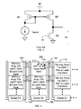
- FIGS. 1-3 depict portions of a conventional spin transfer torque magnetic random access memory (STT-RAM).
- FIG. 1 depicts a small portion of the STT-RAM 1 including a storage cell 10.
- FIG. 2 depicts the bit line sensing scheme, while FIG. 3 depicts a common source amplifier 50 used in connection with the memory 1.
- the conventional STT-RAM 1 utilizes spin transfer as a mechanism for switching the state of the magnetic storage cell.
- the conventional STT-RAM 1 includes a conventional magnetic storage cell 10 including a magnetic element 12 and a selection device 14.
- the selection device 14 is generally a transistor such as a NMOS transistor and includes a drain 11, a source 13, and a gate 15. Also depicted are a word line 16, a bit line 18, and source line 20.
- the word line 16 is oriented perpendicular to the bit line 18.
- the source line 20 is typically either parallel or perpendicular to the bit line 18, depending on specific architecture used for the conventional STT-RAM 1.
- the bit line 18 is connected to the magnetic element 12, while the source line 20 is connected to the source 13 of the selection device 14.
- the word line 16 is connected to the gate 15.
- the conventional STT-RAM 1 programs the magnetic memory cell 10 by driving a bi-directional current through the cell 10.
- the magnetic element 12 is configured to be changeable between high and low resistance states by a current flowing through the conventional magnetic element 12.
- the magnetic element 12 may be a magnetic tunneling junction (MTJ) or other magnetic structure that may be written using the spin transfer effect. Typically, this is achieved by ensuring that the magnetic element 12 has, for example, a sufficiently small cross-sectional area as well as other features desirable for switching using the spin transfer effect.
- the current density is sufficiently large, the current carriers driven through the magnetic element 12 may impart sufficient torque to change the state of the magnetic element 12.
- the write current is driven in one direction, the state may be changed from a low resistance state to a high resistance state.
- the write current passes through the magnetic element 12 in the opposite direction, the state may be changed from a high resistance state to a low resistance state.
- the word line 16 is high and turns on the selection device 14.
- the write current flows either from the bit line 18 to the source line 20, or vice versa, depending upon the state to be written to the magnetic memory cell 10.
- the column decoder 22 selects the desired bit lines 18.
- a row decoder (not shown in FIG. 2 also enables the appropriate word line(s) 16.
- the word line 16 is high, enabling the selection device 14. Consequently, a read current flows from the bit line 18 to the source line 20.
- reference currents are also driven through reference resistors Rref0 and Rref1.
- the output signals are provided to a sense amplifier, such as the conventional sense amplifier 50 shown in FIG. 3 .
- the conventional STT-RAM 1 may have better cell scalability and lower write current without suffering from the problem of write disturbance to the neighboring memory cells and smaller cell size for high memory density.
- STT-RAM 1 functions, one of ordinary skill in the art will readily recognize that the STT-RAM 1 is still desired to be improved. More specifically, it is desirable to provide an STT-RAM that is scalable and has sufficiently fast access times to continue development as a next-generation nonvolatile memory.
- the object of the invention is attained by a magnetic memory according to claim 1 and by the method for fabricating a magnetic memory according to claim 16. Further developments of the invention are specified in the dependent claims.
- the present invention provides a magnetic memory employing a hierarchical architecture, which may result in faster access times and increased write and/or read margins.
- the present invention relates to magnetic memories.
- the following description is presented to enable one of ordinary skill in the art to make and use the invention and is provided in the context of a patent application and its requirements.
- Various modifications to the preferred embodiments and the generic principles and features described herein will be readily apparent to those skilled in the art.
- the exemplary embodiments are mainly described in terms of particular methods and systems provided in particular implementations. However, the methods and systems will operate effectively in other implementations. Phrases such as "exemplary embodiment”, “one embodiment” and “another embodiment” may refer to the same or different embodiments.
- the embodiments will be described with respect to systems and/or devices having certain components.
- the systems and/or devices may include more or less components than those shown, and variations in the arrangement and type of the components may be made without departing from the scope of the invention.
- the exemplary embodiments will also be described in the context of particular methods having certain steps. However, the method and system operate effectively for other methods having different and/or additional steps and steps in different orders that are not inconsistent with the exemplary embodiments.
- the present invention is not intended to be limited to the embodiments shown, but is to be accorded the widest scope consistent with the principles and features described herein. Further, for clarity, the drawings are not to scale
- a method and system for providing a magnetic memory include providing memory array tiles (MATs), intermediate circuitry, global bit lines, global word lines, and global circuitry.
- Each MAT includes magnetic storage cells, bit lines, and word lines.
- Each of the magnetic storage cells includes at least one magnetic element and at least one selection device.
- the magnetic element(s) are programmable using write current(s) driven through the magnetic element(s).
- the bit lines and the word lines correspond to the magnetic storage cells.
- the intermediate circuitry controls read and write operations within the MATs.
- Each global bit line corresponds to a first portion of the plurality of MATs.
- Each global word line corresponds to a second portion of the MATs.
- the global circuitry selects and drives part of the global bit lines and part of the global word lines for the read and write operations.
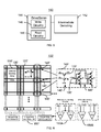
- FIG. 4 is a diagram of an exemplary embodiment of a portion of a magnetic memory 100 employing the spin transfer effect.
- the magnetic memory 100 is preferably a STT-RAM 100 and is organized in a hierarchical manner.
- the memory 100 includes memory array tiles (MATs) 110, global circuitry bit lines 120, global word lines 130, intermediate circuitry 140, and global circuitry 150. Although particular numbers of global bit lines 120, global word lines 130, intermediate circuitry 140, and global circuitry 150 are shown, As can be seen in FIG. 4 , the combination of MAT 110, global bit lines 120, global word lines 130, intermediate circuitry 140, and global circuitry 150 may be repeated to scale the magnetic memory 100 up to provide storage of a greater amount of data.
- the intermediate circuitry 140 controls writing operation(s) in the MAT 110 to its left and/or right.
- MATs 110 are shown. However, the memory 100 may include another number of MATs 110.
- the memory 100 array may be segregated into sub-arrays.
- a sub-array includes eight MATs 110, and nine word lines 112 are sandwiched by local decoding circuitry, such as column select circuits (not explicitly shown), which may be part of the intermediate circuitry 140.
- the even bit line/source line pairs 114 are connected to column select circuitry at the top intermediate circuitry 140, while the odd bit line/source line pairs 114 pairs are connected to the bottom column select circuitry at the bottom intermediate circuitry 140.
- the memory 100 operates synchronously with an external memory clock.
- Input control signals may be used to issue read and write commands together with address bits.
- eight bits of data may be read or written at the same time. However, other embodiment may read and/or write another number of bits of data.
- input signals are registered on the positive edge of clock.
- the positive clock cycle is used as memory active cycle and the negative cycle is used as memory pre-charge cycle.
- the MAT 110 is where data is actually stored. For clarity, only one MAT 110 is labeled with numeral "110".
- Each MAT includes multiple storage cells (not explicitly shown) that may be arranged in an array. Further, the array may be divided in one or more banks, which may be the same or different.
- Each storage cell may include one or more magnetic memory elements and one or more selection devices.
- a memory cell may include one magnetic tunneling junction and one selection transistor.
- a storage cell may include two magnetic tunneling junctions and two selection transistors. In other embodiments different numbers of magnetic elements and/or selection devices may be used.
- the magnetic element is programmable using at write current(s) driven through the magnetic element.
- a two transistor-two magnetic element storage cell is formed by combining two one transistor-one magnetic element storage cell.
- one of the two magnetic elements may be assigned the true bit and the other magnetic storage cell assigned the complement bit. Opposite states are written to the true and complement magnetic elements.
- Such a storage scheme allows for a differential sensing scheme to be used.
- An embodiment that uses a one transistor-one magnetic element may use a reference bit-line sensing scheme.
- the MAT 110 also includes bit lines and word lines.
- the bit lines and source lines run vertically and are shown by arrows 114, while word lines run horizontally, as shown by arrows 112.
- the bit lines 114 and the word lines 112 correspond to the magnetic storage cells.
- the magnetic storage cells are located cross points of the bit lines 114 and word lines 112.
- bit-lines 114 and source-lines 114 may be drawn at half-pitch similar to DRAM.
- Intermediate circuitry 140 controls read operations and write operations within the corresponding MATs 110.
- the intermediate circuitry 140 may include local decoding circuitry 142 and drive-sense circuitry 144.
- Decoding circuitry 142 may allow for selection of specific MAT(s) 110 as well as individual word lines 112 and bit lines 114 (and thus selected storage cells) within the MAT(s) 110.
- Write circuitry 146 may be used to drive write currents and otherwise control write operations within a MAT 110.
- read circuitry 148 may drive a read current, receive an output sense current from the MAT 110 being read, and/or otherwise control read operations in the corresponding MAT(s) 110.
- the global bit lines 120 and global word lines 130 may be used to select between MATs 110.
- different MATs 110 may be read or written to based on enabling and disabling of the global bit lines 120 and global word lines 130.
- the global circuitry 150 is also used for selecting and driving a portion of the global bit lines 120 and a portion of the global word lines 130 for the read operations and the write operations. In other words, the global circuitry may selectively enable/disable portions of the lines 120 and 130 as well as receiving signal(s) from the lines 120.
- the memory 100 is organized in a modular, hierarchical architecture. As a result, larger memories may be built by adding one or more of the modules 110, 120, 130, 140, and 150.
- the memory 100 is thus scalable to larger, more dense memories.
- the memory 100 might be scalable to gigabit (Gb) densities or beyond.
- Gb gigabit
- the global bit lines 120 and global word lines 130 may have a lower resistance than the bit lines 114 and word lines 112 within each MAT 110. In some embodiments, this may be achieved by forming the global lines 120 and 130 in the metal 3 layer. Thus, the parasitic resistance may be reduced and/or limited to the MATs 110. Array efficiency may thus be increased with little performance impact.
- Sense amplifiers may be located in the global circuitry 150 and thus de-coupled from the local bit lines 114. Multiple MATs 110 may also share a set of global sense amplifiers and global writer drivers in the global circuitry 150. In some embodiments, the array size may thus be reduced, for example by 40% over a memory having the same size but using localized sense amplifiers. Use of the intermediate circuitry 140 for sensing signals, driving currents, and decoding within the MATs may reduce read and/or write penalties. Consequently, the memory 100 may be usable in higher density memories, such as high density STT-RAM. Thus, the benefits of STT-RAM, such as lower power consumption, lower cost, and non-volatility may be scaled to higher density memories.
- FIG. 6 is a diagram of another exemplary embodiment of a portion of a magnetic 100' memory employing the spin transfer effect.
- the memory 100' includes MATs 110', global bit lines 120', global word lines 130', intermediate circuitry 140', and global circuitry 150'. Also shown are specific embodiments of the intermediate circuitry 140' and global circuitry 150'.
- the intermediate circuitry 140' includes read circuitry 148' and write circuitry 146'.
- the global circuitry 150' includes either circuitry 150A configured to sense read signals with respect to a reference signal and circuitry 150B configured to use differential sensing.
- the memory 100' includes intermediate circuitry 140'.
- the intermediate drive/sense circuitry 140' may drive current, receive signals from, and otherwise control read operations and write operations in the corresponding MATs 110', In the embodiment shown, the intermediate circuitry 140' controls such operations for the MAT(s) 110' to the right and/or left of the intermediate circuitry 140'.
- the intermediate circuitry 140' thus includes read circuitry 148' and write circuitry 146'.
- the read circuitry 148' controls read operations in the corresponding MAT(s) 110'.
- the read driver 140' is essentially a pass gate.
- the read circuitry 148' may include other components.
- the read circuitry 148' might include a preamplifier or other circuitry. Such a preamplifier may include a current mirror (not shown in FIG. 6 ).
- the write driver 146' is used to drive write current for write operations the corresponding MAT(s) 110.
- the write driver 146' is tri-stated during read operations.
- the global write line (GBWL) 130' is activated with valid data and the selected sub-array write drivers 146' are enabled to boost the write data signals on the source and bit lines 114'.
- the embodiment shown in FIG. 6 has a negative bit line/source line 114' boost option for increasing the write margin if necessary.
- a pull down transistor source node of the write driver 146' is connected to a bus which is normally grounded.
- the word line 112 is boosted to 3.2v to provide a write current sufficient to write a "1" (change the magnetization of the free layer of a MTJ from antiparallel to the pinned layer magnetization to parallel to the pinned layer magnetization). In one embodiment, this write current is 128 ⁇ A. In one embodiment, to write a "0" (change the magnetization of the free layer of a MTJ from parallel to the pinned layer magnetization to antiparallel to the pinned layer magnetization), a write current of approximately 152 ⁇ A may be used. In one such embodiment, the MTJ used as the magnetic element is designed to switch at ⁇ 80 ⁇ A, which may provide a write margin greater than 60%. However, other write currents, other magnetic elements switching at different currents, and other schemes might be used. Because the write drivers 146' are repeated locally in the array gap between the MATs 140, there may be little no impact to write margin at higher densities using this architecture.
- the memory 100' also includes global circuitry 150'.
- Global circuitry 150A and 150B that are configured for reference and differential sensing, respectively.
- the global circuitry 150A may be used in an embodiment in which each storage cell includes a single transistor and a single magnetic element such as an MTJ.
- the global circuitry 150B may be used for a MAT 110 in which each cell includes two transistors and two magnetic elements and in which a bit and its complement are stored.
- the global circuitry 150A and 150B each include sense amplifiers (SA) that are used to provide an output corresponding to the state(s) of the storage cells in the MATs 110.
- SA sense amplifiers
- the memory 100' may share the benefits of the memory 100.
- the memory 100' is organized in a modular, hierarchical architecture.
- the memory 100' is thus scalable to larger, more dense memories.
- the memory 100' might be scalable to Gb densities or beyond.
- the global bit lines 120' and global word lines 130' may have a lower resistance than the lines 114' and 112' within each MAT 110'.
- the parasitic resistance may be reduced and/or limited to the MATs 110.
- Array efficiency may thus be increased with little performance impact. Short write times and small read access times might also be achieved.
- Sense amplifiers may be located in the global circuitry 150', be de-coupled from the local bit lines, and be shared by multiple MATs 110'. The array size may thus be reduced.
- Use of the intermediate circuitry 140' may reduce read and/or write penalties.
- the benefits of STT-RAM such as lower power consumption, lower cost, and non-volatility may be scaled to higher density memories.
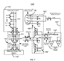
- FIG. 7 is a diagram of another exemplary embodiment of a portion of a magnetic memory 100" employing the spin transfer effect.
- the memory 100 includes MATs 110", global bit lines 120", global word lines 130", intermediate circuitry 140", and global circuitry 150".
- the intermediate circuitry 140 includes write circuitry 146" and read circuitry 148".
- the global circuitry 150 is shown as including circuitry 150A' configured to sense read signals with respect to a reference signal.
- the memory 100 may be segregated into sub-arrays.
- a sub-array includes eight MATs 110" with nine word lines 112 are sandwiched by local decoding circuitry, such as local column select circuits 142', which may be part of the intermediate circuitry 140".
- the even bit line/source line pairs 114" are connected to column select circuitry at the top intermediate circuitry 140", while the odd bit line/source line pairs 114" pairs are connected to the bottom column select circuitry at the bottom intermediate circuitry 140".
- the column select signal CS of the local column select circuitry 142' may also be a global signal that may run across multiple MAT(s) 110".
- the global circuitry 150" may include a column decoder (not shown) providing the column select signal CS.
- isolation transistors driven by lines 141 and 143.
- the MAT 110 being accessed may be selected and the MAT(s) 110 not being accessed may be isolated.
- five address bits decode one of 32 global column-select lines, while three bits decode one of eight sections.
- Each MAT 110 might include 16Kbit of STT-RAM, four reference bit line/source lines 114", sixteen redundant word lines 112", eight redundant bit line/source lines 114", and four redundant reference bit line/source lines 114".
- most of the parasitic resistances in the read path are in the bit lines and source lines 114 (not explicitly labeled in FIG. 7 ), which may be located within metal 1 and metal 0, respectively.
- the architecture depicted in FIG. 7 may thus scalable to higher densities because multiple MATs 110 may be added with minor impact to sense amplifier margin.
- the magnetic memory 100" operates in an analogous manner to the memories 100 and 100'.
- the memory 100" may share the benefits of the memory 100 and 100'.
- the memory 100' is organized in a modular, hierarchical architecture.
- the memory 100" is thus scalable to larger, more dense memories.
- the global bit lines 120" and global word lines 130" may have a lower resistance.
- the parasitic resistance may be reduced and/or limited to the MATs 110".
- Array efficiency may thus be increased with little performance impact. Short write times and small read access times might also be achieved.
- Sense amplifiers may be located in the global circuitry 150", be de-coupled from the local bit lines, and be shared by multiple MATs 110". The array size may thus be reduced.
- Use of the intermediate circuitry 140" may reduce read and/or write penalties.
- the benefits of STT-RAM such as lower power consumption, lower cost, and non-volatility may be scaled to higher density memories.
- FIG. 8 is a diagram of another exemplary embodiment of a portion of a MAT 110"'.
- a storage cell 115 including magnetic element 116 is shown.
- the storage cell 115 shown includes one magnetic element 116 and one selection device.
- the magnetic element 116 may be a magnetic tunneling junction or other analogous structure that is switchable via spin transfer.
- the selection device may be a selection transistor.
- bit line 114A, source line 114B are also shown.
- the memory cell dimension may be 216nm x 188nm, or 14F 2 .
- two polysilicon word-lines 112'" in parallel make up the gate of the selection transistor
- the source line 114B may be formed in the metal 0 layer, while the bit line 114A is formed in the metal 1 line. Also in the embodiment shown, the bit line 114A and source line 114B are perpendicular to the word lines 112"'.
- the word lines 112'" are driven by word line drivers that are part of decoding circuitry 142 (not shown in FIG. 8 ) and decoded using a hierarchical row decoding scheme. In one embodiment, three address bits decode one of eight word lines 112"'. Thus, eight word lines 112"' are selected at once by a global word-line driver (not shown in FIG.
- a portion of the remaining address bits select one of the sixteen global word lines 130 within a sub-array section. Remaining bits may be decoded to select one of four sub-array sections in a block.
- the global word line 140 may reside in the metal 2 that runs across the entire length of the sub-array.
- FIG. 9 is a diagram of another exemplary embodiment of a portion of a magnetic memory 100"' employing the spin transfer effect including a preamplifier. More specifically, the portion of the magnetic memory 100"' includes read circuitry 148"' that is part of intermediate circuitry such as the intermediate circuitry 140/140'. Also shown are other portions of the memory, including decoding circuitry, for example as shown in the column select transistors receiving column select signals CS0-CSn. As discussed above, the intermediate circuitry 140/140' may include passgate(s) and/or preamplifiers. The read circuitry 148"' includes a preamplifier 148"'. The preamplifier 148"' shown is configured to activate when the enable signal ENB is low.
- the preamplifier 148"' may be configured in another manner.
- the preamplifier is a current mirror preamplifier, using transistor pairs M1 and M2 to form the current mirror.
- M2 equals N*M1, where N is greater than one. Therefore, the current mirror preamplifier 148 outputs an amplified current that is N times the input read current.
- the preamplifier 148"' amplifies the read signal from the magnetic elements 116' by a factor of N. Thus, a lower read current may be used within the MATs 110/110'.
- the transistors M1 may have a width designed to provide a small read current that is well under the switching current of the magnetic element(s) of the storage cell. Thus, a read operation may be performed without disturbing the state of the storage cells in the MAT(s) 110/110'/110". In addition, power dissipation by read current carried by higher resistance bit and source lines 114 may be reduced. Using M2 transistors having widths designed to provide sufficient amplification allows for a higher output current. Thus, more robust sensing is achieved. Note that sense amp current path is decoupled from the current path of the magnetic element. The preamplifier 148"' thus amplifies the read current from the MAT(s) 110/110' and may drive the current to global circuitry 150/150'. More specifically, in the embodiment shown, the amplified current may be provided to sense amplifier 170 that may be part of the global circuitry 150/150'.
- the magnetic memory 100"' may share the benefits of the memories 100, 100', and 100".
- the preamplifier 148"' because of the use of the preamplifier 148"', there may be little or no read penalty. More specifically, as discussed above, a lower read current may be used within the MATs 110/110'/110", amplified by the preamplifier 148"', and the amplified current may be provided to the sense amplifier 170 for determination of the state of the storage cell being read. Consequently, performance may be improved.
- FIG. 10 is a diagram of an exemplary embodiment of the stages of a sense amplifier 170' usable in a memory, such as the memory 100/100'/100"/100"' employing the spin transfer effect.
- the sense amplifier 170' may be used in global circuitry 150/150'/150".
- the sense amplifier 170' may include stages 172 and 174.
- the first stage 172 may be a current stage.
- the first stage 172 may be repeated as a first voltage stage. In such an embodiment, therefore, the first stage 172 may be used for two of three stages of the sense amplifier 170'.
- the second stage 174 may be a second voltage stage.
- the sense amplifier 170' includes two stages. However, in another embodiment, the sense amplifier 170' may include another number of stages. Further, in another embodiment, the memory 100/100'/100"/100"' may use another sense amplifier (not shown).
- the bit line 120 that carry data and, in some embodiments, a reference act as the current source loads to a pair of common source amplifiers.
- the signal V CM is a bias voltage that controls the current source as well as the output voltage. However, control of the current source and the output voltage may be separated for independent control.
- I BL is the current provided for read operations.
- the sense amplifier 170' may provide the read current and receive a read current as a load. However, in another embodiment, the read current may be decoupled from the sense amplifier 170'.
- the circuit 172 used in the first current and first voltage stages are powered using which is less than the power supply voltage.
- the combination of V CM and the voltage powering the circuit 172 results in a controlled read voltage across the magnetic element 116.
- the sense amplifier 170' may be used in the reference scheme (e.g. one transistor-one magnetic element per storage cell) as well as in a differential sensing scheme (two transistors and two magnetic elements storing complementary data per storage cell). Note that the sensing margin may be doubled with the differential sensing scheme.
- FIG. 11 is a diagram of another exemplary embodiment of a write driver 146"' usable in a memory employing the spin transfer effect.
- the write driver is analogous to the write driver 146" depicted in FIG. 7 .
- global circuitry 150/150' drives GWRL high.
- the bit line 114A is high, while the source line 114B is driven low.
- the write driver 146'" may also drive write current(s) in the MAT(s) 110/110'/110"/110”'.
- use of the write driver 146"' in the intermediate circuitry 140/140'/140" of the memory 100, 100', 100", 100"' may allow for at least some of the benefits of the intermediate circuitry 140/140'/140" to be achieved.
- FIG. 12 is a diagram of an exemplary embodiment of a method 200 for providing a magnetic memory employing the spin transfer effect.
- the method 200 is described in context of the memory 100 in FIG. 4 . However, in alternate embodiments, other configurations may be used.
- the method 200 is described in the context of particular steps. However, steps may be combined or omitted.
- step 202 includes providing one or more arrays, each of which includes multiple magnetic storage cells. Further, bit and source lines 114, plurality of word lines 112, within the MATs are provided. Intermediate circuitry 140 for controlling read operations and write operations within the plurality of MATs are provided, via step 204. Step 204 may include providing decoding circuitry 142, and read/write circuitry 144 that may include write driver(s) 146 and read drivers 148. Global bit lines 120 are provided, via step 206. Similarly, global word lines 130 are provided, via step 208. Global circuitry 150 is also provided, via step 210. Fabrication of the memory 100 may then be completed.
- the memory 100, 100', 100", and/or 100"' may be provided. Consequently, the benefits of the hierarchical architecture of the memories 100, 100' might be achieved.
Landscapes
- Engineering & Computer Science (AREA)
- Computer Hardware Design (AREA)
- Mram Or Spin Memory Techniques (AREA)
- Hall/Mr Elements (AREA)
- Semiconductor Memories (AREA)
Claims (16)
- Magnetspeicher, aufweisend:eine Mehrzahl an Speicherfeldkacheln (110; 110', 110", 110"'), wobei jede von der Mehrzahl an Speicherfeldkacheln (110, 110', 110", 110"') eine Mehrzahl an Magnetspeicherzellen, eine Mehrzahl an Bitleitungen (114) und eine Mehrzahl an Wortleitungen (112) aufweist, wobei jede von der Mehrzahl an Magnetspeicherzellen zumindest ein Magnetelement und zumindest eine Auswahleinrichtung beinhaltet, wobei das zumindest eine Magnetelement unter Verwendung zumindest eines Schreibstroms, der durch das zumindest eine Magnetelement geleitet wird, programmierbar ist, wobei die Mehrzahl an Bitleitungen (114) und die Mehrzahl an Wortleitungen (112) der Mehrzahl an Magnetspeicherzellen entsprechen;eine Zwischenschaltung (140; 140', 140") zum Steuern von Lesevorgängen und Schreibvorgängen innerhalb der Mehrzahl an Speicherfeldkacheln (110; 110', 110", 110"');eine Mehrzahl an globalen Bitleitungen (120; 120', 120"), wobei jede von den globalen Bitleitungen (120; 120', 120") einem ersten Abschnitt der Mehrzahl an Speicherfeldkacheln (110; 110', 110", 110"') entspricht;eine Mehrzahl an globalen Wortleitungen (130; 130', 130"), wobei jede von den globalen Wortleitungen (130; 130', 130") einem zweiten Abschnitt der Mehrzahl an Speicherfeldkacheln (110; 110'; 110"; 110"') entspricht; undeine globale Schaltung (150; 150', 150") zum Auswählen und Treiben eines Abschnitts von der Mehrzahl an globalen Bitleitungen (120; 120', 120") und eines Abschnitts von der Mehrzahl an globalen Wortleitungen (130; 130', 130") für die Lesevorgänge und die Schreibvorgänge,wobei der Magnetspeicher dadurch gekennzeichnet ist, dassjede der globalen Bitleitungen (120; 120', 120") zwischen die globale Schaltung (150; 150', 150") und die Zwischenschaltung (140; 140', 140") geschaltet ist;jede der globalen Wortleitungen (130; 130', 130") zwischen die globale Schaltung (150; 150', 150") und die Zwischenschaltung (140; 140', 140") geschaltet ist; unddie Zwischenschaltung (140; 140', 140") ferner beinhaltet:eine Mehrzahl an Zwischen-Treiber/Erfassungs-Schaltungen (146, 148; 146', 148'; 146", 148"; 146"', 148"') zum Treiben von zumindest einem von den Lesevorgängen und den Schreibvorgängen in der Mehrzahl an Speicherfeldkacheln (110; 110'; 110"; 110"'), wobei jede von der Mehrzahl an Zwischentreibern einem dritten Abschnitt von der Mehrzahl an Speicherfeldkacheln (110; 110'; 110"; 110"') entspricht; undeine lokale Entschlüsselungsschaltung (142, 142') zum Auswählen von zumindest einer ausgewählten Speicherfeldkachel aus der Mehrzahl an Speicherfeldkacheln (110; 110'; 110"; 110"') und zumindest einer der Speicherzellen in der zumindest einen ausgewählten Speicherfeldkachel.
- Magnetspeicher nach Anspruch 1, wobei die Zwischenschaltung (140; 140', 140") ferner beinhaltet:eine Mehrzahl an Zwischenlesetreibern (148; 148'; 148"; 148"'), wobei jeder von der Mehrzahl an Zwischenlesetreibern (148; 148'; 148"; 148"') dazu dient, Lesevorgänge in einem dritten Abschnitt von der Mehrzahl an Speicherfeldkacheln (110; 110'; 110"; 110"') zu steuern; undeine Mehrzahl an Zwischenschreibtreibern (146; 146'; 146"; 146"'), wobei jede von der Mehrzahl an Schreibtreibern (146; 146'; 146"; 146"') dazu dient, Schreibvorgänge in einem vierten Abschnitt von der Mehrzahl an Speicherfeldkacheln (110; 110', 110"; 110"') anzusteuern.
- Magnetspeicher nach Anspruch 2, wobei jeder der Zwischenlesetreiber (148"') ferner beinhaltet:zumindest einen Vorverstärker zum Verstärken eines Lesesignals von dem Abschnitt von der Mehrzahl an Speicherfeldkacheln (110"'), um ein verstärktes Lesesignal bereitzustellen.
- Magnetspeicher nach Anspruch 3, wobei der zumindest eine Vorverstärker ferner beinhaltet:zumindest einen Stromspiegel-Vorverstärker.
- Magnetspeicher nach Anspruch 3, wobei die globale Schaltung (150; 150'; 150") ferner beinhaltet:zumindest einen Leseverstärker (170; 170') zum Empfangen eines verstärkten Lesesignals von dem Vorverstärker und zum Bereitstellen eines Ausgangs, der zumindest einem Zustand von zumindest einer von der Mehrzahl an Speicherzellen in dem Abschnitt von der Mehrzahl an Speicherfeldkacheln (110; 110'; 110"; 110"') entspricht.
- Magnetspeicher nach Anspruch 5, wobei der zumindest eine Leseverstärker (170) ferner beinhaltet:eine erste Stromstufe (172); undeine Spannungsstufe, die mit der ersten Stromstufe (174) gekoppelt ist.
- Magnetspeicher nach Anspruch 5, wobei der zumindest eine Leseverstärker (170) ferner beinhaltet:eine erste Stromstufe (172);eine erste Spannungsstufe (174), die mit der ersten Stromstufe (172) gekoppelt ist; undeine zweite Spannungsstufe, die mit der ersten Spannungsstufe (174) gekoppelt ist.
- Magnetspeicher nach Anspruch 2, wobei jeder von der Mehrzahl an Lesetreibern (148; 148'; 148"; 148"') ferner beinhaltet:ein Durchgangsgatter, das dem dritten Abschnitt der Speicherfeldkacheln (110; 110'; 110"; 110"') entspricht.
- Magnetspeicher nach Anspruch 1, wobei die Mehrzahl an globalen Wortleitungen (130; 130'; 130") einen ersten Widerstand aufweist, die Mehrzahl an globalen Bitleitungen (120; 120'; 120") einen zweiten Widerstand aufweist, die Mehrzahl an Wortleitungen (112) einen dritten Widerstand aufweist, und die Mehrzahl an Bitleitungen (114) einen vierten Widerstand aufweist, wobei der erste Widerstand geringer ist als der dritte Widerstand und der vierte Widerstand, und der zweite Widerstand geringer ist als der dritte Widerstand und der vierte Widerstand.
- Magnetspeicher nach Anspruch 1, wobei die globale Schaltung (150; 150'; 150") ferner beinhaltet:zumindest einen Leseverstärker (170; 170') zum Empfangen eines Lesesignals von dem Abschnitt von der Mehrzahl an Speicherfeldkacheln, der so konfiguriert ist, dass er das Lesesignal in einem Differentialerfassungsverfahren verarbeitet.
- Magnetspeicher nach Anspruch 1, wobei die globale Schaltung (150; 150'; 150") ferner beinhaltet:zumindest einen Leseverstärker (170; 170') zum Empfangen eines Lesesignals von dem Abschnitt von der Mehrzahl an Speicherfeldkacheln (110; 110'; 110"; 110"'), der so konfiguriert ist, dass er das Lesesignal auf Basis eines Referenzsignals verarbeitet.
- Magnetspeicher nach Anspruch 1, wobei die Mehrzahl an Speicherfeldkacheln (110; 110'; 110"; 110"') ferner beinhaltet:eine erste Bank; undeine zweite Bank, die sich von der ersten Bank unterscheidet.
- Magnetspeicher nach Anspruch 1, wobei jede Zelle von zumindest einem Abschnitt von der Mehrzahl an Speicherzellen einen einzelnen Transistor und ein einzelnes magnetisches Element beinhaltet.
- Magnetspeicher nach Anspruch 1, wobei jede Zelle von zumindest einem Abschnitt von der Mehrzahl an Speicherzellen zwei Transistoren und zwei magnetische Elemente beinhaltet.
- Magnetspeicher nach Anspruch 14, wobei die zwei Transistoren und die zwei magnetischen Elemente dazu konfiguriert sind, mit einem Differentialerfassungsverfahren gelesen werden.
- Verfahren zum Herstellen eines Magnetspeichers, aufweisend:Bereitstellen einer Mehrzahl an Speicherfeldkacheln (110; 110'; 110"; 110"'), wobei jede von der Mehrzahl an Speicherfeldkacheln (110; 110'; 110"; 110"') eine Mehrzahl an Magnetspeicherzellen, eine Mehrzahl an Bitleitungen (114) und eine Mehrzahl an Wortleitungen (112) aufweist, wobei jede von der Mehrzahl an Magnetspeicherzellen zumindest ein magnetisches Element und zumindest eine Auswahleinrichtung beinhaltet, wobei das zumindest eine magnetische Element unter Verwendung von zumindest einem Schreibstrom, der durch das zumindest eine magnetische Element geleitet wird, programmierbar ist, und die Mehrzahl an Bitleitungen (114) und die Mehrzahl an Wortleitungen (112) der Mehrzahl an Magnetspeicherzellen entsprechen;Bereitstellen einer Zwischenschaltung (140; 140', 140") zum Steuern von Lesevorgängen und Schreibvorgängen innerhalb der Mehrzahl an Speicherfeldkacheln (110; 110', 110", 110"');Bereitstellen einer Mehrzahl an globalen Bitleitungen (120; 120', 120"), wobei jede von den globalen Bitleitungen (110; 110', 110") einem ersten Abschnitt der Mehrzahl an Speicherfeldkacheln (110; 110', 110", 110"') entspricht;Bereitstellen einer Mehrzahl an globalen Wortleitungen (130; 130', 130"), wobei jede von den globalen Wortleitungen (120; 120', 120") einem zweiten Abschnitt der Mehrzahl an Speicherfeldkacheln (110; 110'; 110"; 110"') entspricht; undBereitstellen einer globalen Schaltung (150; 150', 150") zum Auswählen und Treiben eines Abschnitts von der Mehrzahl an globalen Bitleitungen (120; 120', 120") und eines Abschnitts von der Mehrzahl an globalen Wortleitungen (130; 130', 130") für die Lesevorgänge und die Schreibvorgänge, wobei das Verfahren dadurch gekennzeichnet ist, dassjede der globalen Bitleitungen (120; 120', 120") zwischen die globale Schaltung (150; 150', 150") und die Zwischenschaltung (140; 140', 140") geschaltet ist;jede der globalen Wortleitungen (130; 130', 130") zwischen die globale Schaltung (150; 150', 150") und die Zwischenschaltung (140; 140', 140") geschaltet ist; unddie Zwischenschaltung (140; 140', 140") ferner beinhaltet:eine Mehrzahl an Zwischen-Treiber/Erfassungs-Schaltungen (146, 148; 146', 148'; 146", 148"; 146"', 148"') zum Treiben von zumindest einem von den Lesevorgängen und den Schreibvorgängen in der Mehrzahl an Speicherfeldkacheln (110; 110'; 110"; 110"'), wobei jede von der Mehrzahl an Zwischen-Treiber/Erfassungs-Schaltungen (146, 148; 146', 148'; 146", 148"; 146"', 148"') einem dritten Abschnitt von der Mehrzahl an Speicherfeldkacheln (110; 110'; 110"; 110"') entspricht; undeine lokale Decodierschaltung (142, 142') zum Auswählen von zumindest einer ausgewählten Speicherfeldkachel aus der Mehrzahl an Speicherfeldkacheln (110; 110'; 110"; 110"') und zumindest einer der Speicherzellen in der zumindest einen ausgewählten Speicherfeldkachel.
Applications Claiming Priority (3)
| Application Number | Priority Date | Filing Date | Title |
|---|---|---|---|
| US24185609P | 2009-09-11 | 2009-09-11 | |
| US12/565,273 US8385106B2 (en) | 2009-09-11 | 2009-09-23 | Method and system for providing a hierarchical data path for spin transfer torque random access memory |
| PCT/US2010/047941 WO2011031655A1 (en) | 2009-09-11 | 2010-09-07 | Method and system for providing a hierarchical data path for spin transfer torque random access memory |
Publications (3)
| Publication Number | Publication Date |
|---|---|
| EP2476121A1 EP2476121A1 (de) | 2012-07-18 |
| EP2476121A4 EP2476121A4 (de) | 2013-04-17 |
| EP2476121B1 true EP2476121B1 (de) | 2014-05-21 |
Family
ID=43730408
Family Applications (1)
| Application Number | Title | Priority Date | Filing Date |
|---|---|---|---|
| EP10815956.7A Active EP2476121B1 (de) | 2009-09-11 | 2010-09-07 | Verfahren und system zur bereitstellung eines hierarchischen datenpfades für einen stt-direktzugriffsspeicher |
Country Status (6)
| Country | Link |
|---|---|
| US (1) | US8385106B2 (de) |
| EP (1) | EP2476121B1 (de) |
| JP (1) | JP6066288B2 (de) |
| KR (1) | KR101777802B1 (de) |
| CN (1) | CN102483956B (de) |
| WO (1) | WO2011031655A1 (de) |
Families Citing this family (32)
| Publication number | Priority date | Publication date | Assignee | Title |
|---|---|---|---|---|
| US8982649B2 (en) * | 2011-08-12 | 2015-03-17 | Gsi Technology, Inc. | Systems and methods involving multi-bank, dual- or multi-pipe SRAMs |
| US8711646B2 (en) | 2012-05-08 | 2014-04-29 | Samsung Electronics Co., Ltd. | Architecture, system and method for testing resistive type memory |
| US9076541B2 (en) * | 2013-03-14 | 2015-07-07 | Samsung Electronics Co., Ltd. | Architecture for magnetic memories including magnetic tunneling junctions using spin-orbit interaction based switching |
| US9286959B2 (en) | 2013-11-18 | 2016-03-15 | International Business Machines Corporation | Low latency memory access control for non-volatile memories |
| KR101582731B1 (ko) * | 2014-01-07 | 2016-01-08 | 한양대학교 산학협력단 | 저항성 메모리의 감지증폭회로 |
| JP2015185179A (ja) * | 2014-03-20 | 2015-10-22 | 株式会社東芝 | 抵抗変化メモリ |
| KR102151183B1 (ko) | 2014-06-30 | 2020-09-02 | 삼성전자주식회사 | 저항성 메모리 장치 및 저항성 메모리 장치의 동작방법 |
| US10854284B1 (en) | 2016-12-06 | 2020-12-01 | Gsi Technology, Inc. | Computational memory cell and processing array device with ratioless write port |
| US10777262B1 (en) | 2016-12-06 | 2020-09-15 | Gsi Technology, Inc. | Read data processing circuits and methods associated memory cells |
| US10847212B1 (en) | 2016-12-06 | 2020-11-24 | Gsi Technology, Inc. | Read and write data processing circuits and methods associated with computational memory cells using two read multiplexers |
| US10249362B2 (en) | 2016-12-06 | 2019-04-02 | Gsi Technology, Inc. | Computational memory cell and processing array device using the memory cells for XOR and XNOR computations |
| US10860320B1 (en) | 2016-12-06 | 2020-12-08 | Gsi Technology, Inc. | Orthogonal data transposition system and method during data transfers to/from a processing array |
| US10847213B1 (en) | 2016-12-06 | 2020-11-24 | Gsi Technology, Inc. | Write data processing circuits and methods associated with computational memory cells |
| US10725777B2 (en) | 2016-12-06 | 2020-07-28 | Gsi Technology, Inc. | Computational memory cell and processing array device using memory cells |
| US10943648B1 (en) | 2016-12-06 | 2021-03-09 | Gsi Technology, Inc. | Ultra low VDD memory cell with ratioless write port |
| US11227653B1 (en) | 2016-12-06 | 2022-01-18 | Gsi Technology, Inc. | Storage array circuits and methods for computational memory cells |
| US10891076B1 (en) | 2016-12-06 | 2021-01-12 | Gsi Technology, Inc. | Results processing circuits and methods associated with computational memory cells |
| US10770133B1 (en) | 2016-12-06 | 2020-09-08 | Gsi Technology, Inc. | Read and write data processing circuits and methods associated with computational memory cells that provides write inhibits and read bit line pre-charge inhibits |
| WO2018232766A1 (zh) | 2017-06-23 | 2018-12-27 | 华为技术有限公司 | 存储器和写数据的方法 |
| JP2019053794A (ja) * | 2017-09-13 | 2019-04-04 | 東芝メモリ株式会社 | 半導体記憶装置 |
| IT201800000555A1 (it) * | 2018-01-04 | 2019-07-04 | St Microelectronics Srl | Architettura di decodifica di riga per un dispositivo di memoria non volatile a cambiamento di fase e relativo metodo di decodifica di riga |
| CN110136760B (zh) * | 2018-02-09 | 2021-03-23 | 上海磁宇信息科技有限公司 | Mram芯片 |
| CN110136761A (zh) * | 2018-02-09 | 2019-08-16 | 上海磁宇信息科技有限公司 | 一种高带宽的磁性随机存储器 |
| US10877731B1 (en) | 2019-06-18 | 2020-12-29 | Gsi Technology, Inc. | Processing array device that performs one cycle full adder operation and bit line read/write logic features |
| US10930341B1 (en) | 2019-06-18 | 2021-02-23 | Gsi Technology, Inc. | Processing array device that performs one cycle full adder operation and bit line read/write logic features |
| US10958272B2 (en) | 2019-06-18 | 2021-03-23 | Gsi Technology, Inc. | Computational memory cell and processing array device using complementary exclusive or memory cells |
| KR102651232B1 (ko) | 2019-07-18 | 2024-03-25 | 삼성전자주식회사 | 자기접합 메모리 장치 및 자기접합 메모리 장치의 데이터 리드 방법 |
| KR102651229B1 (ko) | 2019-07-22 | 2024-03-25 | 삼성전자주식회사 | 자기접합 메모리 장치 및 자기접합 메모리 장치의 데이터 라이트 방법 |
| CN110739010B (zh) * | 2019-10-21 | 2021-05-11 | 中国科学院上海微系统与信息技术研究所 | 低温存储单元及存储器件 |
| US11264070B2 (en) | 2020-01-16 | 2022-03-01 | Taiwan Semiconductor Manufacturing Company Limited | Systems and methods for memory operation using local word lines |
| US11170843B2 (en) * | 2020-03-19 | 2021-11-09 | Arm Limited | Bitcell with multiple read bitlines |
| US12482520B2 (en) * | 2022-11-23 | 2025-11-25 | The Trustees Of Columbia University In The City Of New York | 6T-SRAM-based digital computing-in-memory circuits supporting flexible input dimension |
Family Cites Families (23)
| Publication number | Priority date | Publication date | Assignee | Title |
|---|---|---|---|---|
| JPH0729373A (ja) * | 1993-07-08 | 1995-01-31 | Mitsubishi Electric Corp | 半導体記憶装置 |
| US6611405B1 (en) * | 1999-09-16 | 2003-08-26 | Kabushiki Kaisha Toshiba | Magnetoresistive element and magnetic memory device |
| JP2002093158A (ja) * | 2000-09-08 | 2002-03-29 | Hitachi Ltd | 半導体装置およびメモリシステム |
| FR2817998B1 (fr) * | 2000-12-07 | 2003-01-10 | Commissariat Energie Atomique | Dispositif magnetique a polarisation de spin et a rotation d'aimantation, memoire et procede d'ecriture utilisant ce dispositif |
| FR2817999B1 (fr) * | 2000-12-07 | 2003-01-10 | Commissariat Energie Atomique | Dispositif magnetique a polarisation de spin et a empilement(s) tri-couche(s) et memoire utilisant ce dispositif |
| KR100374792B1 (ko) * | 2000-12-29 | 2003-03-04 | 삼성전자주식회사 | 수직 자기 기록 디스크 |
| US6744086B2 (en) | 2001-05-15 | 2004-06-01 | Nve Corporation | Current switched magnetoresistive memory cell |
| US6469560B1 (en) * | 2001-06-28 | 2002-10-22 | Faraday Technology Corp. | Electrostatic discharge protective circuit |
| FR2829868A1 (fr) * | 2001-09-20 | 2003-03-21 | Centre Nat Rech Scient | Memoire magnetique a ecriture par courant polarise en spin, mettant en oeuvre des alliages amorphes ferrimagnetiques et procede pour son ecriture |
| US6741496B2 (en) * | 2001-09-27 | 2004-05-25 | Intel Corporation | Electron spin mechanisms for inducing magnetic-polarization reversal |
| US6760243B2 (en) * | 2002-03-19 | 2004-07-06 | Broadcom Corporation | Distributed, highly configurable modular predecoding |
| TWI222763B (en) * | 2002-03-29 | 2004-10-21 | Toshiba Corp | Magnetic logic element and magnetic logic element array |
| JP2004213829A (ja) * | 2003-01-08 | 2004-07-29 | Renesas Technology Corp | 半導体記憶装置 |
| US7602000B2 (en) * | 2003-11-19 | 2009-10-13 | International Business Machines Corporation | Spin-current switched magnetic memory element suitable for circuit integration and method of fabricating the memory element |
| US7283333B2 (en) * | 2004-02-11 | 2007-10-16 | Hitachi Global Storage Technologies Netherlands B.V. | Self-pinned double tunnel junction head |
| US6995615B2 (en) * | 2004-05-20 | 2006-02-07 | Elantec Semiconductor, Inc | Current-mode preamplifiers |
| US7268586B1 (en) * | 2004-11-08 | 2007-09-11 | Tabula, Inc. | Method and apparatus for accessing stored data in a reconfigurable IC |
| JP4388008B2 (ja) * | 2004-11-30 | 2009-12-24 | 株式会社東芝 | 半導体記憶装置 |
| DE602005022398D1 (de) * | 2004-11-30 | 2010-09-02 | Toshiba Kk | Anordnung der Schreiblinien in einer MRAM-Vorrichtung |
| JP5035620B2 (ja) * | 2005-09-14 | 2012-09-26 | 日本電気株式会社 | 磁気ランダムアクセスメモリの波形整形回路 |
| JP4935183B2 (ja) * | 2006-05-18 | 2012-05-23 | 株式会社日立製作所 | 半導体装置 |
| US7782661B2 (en) * | 2007-04-24 | 2010-08-24 | Magic Technologies, Inc. | Boosted gate voltage programming for spin-torque MRAM array |
| US7764536B2 (en) * | 2007-08-07 | 2010-07-27 | Grandis, Inc. | Method and system for providing a sense amplifier and drive circuit for spin transfer torque magnetic random access memory |
-
2009
- 2009-09-23 US US12/565,273 patent/US8385106B2/en active Active
-
2010
- 2010-09-07 CN CN201080040444.8A patent/CN102483956B/zh active Active
- 2010-09-07 JP JP2012528848A patent/JP6066288B2/ja active Active
- 2010-09-07 KR KR1020127006295A patent/KR101777802B1/ko active Active
- 2010-09-07 WO PCT/US2010/047941 patent/WO2011031655A1/en not_active Ceased
- 2010-09-07 EP EP10815956.7A patent/EP2476121B1/de active Active
Also Published As
| Publication number | Publication date |
|---|---|
| US20110063898A1 (en) | 2011-03-17 |
| WO2011031655A1 (en) | 2011-03-17 |
| EP2476121A1 (de) | 2012-07-18 |
| EP2476121A4 (de) | 2013-04-17 |
| KR20120083323A (ko) | 2012-07-25 |
| CN102483956A (zh) | 2012-05-30 |
| CN102483956B (zh) | 2016-09-21 |
| JP6066288B2 (ja) | 2017-01-25 |
| KR101777802B1 (ko) | 2017-09-12 |
| US8385106B2 (en) | 2013-02-26 |
| JP2013504835A (ja) | 2013-02-07 |
Similar Documents
| Publication | Publication Date | Title |
|---|---|---|
| US8385106B2 (en) | Method and system for providing a hierarchical data path for spin transfer torque random access memory | |
| KR100505769B1 (ko) | 데이터 판독 참조용 더미셀을 구비한 박막 자성체 기억 장치 | |
| JP4726292B2 (ja) | 薄膜磁性体記憶装置 | |
| KR100654266B1 (ko) | 자기 터널 접합부를 갖는 박막 자성체 기억 장치 | |
| US7272034B1 (en) | Current driven switching of magnetic storage cells utilizing spin transfer and magnetic memories using such cells | |
| US7272035B1 (en) | Current driven switching of magnetic storage cells utilizing spin transfer and magnetic memories using such cells | |
| JP5091969B2 (ja) | 半導体記憶装置 | |
| US20030123281A1 (en) | Magnetic random access memory | |
| US20090040855A1 (en) | Method and system for providing a sense amplifier and drive circuit for spin transfer torque magnetic random access memory | |
| US6903965B2 (en) | Thin film magnetic memory device permitting high precision data read | |
| US8411497B2 (en) | Method and system for providing a magnetic field aligned spin transfer torque random access memory | |
| US6618317B1 (en) | Write system architecture of magnetic memory array divided into a plurality of memory blocks | |
| JP2011138604A (ja) | 薄膜磁性体記憶装置 | |
| US20170076791A1 (en) | Semiconductor memory device | |
| JP4262969B2 (ja) | 薄膜磁性体記憶装置 | |
| JP2008147437A (ja) | 磁気抵抗性記憶装置 | |
| TW200426824A (en) | Architecture for high-speed magnetic memories | |
| US7471549B2 (en) | Semiconductor memory device | |
| US20110141802A1 (en) | Method and system for providing a high density memory cell for spin transfer torque random access memory | |
| JP2007164837A (ja) | 不揮発性記憶装置 | |
| JP2010061727A (ja) | 不揮発性半導体記憶装置 | |
| TW202611914A (zh) | 用於非揮發性記憶體解碼器的位址路徑佈線減少策略 | |
| KR20260035052A (ko) | 비휘발성 메모리 디코더에 대한 어드레스 경로 라우팅 감소 전략 | |
| WO2026005820A1 (en) | Bipolar decoders for nonvolatile memory | |
| Nebashi et al. | A 4-Mb MRAM macro comprising shared write-selection transistor cells and using a leakage-replication read scheme |
Legal Events
| Date | Code | Title | Description |
|---|---|---|---|
| PUAI | Public reference made under article 153(3) epc to a published international application that has entered the european phase |
Free format text: ORIGINAL CODE: 0009012 |
|
| 17P | Request for examination filed |
Effective date: 20120301 |
|
| AK | Designated contracting states |
Kind code of ref document: A1 Designated state(s): AL AT BE BG CH CY CZ DE DK EE ES FI FR GB GR HR HU IE IS IT LI LT LU LV MC MK MT NL NO PL PT RO SE SI SK SM TR |
|
| DAX | Request for extension of the european patent (deleted) | ||
| REG | Reference to a national code |
Ref country code: DE Ref legal event code: R079 Ref document number: 602010016320 Country of ref document: DE Free format text: PREVIOUS MAIN CLASS: G11C0019080000 Ipc: G11C0011160000 |
|
| A4 | Supplementary search report drawn up and despatched |
Effective date: 20130314 |
|
| RIC1 | Information provided on ipc code assigned before grant |
Ipc: G11C 19/08 20060101ALI20130308BHEP Ipc: G11C 11/16 20060101AFI20130308BHEP Ipc: G11C 7/18 20060101ALI20130308BHEP |
|
| GRAP | Despatch of communication of intention to grant a patent |
Free format text: ORIGINAL CODE: EPIDOSNIGR1 |
|
| INTG | Intention to grant announced |
Effective date: 20131205 |
|
| RAP1 | Party data changed (applicant data changed or rights of an application transferred) |
Owner name: GRANDIS, INC. |
|
| GRAS | Grant fee paid |
Free format text: ORIGINAL CODE: EPIDOSNIGR3 |
|
| GRAA | (expected) grant |
Free format text: ORIGINAL CODE: 0009210 |
|
| AK | Designated contracting states |
Kind code of ref document: B1 Designated state(s): AL AT BE BG CH CY CZ DE DK EE ES FI FR GB GR HR HU IE IS IT LI LT LU LV MC MK MT NL NO PL PT RO SE SI SK SM TR |
|
| REG | Reference to a national code |
Ref country code: GB Ref legal event code: FG4D |
|
| REG | Reference to a national code |
Ref country code: CH Ref legal event code: EP |
|
| REG | Reference to a national code |
Ref country code: AT Ref legal event code: REF Ref document number: 669957 Country of ref document: AT Kind code of ref document: T Effective date: 20140615 |
|
| REG | Reference to a national code |
Ref country code: IE Ref legal event code: FG4D |
|
| REG | Reference to a national code |
Ref country code: DE Ref legal event code: R096 Ref document number: 602010016320 Country of ref document: DE Effective date: 20140703 |
|
| REG | Reference to a national code |
Ref country code: AT Ref legal event code: MK05 Ref document number: 669957 Country of ref document: AT Kind code of ref document: T Effective date: 20140521 Ref country code: NL Ref legal event code: VDEP Effective date: 20140521 |
|
| REG | Reference to a national code |
Ref country code: LT Ref legal event code: MG4D |
|
| PG25 | Lapsed in a contracting state [announced via postgrant information from national office to epo] |
Ref country code: IS Free format text: LAPSE BECAUSE OF FAILURE TO SUBMIT A TRANSLATION OF THE DESCRIPTION OR TO PAY THE FEE WITHIN THE PRESCRIBED TIME-LIMIT Effective date: 20140921 Ref country code: LT Free format text: LAPSE BECAUSE OF FAILURE TO SUBMIT A TRANSLATION OF THE DESCRIPTION OR TO PAY THE FEE WITHIN THE PRESCRIBED TIME-LIMIT Effective date: 20140521 Ref country code: NO Free format text: LAPSE BECAUSE OF FAILURE TO SUBMIT A TRANSLATION OF THE DESCRIPTION OR TO PAY THE FEE WITHIN THE PRESCRIBED TIME-LIMIT Effective date: 20140821 Ref country code: FI Free format text: LAPSE BECAUSE OF FAILURE TO SUBMIT A TRANSLATION OF THE DESCRIPTION OR TO PAY THE FEE WITHIN THE PRESCRIBED TIME-LIMIT Effective date: 20140521 Ref country code: GR Free format text: LAPSE BECAUSE OF FAILURE TO SUBMIT A TRANSLATION OF THE DESCRIPTION OR TO PAY THE FEE WITHIN THE PRESCRIBED TIME-LIMIT Effective date: 20140822 |
|
| PG25 | Lapsed in a contracting state [announced via postgrant information from national office to epo] |
Ref country code: HR Free format text: LAPSE BECAUSE OF FAILURE TO SUBMIT A TRANSLATION OF THE DESCRIPTION OR TO PAY THE FEE WITHIN THE PRESCRIBED TIME-LIMIT Effective date: 20140521 Ref country code: PL Free format text: LAPSE BECAUSE OF FAILURE TO SUBMIT A TRANSLATION OF THE DESCRIPTION OR TO PAY THE FEE WITHIN THE PRESCRIBED TIME-LIMIT Effective date: 20140521 Ref country code: LV Free format text: LAPSE BECAUSE OF FAILURE TO SUBMIT A TRANSLATION OF THE DESCRIPTION OR TO PAY THE FEE WITHIN THE PRESCRIBED TIME-LIMIT Effective date: 20140521 Ref country code: SE Free format text: LAPSE BECAUSE OF FAILURE TO SUBMIT A TRANSLATION OF THE DESCRIPTION OR TO PAY THE FEE WITHIN THE PRESCRIBED TIME-LIMIT Effective date: 20140521 Ref country code: AT Free format text: LAPSE BECAUSE OF FAILURE TO SUBMIT A TRANSLATION OF THE DESCRIPTION OR TO PAY THE FEE WITHIN THE PRESCRIBED TIME-LIMIT Effective date: 20140521 Ref country code: ES Free format text: LAPSE BECAUSE OF FAILURE TO SUBMIT A TRANSLATION OF THE DESCRIPTION OR TO PAY THE FEE WITHIN THE PRESCRIBED TIME-LIMIT Effective date: 20140521 |
|
| PG25 | Lapsed in a contracting state [announced via postgrant information from national office to epo] |
Ref country code: PT Free format text: LAPSE BECAUSE OF FAILURE TO SUBMIT A TRANSLATION OF THE DESCRIPTION OR TO PAY THE FEE WITHIN THE PRESCRIBED TIME-LIMIT Effective date: 20140922 |
|
| PG25 | Lapsed in a contracting state [announced via postgrant information from national office to epo] |
Ref country code: DK Free format text: LAPSE BECAUSE OF FAILURE TO SUBMIT A TRANSLATION OF THE DESCRIPTION OR TO PAY THE FEE WITHIN THE PRESCRIBED TIME-LIMIT Effective date: 20140521 Ref country code: BE Free format text: LAPSE BECAUSE OF FAILURE TO SUBMIT A TRANSLATION OF THE DESCRIPTION OR TO PAY THE FEE WITHIN THE PRESCRIBED TIME-LIMIT Effective date: 20140521 Ref country code: SK Free format text: LAPSE BECAUSE OF FAILURE TO SUBMIT A TRANSLATION OF THE DESCRIPTION OR TO PAY THE FEE WITHIN THE PRESCRIBED TIME-LIMIT Effective date: 20140521 Ref country code: CZ Free format text: LAPSE BECAUSE OF FAILURE TO SUBMIT A TRANSLATION OF THE DESCRIPTION OR TO PAY THE FEE WITHIN THE PRESCRIBED TIME-LIMIT Effective date: 20140521 Ref country code: EE Free format text: LAPSE BECAUSE OF FAILURE TO SUBMIT A TRANSLATION OF THE DESCRIPTION OR TO PAY THE FEE WITHIN THE PRESCRIBED TIME-LIMIT Effective date: 20140521 Ref country code: RO Free format text: LAPSE BECAUSE OF FAILURE TO SUBMIT A TRANSLATION OF THE DESCRIPTION OR TO PAY THE FEE WITHIN THE PRESCRIBED TIME-LIMIT Effective date: 20140521 |
|
| REG | Reference to a national code |
Ref country code: DE Ref legal event code: R097 Ref document number: 602010016320 Country of ref document: DE |
|
| PG25 | Lapsed in a contracting state [announced via postgrant information from national office to epo] |
Ref country code: NL Free format text: LAPSE BECAUSE OF FAILURE TO SUBMIT A TRANSLATION OF THE DESCRIPTION OR TO PAY THE FEE WITHIN THE PRESCRIBED TIME-LIMIT Effective date: 20140521 |
|
| PLBE | No opposition filed within time limit |
Free format text: ORIGINAL CODE: 0009261 |
|
| STAA | Information on the status of an ep patent application or granted ep patent |
Free format text: STATUS: NO OPPOSITION FILED WITHIN TIME LIMIT |
|
| 26N | No opposition filed |
Effective date: 20150224 |
|
| PG25 | Lapsed in a contracting state [announced via postgrant information from national office to epo] |
Ref country code: MC Free format text: LAPSE BECAUSE OF FAILURE TO SUBMIT A TRANSLATION OF THE DESCRIPTION OR TO PAY THE FEE WITHIN THE PRESCRIBED TIME-LIMIT Effective date: 20140521 Ref country code: IT Free format text: LAPSE BECAUSE OF FAILURE TO SUBMIT A TRANSLATION OF THE DESCRIPTION OR TO PAY THE FEE WITHIN THE PRESCRIBED TIME-LIMIT Effective date: 20140521 Ref country code: LU Free format text: LAPSE BECAUSE OF FAILURE TO SUBMIT A TRANSLATION OF THE DESCRIPTION OR TO PAY THE FEE WITHIN THE PRESCRIBED TIME-LIMIT Effective date: 20140907 |
|
| REG | Reference to a national code |
Ref country code: CH Ref legal event code: PL |
|
| GBPC | Gb: european patent ceased through non-payment of renewal fee |
Effective date: 20140907 |
|
| REG | Reference to a national code |
Ref country code: DE Ref legal event code: R097 Ref document number: 602010016320 Country of ref document: DE Effective date: 20150224 |
|
| REG | Reference to a national code |
Ref country code: IE Ref legal event code: MM4A |
|
| REG | Reference to a national code |
Ref country code: FR Ref legal event code: ST Effective date: 20150529 |
|
| PG25 | Lapsed in a contracting state [announced via postgrant information from national office to epo] |
Ref country code: CH Free format text: LAPSE BECAUSE OF NON-PAYMENT OF DUE FEES Effective date: 20140930 Ref country code: SI Free format text: LAPSE BECAUSE OF FAILURE TO SUBMIT A TRANSLATION OF THE DESCRIPTION OR TO PAY THE FEE WITHIN THE PRESCRIBED TIME-LIMIT Effective date: 20140521 Ref country code: GB Free format text: LAPSE BECAUSE OF NON-PAYMENT OF DUE FEES Effective date: 20140907 Ref country code: LI Free format text: LAPSE BECAUSE OF NON-PAYMENT OF DUE FEES Effective date: 20140930 |
|
| PG25 | Lapsed in a contracting state [announced via postgrant information from national office to epo] |
Ref country code: FR Free format text: LAPSE BECAUSE OF NON-PAYMENT OF DUE FEES Effective date: 20140930 Ref country code: IE Free format text: LAPSE BECAUSE OF NON-PAYMENT OF DUE FEES Effective date: 20140907 |
|
| REG | Reference to a national code |
Ref country code: DE Ref legal event code: R082 Ref document number: 602010016320 Country of ref document: DE Representative=s name: KUHNEN & WACKER PATENT- UND RECHTSANWALTSBUERO, DE Ref country code: DE Ref legal event code: R081 Ref document number: 602010016320 Country of ref document: DE Owner name: SAMSUNG SEMICONDUCTOR, INC., SAN JOSE, US Free format text: FORMER OWNER: GRANDIS, INC., MILPITAS, CALIF., US |
|
| PG25 | Lapsed in a contracting state [announced via postgrant information from national office to epo] |
Ref country code: SM Free format text: LAPSE BECAUSE OF FAILURE TO SUBMIT A TRANSLATION OF THE DESCRIPTION OR TO PAY THE FEE WITHIN THE PRESCRIBED TIME-LIMIT Effective date: 20140521 |
|
| PG25 | Lapsed in a contracting state [announced via postgrant information from national office to epo] |
Ref country code: BG Free format text: LAPSE BECAUSE OF FAILURE TO SUBMIT A TRANSLATION OF THE DESCRIPTION OR TO PAY THE FEE WITHIN THE PRESCRIBED TIME-LIMIT Effective date: 20140521 Ref country code: CY Free format text: LAPSE BECAUSE OF FAILURE TO SUBMIT A TRANSLATION OF THE DESCRIPTION OR TO PAY THE FEE WITHIN THE PRESCRIBED TIME-LIMIT Effective date: 20140521 Ref country code: MT Free format text: LAPSE BECAUSE OF FAILURE TO SUBMIT A TRANSLATION OF THE DESCRIPTION OR TO PAY THE FEE WITHIN THE PRESCRIBED TIME-LIMIT Effective date: 20140521 |
|
| PG25 | Lapsed in a contracting state [announced via postgrant information from national office to epo] |
Ref country code: HU Free format text: LAPSE BECAUSE OF FAILURE TO SUBMIT A TRANSLATION OF THE DESCRIPTION OR TO PAY THE FEE WITHIN THE PRESCRIBED TIME-LIMIT; INVALID AB INITIO Effective date: 20100907 Ref country code: TR Free format text: LAPSE BECAUSE OF FAILURE TO SUBMIT A TRANSLATION OF THE DESCRIPTION OR TO PAY THE FEE WITHIN THE PRESCRIBED TIME-LIMIT Effective date: 20140521 |
|
| PG25 | Lapsed in a contracting state [announced via postgrant information from national office to epo] |
Ref country code: MK Free format text: LAPSE BECAUSE OF FAILURE TO SUBMIT A TRANSLATION OF THE DESCRIPTION OR TO PAY THE FEE WITHIN THE PRESCRIBED TIME-LIMIT Effective date: 20140521 |
|
| PG25 | Lapsed in a contracting state [announced via postgrant information from national office to epo] |
Ref country code: AL Free format text: LAPSE BECAUSE OF FAILURE TO SUBMIT A TRANSLATION OF THE DESCRIPTION OR TO PAY THE FEE WITHIN THE PRESCRIBED TIME-LIMIT Effective date: 20140521 |
|
| P01 | Opt-out of the competence of the unified patent court (upc) registered |
Effective date: 20230524 |
|
| PGFP | Annual fee paid to national office [announced via postgrant information from national office to epo] |
Ref country code: DE Payment date: 20250702 Year of fee payment: 16 |