EP2440018A1 - LED-Ansteuerungsvorrichtung für Automobile - Google Patents
LED-Ansteuerungsvorrichtung für Automobile Download PDFInfo
- Publication number
- EP2440018A1 EP2440018A1 EP11182851A EP11182851A EP2440018A1 EP 2440018 A1 EP2440018 A1 EP 2440018A1 EP 11182851 A EP11182851 A EP 11182851A EP 11182851 A EP11182851 A EP 11182851A EP 2440018 A1 EP2440018 A1 EP 2440018A1
- Authority
- EP
- European Patent Office
- Prior art keywords
- current
- voltage
- terminal
- led
- automobile led
- Prior art date
- Legal status (The legal status is an assumption and is not a legal conclusion. Google has not performed a legal analysis and makes no representation as to the accuracy of the status listed.)
- Granted
Links
- 238000001514 detection method Methods 0.000 claims description 51
- 230000005856 abnormality Effects 0.000 claims description 18
- 238000000034 method Methods 0.000 claims description 6
- 230000008569 process Effects 0.000 claims description 2
- 238000011084 recovery Methods 0.000 claims 1
- 238000010276 construction Methods 0.000 description 57
- 238000010586 diagram Methods 0.000 description 29
- 102000012677 DET1 Human genes 0.000 description 13
- 101150113651 DET1 gene Proteins 0.000 description 13
- 101150088150 VTH2 gene Proteins 0.000 description 12
- 101150066284 DET2 gene Proteins 0.000 description 9
- 101100102849 Saccharomyces cerevisiae (strain ATCC 204508 / S288c) VTH1 gene Proteins 0.000 description 7
- 239000003990 capacitor Substances 0.000 description 4
- 238000013461 design Methods 0.000 description 4
- 230000001012 protector Effects 0.000 description 4
- 230000006872 improvement Effects 0.000 description 3
- 230000015556 catabolic process Effects 0.000 description 2
- 238000004519 manufacturing process Methods 0.000 description 2
- 230000009467 reduction Effects 0.000 description 2
- 239000004065 semiconductor Substances 0.000 description 2
- 239000000758 substrate Substances 0.000 description 2
- 238000007796 conventional method Methods 0.000 description 1
- 230000002950 deficient Effects 0.000 description 1
- 230000000694 effects Effects 0.000 description 1
- 229910044991 metal oxide Inorganic materials 0.000 description 1
- 150000004706 metal oxides Chemical class 0.000 description 1
- 238000012986 modification Methods 0.000 description 1
- 230000004048 modification Effects 0.000 description 1
- 229920006395 saturated elastomer Polymers 0.000 description 1
- 238000012360 testing method Methods 0.000 description 1
- 238000009966 trimming Methods 0.000 description 1
Images


Classifications
-
- B—PERFORMING OPERATIONS; TRANSPORTING
- B60—VEHICLES IN GENERAL
- B60Q—ARRANGEMENT OF SIGNALLING OR LIGHTING DEVICES, THE MOUNTING OR SUPPORTING THEREOF OR CIRCUITS THEREFOR, FOR VEHICLES IN GENERAL
- B60Q11/00—Arrangement of monitoring devices for devices provided for in groups B60Q1/00 - B60Q9/00
- B60Q11/005—Arrangement of monitoring devices for devices provided for in groups B60Q1/00 - B60Q9/00 for lighting devices, e.g. indicating if lamps are burning or not
-
- H—ELECTRICITY
- H05—ELECTRIC TECHNIQUES NOT OTHERWISE PROVIDED FOR
- H05B—ELECTRIC HEATING; ELECTRIC LIGHT SOURCES NOT OTHERWISE PROVIDED FOR; CIRCUIT ARRANGEMENTS FOR ELECTRIC LIGHT SOURCES, IN GENERAL
- H05B45/00—Circuit arrangements for operating light-emitting diodes [LED]
- H05B45/10—Controlling the intensity of the light
-
- H—ELECTRICITY
- H05—ELECTRIC TECHNIQUES NOT OTHERWISE PROVIDED FOR
- H05B—ELECTRIC HEATING; ELECTRIC LIGHT SOURCES NOT OTHERWISE PROVIDED FOR; CIRCUIT ARRANGEMENTS FOR ELECTRIC LIGHT SOURCES, IN GENERAL
- H05B45/00—Circuit arrangements for operating light-emitting diodes [LED]
- H05B45/30—Driver circuits
- H05B45/395—Linear regulators
- H05B45/397—Current mirror circuits
-
- H—ELECTRICITY
- H05—ELECTRIC TECHNIQUES NOT OTHERWISE PROVIDED FOR
- H05B—ELECTRIC HEATING; ELECTRIC LIGHT SOURCES NOT OTHERWISE PROVIDED FOR; CIRCUIT ARRANGEMENTS FOR ELECTRIC LIGHT SOURCES, IN GENERAL
- H05B45/00—Circuit arrangements for operating light-emitting diodes [LED]
- H05B45/50—Circuit arrangements for operating light-emitting diodes [LED] responsive to malfunctions or undesirable behaviour of LEDs; responsive to LED life; Protective circuits
-
- H—ELECTRICITY
- H05—ELECTRIC TECHNIQUES NOT OTHERWISE PROVIDED FOR
- H05B—ELECTRIC HEATING; ELECTRIC LIGHT SOURCES NOT OTHERWISE PROVIDED FOR; CIRCUIT ARRANGEMENTS FOR ELECTRIC LIGHT SOURCES, IN GENERAL
- H05B47/00—Circuit arrangements for operating light sources in general, i.e. where the type of light source is not relevant
- H05B47/20—Responsive to malfunctions or to light source life; for protection
- H05B47/24—Circuit arrangements for protecting against overvoltage
Definitions
- This invention relates to an automobile LED driving device to drive and control the automobile LED [Light Emitting Diode] (e.g., a rear lump or a room light).
- the automobile LED Light Emitting Diode
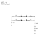
- Fig. 18 is a circuit diagram illustrating a conventional example of the automobile LED driving device.
- a switch 201 is turned ON when turning ON the tail lump and the switch 202 is turned OFF.
- a current I1 flows from a battery 100 to a light emitting diode row 600 via a switch 201, a diode 301, a resistor 401, and a resistor 500.
- the switch 201 is turned OFF and the switch 202 is turned ON.
- a current I2 flows from the battery 100 to the light emitting diode row 600 via the switch 202, the diode 302, the resistor 402, and the resistor 500.
- the resistor 402 has a smaller resistance than the resistor 401. Accordingly, the current 12 flowing when turning ON the brake lump becomes larger current value than the current I1 flowing when turning ON the tail lump, the light emitting diode row 600 emits the light brighter when turning ON the brake lump than when turning ON the tail lump.
- Japanese patent publication No. 2006-313808 can be listed.
- a purpose of the invention is to provide an automobile LED driving device to adjust an output current to the automobile LED easily and highly accurately.
- an automobile LED driving device in accordance with the invention includes a current setting portion to set multiple reference currents independently from one another for multiple respective current setting resistors connected externally, a current controller to select one of the multiple reference currents based on a control signal provided from outside, and an output transistor to control an output current to an automobile LED connected externally based on the reference current selected by the current controller.
- Fig. 1 is a block diagram illustrating a construction example of an automobile LED driver IC in accordance with the invention.
- the automobile LED driver IC1 (referred as “IC1" below) is a semiconductor integrated circuit device including an output transistor 10, a reference voltage generator 20, a H/L mode setting portion 30, a current controller 40, a LED ground short detector 50, a LED open circuit detector 60, a protect bus controller 70 (referred as "PBUS controller 70"), and a current setting portion 80.
- IC1 semiconductor integrated circuit device including an output transistor 10, a reference voltage generator 20, a H/L mode setting portion 30, a current controller 40, a LED ground short detector 50, a LED open circuit detector 60, a protect bus controller 70 (referred as "PBUS controller 70"), and a current setting portion 80.
- PBUS controller 70 protect bus controller 70
- the IC1 includes external terminals T1 to T7.
- the external terminal T1 is a turn-ON signal input terminal (VIN terminal).
- the external terminal T2 is a brake light input terminal (STOP terminal).
- the output terminal T3 is an abnormality detection input/output terminal (PBUS terminal).
- the external terminal T4 is a current setting terminal for L-mode (ISETL terminal).
- the external terminal T5 is a current setting terminal for H-mode (ISETH terminal).
- the terminal T6 is a ground terminal (GND terminal).
- the external terminal T7 is a current output terminal (IOUT terminal).
- a battery E1,switches SW1 and SW2, diodes D1to D3, a zener diode ZD1, a capacitor C1, a pull up resister R1, current setting resisters RL and RH, and a light emitting diode row LED1 are connected to the IC1 externally.
- the positive terminal of the battery E1 is connected to respective first terminals of the switches SW1 and SW2.
- the negative terminal of the battery E1 is connected to the ground terminal.
- the second terminal of the switch SW1 is connected to the anode of the diode D1.
- the second terminal of the switch SW2 is connected to respective anodes of the diodes D2 and D3.
- the cathodes of the diode D1and D2 are connected to the external terminal T1 respectively.
- the cathode of the diode D3 is connected to the external terminal T2.
- the cathode of the zener diode ZD1 is connected to the external terminal T1.
- the anode of the zener diode ZD1 is connected to the ground terminal.
- the first terminal of the capacitor C1 is connected to the external terminal T1.
- the second terminal of the capacitor C1 is connected to the ground terminal.
- the first terminal of the pull up resistor R1 is connected to the external terminal T1 (the voltage applying terminal for the input voltage VIN) or the positive terminal of the battery E1 (the voltage applying terminal for the battery voltage BAT).
- the second terminal of the pull up resistor R1 is connected to the external terminal T3.
- the first terminal of the current setting resistor RL is connected to the external terminal T4.
- the first terminal of the current setting resistor RH is connected to the external terminal T5.
- the second terminal of the current setting resistors RL and RH are connected to the ground terminal respectively.
- the external terminal T6 is connected to the ground terminal.
- the external terminal T7 is connected to the anode of the light emitting diode row LED1.
- the cathode of the light emitting diode row LED1 is connected to the ground terminal.
- the switch SW1 is turned ON when turning ON the tail lump, and the switch SW2 is turned OFF.
- the input voltage VIN is applied to the external terminal T1 from the battery E1 via the switch SW1 and the diode D1.
- the stop signal STOP provided to the external terminal T2 becomes a low level (i.e., high impedance).
- the switch SW1 is turned OFF and the switch SW2 is turned ON.
- the stop signal STOP provided to the external terminal T2 becomes a high level (i.e., battery voltage BAT).
- the output transistor 10 is a switch element to control the output current IOUT to the light emitting diode row LED1 based on a direction of the current controller 40.
- PMOS FET Metal Oxide Semiconductor
- the source and the back gate of the output transistor 10 are connected to the external terminal T1.
- the drain of the output transistor 10 is connected to the external terminal T7.
- the gate of the output transistor 10 is connected to the current controller 40.
- the reference voltage generator 20 generates a predetermined reference voltage VREF from the input voltage VIN applied to the external terminal T1.
- the H/L mode setting portion 30 generates the mode setting signal MODE based on the stop signal STOP provided to the external terminal T2 and provides it to the current controller 40.
- the current controller 40 selects either one of the first reference current IL and the second reference current IH as the reference current IREF based on the mode setting signal MODE, and drives and controls the output transistor 10 so as the output current IOUT according to the result of the selection is supplied to the light emitting diode row LED 1.
- the LED ground short detector 50 detects the ground short of the light emitting diode row LED1 (i.e., a state the external terminal T7 is shored to the ground terminal or the low voltage potential terminal which is equivalent to the ground terminal) and provides the LED ground short detection signal DET1.
- the LED ground short detection signal DET1 is a binary signal which becomes a low level when not detecting the LED ground short, and becomes a high level when detecting the LED ground short.
- the LED open circuit detector 60 detects the open circuit of the light emitting diode row LED1 (i.e., a state where the external terminal T7 is disconnected to the light emitting diode row LED1) and provides the LED open circuit detection signal DET2.
- the LED open circuit detection signal DET2 is a binary signal which becomes a low level when not detecting the LED open circuit, and becomes a high level when detecting the LED open circuit.
- PBUS controller 70 generates the protect bus signal PBUS according to with or without the detection of the abnormality, and performs input/output with outside. Moreover, the PBUS controller 70 generates forcible off signal OFF based on the protect bus signal PBUS, and provides the signal to the current controller 40.
- the current setting portion 80 sets each of the first reference current IL according to the first current setting resistance RL. and the second reference current IH (IH>IL) according to the second current setting resistance RH separately.
- an over voltage protector, a thermal protector, and a ground short detector and an open circuit detector for the current setting resistors RL and RH are integrated to the IC1.
- the first characteristic of the IC1 is designed as the voltage range for the input voltage VIN is wide as 5.5V to 40V.
- the second characteristic is including the variable constant current source driver internally as the current controller 40.
- the third characteristic is including the H/L mode setting portion 30 internally.
- the fourth characteristic is including the LED open circuit detector 50 and the LED short detector 60 internally.
- the fifth characteristic is including the ground short detector and the open circuit detector for the current setting resistors RL and RH internally.
- the sixth characteristic is including the over voltage protector and the thermal protector internally.
- the seventh characteristic is including the PBUS controller 70 (a functional member to detect an output of abnormality) internally.
- the IC1 is a LED source driver IC with high withstand voltage (50V).
- the IC1 can control a constant current output of the output current IOUT.
- the IC1 can control a current switching of the output current IOUT (i.e., H/L mode switching control). Therefore, the IC1 is suitable as a driving method for driving the automobile LED of the rear lump or the white LED.
- the IC1 includes several kinds of protection functions internally (i.e., protection functions for the ground short and the open circuit of the light emitting diode row LED1, protection functions for the ground short and the open circuit of the current setting resistors RL and RH, a overvoltage protection function, a thermal protection function), it is possible to realize a high reliability.
- the PBUS controller 70 is included to the IC 1 internally, when driving the light emitting diode row by multiple drivers (i.e., using multiple of IC1s), in the case of the ground short or the open circuit occurred at light emitting diode row by accident, all line of light emitting diode rows can be turned OFF forcibly at one time.
- Fig. 2 is a circuit diagram illustrating a construction example of a H/L mode setting portion 30 and a current controller 40.
- the H/L mode setting portion 30 includes the resistors 31 to 33, a npn bipolar transistor 34, and an inverter 35.
- the first terminal of the resistor 31 is connected to the external terminal T2. Both the second terminal of the resistor 31 and the first terminal of the resistor 32 are connected to the base of the transistor 34.
- the second terminal of the resistor 32 is connected to the ground terminal.
- the first terminal of the resistor 33 is connected to the applying terminal of the reference voltage VREF.
- the second terminal of the resistor 33 is connected to the collector of the transistor 34.
- the emitter of the transistor 34 is connected to the ground terminal.
- the input terminal of the inverter 35 is connected to the collector of the transistor 34.
- the output terminal of the inverter 35 is connected to the current controller 40 (i.e., to be more concrete, the control terminal of the selector 42 described later) which functions as an output terminal of the mode setting signal MODE.
- the H/L mode setting portion 30 functions as a level shifter to shift the voltage level of the stop signal STOP and generates the mode setting signal MODE.
- the current controller 40 includes the PMOS FET 41 and the selector 42.
- the source and the back gate of the transistor 41 are connected to the external terminal T1.
- the gate of the transistor 41 is connected to the drain of the transistor 41 with the gate of the output transistor 10.
- the drain of the transistor 41 is connected to the common terminal (i.e., an input terminal of the reference current IREF) of the selector 42.
- the first selection terminal (L) of the selector 42 is connected to the input terminal of the first reference current IL.
- the second selection terminal (H) of the selector 42 is connected to the input terminal of the second reference current IH.
- the control signal of the selector 42 is connected to the voltage applying terminal of the mode setting signal MODE (i.e., the output terminal of the inverter 35).
- the selector 42 selects either one of the first reference current IL (i.e., low current) and the second reference current IH (i.e., high current) as the reference current IREF based on the mode setting signal MODE (i.e., furthermore, the stop signal STOP according to the light ON/OFF state of the brake lump).
- the selector 42 connects the first selection terminal (L) with the common terminal when the mode setting signal MODE is low, then selecting the first reference current IL as the reference current IREF.
- the selector 42 connects the second selection terminal (H) with common terminal when the mode setting signal MODE is a high level, then the second reference current IH is selected as the reference current IREF.
- the transistor 41 is referred as the input transistor 41 properly.
- the first reference current IL i.e., low current
- the second reference current IH i.e., high current
- the light emitting diode row LED1 emits the brighter light when turning ON the brake lump than turning ON the tail lump.
- both of the output transistor 10 and the input transistor 41 are designed as high withstand voltage elements which can withstand a voltage potential difference with the input voltage VIN and the ground voltage GND.
- a source driver using a high withstand voltage element is included to the IC1 internally.
- a fluctuation caused by the forward drop voltage VF across the light emitting diode row LED1 and a discrepancy of the output current IOUT caused by a gap of the input voltage VIN can be controlled, it is not required select defective LED in a manufacturing process, furthermore, reduction of substrates or simplification of product design can be realized.
- the IC1 because an occupying area on the substrate can be reduced compared to the conventional construction which uses discrete components, a flexibility of a layout can be improved and design for the automobile can be improved.
- the IC1 further includes a bias portion 90 to equalize the source-drain voltage VDS1 of the input transistor 41 and the source-drain voltage VDS2 of the output transistor 10.
- Fig. 3 is a circuit diagram illustrating a construction example of the bias portion 90.
- the bias portion 90 of this construction example includes PMOS FETs 91 and 92, and the operational amplifiers 93 and 94.
- the source and the back gate of the transistor 91 are connected to the drain of the transistor 41.
- the drain of the transistor 91 is connected to the input terminal of the reference current IREF.
- the gate of the transistor 91 is connected to the output terminal of the operational amplifier 93.
- the source and back gate of the transistor 92 is connected to the drain of the output transistor 10.
- the drain of the transistor 92 is connected to the external terminal T7.
- the gate of the transistor 92 is connected to the output terminal of the operational amplifier 94.
- the inverting input terminal (-) of the operational amplifier 93 is connected to the source of the transistor 91.
- the inverting input terminal (-) of the operational amplifier 94 is connected to the source of the transistor 92.
- both the operational amplifiers 93 and 94 are made of high withstand voltage element which can withstand a voltage potential difference between the input voltage VIN and the ground voltage GND.
- Fig. 4 is a circuit diagram illustrating a first construction example of the current setting portion 80.
- the current setting portion 80 in accordance with the first construction example includes the NMOS FETs 81 and 82 and the operational amplifiers 83 and 84.
- the source and the back gate of the transistor 81 are connected to the external terminal T4.
- the drain of the transistor 81 is connected to the current controller 40 as the output terminal of the first reference current IL.
- the gate of the transistor 81 is connected to the output terminal of the operational amplifier 83.
- the source and the back gate of the transistor 82 are connected to the external terminal T5.
- the drain of the transistor 82 is connected to the current controller 40 as the output terminal of the second reference current IH.
- the gate of the transistor 82 is connected to the output terminal of the operational amplifier 84.
- the non-inverting input terminal (+) of the operational amplifier 83 is connected to the voltage applying terminal of the predetermined bias voltage VB.
- the inverting input terminal (-) of the operational amplifier 83 is connected to the source of the transistor 81.
- the non-inverting input terminal (+) of the operational amplifier 84 is connected to the voltage applying terminal of the predetermined bias voltage VB.
- the inverting input terminal (-) of the amplifier 84 is connected to the source of the transistor 82.
- Fig. 5 is a R/I correlation diagram illustrating a first current setting characteristic.
- Fig. 6 is a circuit diagram illustrating a second construction example of the current setting portion 80.
- the current setting portion 80 in accordance with the second construction example includes the constant current sources 85 and 86 (constant current value : IREF) and the resistors 87 and 88 (resistance: R).
- the source and the back gate of the transistor 81 are connected to the ground terminal via the resistor 87, not via the external terminal T4.
- the drain of the transistor 81 is connected to the current controller 40 as the output terminal of the first reference current IL.
- the gate of the transistor 81 is connected to the output terminal of the operational amplifier 83.
- the source and the back gate of the transistor 82 are connected to the ground terminal via the resistor 88, not via the external terminal T5.
- the drain of the transistor 82 is connected to the current controller 40 as the output terminal of the second reference current IH.
- the gate of the transistor. 82 is connected to the output terminal of the operational amplifier 84.
- the non-inverting input terminal (+) of the operational amplifier 83 is connected to the external terminal T4, not to the voltage applying terminal of the bias voltage VB.
- the inverting input terminal (-) of the amplifier 83 is connected to the source of the transistor 81.
- the non-inverting input terminal (+) of the operational amplifier 84 is connected to the external terminal T5, not to the voltage applying terminal of the bias voltage VB.
- the inverting input terminal (-) of the amplifier 84 is connected to the source of the transistor 82.
- the constant current source 85 is connected between the voltage applying terminal of the reference voltage VREF and the external terminal T4.
- the constant current source 86 is connected between the voltage applyting terminal of the reference voltage VREF and the external terminal T5.
- Fig. 7 is a R/I correlation diagram illustrating a second current setting characteristic. Accordingly, with respect to the current setting portion 80 in accordance with the second construction example, by connecting the negative characteristic thermister [Negative Temperature Coefficient] to each of the current setting resistors RL and RH in parallel, the higher the surrounding temperature becomes, the first reference current IL and the second reference current IH can be reduced. Therefore, it is possible to design a temperature derating of the output current IOUT.
- Fig. 8 is a circuit diagram illustrating a construction example of the PBUS controller 70.
- the PBUS controller 70 this construction example includes the resistors 71 to 73, the npn bipolar transistor 74, the diode 75, the NMOS FET 76, and the logical sum operation circuit 77.
- the first terminal of the resistor 71 is connected to the external terminal T3.
- the second terminal of the resistor 71 and the first terminal of the resistor 72 are connected to the base of the transistor 74.
- the second terminal of the resistor 72 is connected to the ground terminal.
- the first terminal of the resistor 73 is connected to the voltage applying terminal of the reference voltage VREF.
- the second terminal of the resistor 73 is connected to the collector of the transistor 74.
- the emitter of the transistor 74 is connected to the ground.
- the anode of the diode 75 is connected to the collector of the transistor 74.
- the cathode of the diode 75 is connected to the current controller 40 or the bias portion 90 as the output terminal of the forcible off signal OFF.
- the drain of the transistor 76 is connected to the external terminal T3.
- the source and the back gate of the transistor 76 are connected to the ground terminal.
- the gate of the transistor 76 is connected to the output terminal of the logical sum operational circuit 77.
- the first input terminal of the logical sum operational circuit 77 is connected to the input terminal of the LED ground short detection signal DET1.
- the second input terminal of the logical sum operation circuit 77 is connected to the input terminal of the LED open circuit detection signal DET2.
- other abnormality detection signals can be provided to the logical sum operational circuit 77 (i.e., the ground short detection signal of the current setting resistors RL and R-H or the open circuit detection signal).
- the PBUS controller 70 of the aforementioned construction sets the forcible off signal OFF to a low level when the protect bus signal PBUS applied to the external terminal T3 is a high level (i.e., a logic level when not detecting the abnormality), on the other hand, sets the forcible off signal OFF to a high level when the protect bus signal PBUS is a low level (i.e., a logic level when detecting the abnormality).
- the resistors 71 to 73, the transistor 74, and the diode 75 functions as a signal input circuit to generate the forcible off signal OFF according to receiving the protect bus signal PBUS.
- the forcible off signal OFF is provided to the current controller 40 or the bias portion 90, when the forcible off signal OFF becomes a high level (i.e., a logic level when detecting the abnormality), the supply of the output current IOUT is turned OFF forcibly.
- the protect bus signal PBUS when at least either one of the LED ground short detection signal DET1 and the LED open circuit detection signal DET2 is at a high level (i.e., a logic level when detecting the abnormality), the protect bus signal PBUS is set at a low level (i.e., a logic level when detecting the abnormality).
- the transistor 76 and the logical sum operational circuit 77 functions as a signal output circuit with open drain form to switch the protect bus signal PBUS to a low level (i.e., a logic level when detecting the abnormality).
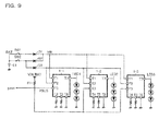
- Fig. 9 is an application diagram illustrating an application example of the protect bus signal PBUS.
- the PBUS controller 70 is included in the IC internally, for example, as illustrated in Fig. 9 , when driving three lines of the light emitting diode rows LED1 to LED3 by using three driving devices IC1-1 to IC1-3, in case of the ground short or the open circuit are occurred to some light emitting diode row, it is possible to forcibly turn OFF the all lines of the light emitting diode rows LED1 to LED3 at one time. Accordingly, at the testing process, it is possible to select all lines of the light emitting diode rows LED1 to LED3 at once. Moreover, after the mass production (i.e., after the shipment), if there is something wrong with either one of the light emitting diode rows, it is possible to detect it without delay.
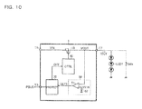
- Fig. 10 is a circuit diagram illustrating a first construction example of a LED ground short detector 50.
- the ground short detector 50 in accordance with the first construction example includes the comparator 51 and the DC voltage source 52.
- the inverting input terminal (-) of the comparator 51 is connected to the external terminal T7 (i.e., the voltage applying terminal of the output voltage VOUT).
- the non-inverting input terminal (+) of the comparator 51 is connected to the positive terminal of the DC voltage source 52 (i.e., the voltage applying terminal of the threshold voltage VTH1).
- the output terminal of the comparator 51 is connected to the PBUS controller 70 as the output terminal of the LED ground short detection signal DET1.
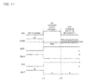
- Fig. 11 is a time chart illustrating a first LED ground short detection operation realized by the LED ground short detector 50 in accordance with the first construction example. From the top, the state of the LED ground short is occurred (i.e., ON/OFF state of the switch SWx), the output voltage VOUT, the LED ground short detection signal DET1, the protect bus signal PBUS, the forcible off signal OFF, and the output current IOUT are described in order.
- the state of the LED ground short is occurred (i.e., ON/OFF state of the switch SWx), the output voltage VOUT, the LED ground short detection signal DET1, the protect bus signal PBUS, the forcible off signal OFF, and the output current IOUT are described in order.
- the LED ground short detection signal DET1 becomes a high level and the LED ground short are detected.
- the forcible off signal OFF is set as a high level and the output current IOUT is turned OFF forcibly. Owing to this protection operation, it is possible to prevent thermal breakdown of the IC1.
- the protect bus signal PBUS is set as a low level, the abnormality is informed to the outside of the IC1.
- the LED ground short detector 50 in accordance with the first construction example, even in the case of the ground short state of the light emitting diode row LED1 is recovered at time t12 (i.e., the switch SWx: OFF), because the output voltage VOUT becomes a high impedance state and the LED ground detection signal DET1 is kept at a high level (i.e., a logic level when detecting the abnormality), the OFF state of the output current IOUT is maintained.
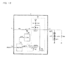
- Fig. 12 is a circuit diagram illustrating a second construction example of a LED ground short detector 50.
- the LED ground short detector 50 in accordance with the second construction example, in addition to the construction components in Fig. 10 , further including the resistor 53 (the resistance: R53), the constant current source 54 (the constant current value: 154), and the diode 55 (the forward drop voltage: V55).
- the inverting input terminal (-) of the comparator 51 is connected to the ground terminal, via the resistor 53, not via the external terminal T7, on the other hand, also connected to the voltage applying terminal of the monitor voltage VMON (i.e., a connection node between the first terminal of the constant current source 54 and the anode of the diode 55).
- VMON monitor voltage
- the cathode of the diode 55 is connected to the external terminal T7.
- the second terminal of the constant current source 54 is connected to the voltage applying terminal of the input voltage VIN.
- the output terminal of the comparator 51 is connected to the PBUS controller 70 as the output terminal of the LED ground short detection signal DET1.
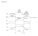
- Fig. 13 is a time chart illustrating a second LED ground short detection operation realized by the LED ground short detector 50 in accordance with the second construction example. From the top, the state of the LED ground short is occurred (i.e., ON/OFF state of the switch SWx), the monitor voltage VMON, the LED ground short detection signal DET1 , the protect bus signal PBUS, the forcible off signal OFF, and the output current IOUT are described in order.
- the state of the LED ground short is occurred (i.e., ON/OFF state of the switch SWx), the monitor voltage VMON, the LED ground short detection signal DET1 , the protect bus signal PBUS, the forcible off signal OFF, and the output current IOUT are described in order.
- the LED ground short detection signal DET1 is set as a low level (i.e., a logic level when the abnormality is not detected).
- the forcible off signal OFF is set at a high level, and the output current IOUT is turned OFF forcibly. Owing to this protection operation, it is possible to prevent the thermal breakdown of the IC1.
- the protect bus signal PBUS is set as a low level and the abnormality is informed to the outside of the IC1.
- the constant current provided from the constant current source 54 flows into the ground terminal via the light emitting diode row LED1, and the forward drop voltage VF is generated across the light emitting diode row LED1.
- the LED ground short detection signal DET1 is lowered to a low level (i.e., a logic level when not detecting the abnormality state), and the output current IOUT is recovered to ON state automatically.
- the LED ground short detector 50 in accordance with the second construction example includes a ground short recover circuit (i.e., the resistor 53, the constant current source 54, and the diode 55) to generate the forward drop voltage VF1 I by flowing small constant current 154 to the light emitting diode row LED1 when recovering from the LED ground short.
- a ground short recover circuit i.e., the resistor 53, the constant current source 54, and the diode 55
- the supply operation of the output current IOUT can be resumed automatically when recovering from the LED ground short without waiting the recover signal from outside of the IC.
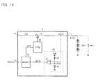
- Fig. 14 is a circuit diagram illustrating a first construction example of the LED open circuit detector 60.
- the LED open circuit detector 60 in accordance with the first construction example includes the comparator 61, the resistor 62, and the constant current source 63.
- the non-inverting input terminal (+) of the comparator 61 is connected to the external terminal T7 (i.e., a voltage applying terminal of the output voltage VOUT).
- the inverting input terminal (-) of the comparator 61 is connected to the voltage applying terminal of the input voltage VIN via the resistor 62, on the other hand, also connected to the ground terminal via the constant current source 63.
- the output terminal of the comparator 61 is connected to the PBUS controller 70 as the output terminal of the LED open circuit detection signal DET2.
- the LED open circuit detection signal DET2 becomes a high level and the LED open circuit is detected.
- the protect bus signal PBUS is lowered and an abnormality is informed to outside of the IC1
- the forcible turn OFF of the output transistor 10 is not performed different from when detecting the LED ground short. It is because the input voltage VIN is being kept applied to the external terminal T7 and to maintain the detection state of the LED open circuit.
- the LED open circuit detector 60 in accordance with the first construction example may causes a false detection of the LED open circuit when the threshold voltage VTH2 becomes smaller than aiming voltage during the low voltage (i.e., when the input voltage VIN is low).
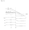
- Fig. 15 is a time chart illustrating a false detection operation of the LED detector 60 in accordance with the first construction example. From the top, the input voltage VIN, the threshold voltage VTH2, the forward drop voltages VF1 to VF3 of the light emitting diode rows LED1 to LED3 (VF1> VF2> VF3), the protect bus signal PBUS, and the currents IF1 to IF3 which flow the light emitting diode rows LED1 to LED3 respectively are described. In other words, in Fig. 15 , the situation where three lines of the light emitting diode rows LED1 to LED3 driven by three ICs IC1-1 to IC1-3 is described in order.
- the threshold voltage VTH2 begins to be lowered accordingly. And if the threshold voltage VTH2 become lower than the forward voltage drop VF1 of the light emitting diode row LED1 at time t32, the LED open circuit detection signal DET2 is set as a high level unintentionally, and the false detection of the LED open circuit is occurred. If this false detection occurred, based on the aforementioned protect bus function, only the light emitting diode row LED1 which occurs the LED open circuit keeps being turned ON, and other lines of the light emitting diode rows LED2 and LED3 are turned OFF.
- the tail lump of the automobile is formed with the light emitting diode rows LED to LED3, part of the tail lump is kept being turned ON and the rest are kept being turned OFF. This state is not a preferable state in terms of the safety of the automobile, some resolution is required.
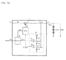
- Fig. 16 is a circuit diagram illustrating a second construction example of the LED open circuit detector 60.
- the LED open circuit detector 60 in accordance with the second construction example includes the operational amplifier 64, and the resistor 65.
- the non-inverting input terminal (+) of the comparator 61 is connected to the external terminal T7 (i.e., a voltage applying terminal of the output voltage VOUT).
- the inverting input terminal (-) of the comparator 61 is connected to the voltage applying terminal of the input voltage VIN via the resistor 62, on the other hand, also connected to the ground terminal via the resistor 65 and the constant current source 63.
- the output terminal of the comparator 6 is connected to the PBUS controller 70 as the output terminal of the LED open circuit detection signal DET2.
- the non-inverting input terminal (+) of the operational amplifier 64 is connected to the external terminal T7.
- the inverting input terminal (-) of the operational amplifier 64 is connected to the connection node between the resistor 65 and the constant current source 63.
- Fig. 17 is a time chart illustrating a false detection avoiding operation of the LED open circuit realized by the LED open circuit detector 60 in accordance with the second construction example. From the top, the input voltage VIN, the threshold voltage VTH2, the clamp voltage VCLAMP, the forward drop voltages VF1 to VF3 of the light emitting diode rows LED1 to LED3 (VF1> VF2> VF3), the protect bus signal PBUS, and the currents IF to IF3 which flow the light emitting diode rows LED1 to LED3 respectively are described in order. In other words, in Fig. 17 , same as the aforementioned Fig. 15 , the situation where three lines of the light emitting diode rows LED1 to LED3 driven by three ICs IC1-1 to IC1-3 is described.
- the current controller 40 controls and drives the output transistor 10 to reduce the output current IOUT according to the current restriction signal ICLAMP.
- the forward drop voltage VF1 is being lowered. Accordingly, it is possible to maintain the relationship as VF1 ⁇ VCLAMP, furthermore, the relationship as VF1 ⁇ VTH2 is maintained, then it becomes possible to avoid the false detection of the LED open circuit.
- both the forward drop voltage VF2 and VF3 are restricted as the clamp voltage CLAMP, all lines of the light emitting diode rows LED1 to LED3 become getting dark uniformly.
- the tail lump of the automobile is formed with the light emitting diode rows LED1 to LED3, it becomes a state where the entire tail lump is getting dark gradually. Compared to a state where only part of the tail lump is turned OFF, this state is preferable in terms of the safety of the automobile.
- the LED open circuit detector 60 in accordance with the second construction example includes the comparator 61 which generates the LED open circuit detection signal DET2 based on a comparison between the output VOUT dctectcd as the external terminal T7 to which the light emitting diode row LED1 is connected externally and the predetermined threshold voltage VTH2, the operational amplifier 64 to generate a current restriction signal ICLAMP by amplifying a subtraction between the output voltage VOUT and the clamp voltage VCLAMP.
- the current controller 40 is a construction to control the output current IOUT to the light emitting diode row LED1 as the output voltage VOUT does not to exceed the clamp voltage CLAMP based on the current restriction signal ICLAMP. According to this construction, it is possible to avoid the false detection of the LED open circuit.
- the output current IOUT can be reduced to a predetermined minimum value IMIN
- the forward drop voltages VF1 to VF3 of the light emitting diode rows LED1 to LED3 becomes higher than the threshold voltage VTH2 at time t45.
- the detection of the LED open circuit is designed to be ignored as a state where the input voltage VIN is lower than the predetermined mask voltage VMASK.
- an automobile LED driving device to control an output current to an automobile LED easily and highly accurately.
- the invention can be used appropriately to improve safety and reliability of an automobile LED driving device.
Landscapes
- Engineering & Computer Science (AREA)
- Mechanical Engineering (AREA)
- Led Devices (AREA)
- Lighting Device Outwards From Vehicle And Optical Signal (AREA)
- Circuit Arrangement For Electric Light Sources In General (AREA)
Priority Applications (3)
| Application Number | Priority Date | Filing Date | Title |
|---|---|---|---|
| EP22166991.4A EP4046870A1 (de) | 2010-09-29 | 2011-09-27 | Led-ansteuerungsvorrichtung für automobile |
| EP19189022.7A EP3626536B1 (de) | 2010-09-29 | 2011-09-27 | Led-ansteuerungsvorrichtung für automobile |
| EP20184891.8A EP3741622B8 (de) | 2010-09-29 | 2011-09-27 | Led-ansteuerungsvorrichtung für automobile |
Applications Claiming Priority (1)
| Application Number | Priority Date | Filing Date | Title |
|---|---|---|---|
| JP2010218618A JP5636241B2 (ja) | 2010-09-29 | 2010-09-29 | Led駆動装置 |
Related Child Applications (4)
| Application Number | Title | Priority Date | Filing Date |
|---|---|---|---|
| EP22166991.4A Division EP4046870A1 (de) | 2010-09-29 | 2011-09-27 | Led-ansteuerungsvorrichtung für automobile |
| EP20184891.8A Division EP3741622B8 (de) | 2010-09-29 | 2011-09-27 | Led-ansteuerungsvorrichtung für automobile |
| EP19189022.7A Division EP3626536B1 (de) | 2010-09-29 | 2011-09-27 | Led-ansteuerungsvorrichtung für automobile |
| EP19189022.7A Division-Into EP3626536B1 (de) | 2010-09-29 | 2011-09-27 | Led-ansteuerungsvorrichtung für automobile |
Publications (2)
| Publication Number | Publication Date |
|---|---|
| EP2440018A1 true EP2440018A1 (de) | 2012-04-11 |
| EP2440018B1 EP2440018B1 (de) | 2019-09-11 |
Family
ID=44862488
Family Applications (4)
| Application Number | Title | Priority Date | Filing Date |
|---|---|---|---|
| EP22166991.4A Pending EP4046870A1 (de) | 2010-09-29 | 2011-09-27 | Led-ansteuerungsvorrichtung für automobile |
| EP11182851.3A Active EP2440018B1 (de) | 2010-09-29 | 2011-09-27 | LED-Ansteuerungsvorrichtung für Automobile |
| EP20184891.8A Active EP3741622B8 (de) | 2010-09-29 | 2011-09-27 | Led-ansteuerungsvorrichtung für automobile |
| EP19189022.7A Active EP3626536B1 (de) | 2010-09-29 | 2011-09-27 | Led-ansteuerungsvorrichtung für automobile |
Family Applications Before (1)
| Application Number | Title | Priority Date | Filing Date |
|---|---|---|---|
| EP22166991.4A Pending EP4046870A1 (de) | 2010-09-29 | 2011-09-27 | Led-ansteuerungsvorrichtung für automobile |
Family Applications After (2)
| Application Number | Title | Priority Date | Filing Date |
|---|---|---|---|
| EP20184891.8A Active EP3741622B8 (de) | 2010-09-29 | 2011-09-27 | Led-ansteuerungsvorrichtung für automobile |
| EP19189022.7A Active EP3626536B1 (de) | 2010-09-29 | 2011-09-27 | Led-ansteuerungsvorrichtung für automobile |
Country Status (4)
| Country | Link |
|---|---|
| US (2) | US8754592B2 (de) |
| EP (4) | EP4046870A1 (de) |
| JP (1) | JP5636241B2 (de) |
| CN (1) | CN102431486B (de) |
Cited By (2)
| Publication number | Priority date | Publication date | Assignee | Title |
|---|---|---|---|---|
| WO2022053714A1 (de) * | 2020-09-14 | 2022-03-17 | Elmos Semiconductor Se | Kompakte steuerung für leuchtmittel im kfz |
| EP4344356A1 (de) * | 2022-09-23 | 2024-03-27 | Kaistar Lighting (Xiamen) Co., Ltd. | Leuchtdiodenansteuerungsvorrichtung mit einstellbarer dimmtiefe |
Families Citing this family (36)
| Publication number | Priority date | Publication date | Assignee | Title |
|---|---|---|---|---|
| US20120274233A1 (en) * | 2011-04-27 | 2012-11-01 | Sequoia Microelectronics Corporation | Constant current led driver |
| TWI477788B (zh) * | 2012-04-10 | 2015-03-21 | Realtek Semiconductor Corp | 偵測發光二極體短路的方法及其裝置 |
| US10621942B2 (en) * | 2012-06-06 | 2020-04-14 | Texas Instruments Incorporated | Output short circuit protection for display bias |
| US9204513B2 (en) * | 2012-10-22 | 2015-12-01 | Sharp Kabushiki Kaisha | Circuit, control program, and recording medium |
| JP6339583B2 (ja) * | 2012-11-21 | 2018-06-06 | ヴェルシテック リミテッド | カレントミラー回路及び方法 |
| TWI513363B (zh) | 2012-12-07 | 2015-12-11 | Upi Semiconductor Corp | 發光二極體的短路保護電路及其短路保護方法以及應用其之發光二極體驅動裝置 |
| CN103863172B (zh) * | 2012-12-12 | 2016-05-04 | 北汽福田汽车股份有限公司 | 一种车灯控制装置及具有其的汽车 |
| JP6143470B2 (ja) * | 2013-01-18 | 2017-06-07 | ローム株式会社 | 半導体装置 |
| TWI516906B (zh) | 2013-02-05 | 2016-01-11 | 力智電子股份有限公司 | 具有多功能參數設定的積體電路及其多功能參數設定方法 |
| DE102013202282A1 (de) * | 2013-02-13 | 2014-08-14 | Continental Automotive Gmbh | Lichtquelle und Verfahren zur Herstellung der Lichtquelle |
| JP2014156191A (ja) * | 2013-02-15 | 2014-08-28 | Ichikoh Ind Ltd | 車両用灯具点灯回路 |
| JP6331252B2 (ja) * | 2013-02-15 | 2018-05-30 | 市光工業株式会社 | 車両用灯具点灯回路 |
| CN103152949A (zh) * | 2013-03-11 | 2013-06-12 | 矽力杰半导体技术(杭州)有限公司 | 一种电容降压式led驱动器及其电容降压式led驱动方法 |
| JP5958407B2 (ja) * | 2013-04-12 | 2016-08-02 | 株式会社デンソー | Led駆動装置 |
| EP2816873B1 (de) * | 2013-06-21 | 2017-11-22 | Rohm Co., Ltd. | LED-Treiberschaltung für einen Automobilhandbremswarnleuchte mit Leerlauf- und Kurzschluss-Fehlererkennung |
| US9058762B2 (en) * | 2013-11-18 | 2015-06-16 | Sct Technology, Ltd. | Apparatus and method for driving LED display |
| JP2016009537A (ja) * | 2014-06-23 | 2016-01-18 | 三菱電機株式会社 | 光源制御装置および光源制御方法 |
| CN105472834B (zh) * | 2014-09-16 | 2018-10-26 | 株式会社小糸制作所 | 点灯电路及使用该点灯电路的车辆用灯具 |
| JP6641080B2 (ja) | 2014-11-05 | 2020-02-05 | ローム株式会社 | 発光素子駆動装置、発光装置、車両 |
| US9320117B1 (en) * | 2014-12-03 | 2016-04-19 | Kenall Manufacturing Company | Systems and methods for managing lighting settings in a lighting system |
| CN107406029B (zh) * | 2015-03-26 | 2021-03-09 | 株式会社小糸制作所 | 车辆用灯具和灯具系统 |
| CN106847191B (zh) * | 2015-12-07 | 2020-03-10 | 厦门歌乐电子企业有限公司 | 一种亮度调节电路及显示设备 |
| JP6723064B2 (ja) | 2016-05-10 | 2020-07-15 | ローム株式会社 | 地絡検出回路、異常検出回路、発光装置、車両 |
| US10426013B2 (en) | 2016-05-10 | 2019-09-24 | Rohm Co., Ltd. | Ground fault detection circuit, abnormality detection circuit, light emitting device, vehicle |
| JP6849342B2 (ja) * | 2016-08-16 | 2021-03-24 | 株式会社小糸製作所 | 点灯回路および車両用灯具 |
| US10166912B2 (en) * | 2016-08-19 | 2019-01-01 | Sl Corporation | Automotive LED driving apparatus |
| CN106548649A (zh) * | 2016-11-04 | 2017-03-29 | 上海产业技术研究院 | 一种公交电子站牌及其led灯珠故障检测方法 |
| KR102345096B1 (ko) | 2017-03-21 | 2021-12-30 | 현대자동차주식회사 | 전류 제어 장치, 그를 가지는 차량 |
| JP6951899B2 (ja) * | 2017-08-03 | 2021-10-20 | ローム株式会社 | 発光素子駆動装置 |
| CN107580395A (zh) * | 2017-09-30 | 2018-01-12 | 深圳市富满电子集团股份有限公司 | 功率控制装置、方法及系统 |
| CN108124351A (zh) * | 2017-12-25 | 2018-06-05 | 中冶建筑研究总院有限公司 | 一种垂线坐标仪 |
| CN108633142B (zh) * | 2018-07-09 | 2024-04-16 | 赛尔富电子有限公司 | 一种led灯的调光电路 |
| CN108944653B (zh) * | 2018-09-14 | 2024-05-14 | 常州瑞阳电装有限公司 | 一种全域式闪光器驱动电路 |
| KR20200109019A (ko) * | 2019-03-12 | 2020-09-22 | 엘지이노텍 주식회사 | 광원 구동장치 |
| DE112020005769T5 (de) * | 2019-11-27 | 2022-09-08 | Rohm Co. Ltd. | Led-ansteuervorrichtung, beleuchtungsvorrichtung und fahrzeugmontierte anzeigevorrichtung |
| DE112022000873T5 (de) | 2021-03-26 | 2024-02-15 | Rohm Co., Ltd. | Ansteuervorrichtung für lichtemittierende elemente, beleuchtungsvorrichtung und fahrzeug |
Citations (6)
| Publication number | Priority date | Publication date | Assignee | Title |
|---|---|---|---|---|
| US5765940A (en) * | 1995-10-31 | 1998-06-16 | Dialight Corporation | LED-illuminated stop/tail lamp assembly |
| US20020191416A1 (en) * | 1999-05-24 | 2002-12-19 | Bruce Wesson | LED light module for vehicles |
| JP2006313808A (ja) | 2005-05-09 | 2006-11-16 | Okaya Electric Ind Co Ltd | 発光ダイオードランプ |
| US20070182337A1 (en) * | 2006-02-03 | 2007-08-09 | Honeywell International Inc. | Increasing Reliability of Operation of Light Emitting Diode Arrays at Higher Operating Temperatures and its Use in the Lamps of Automobiles |
| US20090154188A1 (en) * | 2007-12-12 | 2009-06-18 | Koito Manufacturing Co., Ltd. | Vehicle lamp |
| EP2200403A1 (de) * | 2008-10-29 | 2010-06-23 | Quan Mei Technology Co. Ltd | Stromregulierte Lichtemissionsvorrichtung zur Verwendung im Fahrzeug |
Family Cites Families (16)
| Publication number | Priority date | Publication date | Assignee | Title |
|---|---|---|---|---|
| JPH09290682A (ja) * | 1996-04-26 | 1997-11-11 | Harness Sogo Kijiyutsu Kenkyusho:Kk | 自動車用ランプ制御回路 |
| US6362578B1 (en) * | 1999-12-23 | 2002-03-26 | Stmicroelectronics, Inc. | LED driver circuit and method |
| JP2004276737A (ja) * | 2003-03-14 | 2004-10-07 | Koito Mfg Co Ltd | 車両用灯具 |
| US7123136B2 (en) * | 2003-10-06 | 2006-10-17 | Anden Co., Ltd. | Indicator system having multiple LEDs |
| EP1608206B1 (de) * | 2004-06-14 | 2009-08-12 | STMicroelectronics S.r.l. | LED-Ssteuergeräte mit Lichtintensitätsänderung |
| JP2006091138A (ja) * | 2004-09-21 | 2006-04-06 | Denso Corp | 液晶表示装置 |
| JP4451376B2 (ja) * | 2005-11-04 | 2010-04-14 | 株式会社小糸製作所 | 車両用灯具の点灯制御装置 |
| US7667414B2 (en) * | 2006-05-24 | 2010-02-23 | Stanley Electric Co., Ltd. | LED lighting apparatus |
| TWI354966B (en) * | 2006-10-19 | 2011-12-21 | Richtek Technology Corp | Backlight control circuit |
| JP4943402B2 (ja) * | 2008-10-09 | 2012-05-30 | シャープ株式会社 | Led駆動回路、led照明灯具、led照明機器、及びled照明システム |
| US7952290B2 (en) * | 2008-10-09 | 2011-05-31 | Quan Mei Technology Co., Ltd. | Current-regulated light emitting device for vehicle use |
| JP2010113924A (ja) * | 2008-11-06 | 2010-05-20 | Shindengen Electric Mfg Co Ltd | Led点灯駆動回路、半導体集積回路、および照明器具 |
| US8189313B1 (en) * | 2008-12-03 | 2012-05-29 | Analog Devices, Inc. | Fault detection and handling for current sources |
| JP4864994B2 (ja) * | 2009-03-06 | 2012-02-01 | シャープ株式会社 | Led駆動回路、led照明灯具、led照明機器、及びled照明システム |
| TWI397345B (zh) * | 2009-06-19 | 2013-05-21 | Delta Electronics Inc | 發光二極體之供電電路 |
| US8084960B2 (en) * | 2009-12-30 | 2011-12-27 | O2Micro, Inc | Circuits and methods for powering light source with balanced currents |
-
2010
- 2010-09-29 JP JP2010218618A patent/JP5636241B2/ja active Active
-
2011
- 2011-09-23 US US13/241,505 patent/US8754592B2/en active Active
- 2011-09-27 EP EP22166991.4A patent/EP4046870A1/de active Pending
- 2011-09-27 EP EP11182851.3A patent/EP2440018B1/de active Active
- 2011-09-27 EP EP20184891.8A patent/EP3741622B8/de active Active
- 2011-09-27 EP EP19189022.7A patent/EP3626536B1/de active Active
- 2011-09-28 CN CN201110303776.7A patent/CN102431486B/zh active Active
-
2014
- 2014-05-07 US US14/271,625 patent/US9148915B2/en active Active
Patent Citations (6)
| Publication number | Priority date | Publication date | Assignee | Title |
|---|---|---|---|---|
| US5765940A (en) * | 1995-10-31 | 1998-06-16 | Dialight Corporation | LED-illuminated stop/tail lamp assembly |
| US20020191416A1 (en) * | 1999-05-24 | 2002-12-19 | Bruce Wesson | LED light module for vehicles |
| JP2006313808A (ja) | 2005-05-09 | 2006-11-16 | Okaya Electric Ind Co Ltd | 発光ダイオードランプ |
| US20070182337A1 (en) * | 2006-02-03 | 2007-08-09 | Honeywell International Inc. | Increasing Reliability of Operation of Light Emitting Diode Arrays at Higher Operating Temperatures and its Use in the Lamps of Automobiles |
| US20090154188A1 (en) * | 2007-12-12 | 2009-06-18 | Koito Manufacturing Co., Ltd. | Vehicle lamp |
| EP2200403A1 (de) * | 2008-10-29 | 2010-06-23 | Quan Mei Technology Co. Ltd | Stromregulierte Lichtemissionsvorrichtung zur Verwendung im Fahrzeug |
Cited By (2)
| Publication number | Priority date | Publication date | Assignee | Title |
|---|---|---|---|---|
| WO2022053714A1 (de) * | 2020-09-14 | 2022-03-17 | Elmos Semiconductor Se | Kompakte steuerung für leuchtmittel im kfz |
| EP4344356A1 (de) * | 2022-09-23 | 2024-03-27 | Kaistar Lighting (Xiamen) Co., Ltd. | Leuchtdiodenansteuerungsvorrichtung mit einstellbarer dimmtiefe |
Also Published As
| Publication number | Publication date |
|---|---|
| EP3626536A1 (de) | 2020-03-25 |
| EP2440018B1 (de) | 2019-09-11 |
| US20140239851A1 (en) | 2014-08-28 |
| JP5636241B2 (ja) | 2014-12-03 |
| EP4046870A1 (de) | 2022-08-24 |
| US20120074845A1 (en) | 2012-03-29 |
| CN102431486B (zh) | 2016-02-17 |
| JP2012071712A (ja) | 2012-04-12 |
| EP3626536B1 (de) | 2021-04-14 |
| CN102431486A (zh) | 2012-05-02 |
| EP3741622B1 (de) | 2022-04-13 |
| EP3741622B8 (de) | 2022-08-03 |
| US8754592B2 (en) | 2014-06-17 |
| EP3741622A1 (de) | 2020-11-25 |
| US9148915B2 (en) | 2015-09-29 |
Similar Documents
| Publication | Publication Date | Title |
|---|---|---|
| EP2440018B1 (de) | LED-Ansteuerungsvorrichtung für Automobile | |
| US7839099B2 (en) | LED control circuit and method therefor | |
| US8289669B2 (en) | Semiconductor device including over voltage protection circuit having gate discharge circuit operated based on temperature and voltage as to output transistor | |
| US8324816B2 (en) | LED driving circuit | |
| US20140292201A1 (en) | Driver Circuit for Efficiently Driving a Large Number of LEDs | |
| US10477643B2 (en) | Lighting device and vehicle | |
| US10405386B2 (en) | Light emitting element driving apparatus and driving method thereof | |
| US20140252950A1 (en) | Semiconductor light source lighting circuit and vehicular lamp | |
| US20100177127A1 (en) | Led driving circuit, semiconductor element and image display device | |
| US20140218657A1 (en) | Control circuit for light emitting apparatus | |
| US8143808B2 (en) | Circuit for a motor vehicle, in particular for actuating a lighting device | |
| JP2008198915A (ja) | 発光装置 | |
| EP2675246A2 (de) | Halbleiterlichtquellensteuerungsvorrichtung | |
| KR101208325B1 (ko) | 전류 감지 회로 및 그 형성 방법 | |
| JP2010015728A (ja) | バックライト調光制御装置 | |
| US20110163693A1 (en) | Circuit arrangement and method for operating at least one led | |
| JP6951899B2 (ja) | 発光素子駆動装置 | |
| WO2022097430A1 (ja) | 発光素子駆動用半導体集積回路、発光素子駆動装置、発光装置、車両 | |
| JP2009211210A (ja) | 電源回路装置および電子機器 | |
| JP7249887B2 (ja) | Led制御装置、led駆動装置、及び表示装置 | |
| CN112369124B (zh) | 光源驱动装置及其方法 | |
| JP2008269066A (ja) | 電源回路および電源供給回路システム |
Legal Events
| Date | Code | Title | Description |
|---|---|---|---|
| AK | Designated contracting states |
Kind code of ref document: A1 Designated state(s): AL AT BE BG CH CY CZ DE DK EE ES FI FR GB GR HR HU IE IS IT LI LT LU LV MC MK MT NL NO PL PT RO RS SE SI SK SM TR |
|
| AX | Request for extension of the european patent |
Extension state: BA ME |
|
| PUAI | Public reference made under article 153(3) epc to a published international application that has entered the european phase |
Free format text: ORIGINAL CODE: 0009012 |
|
| 17P | Request for examination filed |
Effective date: 20121010 |
|
| 17Q | First examination report despatched |
Effective date: 20121207 |
|
| STAA | Information on the status of an ep patent application or granted ep patent |
Free format text: STATUS: EXAMINATION IS IN PROGRESS |
|
| GRAP | Despatch of communication of intention to grant a patent |
Free format text: ORIGINAL CODE: EPIDOSNIGR1 |
|
| STAA | Information on the status of an ep patent application or granted ep patent |
Free format text: STATUS: GRANT OF PATENT IS INTENDED |
|
| INTG | Intention to grant announced |
Effective date: 20190403 |
|
| RIN1 | Information on inventor provided before grant (corrected) |
Inventor name: MIYAMOTO, KOJI Inventor name: AOKI, AKIRA |
|
| GRAS | Grant fee paid |
Free format text: ORIGINAL CODE: EPIDOSNIGR3 |
|
| GRAA | (expected) grant |
Free format text: ORIGINAL CODE: 0009210 |
|
| STAA | Information on the status of an ep patent application or granted ep patent |
Free format text: STATUS: THE PATENT HAS BEEN GRANTED |
|
| AK | Designated contracting states |
Kind code of ref document: B1 Designated state(s): AL AT BE BG CH CY CZ DE DK EE ES FI FR GB GR HR HU IE IS IT LI LT LU LV MC MK MT NL NO PL PT RO RS SE SI SK SM TR |
|
| REG | Reference to a national code |
Ref country code: GB Ref legal event code: FG4D |
|
| REG | Reference to a national code |
Ref country code: CH Ref legal event code: EP |
|
| REG | Reference to a national code |
Ref country code: AT Ref legal event code: REF Ref document number: 1180169 Country of ref document: AT Kind code of ref document: T Effective date: 20190915 |
|
| REG | Reference to a national code |
Ref country code: DE Ref legal event code: R096 Ref document number: 602011061946 Country of ref document: DE Ref country code: IE Ref legal event code: FG4D |
|
| REG | Reference to a national code |
Ref country code: DE Ref legal event code: R079 Ref document number: 602011061946 Country of ref document: DE Free format text: PREVIOUS MAIN CLASS: H05B0033080000 Ipc: H05B0045000000 |
|
| REG | Reference to a national code |
Ref country code: NL Ref legal event code: MP Effective date: 20190911 |
|
| REG | Reference to a national code |
Ref country code: LT Ref legal event code: MG4D |
|
| PG25 | Lapsed in a contracting state [announced via postgrant information from national office to epo] |
Ref country code: FI Free format text: LAPSE BECAUSE OF FAILURE TO SUBMIT A TRANSLATION OF THE DESCRIPTION OR TO PAY THE FEE WITHIN THE PRESCRIBED TIME-LIMIT Effective date: 20190911 Ref country code: SE Free format text: LAPSE BECAUSE OF FAILURE TO SUBMIT A TRANSLATION OF THE DESCRIPTION OR TO PAY THE FEE WITHIN THE PRESCRIBED TIME-LIMIT Effective date: 20190911 Ref country code: HR Free format text: LAPSE BECAUSE OF FAILURE TO SUBMIT A TRANSLATION OF THE DESCRIPTION OR TO PAY THE FEE WITHIN THE PRESCRIBED TIME-LIMIT Effective date: 20190911 Ref country code: LT Free format text: LAPSE BECAUSE OF FAILURE TO SUBMIT A TRANSLATION OF THE DESCRIPTION OR TO PAY THE FEE WITHIN THE PRESCRIBED TIME-LIMIT Effective date: 20190911 Ref country code: NO Free format text: LAPSE BECAUSE OF FAILURE TO SUBMIT A TRANSLATION OF THE DESCRIPTION OR TO PAY THE FEE WITHIN THE PRESCRIBED TIME-LIMIT Effective date: 20191211 Ref country code: BG Free format text: LAPSE BECAUSE OF FAILURE TO SUBMIT A TRANSLATION OF THE DESCRIPTION OR TO PAY THE FEE WITHIN THE PRESCRIBED TIME-LIMIT Effective date: 20191211 |
|
| PG25 | Lapsed in a contracting state [announced via postgrant information from national office to epo] |
Ref country code: AL Free format text: LAPSE BECAUSE OF FAILURE TO SUBMIT A TRANSLATION OF THE DESCRIPTION OR TO PAY THE FEE WITHIN THE PRESCRIBED TIME-LIMIT Effective date: 20190911 Ref country code: RS Free format text: LAPSE BECAUSE OF FAILURE TO SUBMIT A TRANSLATION OF THE DESCRIPTION OR TO PAY THE FEE WITHIN THE PRESCRIBED TIME-LIMIT Effective date: 20190911 Ref country code: LV Free format text: LAPSE BECAUSE OF FAILURE TO SUBMIT A TRANSLATION OF THE DESCRIPTION OR TO PAY THE FEE WITHIN THE PRESCRIBED TIME-LIMIT Effective date: 20190911 Ref country code: GR Free format text: LAPSE BECAUSE OF FAILURE TO SUBMIT A TRANSLATION OF THE DESCRIPTION OR TO PAY THE FEE WITHIN THE PRESCRIBED TIME-LIMIT Effective date: 20191212 Ref country code: ES Free format text: LAPSE BECAUSE OF FAILURE TO SUBMIT A TRANSLATION OF THE DESCRIPTION OR TO PAY THE FEE WITHIN THE PRESCRIBED TIME-LIMIT Effective date: 20190911 |
|
| REG | Reference to a national code |
Ref country code: AT Ref legal event code: MK05 Ref document number: 1180169 Country of ref document: AT Kind code of ref document: T Effective date: 20190911 |
|
| PG25 | Lapsed in a contracting state [announced via postgrant information from national office to epo] |
Ref country code: RO Free format text: LAPSE BECAUSE OF FAILURE TO SUBMIT A TRANSLATION OF THE DESCRIPTION OR TO PAY THE FEE WITHIN THE PRESCRIBED TIME-LIMIT Effective date: 20190911 Ref country code: PL Free format text: LAPSE BECAUSE OF FAILURE TO SUBMIT A TRANSLATION OF THE DESCRIPTION OR TO PAY THE FEE WITHIN THE PRESCRIBED TIME-LIMIT Effective date: 20190911 Ref country code: PT Free format text: LAPSE BECAUSE OF FAILURE TO SUBMIT A TRANSLATION OF THE DESCRIPTION OR TO PAY THE FEE WITHIN THE PRESCRIBED TIME-LIMIT Effective date: 20200113 Ref country code: AT Free format text: LAPSE BECAUSE OF FAILURE TO SUBMIT A TRANSLATION OF THE DESCRIPTION OR TO PAY THE FEE WITHIN THE PRESCRIBED TIME-LIMIT Effective date: 20190911 Ref country code: NL Free format text: LAPSE BECAUSE OF FAILURE TO SUBMIT A TRANSLATION OF THE DESCRIPTION OR TO PAY THE FEE WITHIN THE PRESCRIBED TIME-LIMIT Effective date: 20190911 Ref country code: EE Free format text: LAPSE BECAUSE OF FAILURE TO SUBMIT A TRANSLATION OF THE DESCRIPTION OR TO PAY THE FEE WITHIN THE PRESCRIBED TIME-LIMIT Effective date: 20190911 Ref country code: IT Free format text: LAPSE BECAUSE OF FAILURE TO SUBMIT A TRANSLATION OF THE DESCRIPTION OR TO PAY THE FEE WITHIN THE PRESCRIBED TIME-LIMIT Effective date: 20190911 |
|
| PG25 | Lapsed in a contracting state [announced via postgrant information from national office to epo] |
Ref country code: CZ Free format text: LAPSE BECAUSE OF FAILURE TO SUBMIT A TRANSLATION OF THE DESCRIPTION OR TO PAY THE FEE WITHIN THE PRESCRIBED TIME-LIMIT Effective date: 20190911 Ref country code: SM Free format text: LAPSE BECAUSE OF FAILURE TO SUBMIT A TRANSLATION OF THE DESCRIPTION OR TO PAY THE FEE WITHIN THE PRESCRIBED TIME-LIMIT Effective date: 20190911 Ref country code: SK Free format text: LAPSE BECAUSE OF FAILURE TO SUBMIT A TRANSLATION OF THE DESCRIPTION OR TO PAY THE FEE WITHIN THE PRESCRIBED TIME-LIMIT Effective date: 20190911 Ref country code: IS Free format text: LAPSE BECAUSE OF FAILURE TO SUBMIT A TRANSLATION OF THE DESCRIPTION OR TO PAY THE FEE WITHIN THE PRESCRIBED TIME-LIMIT Effective date: 20200224 |
|
| REG | Reference to a national code |
Ref country code: CH Ref legal event code: PL |
|
| REG | Reference to a national code |
Ref country code: DE Ref legal event code: R097 Ref document number: 602011061946 Country of ref document: DE |
|
| PLBE | No opposition filed within time limit |
Free format text: ORIGINAL CODE: 0009261 |
|
| STAA | Information on the status of an ep patent application or granted ep patent |
Free format text: STATUS: NO OPPOSITION FILED WITHIN TIME LIMIT |
|
| PG2D | Information on lapse in contracting state deleted |
Ref country code: IS |
|
| PG25 | Lapsed in a contracting state [announced via postgrant information from national office to epo] |
Ref country code: DK Free format text: LAPSE BECAUSE OF FAILURE TO SUBMIT A TRANSLATION OF THE DESCRIPTION OR TO PAY THE FEE WITHIN THE PRESCRIBED TIME-LIMIT Effective date: 20190911 Ref country code: LU Free format text: LAPSE BECAUSE OF NON-PAYMENT OF DUE FEES Effective date: 20190927 Ref country code: IE Free format text: LAPSE BECAUSE OF NON-PAYMENT OF DUE FEES Effective date: 20190927 Ref country code: CH Free format text: LAPSE BECAUSE OF NON-PAYMENT OF DUE FEES Effective date: 20190930 Ref country code: LI Free format text: LAPSE BECAUSE OF NON-PAYMENT OF DUE FEES Effective date: 20190930 Ref country code: IS Free format text: LAPSE BECAUSE OF FAILURE TO SUBMIT A TRANSLATION OF THE DESCRIPTION OR TO PAY THE FEE WITHIN THE PRESCRIBED TIME-LIMIT Effective date: 20200112 |
|
| REG | Reference to a national code |
Ref country code: BE Ref legal event code: MM Effective date: 20190930 |
|
| 26N | No opposition filed |
Effective date: 20200615 |
|
| PG25 | Lapsed in a contracting state [announced via postgrant information from national office to epo] |
Ref country code: MC Free format text: LAPSE BECAUSE OF FAILURE TO SUBMIT A TRANSLATION OF THE DESCRIPTION OR TO PAY THE FEE WITHIN THE PRESCRIBED TIME-LIMIT Effective date: 20190911 Ref country code: SI Free format text: LAPSE BECAUSE OF FAILURE TO SUBMIT A TRANSLATION OF THE DESCRIPTION OR TO PAY THE FEE WITHIN THE PRESCRIBED TIME-LIMIT Effective date: 20190911 Ref country code: BE Free format text: LAPSE BECAUSE OF NON-PAYMENT OF DUE FEES Effective date: 20190930 |
|
| GBPC | Gb: european patent ceased through non-payment of renewal fee |
Effective date: 20191211 |
|
| PG25 | Lapsed in a contracting state [announced via postgrant information from national office to epo] |
Ref country code: GB Free format text: LAPSE BECAUSE OF NON-PAYMENT OF DUE FEES Effective date: 20191211 Ref country code: FR Free format text: LAPSE BECAUSE OF NON-PAYMENT OF DUE FEES Effective date: 20191111 |
|
| PG25 | Lapsed in a contracting state [announced via postgrant information from national office to epo] |
Ref country code: CY Free format text: LAPSE BECAUSE OF FAILURE TO SUBMIT A TRANSLATION OF THE DESCRIPTION OR TO PAY THE FEE WITHIN THE PRESCRIBED TIME-LIMIT Effective date: 20190911 |
|
| PG25 | Lapsed in a contracting state [announced via postgrant information from national office to epo] |
Ref country code: MT Free format text: LAPSE BECAUSE OF FAILURE TO SUBMIT A TRANSLATION OF THE DESCRIPTION OR TO PAY THE FEE WITHIN THE PRESCRIBED TIME-LIMIT Effective date: 20190911 Ref country code: HU Free format text: LAPSE BECAUSE OF FAILURE TO SUBMIT A TRANSLATION OF THE DESCRIPTION OR TO PAY THE FEE WITHIN THE PRESCRIBED TIME-LIMIT; INVALID AB INITIO Effective date: 20110927 |
|
| PG25 | Lapsed in a contracting state [announced via postgrant information from national office to epo] |
Ref country code: TR Free format text: LAPSE BECAUSE OF FAILURE TO SUBMIT A TRANSLATION OF THE DESCRIPTION OR TO PAY THE FEE WITHIN THE PRESCRIBED TIME-LIMIT Effective date: 20190911 |
|
| PG25 | Lapsed in a contracting state [announced via postgrant information from national office to epo] |
Ref country code: MK Free format text: LAPSE BECAUSE OF FAILURE TO SUBMIT A TRANSLATION OF THE DESCRIPTION OR TO PAY THE FEE WITHIN THE PRESCRIBED TIME-LIMIT Effective date: 20190911 |
|
| P01 | Opt-out of the competence of the unified patent court (upc) registered |
Effective date: 20230512 |
|
| PGFP | Annual fee paid to national office [announced via postgrant information from national office to epo] |
Ref country code: DE Payment date: 20230802 Year of fee payment: 13 |