EP2412040B1 - Dünnschichtverkapselung für ein optoelektronisches bauelement, verfahren zu dessen herstellung und optoelektronisches bauelement - Google Patents
Dünnschichtverkapselung für ein optoelektronisches bauelement, verfahren zu dessen herstellung und optoelektronisches bauelement Download PDFInfo
- Publication number
- EP2412040B1 EP2412040B1 EP10710030.7A EP10710030A EP2412040B1 EP 2412040 B1 EP2412040 B1 EP 2412040B1 EP 10710030 A EP10710030 A EP 10710030A EP 2412040 B1 EP2412040 B1 EP 2412040B1
- Authority
- EP
- European Patent Office
- Prior art keywords
- layer
- ald
- thin
- layers
- optoelectronic component
- Prior art date
- Legal status (The legal status is an assumption and is not a legal conclusion. Google has not performed a legal analysis and makes no representation as to the accuracy of the status listed.)
- Active
Links
Images


Classifications
-
- H—ELECTRICITY
- H10—SEMICONDUCTOR DEVICES; ELECTRIC SOLID-STATE DEVICES NOT OTHERWISE PROVIDED FOR
- H10K—ORGANIC ELECTRIC SOLID-STATE DEVICES
- H10K50/00—Organic light-emitting devices
- H10K50/80—Constructional details
- H10K50/84—Passivation; Containers; Encapsulations
- H10K50/844—Encapsulations
- H10K50/8445—Encapsulations multilayered coatings having a repetitive structure, e.g. having multiple organic-inorganic bilayers
-
- C—CHEMISTRY; METALLURGY
- C23—COATING METALLIC MATERIAL; COATING MATERIAL WITH METALLIC MATERIAL; CHEMICAL SURFACE TREATMENT; DIFFUSION TREATMENT OF METALLIC MATERIAL; COATING BY VACUUM EVAPORATION, BY SPUTTERING, BY ION IMPLANTATION OR BY CHEMICAL VAPOUR DEPOSITION, IN GENERAL; INHIBITING CORROSION OF METALLIC MATERIAL OR INCRUSTATION IN GENERAL
- C23C—COATING METALLIC MATERIAL; COATING MATERIAL WITH METALLIC MATERIAL; SURFACE TREATMENT OF METALLIC MATERIAL BY DIFFUSION INTO THE SURFACE, BY CHEMICAL CONVERSION OR SUBSTITUTION; COATING BY VACUUM EVAPORATION, BY SPUTTERING, BY ION IMPLANTATION OR BY CHEMICAL VAPOUR DEPOSITION, IN GENERAL
- C23C16/00—Chemical coating by decomposition of gaseous compounds, without leaving reaction products of surface material in the coating, i.e. chemical vapour deposition [CVD] processes
- C23C16/44—Chemical coating by decomposition of gaseous compounds, without leaving reaction products of surface material in the coating, i.e. chemical vapour deposition [CVD] processes characterised by the method of coating
- C23C16/455—Chemical coating by decomposition of gaseous compounds, without leaving reaction products of surface material in the coating, i.e. chemical vapour deposition [CVD] processes characterised by the method of coating characterised by the method used for introducing gases into reaction chamber or for modifying gas flows in reaction chamber
- C23C16/45523—Pulsed gas flow or change of composition over time
- C23C16/45525—Atomic layer deposition [ALD]
-
- H—ELECTRICITY
- H10—SEMICONDUCTOR DEVICES; ELECTRIC SOLID-STATE DEVICES NOT OTHERWISE PROVIDED FOR
- H10K—ORGANIC ELECTRIC SOLID-STATE DEVICES
- H10K30/00—Organic devices sensitive to infrared radiation, light, electromagnetic radiation of shorter wavelength or corpuscular radiation
- H10K30/10—Organic devices sensitive to infrared radiation, light, electromagnetic radiation of shorter wavelength or corpuscular radiation comprising heterojunctions between organic semiconductors and inorganic semiconductors
- H10K30/15—Sensitised wide-bandgap semiconductor devices, e.g. dye-sensitised TiO2
-
- H—ELECTRICITY
- H10—SEMICONDUCTOR DEVICES; ELECTRIC SOLID-STATE DEVICES NOT OTHERWISE PROVIDED FOR
- H10K—ORGANIC ELECTRIC SOLID-STATE DEVICES
- H10K30/00—Organic devices sensitive to infrared radiation, light, electromagnetic radiation of shorter wavelength or corpuscular radiation
- H10K30/80—Constructional details
- H10K30/88—Passivation; Containers; Encapsulations
-
- H—ELECTRICITY
- H10—SEMICONDUCTOR DEVICES; ELECTRIC SOLID-STATE DEVICES NOT OTHERWISE PROVIDED FOR
- H10K—ORGANIC ELECTRIC SOLID-STATE DEVICES
- H10K71/00—Manufacture or treatment specially adapted for the organic devices covered by this subclass
-
- Y—GENERAL TAGGING OF NEW TECHNOLOGICAL DEVELOPMENTS; GENERAL TAGGING OF CROSS-SECTIONAL TECHNOLOGIES SPANNING OVER SEVERAL SECTIONS OF THE IPC; TECHNICAL SUBJECTS COVERED BY FORMER USPC CROSS-REFERENCE ART COLLECTIONS [XRACs] AND DIGESTS
- Y02—TECHNOLOGIES OR APPLICATIONS FOR MITIGATION OR ADAPTATION AGAINST CLIMATE CHANGE
- Y02E—REDUCTION OF GREENHOUSE GAS [GHG] EMISSIONS, RELATED TO ENERGY GENERATION, TRANSMISSION OR DISTRIBUTION
- Y02E10/00—Energy generation through renewable energy sources
- Y02E10/50—Photovoltaic [PV] energy
- Y02E10/549—Organic PV cells
-
- Y—GENERAL TAGGING OF NEW TECHNOLOGICAL DEVELOPMENTS; GENERAL TAGGING OF CROSS-SECTIONAL TECHNOLOGIES SPANNING OVER SEVERAL SECTIONS OF THE IPC; TECHNICAL SUBJECTS COVERED BY FORMER USPC CROSS-REFERENCE ART COLLECTIONS [XRACs] AND DIGESTS
- Y02—TECHNOLOGIES OR APPLICATIONS FOR MITIGATION OR ADAPTATION AGAINST CLIMATE CHANGE
- Y02P—CLIMATE CHANGE MITIGATION TECHNOLOGIES IN THE PRODUCTION OR PROCESSING OF GOODS
- Y02P70/00—Climate change mitigation technologies in the production process for final industrial or consumer products
- Y02P70/50—Manufacturing or production processes characterised by the final manufactured product
Definitions
- the present application relates to a thin-film encapsulation for an optoelectronic component, a method for its production and an optoelectronic component.
- Opto-electronic devices and especially those having an organic functional material, such as organic light-emitting diodes (OLEDs), are extremely sensitive to moisture and oxygen.
- OLEDs organic light-emitting diodes
- OLEDs are usually encapsulated in a costly manner with glass cavities which are glued onto the component.
- thin-film encapsulations with thin layers are known, which seal the component against moisture and oxygen.
- Such a thin-layer encapsulation is for example in the applications DE 10 2008 031 405 .
- the thin-layer encapsulation described herein has the particular disadvantage of having only a low optical transmission for visible light.
- US 2006/017383 A1 discloses a thin film encapsulation for an optoelectronic device having a layer sequence comprising the following layers: a first ALD layer deposited by atomic layer deposition consisting of titanium oxide, and a second ALD layer deposited by atomic layer deposition, which consists of aluminum oxide, wherein the layer sequence comprises a plurality at first ALD layers and second ALD layers that repeat periodically.
- the object of the present invention is to specify an improved thin-film encapsulation for an optoelectronic component.
- the thin-layer encapsulation should have a good optical transmission for visible light. It is another object of the present application to provide a method for producing the thin-layer encapsulation and an optoelectronic component with such a thin-layer encapsulation.
- Thin-layer encapsulation is understood here to mean a device which is suitable for forming a barrier to atmospheric substances, in particular to moisture and oxygen.
- the thin-layer encapsulation is designed so that it can be penetrated by atmospheric substances such as water or oxygen, at most at very low levels.
- this barrier effect is essentially produced by thin layers which form part of the thin-layer encapsulation.
- the layers of the thin-layer encapsulation generally have a thickness of less than or equal to a few 100 nm.
- the thin-layer encapsulation consists of the thin layers suitable for the Barrier effect of the Dünn fürverkapselung are responsible.
- a thin-layer encapsulation for an optoelectronic component with good visible light transmission has a layer sequence comprising the following layers: a first ALD layer deposited by atomic layer deposition, which consists of titanium oxide, and a second ALD layer deposited by atomic layer deposition, which consists of lanthanum oxide, wherein the layer sequence comprises a plurality of first ALD layers and second ALD layers which repeat periodically and are in direct contact with each other, and an outer surface of the thin film encapsulation is formed by an ALD layer consisting of titanium oxide , It should be noted at this point that the layer sequence can have further ALD layers. Likewise, the layer sequence can have further layers, which were produced by methods other than atomic layer deposition.
- a layer sequence which has only ALD layers is also referred to herein as "nanolaminate”.
- ALD atomic layer deposition
- the surface to be coated is heated to a temperature above room temperature. Thereby, the reaction for forming the solid ALD layer can be thermally initiated.
- the temperature of the surface to be coated is usually dependent on the starting compounds.
- a plasma-less atomic layer deposition designates in the present case an ALD process for which no plasma is produced as described below, but in which the reaction of the starting compounds takes place only via the plasma phase to form the solid layer Temperature of the surface to be coated is initiated.
- the temperature of the surface to be coated is usually between 60 ° C and 120 ° C in a PLALD process, the limits being included.
- Plasma-enhanced atomic layer deposition in the present case also refers to an ALD process in which the second starting compound is supplied with the simultaneous production of a plasma, whereby the second starting compound is to be excited.
- This can - compared to a non-plasmal ALD processes - the temperature at which the surface to be coated must be heated is reduced, and the plasma generation nevertheless initiates the reaction between the starting compounds.
- the temperature of the surface to be coated is preferably less than or equal to 120 ° C., particularly preferably less than or equal to 80 ° C., for PEALD.
- a PEALD process may be advantageous if initiation of the reaction between the starting compounds requires a surface temperature at which the device to be encapsulated might be damaged.
- the first ALD layer is in direct contact with the second ALD layer.
- the first ALD layer deposited by atomic layer deposition consists of titanium oxide.
- the second deposited by atomic layer deposition ALD layer consists of lanthanum oxide.
- the ALD layers of the layer sequence are formed particularly thin, for example, they have a thickness between an atomic layer and 10 nm, wherein the limits are included. This usually contributes to a high optical transmission of the thin-layer encapsulation.
- the layer sequence of the thin-layer encapsulation comprises at least one further layer which has been deposited by thermal vapor deposition or by means of a plasma-assisted process, such as sputtering or plasma-enhanced chemical vapor deposition (PECVD).
- a plasma-assisted process such as sputtering or plasma-enhanced chemical vapor deposition (PECVD).
- Suitable materials for the further layer are: silicon nitride, silicon oxide, silicon oxynitride, indium tin oxide, indium zinc oxide, aluminum-doped zinc oxide, aluminum oxide and mixtures and alloys thereof.
- the further layer has, for example, a thickness of between 1 nm and 5 ⁇ m, the limits being included. Particularly preferably, the further layer has a thickness between 1 nm and 400 nm, again including the boundaries.
- this has a nanolaminate, to which a further layer is arranged in direct contact.
- a particularly preferred thin-layer encapsulation which ensures high optical transmission for visible light and a particularly good hermetic barrier effect, has a further layer which is applied by means of a plasma-supported process and comprises silicon nitride or consists of silicon nitride.
- the layer sequence of the thin-layer encapsulation may have a further ALD layer.
- This further ALD layer may, for example, comprise or consist of at least one of the following materials: aluminum oxide, zinc oxide, zirconium oxide, titanium oxide, hafnium oxide, lanthanum oxide.
- an outer surface of the thin-film encapsulation is formed by an ALD layer consisting of titanium oxide.
- the layers of the layer sequence are repeated periodically.
- the thin-layer encapsulation particularly preferably has a nanolaminate whose ALD layers repeat multiply or periodically within the nanolaminate. As a result, advantageously a particularly dense thin-layer encapsulation can be achieved.
- the present thin-layer encapsulation it is advantageously possible to adapt the optical properties of the thin-layer encapsulation in a desired manner by suitably selecting the individual layers, in particular with regard to the thickness and materials of the layers. For example, by a suitable selection of layer thicknesses and materials of the layers, the transmittance and the reflectivity of the thin-layer encapsulation can be adapted in a desired manner.
- a thin-layer encapsulation with an antireflection effect or with a desired degree of transmission can be achieved.
- the thin-layer encapsulation particularly preferably has a transmission for visible light which is greater than or equal to 70%. Particularly preferably, the transmission of the thin-layer encapsulation for visible light is greater than or equal to 90%.
- the present thin-film encapsulation is particularly suitable for optoelectronic components, since their optical Properties can be customized in the desired manner.
- the thin-layer encapsulation is preferably applied between the active zone and the substrate. This arrangement advantageously protects in particular the sensitive active zone.
- the thin-layer encapsulation is usually first applied to the substrate and then the active zone above the thin-layer encapsulation.
- the present thin-layer encapsulation is particularly suitable for being applied to flexible substrates, such as metal foils or plastic films, since they do not lose their flexibility due to the thin-layer encapsulation due to the small thickness of the thin-layer encapsulation.
- the thin-layer encapsulation is arranged above the active zone in such a way that the radiation generated or received in the active zone passes through the thin-layer encapsulation.
- the present thin-layer encapsulation is particularly suitable for use in an organic light-emitting diode, an organic photovoltaic cell, a solar cell or in an optoelectronic component which has an organic electronic device - such as e.g. Transistors, diodes or organic integrated circuits - has.
- an organic electronic device - such as e.g. Transistors, diodes or organic integrated circuits - has.
- a first ALD layer and a second ALD layer are each deposited by means of atomic layer deposition.
- the method for producing a thin-film encapsulation for an optoelectronic component according to claim 10 comprises the steps of depositing a first ALD layer by means of atomic layer deposition, which consists of titanium oxide, and depositing a second ALD layer by means of atomic layer deposition, which consists of lanthanum oxide, wherein the layer sequence Plurality of first ALD layers and second ALD layers repeating periodically and in direct contact with each other, and an outer surface of the thin film encapsulant is formed by an ALD layer composed of titanium oxide.
- the thin-layer encapsulation 1 comprises a layer sequence 2 having a first ALD layer 3 deposited by atomic layer deposition and a second ALD layer 4 also deposited by atomic layer deposition.
- the first ALD layer 3 and the second ALD layer 4 are in particular in direct contact with each other.
- the first ALD layer 3 comprises or consists of alumina
- the second ALD layer 4 consists of zinc oxide or comprises zinc oxide. Since the two ALD layers 3, 4 presently consist of two different materials, their transmission to visible light is increased because interference effects that can reduce the transmission in a single ALD layer are at least reduced.
- the use of two different materials for the first ALD layer 3 and the second ALD layer 4 has the advantage that small diffusion channels in the ALD layers 3, 4 can be better closed.
- the first ALD layer deposited by atomic layer deposition is of titanium oxide
- the second ALD layer of lanthanum oxide deposited by atomic layer deposition is of titanium oxide
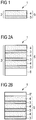
- the thickness of the first ALD layer 3 is according to the embodiment FIG. 1 at about 10 nm
- the second ALD layer 4 has a thickness of about 1 nm.
- the two ALD layers 3, 4 according to the embodiment of the FIG. 1 form a nanolaminate 5.
- a nanolaminate 5 alone may be capable of providing a sufficient barrier to atmospheric influences such as moisture or oxygen.
- a thin-film encapsulation 1 according to the present application is formed by a nanolaminate 5 in which the ALD layers 3, 4 repeat periodically.
- the thin-layer encapsulation 1 according to the exemplary embodiment of FIG. 2A has, for example, a nanolaminate 5, in which the ALD layers 3, 4 of the nanolaminate according to FIG. 1 repeat periodically three times.
- the ALD layers 3, 4 are each arranged in direct contact with each other, that is, they each form a common interface.
- the ALD layers 3, 4 of the nanolaminate 5 repeat FIG. 1 at least five times. This is not shown for reasons of clarity.
- a further layer 6 which is not applied by means of atomic layer deposition, but for example by thermal evaporation or plasma-assisted processes, such as sputtering or PECVD.
- the further layer 6 is in this case arranged in direct contact with the outermost first ALD layer 3 of the nanolaminate 5.
- the further layer 6 comprises silicon nitride or consists of silicon nitride and has a thickness of, for example, approximately 90 nm.
- silicon oxide silicon oxide, silicon oxynitride, indium tin oxide, indium zinc oxide, aluminum-doped zinc oxide, aluminum oxide and their mixtures and alloys are suitable for the further layer 6.
- the thin-layer encapsulation 1 according to the exemplary embodiment of FIG. 2B , which is not part of the invention, comprises a first ALD layer 3, which, as in the embodiment according to FIG. 2A Has alumina or consists of alumina. Furthermore, the thin-layer encapsulation 1 has a second ALD layer 4 which comprises titanium oxide or consists of titanium oxide. The first ALD layer 3 is applied in direct contact with the second ALD layer 4.
- the nanolaminate 5 according to the embodiment of the FIG. 2B which is not part of the invention is formed by a threefold periodic repetition of a first ALD layer 3 comprising alumina or consisting of alumina and a second ald layer 4 comprising titania or consisting of titania. Furthermore, it is also possible that the nanolaminate 5 is formed by a quadruple or about five times periodic repetition of such first and second ALD layers 3, 4.
- the thickness of the first ALD layer 3 and the second ALD layer 4 is preferably between one atomic layer and 10 nm.
- the thickness of the first ALD layer 3, which comprises aluminum oxide or consists of aluminum oxide is about 2 nm.
- the thickness of the second ALD layer 4, which comprises titanium oxide or consists of titanium oxide, is for example between about 7 nm and about 9 nm, the limits being included.
- the thin-layer encapsulation according to the embodiment of the FIG. 2B which is not part of the invention, intended to be applied to an optoelectronic component with the first ALD layer 3 comprising aluminum oxide or consisting of aluminum oxide, so that a second ALD layer 4 comprising titanium oxide or consisting of titanium oxide , an outer surface of the thin-film encapsulation 1 forms.
- the layer sequence 2 of the thin-layer encapsulation 1 it is also possible for the layer sequence 2 of the thin-layer encapsulation 1 to have a further ALD layer 6 'which likewise comprises titanium oxide or consists of titanium oxide and which forms the outer surface of the thin-layer encapsulation 1.
- Such a further ALD layer 6 ', which comprises titanium oxide or consists of titanium oxide has, for example, a thickness of approximately 8 nm.
- the thin-layer encapsulation 1 according to the exemplary embodiment of FIG. 3 differs from the thin-layer encapsulation 1 according to the FIG. 2A in that its layer sequence 2 comprises a second further layer 7.
- the second further layer 7 is applied to the side of the nanolaminate 5 facing away from the first further layer 6 in direct contact therewith.
- the second further layer 7 may comprise the same material as the first further layer 6 or also another material.
- the optoelectronic component according to the embodiment of the FIG. 4 has a substrate 8, to which an active zone 9 is applied.
- the active zone 9 is in this case suitable for receiving or emitting radiation.
- the active zone 9 of the device comprises, for example, an organic functional material.
- the active zone 9 may also comprise an inorganic active material.
- the optoelectronic component can be, for example, an organic light-emitting diode, an organic photovoltaic cell or a solar cell. Furthermore, the optoelectronic component can also comprise organic electronics, such as transistors, diodes or organic integrated circuits.
- a thin-film encapsulation 1 On the active zone 9 of the optoelectronic component is a thin-film encapsulation 1 according to the embodiment of FIG. 2A applied.
- the thin-film encapsulation 1 is applied to the active zone 9 in such a way that the further layer 6 faces the active zone 9 and the radiation generated or received in the active zone 9 passes through the thin-layer encapsulation 1.
- the optoelectronic device according to FIG. 4 could the optoelectronic device according to FIG. 4 also a thin-layer encapsulation 1 according to the embodiments of the FIGS. 1, 2B and 3 include.
- a thin-film encapsulation 1 which between the substrate 8 and the active zone 9 of the Component is arranged.
- the further layer 6 of the thin-layer encapsulation 1 faces the substrate 8.
- the active zone 9 is applied to the nanolaminate 5.
- the optoelectronic component according to the embodiment of the FIG. 6 has two thin-film encapsulations 1.
- the two Dünn fürverkapselept 1 are presently identical according to the embodiment of FIG. 2A educated. But they can also be designed differently from each other.
- the first thin-layer encapsulation 1 is as in the device according to the FIG. 5 between the substrate 8 and the active region 9, while the second thin-layer encapsulation 1 is arranged above the active region 9, as in the embodiment of FIGS FIG. 4 ,
Landscapes
- Chemical & Material Sciences (AREA)
- Physics & Mathematics (AREA)
- Inorganic Chemistry (AREA)
- Electromagnetism (AREA)
- Optics & Photonics (AREA)
- Engineering & Computer Science (AREA)
- Materials Engineering (AREA)
- Organic Chemistry (AREA)
- Manufacturing & Machinery (AREA)
- Metallurgy (AREA)
- Mechanical Engineering (AREA)
- Chemical Kinetics & Catalysis (AREA)
- General Chemical & Material Sciences (AREA)
- Electroluminescent Light Sources (AREA)
- Chemical Vapour Deposition (AREA)
- Physical Vapour Deposition (AREA)
Priority Applications (1)
| Application Number | Priority Date | Filing Date | Title |
|---|---|---|---|
| EP12161502A EP2472629A1 (de) | 2009-03-24 | 2010-03-22 | Dünnschichtverkapselung für ein optoelektronisches Bauelement, Verfahren zu dessen Herstellung und optoelektronisches Bauelement |
Applications Claiming Priority (3)
| Application Number | Priority Date | Filing Date | Title |
|---|---|---|---|
| DE102009014543 | 2009-03-24 | ||
| DE102009024411A DE102009024411A1 (de) | 2009-03-24 | 2009-06-09 | Dünnschichtverkapselung für ein optoelektronisches Bauelement, Verfahren zu dessen Herstellung und optoelektronisches Bauelement |
| PCT/EP2010/053717 WO2010108894A1 (de) | 2009-03-24 | 2010-03-22 | Dünnschichtverkapselung für ein optoelektronisches bauelement, verfahren zu dessen herstellung und optoelektronisches bauelement |
Related Child Applications (1)
| Application Number | Title | Priority Date | Filing Date |
|---|---|---|---|
| EP12161502A Division-Into EP2472629A1 (de) | 2009-03-24 | 2010-03-22 | Dünnschichtverkapselung für ein optoelektronisches Bauelement, Verfahren zu dessen Herstellung und optoelektronisches Bauelement |
Publications (2)
| Publication Number | Publication Date |
|---|---|
| EP2412040A1 EP2412040A1 (de) | 2012-02-01 |
| EP2412040B1 true EP2412040B1 (de) | 2018-07-18 |
Family
ID=42664172
Family Applications (2)
| Application Number | Title | Priority Date | Filing Date |
|---|---|---|---|
| EP10710030.7A Active EP2412040B1 (de) | 2009-03-24 | 2010-03-22 | Dünnschichtverkapselung für ein optoelektronisches bauelement, verfahren zu dessen herstellung und optoelektronisches bauelement |
| EP12161502A Withdrawn EP2472629A1 (de) | 2009-03-24 | 2010-03-22 | Dünnschichtverkapselung für ein optoelektronisches Bauelement, Verfahren zu dessen Herstellung und optoelektronisches Bauelement |
Family Applications After (1)
| Application Number | Title | Priority Date | Filing Date |
|---|---|---|---|
| EP12161502A Withdrawn EP2472629A1 (de) | 2009-03-24 | 2010-03-22 | Dünnschichtverkapselung für ein optoelektronisches Bauelement, Verfahren zu dessen Herstellung und optoelektronisches Bauelement |
Country Status (7)
| Country | Link |
|---|---|
| US (1) | US9444062B2 (enExample) |
| EP (2) | EP2412040B1 (enExample) |
| JP (1) | JP6073130B2 (enExample) |
| KR (1) | KR101722277B1 (enExample) |
| CN (1) | CN102362369B (enExample) |
| DE (1) | DE102009024411A1 (enExample) |
| WO (1) | WO2010108894A1 (enExample) |
Families Citing this family (62)
| Publication number | Priority date | Publication date | Assignee | Title |
|---|---|---|---|---|
| DE102009024411A1 (de) | 2009-03-24 | 2010-09-30 | Osram Opto Semiconductors Gmbh | Dünnschichtverkapselung für ein optoelektronisches Bauelement, Verfahren zu dessen Herstellung und optoelektronisches Bauelement |
| FR2949776B1 (fr) | 2009-09-10 | 2013-05-17 | Saint Gobain Performance Plast | Element en couches pour l'encapsulation d'un element sensible |
| FR2949775B1 (fr) | 2009-09-10 | 2013-08-09 | Saint Gobain Performance Plast | Substrat de protection pour dispositif collecteur ou emetteur de rayonnement |
| FR2973939A1 (fr) | 2011-04-08 | 2012-10-12 | Saint Gobain | Element en couches pour l’encapsulation d’un element sensible |
| FR2973940A1 (fr) * | 2011-04-08 | 2012-10-12 | Saint Gobain | Element en couches pour l’encapsulation d’un element sensible |
| DE102011079004A1 (de) | 2011-07-12 | 2013-01-17 | Osram Opto Semiconductors Gmbh | Organisches lichtemittierendes bauelement und verfahren zum herstellen eines organischen lichtemittierenden bauelements |
| DE102011079048B4 (de) | 2011-07-13 | 2025-09-11 | Pictiva Displays International Limited | Lichtemittierende bauelemente und verfahren zum herstellen eines lichtemittierenden bauelements |
| CN103718324B (zh) | 2011-07-14 | 2016-10-19 | 欧司朗Oled股份有限公司 | 用于光电子器件的封装结构和用于封装光电子器件的方法 |
| DE102011113428A1 (de) | 2011-09-14 | 2013-03-14 | Osram Opto Semiconductors Gmbh | Optoelektronisches Bauelement |
| DE102011084276B4 (de) | 2011-10-11 | 2019-10-10 | Osram Oled Gmbh | Verkapselung für ein organisches elektronisches bauelement, ein organisches elektronisches bauelement mit der verkapselung und ein verfahren zur herstellung eines organischen elektronischen bauelements mit der verkapselung |
| DE102012203212B4 (de) | 2012-03-01 | 2025-02-27 | Osram Oled Gmbh | Beschichtungsanlage und verfahren zur durchführung eines aufwachsprozesses |
| DE102012208142B4 (de) | 2012-05-15 | 2021-05-12 | Pictiva Displays International Limited | Organisches licht emittierendes bauelement und verfahren zur herstellung eines organischen licht emittierenden bauelements |
| DE102012211869A1 (de) | 2012-07-06 | 2014-01-09 | Osram Opto Semiconductors Gmbh | Organisches Licht emittierendes Bauelement |
| DE102012214216A1 (de) | 2012-08-09 | 2014-02-13 | Osram Opto Semiconductors Gmbh | Organisches Leuchtdiodenmodul und Verfahren zu dessen Herstellung |
| DE102012214325B4 (de) | 2012-08-10 | 2017-06-08 | Osram Oled Gmbh | Verfahren zum Herstellen eines optoelektronischen Bauelementes und Verfahren zum Strukturieren eines organischen, optoelektronischen Bauelementes |
| KR101970361B1 (ko) | 2012-08-20 | 2019-04-19 | 삼성디스플레이 주식회사 | 유기 발광 표시 장치 및 이의 제조방법 |
| CN102864417A (zh) * | 2012-08-22 | 2013-01-09 | 吉林大学 | 电子束蒸发结合原子层沉积钝化层实现有机器件封装的方法 |
| DE102012215708A1 (de) | 2012-09-05 | 2014-03-06 | Osram Opto Semiconductors Gmbh | Vorratsbehälter für eine beschichtungsanlage und beschichtungsanlage |
| DE102012221080A1 (de) * | 2012-11-19 | 2014-03-06 | Osram Opto Semiconductors Gmbh | Verfahren zur Herstellung einer Schicht auf einem Oberflächenbereich eines elektronischen Bauelements |
| EP2927346A4 (en) * | 2012-11-29 | 2016-07-20 | Lg Chemical Ltd | COATING METHOD FOR REDUCING DAMAGE TO A SHOCK LAYER |
| JP6036279B2 (ja) * | 2012-12-26 | 2016-11-30 | コニカミノルタ株式会社 | 有機エレクトロルミネッセンス素子製造方法 |
| CN106486601A (zh) | 2013-04-30 | 2017-03-08 | 成均馆大学校产学协力团 | 多层封装薄膜 |
| KR101465212B1 (ko) * | 2013-04-30 | 2014-11-25 | 성균관대학교산학협력단 | 초극유연성 봉지 박막 |
| DE102013105128A1 (de) | 2013-05-17 | 2014-11-20 | Osram Opto Semiconductors Gmbh | Optoelektronisches Bauelement |
| KR20150018964A (ko) | 2013-08-12 | 2015-02-25 | 삼성디스플레이 주식회사 | 유기전계발광 표시장치 및 그의 제조방법 |
| DE102013108871A1 (de) | 2013-08-16 | 2015-03-12 | Osram Opto Semiconductors Gmbh | Organisches Licht emittierendes Bauelement |
| DE102013109646B4 (de) | 2013-09-04 | 2021-12-02 | Pictiva Displays International Limited | Organisches optoelektronisches Bauelement |
| EP3016162B1 (en) * | 2013-09-30 | 2020-07-22 | LG Chem, Ltd. | Substrate for organic electronic devices and production method therefor |
| KR101928598B1 (ko) * | 2013-09-30 | 2018-12-12 | 주식회사 엘지화학 | 폴리이미드 필름 및 그 제조방법 |
| FR3020179B1 (fr) * | 2014-04-22 | 2017-10-06 | Saint Gobain | Electrode supportee transparente pour oled |
| DE102014106549B4 (de) | 2014-05-09 | 2023-10-19 | Pictiva Displays International Limited | Organisches Licht emittierendes Bauelement |
| DE102014108282A1 (de) | 2014-06-12 | 2015-12-17 | Osram Opto Semiconductors Gmbh | Optoelektronisches Halbleiterbauelement, Verfahren zur Herstellung eines optoelektronischen Halbleiterbauelements sowie Lichtquelle mit einem optoelektronischen Halbleiterbauelement |
| EP2960315A1 (de) | 2014-06-27 | 2015-12-30 | cynora GmbH | Organische Elektrolumineszenzvorrichtung |
| DE102014110969A1 (de) | 2014-08-01 | 2016-02-04 | Osram Oled Gmbh | Organisches Bauteil sowie Verfahren zur Herstellung eines organischen Bauteils |
| DE102014118354A1 (de) | 2014-09-12 | 2016-03-17 | Osram Oled Gmbh | Organisches Bauelement |
| KR102251715B1 (ko) | 2014-09-17 | 2021-05-12 | 시노라 게엠베하 | 이미터로서 사용하기 위한 유기 분자 |
| DE102014116141B4 (de) | 2014-11-05 | 2022-07-28 | OSRAM Opto Semiconductors Gesellschaft mit beschränkter Haftung | Verfahren zur Herstellung zumindest eines optoelektronischen Halbleiterchips, optoelektronischer Halbleiterchip sowie optoelektronisches Halbleiterbauelement |
| DE102014223507A1 (de) | 2014-11-18 | 2016-05-19 | Osram Oled Gmbh | Organisches Licht emittierendes Bauelement und Verfahren zur Herstellung eines organischen Licht emittierenden Bauelements |
| JP2016100315A (ja) * | 2014-11-26 | 2016-05-30 | パイオニア株式会社 | 発光装置 |
| JP2016103443A (ja) * | 2014-11-28 | 2016-06-02 | パイオニア株式会社 | 発光装置 |
| KR102382025B1 (ko) * | 2015-03-04 | 2022-04-04 | 삼성디스플레이 주식회사 | 표시 장치 |
| DE102015105766A1 (de) | 2015-04-15 | 2016-10-20 | Osram Oled Gmbh | Haltevorrichtung für eine organische Leuchtdiode und OLED-Modul |
| DE102015107471A1 (de) | 2015-05-12 | 2016-11-17 | Osram Oled Gmbh | Organisches Licht emittierendes Bauelement |
| US9847511B2 (en) * | 2015-05-14 | 2017-12-19 | Applied Materials, Inc. | Encapsulating film stacks for OLED applications |
| DE102015110241A1 (de) | 2015-06-25 | 2016-12-29 | Osram Oled Gmbh | Verfahren zur Steuerung eines organischen Licht emittierenden Bauelements, Licht emittierende Vorrichtung mit einem organischen Licht emittierenden Bauelement und Scheinwerfer mit einer Licht emittierenden Vorrichtung |
| DE102015118417A1 (de) | 2015-10-28 | 2017-05-04 | Osram Oled Gmbh | Optoelektronisches Bauelement und Verfahren zum Herstellen eines optoelektronischen Bauelements |
| CN105449123B (zh) * | 2015-11-18 | 2018-03-06 | 上海大学 | 水氧阻隔层的制备方法 |
| KR102228408B1 (ko) * | 2016-10-06 | 2021-03-17 | 주식회사 원익아이피에스 | 하드 마스크 제조방법 |
| KR102228412B1 (ko) * | 2016-11-03 | 2021-03-17 | 주식회사 원익아이피에스 | 하드 마스크 제조방법 |
| KR102268492B1 (ko) * | 2017-09-22 | 2021-06-25 | 주식회사 원익아이피에스 | 복합막 제조방법 |
| TWI661076B (zh) * | 2016-10-06 | 2019-06-01 | 南韓商圓益Ips股份有限公司 | 複合膜製造方法 |
| KR102517378B1 (ko) * | 2016-11-07 | 2023-04-04 | 더 리젠츠 오브 더 유니버시티 오브 콜로라도, 어 바디 코포레이트 | 테크니컬 세라믹의 개선된 성능 |
| JP6924023B2 (ja) * | 2016-12-16 | 2021-08-25 | パイオニア株式会社 | 発光装置 |
| JP6815901B2 (ja) * | 2017-03-06 | 2021-01-20 | 株式会社日本製鋼所 | 表示装置およびその製造方法 |
| CN108666438A (zh) * | 2017-04-01 | 2018-10-16 | 上海和辉光电有限公司 | 显示面板以及显示装置 |
| CN107819075A (zh) * | 2017-11-02 | 2018-03-20 | 长沙新材料产业研究院有限公司 | 一种在浮空器囊体上集成柔性钙钛矿太阳能电池的方法 |
| CN108598198A (zh) * | 2018-04-26 | 2018-09-28 | 上海空间电源研究所 | 一种耐原子氧柔性高透明导电封装材料 |
| JP2019195001A (ja) * | 2019-08-20 | 2019-11-07 | パイオニア株式会社 | 発光装置 |
| KR20220097462A (ko) * | 2019-11-07 | 2022-07-07 | 외를리콘 서피스 솔루션즈 아게, 페피콘 | 코팅의 제조 방법 |
| JP2020053411A (ja) * | 2019-12-26 | 2020-04-02 | パイオニア株式会社 | 発光装置 |
| US12016241B2 (en) | 2020-02-13 | 2024-06-18 | Samsung Electronics Co., Ltd. | Quantum dot device, method of manufacturing the same, and electronic device |
| KR102764010B1 (ko) | 2020-04-29 | 2025-02-05 | 삼성전자주식회사 | 센서 및 전자 장치 |
Citations (2)
| Publication number | Priority date | Publication date | Assignee | Title |
|---|---|---|---|---|
| US20060017383A1 (en) * | 2004-07-20 | 2006-01-26 | Denso Corporation | Color organic EL display and method for manufacturing the same |
| US20070295390A1 (en) * | 2006-05-05 | 2007-12-27 | Nanosolar, Inc. | Individually encapsulated solar cells and solar cell strings having a substantially inorganic protective layer |
Family Cites Families (35)
| Publication number | Priority date | Publication date | Assignee | Title |
|---|---|---|---|---|
| US4507393A (en) * | 1983-08-11 | 1985-03-26 | Schott Glass Technologies, Inc. | Highly prefractive, low dispersion optical glass suitable for multifocal corrective lenses |
| ATE266745T1 (de) | 1999-04-03 | 2004-05-15 | Leibniz Inst Fuer Festkoerper | Metallischer werkstoff auf nickelbasis und verfahren zu dessen herstellung |
| US7198832B2 (en) * | 1999-10-25 | 2007-04-03 | Vitex Systems, Inc. | Method for edge sealing barrier films |
| JP4556282B2 (ja) | 2000-03-31 | 2010-10-06 | 株式会社デンソー | 有機el素子およびその製造方法 |
| FI118014B (fi) | 2000-10-23 | 2007-05-31 | Asm Int | Menetelmä alumiinioksidiohutkalvojen valmistamiseksi matalissa lämpötiloissa |
| JP3687582B2 (ja) * | 2001-09-12 | 2005-08-24 | ウシオ電機株式会社 | 放電ランプ |
| JP3724454B2 (ja) * | 2002-05-31 | 2005-12-07 | 株式会社デンソー | 薄膜の形成方法 |
| DE10307095A1 (de) * | 2003-02-19 | 2004-09-02 | Merck Patent Gmbh | Aufdampfmaterial zur Herstellung hochbrechender optischer Schichten |
| JP4186688B2 (ja) | 2003-04-17 | 2008-11-26 | 三菱化学株式会社 | エレクトロルミネッセンス素子 |
| US7212485B2 (en) * | 2003-04-14 | 2007-05-01 | Hoya Corporation | Objective lens and method for manufacture thereof |
| US20070275181A1 (en) | 2003-05-16 | 2007-11-29 | Carcia Peter F | Barrier films for plastic substrates fabricated by atomic layer deposition |
| CN1657976A (zh) * | 2004-02-16 | 2005-08-24 | 柯尼卡美能达精密光学株式会社 | 光学元件和光接收装置 |
| US20050181535A1 (en) * | 2004-02-17 | 2005-08-18 | Yun Sun J. | Method of fabricating passivation layer for organic devices |
| WO2006014591A2 (en) * | 2004-07-08 | 2006-02-09 | Itn Energy Systems, Inc. | Permeation barriers for flexible electronics |
| US20060063015A1 (en) * | 2004-09-23 | 2006-03-23 | 3M Innovative Properties Company | Protected polymeric film |
| JP5464775B2 (ja) | 2004-11-19 | 2014-04-09 | エイエスエム インターナショナル エヌ.ヴェー. | 低温での金属酸化物膜の製造方法 |
| WO2006095632A1 (ja) | 2005-03-11 | 2006-09-14 | Mitsubishi Chemical Corporation | エレクトロルミネッセンス素子及び照明装置 |
| JP5066814B2 (ja) * | 2005-03-11 | 2012-11-07 | 三菱化学株式会社 | エレクトロルミネッセンス素子及び照明装置 |
| JP2007052100A (ja) * | 2005-08-16 | 2007-03-01 | Konica Minolta Opto Inc | 光学反射部材 |
| KR100792139B1 (ko) * | 2006-02-06 | 2008-01-04 | 주식회사 엘지화학 | 전자주입층으로서 무기절연층을 이용한 유기발광소자 및이의 제조 방법 |
| US20070295388A1 (en) * | 2006-05-05 | 2007-12-27 | Nanosolar, Inc. | Solar assembly with a multi-ply barrier layer and individually encapsulated solar cells or solar cell strings |
| US7781031B2 (en) * | 2006-12-06 | 2010-08-24 | General Electric Company | Barrier layer, composite article comprising the same, electroactive device, and method |
| US8174187B2 (en) * | 2007-01-15 | 2012-05-08 | Global Oled Technology Llc | Light-emitting device having improved light output |
| US8241713B2 (en) | 2007-02-21 | 2012-08-14 | 3M Innovative Properties Company | Moisture barrier coatings for organic light emitting diode devices |
| JP2008235760A (ja) * | 2007-03-23 | 2008-10-02 | Denso Corp | 絶縁膜の製造方法 |
| DE102007024152A1 (de) * | 2007-04-18 | 2008-10-23 | Osram Opto Semiconductors Gmbh | Organisches optoelektronisches Bauelement |
| US20090081356A1 (en) * | 2007-09-26 | 2009-03-26 | Fedorovskaya Elena A | Process for forming thin film encapsulation layers |
| US20090079328A1 (en) * | 2007-09-26 | 2009-03-26 | Fedorovskaya Elena A | Thin film encapsulation containing zinc oxide |
| TWI420722B (zh) | 2008-01-30 | 2013-12-21 | 歐斯朗奧托半導體股份有限公司 | 具有封裝單元之裝置 |
| DE102008019900A1 (de) | 2008-01-30 | 2009-08-06 | Osram Opto Semiconductors Gmbh | Verfahren zur Herstellung eines organischen elektronischen Bauelements und organisches elektronisches Bauelement |
| DE102008048472A1 (de) | 2008-09-23 | 2010-03-25 | Osram Opto Semiconductors Gmbh | Vorrichtung mit Verkapselungsanordnung |
| DE102008031405A1 (de) | 2008-07-02 | 2010-01-07 | Osram Opto Semiconductors Gmbh | Verfahren zur Herstellung eines organischen elektronischen Bauelements und organisches elektronisches Bauelement |
| US20090278454A1 (en) * | 2008-05-12 | 2009-11-12 | Fedorovskaya Elena A | Oled display encapsulated with a filter |
| KR101084267B1 (ko) | 2009-02-26 | 2011-11-16 | 삼성모바일디스플레이주식회사 | 유기 발광 표시 장치 및 그 제조 방법 |
| DE102009024411A1 (de) | 2009-03-24 | 2010-09-30 | Osram Opto Semiconductors Gmbh | Dünnschichtverkapselung für ein optoelektronisches Bauelement, Verfahren zu dessen Herstellung und optoelektronisches Bauelement |
-
2009
- 2009-06-09 DE DE102009024411A patent/DE102009024411A1/de not_active Withdrawn
-
2010
- 2010-03-22 KR KR1020117025037A patent/KR101722277B1/ko not_active Expired - Fee Related
- 2010-03-22 JP JP2012501272A patent/JP6073130B2/ja not_active Expired - Fee Related
- 2010-03-22 WO PCT/EP2010/053717 patent/WO2010108894A1/de not_active Ceased
- 2010-03-22 US US13/260,560 patent/US9444062B2/en active Active
- 2010-03-22 EP EP10710030.7A patent/EP2412040B1/de active Active
- 2010-03-22 EP EP12161502A patent/EP2472629A1/de not_active Withdrawn
- 2010-03-22 CN CN201080013287.1A patent/CN102362369B/zh active Active
Patent Citations (2)
| Publication number | Priority date | Publication date | Assignee | Title |
|---|---|---|---|---|
| US20060017383A1 (en) * | 2004-07-20 | 2006-01-26 | Denso Corporation | Color organic EL display and method for manufacturing the same |
| US20070295390A1 (en) * | 2006-05-05 | 2007-12-27 | Nanosolar, Inc. | Individually encapsulated solar cells and solar cell strings having a substantially inorganic protective layer |
Also Published As
| Publication number | Publication date |
|---|---|
| CN102362369A (zh) | 2012-02-22 |
| JP6073130B2 (ja) | 2017-02-01 |
| KR20120001778A (ko) | 2012-01-04 |
| JP2012521623A (ja) | 2012-09-13 |
| EP2472629A1 (de) | 2012-07-04 |
| WO2010108894A1 (de) | 2010-09-30 |
| KR101722277B1 (ko) | 2017-03-31 |
| US9444062B2 (en) | 2016-09-13 |
| DE102009024411A1 (de) | 2010-09-30 |
| CN102362369B (zh) | 2016-10-26 |
| US20120132953A1 (en) | 2012-05-31 |
| EP2412040A1 (de) | 2012-02-01 |
Similar Documents
| Publication | Publication Date | Title |
|---|---|---|
| EP2412040B1 (de) | Dünnschichtverkapselung für ein optoelektronisches bauelement, verfahren zu dessen herstellung und optoelektronisches bauelement | |
| DE102014107264B4 (de) | Mit einem hydrophoben organischen dünnfilm verkapselte organische lichtemittierende anzeigevorrichtung und herstellungsverfahren dafür | |
| DE102013106392B4 (de) | Verfahren zur Herstellung einer Entspiegelungsschicht | |
| DE102012208142B4 (de) | Organisches licht emittierendes bauelement und verfahren zur herstellung eines organischen licht emittierenden bauelements | |
| WO2017178233A1 (de) | Mehrschichtige verkapselung, verfahren zur verkapselung und optoelektronisches bauelement | |
| EP3262446A1 (de) | Reflektorelement und verfahren zu dessen herstellung | |
| EP2614536A1 (de) | Dünnschichtverkapselung, optoelektronischer halbleiterkörper mit einer dünnschichtverkapselung und verfahren zur herstellung einer dünnschichtverkapselung | |
| EP2675935A1 (de) | Verfahren zum herstellen eines dünnfilms aus blei-zirkonat-titanat | |
| DE102011005612A1 (de) | Organisches Optoelektronisches Bauelement und Verfahren zur Herstellung eines Optoelektronischen Bauelements | |
| DE102016100907B4 (de) | Verfahren zur Herstellung eines reflexionsmindernden Schichtsystems | |
| DE102016100914B4 (de) | Verfahren zur Herstellung einer porösen Brechzahlgradientenschicht | |
| WO2013007488A1 (de) | Organisches optoelektronisches bauteil und verfahren zu dessen herstellung | |
| EP1786945B1 (de) | Verfahren zur herstellung eines strahlungsabsorbierenden optischen elements | |
| WO2019145229A1 (de) | Optoelektronisches bauelement und verfahren zur herstellung eines optoelektronischen bauelements | |
| DE102020200053A1 (de) | Verkapselungssystem für ein optoelektronisches Bauelement mit mindestens einer ersten Verkapselung und einer zweiten Verkapselung, optoelektronisches Bauelement mit einem solchen Verkapselungssystem | |
| DE102014119538A1 (de) | Optoelektronische Baugruppe und Verfahren zum Herstellen einer optoelektronischen Baugruppe | |
| DE102022120892B3 (de) | Reflexionsminderndes Schichtsystem mit einer elektrisch leitfähigen Oberfläche und Verfahren zur Herstellung eines reflexionsmindernden Schichtsystems | |
| DE102006042327B4 (de) | Vorrichtung und Verfahren zur Ausbildung dünner Siliciumnitridschichten auf Oberflächen von kristallinen Silicium-Solarwafern | |
| DE102010006134B4 (de) | UV-absorbierendes Schichtsystem, Verfahren zu dessen Herstellung und Kunststoffsubstrat | |
| WO2017012746A1 (de) | Herstellungsverfahren für eine mikromechanische fensterstruktur und entsprechende mikromechanische fensterstruktur | |
| WO2015082687A1 (de) | Optoelektronisches bauelement und verfahren zur herstellung eines optoelektronischen bauelements | |
| WO2017029367A1 (de) | Verfahren zur herstellung eines optoelektronischen bauelements und optoelektronisches bauelement | |
| DE102006046126A1 (de) | Verfahren zur Herstellung eines beschichteten Gegenstands durch Sputtern eines keramischen Targets | |
| DE102019135574A1 (de) | Verfahren zum Herstellen einer heterogen strukturierten Beschichtung eines optoelektronischen Bauelements, sowie ein optoelektronisches Bauelement mit einer solchen Beschichtung | |
| WO2017178234A1 (de) | Verfahren zur herstellung eines organischen lichtemittierenden bauelements und organisches lichtemittierendes bauelement |
Legal Events
| Date | Code | Title | Description |
|---|---|---|---|
| PUAI | Public reference made under article 153(3) epc to a published international application that has entered the european phase |
Free format text: ORIGINAL CODE: 0009012 |
|
| 17P | Request for examination filed |
Effective date: 20110921 |
|
| AK | Designated contracting states |
Kind code of ref document: A1 Designated state(s): AT BE BG CH CY CZ DE DK EE ES FI FR GB GR HR HU IE IS IT LI LT LU LV MC MK MT NL NO PL PT RO SE SI SK SM TR |
|
| DAX | Request for extension of the european patent (deleted) | ||
| RAP1 | Party data changed (applicant data changed or rights of an application transferred) |
Owner name: OSRAM OLED GMBH |
|
| 17Q | First examination report despatched |
Effective date: 20150820 |
|
| STAA | Information on the status of an ep patent application or granted ep patent |
Free format text: STATUS: EXAMINATION IS IN PROGRESS |
|
| GRAP | Despatch of communication of intention to grant a patent |
Free format text: ORIGINAL CODE: EPIDOSNIGR1 |
|
| STAA | Information on the status of an ep patent application or granted ep patent |
Free format text: STATUS: GRANT OF PATENT IS INTENDED |
|
| INTG | Intention to grant announced |
Effective date: 20180326 |
|
| GRAS | Grant fee paid |
Free format text: ORIGINAL CODE: EPIDOSNIGR3 |
|
| GRAA | (expected) grant |
Free format text: ORIGINAL CODE: 0009210 |
|
| STAA | Information on the status of an ep patent application or granted ep patent |
Free format text: STATUS: THE PATENT HAS BEEN GRANTED |
|
| AK | Designated contracting states |
Kind code of ref document: B1 Designated state(s): AT BE BG CH CY CZ DE DK EE ES FI FR GB GR HR HU IE IS IT LI LT LU LV MC MK MT NL NO PL PT RO SE SI SK SM TR |
|
| REG | Reference to a national code |
Ref country code: GB Ref legal event code: FG4D Free format text: NOT ENGLISH |
|
| REG | Reference to a national code |
Ref country code: CH Ref legal event code: EP |
|
| REG | Reference to a national code |
Ref country code: IE Ref legal event code: FG4D Free format text: LANGUAGE OF EP DOCUMENT: GERMAN |
|
| REG | Reference to a national code |
Ref country code: AT Ref legal event code: REF Ref document number: 1020295 Country of ref document: AT Kind code of ref document: T Effective date: 20180815 |
|
| REG | Reference to a national code |
Ref country code: DE Ref legal event code: R096 Ref document number: 502010015168 Country of ref document: DE |
|
| REG | Reference to a national code |
Ref country code: NL Ref legal event code: MP Effective date: 20180718 |
|
| REG | Reference to a national code |
Ref country code: LT Ref legal event code: MG4D |
|
| PG25 | Lapsed in a contracting state [announced via postgrant information from national office to epo] |
Ref country code: NL Free format text: LAPSE BECAUSE OF FAILURE TO SUBMIT A TRANSLATION OF THE DESCRIPTION OR TO PAY THE FEE WITHIN THE PRESCRIBED TIME-LIMIT Effective date: 20180718 |
|
| PG25 | Lapsed in a contracting state [announced via postgrant information from national office to epo] |
Ref country code: NO Free format text: LAPSE BECAUSE OF FAILURE TO SUBMIT A TRANSLATION OF THE DESCRIPTION OR TO PAY THE FEE WITHIN THE PRESCRIBED TIME-LIMIT Effective date: 20181018 Ref country code: GR Free format text: LAPSE BECAUSE OF FAILURE TO SUBMIT A TRANSLATION OF THE DESCRIPTION OR TO PAY THE FEE WITHIN THE PRESCRIBED TIME-LIMIT Effective date: 20181019 Ref country code: IS Free format text: LAPSE BECAUSE OF FAILURE TO SUBMIT A TRANSLATION OF THE DESCRIPTION OR TO PAY THE FEE WITHIN THE PRESCRIBED TIME-LIMIT Effective date: 20181118 Ref country code: PL Free format text: LAPSE BECAUSE OF FAILURE TO SUBMIT A TRANSLATION OF THE DESCRIPTION OR TO PAY THE FEE WITHIN THE PRESCRIBED TIME-LIMIT Effective date: 20180718 Ref country code: SE Free format text: LAPSE BECAUSE OF FAILURE TO SUBMIT A TRANSLATION OF THE DESCRIPTION OR TO PAY THE FEE WITHIN THE PRESCRIBED TIME-LIMIT Effective date: 20180718 Ref country code: FI Free format text: LAPSE BECAUSE OF FAILURE TO SUBMIT A TRANSLATION OF THE DESCRIPTION OR TO PAY THE FEE WITHIN THE PRESCRIBED TIME-LIMIT Effective date: 20180718 Ref country code: LT Free format text: LAPSE BECAUSE OF FAILURE TO SUBMIT A TRANSLATION OF THE DESCRIPTION OR TO PAY THE FEE WITHIN THE PRESCRIBED TIME-LIMIT Effective date: 20180718 Ref country code: BG Free format text: LAPSE BECAUSE OF FAILURE TO SUBMIT A TRANSLATION OF THE DESCRIPTION OR TO PAY THE FEE WITHIN THE PRESCRIBED TIME-LIMIT Effective date: 20181018 |
|
| PG25 | Lapsed in a contracting state [announced via postgrant information from national office to epo] |
Ref country code: ES Free format text: LAPSE BECAUSE OF FAILURE TO SUBMIT A TRANSLATION OF THE DESCRIPTION OR TO PAY THE FEE WITHIN THE PRESCRIBED TIME-LIMIT Effective date: 20180718 Ref country code: LV Free format text: LAPSE BECAUSE OF FAILURE TO SUBMIT A TRANSLATION OF THE DESCRIPTION OR TO PAY THE FEE WITHIN THE PRESCRIBED TIME-LIMIT Effective date: 20180718 Ref country code: HR Free format text: LAPSE BECAUSE OF FAILURE TO SUBMIT A TRANSLATION OF THE DESCRIPTION OR TO PAY THE FEE WITHIN THE PRESCRIBED TIME-LIMIT Effective date: 20180718 |
|
| REG | Reference to a national code |
Ref country code: DE Ref legal event code: R097 Ref document number: 502010015168 Country of ref document: DE |
|
| PG25 | Lapsed in a contracting state [announced via postgrant information from national office to epo] |
Ref country code: EE Free format text: LAPSE BECAUSE OF FAILURE TO SUBMIT A TRANSLATION OF THE DESCRIPTION OR TO PAY THE FEE WITHIN THE PRESCRIBED TIME-LIMIT Effective date: 20180718 Ref country code: IT Free format text: LAPSE BECAUSE OF FAILURE TO SUBMIT A TRANSLATION OF THE DESCRIPTION OR TO PAY THE FEE WITHIN THE PRESCRIBED TIME-LIMIT Effective date: 20180718 Ref country code: CZ Free format text: LAPSE BECAUSE OF FAILURE TO SUBMIT A TRANSLATION OF THE DESCRIPTION OR TO PAY THE FEE WITHIN THE PRESCRIBED TIME-LIMIT Effective date: 20180718 Ref country code: RO Free format text: LAPSE BECAUSE OF FAILURE TO SUBMIT A TRANSLATION OF THE DESCRIPTION OR TO PAY THE FEE WITHIN THE PRESCRIBED TIME-LIMIT Effective date: 20180718 |
|
| PLBE | No opposition filed within time limit |
Free format text: ORIGINAL CODE: 0009261 |
|
| STAA | Information on the status of an ep patent application or granted ep patent |
Free format text: STATUS: NO OPPOSITION FILED WITHIN TIME LIMIT |
|
| PG25 | Lapsed in a contracting state [announced via postgrant information from national office to epo] |
Ref country code: SK Free format text: LAPSE BECAUSE OF FAILURE TO SUBMIT A TRANSLATION OF THE DESCRIPTION OR TO PAY THE FEE WITHIN THE PRESCRIBED TIME-LIMIT Effective date: 20180718 Ref country code: DK Free format text: LAPSE BECAUSE OF FAILURE TO SUBMIT A TRANSLATION OF THE DESCRIPTION OR TO PAY THE FEE WITHIN THE PRESCRIBED TIME-LIMIT Effective date: 20180718 Ref country code: SM Free format text: LAPSE BECAUSE OF FAILURE TO SUBMIT A TRANSLATION OF THE DESCRIPTION OR TO PAY THE FEE WITHIN THE PRESCRIBED TIME-LIMIT Effective date: 20180718 |
|
| 26N | No opposition filed |
Effective date: 20190423 |
|
| PG25 | Lapsed in a contracting state [announced via postgrant information from national office to epo] |
Ref country code: SI Free format text: LAPSE BECAUSE OF FAILURE TO SUBMIT A TRANSLATION OF THE DESCRIPTION OR TO PAY THE FEE WITHIN THE PRESCRIBED TIME-LIMIT Effective date: 20180718 |
|
| PG25 | Lapsed in a contracting state [announced via postgrant information from national office to epo] |
Ref country code: MC Free format text: LAPSE BECAUSE OF FAILURE TO SUBMIT A TRANSLATION OF THE DESCRIPTION OR TO PAY THE FEE WITHIN THE PRESCRIBED TIME-LIMIT Effective date: 20180718 |
|
| REG | Reference to a national code |
Ref country code: CH Ref legal event code: PL |
|
| PG25 | Lapsed in a contracting state [announced via postgrant information from national office to epo] |
Ref country code: LU Free format text: LAPSE BECAUSE OF NON-PAYMENT OF DUE FEES Effective date: 20190322 |
|
| REG | Reference to a national code |
Ref country code: BE Ref legal event code: MM Effective date: 20190331 |
|
| PG25 | Lapsed in a contracting state [announced via postgrant information from national office to epo] |
Ref country code: IE Free format text: LAPSE BECAUSE OF NON-PAYMENT OF DUE FEES Effective date: 20190322 Ref country code: LI Free format text: LAPSE BECAUSE OF NON-PAYMENT OF DUE FEES Effective date: 20190331 Ref country code: CH Free format text: LAPSE BECAUSE OF NON-PAYMENT OF DUE FEES Effective date: 20190331 |
|
| PG25 | Lapsed in a contracting state [announced via postgrant information from national office to epo] |
Ref country code: FR Free format text: LAPSE BECAUSE OF NON-PAYMENT OF DUE FEES Effective date: 20190331 Ref country code: BE Free format text: LAPSE BECAUSE OF NON-PAYMENT OF DUE FEES Effective date: 20190331 |
|
| PG25 | Lapsed in a contracting state [announced via postgrant information from national office to epo] |
Ref country code: TR Free format text: LAPSE BECAUSE OF FAILURE TO SUBMIT A TRANSLATION OF THE DESCRIPTION OR TO PAY THE FEE WITHIN THE PRESCRIBED TIME-LIMIT Effective date: 20180718 |
|
| PG25 | Lapsed in a contracting state [announced via postgrant information from national office to epo] |
Ref country code: PT Free format text: LAPSE BECAUSE OF FAILURE TO SUBMIT A TRANSLATION OF THE DESCRIPTION OR TO PAY THE FEE WITHIN THE PRESCRIBED TIME-LIMIT Effective date: 20181118 Ref country code: MT Free format text: LAPSE BECAUSE OF FAILURE TO SUBMIT A TRANSLATION OF THE DESCRIPTION OR TO PAY THE FEE WITHIN THE PRESCRIBED TIME-LIMIT Effective date: 20180718 |
|
| REG | Reference to a national code |
Ref country code: AT Ref legal event code: MM01 Ref document number: 1020295 Country of ref document: AT Kind code of ref document: T Effective date: 20190322 |
|
| REG | Reference to a national code |
Ref country code: DE Ref legal event code: R081 Ref document number: 502010015168 Country of ref document: DE Owner name: PICTIVA DISPLAYS INTERNATIONAL LIMITED, IE Free format text: FORMER OWNER: OSRAM OLED GMBH, 93049 REGENSBURG, DE Ref country code: DE Ref legal event code: R082 Ref document number: 502010015168 Country of ref document: DE Representative=s name: EPPING HERMANN FISCHER PATENTANWALTSGESELLSCHA, DE |
|
| PG25 | Lapsed in a contracting state [announced via postgrant information from national office to epo] |
Ref country code: AT Free format text: LAPSE BECAUSE OF NON-PAYMENT OF DUE FEES Effective date: 20190322 |
|
| PG25 | Lapsed in a contracting state [announced via postgrant information from national office to epo] |
Ref country code: CY Free format text: LAPSE BECAUSE OF FAILURE TO SUBMIT A TRANSLATION OF THE DESCRIPTION OR TO PAY THE FEE WITHIN THE PRESCRIBED TIME-LIMIT Effective date: 20180718 |
|
| PG25 | Lapsed in a contracting state [announced via postgrant information from national office to epo] |
Ref country code: HU Free format text: LAPSE BECAUSE OF FAILURE TO SUBMIT A TRANSLATION OF THE DESCRIPTION OR TO PAY THE FEE WITHIN THE PRESCRIBED TIME-LIMIT; INVALID AB INITIO Effective date: 20100322 |
|
| PG25 | Lapsed in a contracting state [announced via postgrant information from national office to epo] |
Ref country code: MK Free format text: LAPSE BECAUSE OF FAILURE TO SUBMIT A TRANSLATION OF THE DESCRIPTION OR TO PAY THE FEE WITHIN THE PRESCRIBED TIME-LIMIT Effective date: 20180718 |
|
| REG | Reference to a national code |
Ref country code: DE Ref legal event code: R079 Ref document number: 502010015168 Country of ref document: DE Free format text: PREVIOUS MAIN CLASS: H01L0051520000 Ipc: H10K0050800000 |
|
| PGFP | Annual fee paid to national office [announced via postgrant information from national office to epo] |
Ref country code: GB Payment date: 20230323 Year of fee payment: 14 |
|
| GBPC | Gb: european patent ceased through non-payment of renewal fee |
Effective date: 20240322 |
|
| PG25 | Lapsed in a contracting state [announced via postgrant information from national office to epo] |
Ref country code: GB Free format text: LAPSE BECAUSE OF NON-PAYMENT OF DUE FEES Effective date: 20240322 |
|
| PG25 | Lapsed in a contracting state [announced via postgrant information from national office to epo] |
Ref country code: GB Free format text: LAPSE BECAUSE OF NON-PAYMENT OF DUE FEES Effective date: 20240322 |
|
| PGFP | Annual fee paid to national office [announced via postgrant information from national office to epo] |
Ref country code: DE Payment date: 20250320 Year of fee payment: 16 |