EP2408006B1 - Verfahren zur Herstellung von 3D-Interconnectstrukturen mit Luftspalten und zugehöriges Bauelement - Google Patents
Verfahren zur Herstellung von 3D-Interconnectstrukturen mit Luftspalten und zugehöriges Bauelement Download PDFInfo
- Publication number
- EP2408006B1 EP2408006B1 EP11174114.6A EP11174114A EP2408006B1 EP 2408006 B1 EP2408006 B1 EP 2408006B1 EP 11174114 A EP11174114 A EP 11174114A EP 2408006 B1 EP2408006 B1 EP 2408006B1
- Authority
- EP
- European Patent Office
- Prior art keywords
- substrate
- trench
- tsv
- airgap
- openings
- Prior art date
- Legal status (The legal status is an assumption and is not a legal conclusion. Google has not performed a legal analysis and makes no representation as to the accuracy of the status listed.)
- Active
Links
Images






Classifications
-
- H—ELECTRICITY
- H10—SEMICONDUCTOR DEVICES; ELECTRIC SOLID-STATE DEVICES NOT OTHERWISE PROVIDED FOR
- H10W—GENERIC PACKAGES, INTERCONNECTIONS, CONNECTORS OR OTHER CONSTRUCTIONAL DETAILS OF DEVICES COVERED BY CLASS H10
- H10W20/00—Interconnections in chips, wafers or substrates
- H10W20/01—Manufacture or treatment
- H10W20/021—Manufacture or treatment of interconnections within wafers or substrates
- H10W20/023—Manufacture or treatment of interconnections within wafers or substrates the interconnections being through-semiconductor vias
-
- H—ELECTRICITY
- H10—SEMICONDUCTOR DEVICES; ELECTRIC SOLID-STATE DEVICES NOT OTHERWISE PROVIDED FOR
- H10W—GENERIC PACKAGES, INTERCONNECTIONS, CONNECTORS OR OTHER CONSTRUCTIONAL DETAILS OF DEVICES COVERED BY CLASS H10
- H10W20/00—Interconnections in chips, wafers or substrates
- H10W20/01—Manufacture or treatment
- H10W20/021—Manufacture or treatment of interconnections within wafers or substrates
- H10W20/023—Manufacture or treatment of interconnections within wafers or substrates the interconnections being through-semiconductor vias
- H10W20/0234—Manufacture or treatment of interconnections within wafers or substrates the interconnections being through-semiconductor vias comprising etching via holes that stop on pads or on electrodes
-
- H—ELECTRICITY
- H10—SEMICONDUCTOR DEVICES; ELECTRIC SOLID-STATE DEVICES NOT OTHERWISE PROVIDED FOR
- H10W—GENERIC PACKAGES, INTERCONNECTIONS, CONNECTORS OR OTHER CONSTRUCTIONAL DETAILS OF DEVICES COVERED BY CLASS H10
- H10W20/00—Interconnections in chips, wafers or substrates
- H10W20/01—Manufacture or treatment
- H10W20/021—Manufacture or treatment of interconnections within wafers or substrates
- H10W20/023—Manufacture or treatment of interconnections within wafers or substrates the interconnections being through-semiconductor vias
- H10W20/0242—Manufacture or treatment of interconnections within wafers or substrates the interconnections being through-semiconductor vias comprising etching via holes from the back sides of the chips, wafers or substrates
-
- H—ELECTRICITY
- H10—SEMICONDUCTOR DEVICES; ELECTRIC SOLID-STATE DEVICES NOT OTHERWISE PROVIDED FOR
- H10W—GENERIC PACKAGES, INTERCONNECTIONS, CONNECTORS OR OTHER CONSTRUCTIONAL DETAILS OF DEVICES COVERED BY CLASS H10
- H10W20/00—Interconnections in chips, wafers or substrates
- H10W20/20—Interconnections within wafers or substrates, e.g. through-silicon vias [TSV]
-
- H—ELECTRICITY
- H10—SEMICONDUCTOR DEVICES; ELECTRIC SOLID-STATE DEVICES NOT OTHERWISE PROVIDED FOR
- H10W—GENERIC PACKAGES, INTERCONNECTIONS, CONNECTORS OR OTHER CONSTRUCTIONAL DETAILS OF DEVICES COVERED BY CLASS H10
- H10W20/00—Interconnections in chips, wafers or substrates
- H10W20/20—Interconnections within wafers or substrates, e.g. through-silicon vias [TSV]
- H10W20/211—Through-semiconductor vias, e.g. TSVs
- H10W20/217—Through-semiconductor vias, e.g. TSVs comprising ring-shaped isolation structures outside of the via holes
-
- H—ELECTRICITY
- H10—SEMICONDUCTOR DEVICES; ELECTRIC SOLID-STATE DEVICES NOT OTHERWISE PROVIDED FOR
- H10W—GENERIC PACKAGES, INTERCONNECTIONS, CONNECTORS OR OTHER CONSTRUCTIONAL DETAILS OF DEVICES COVERED BY CLASS H10
- H10W20/00—Interconnections in chips, wafers or substrates
- H10W20/01—Manufacture or treatment
- H10W20/071—Manufacture or treatment of dielectric parts thereof
- H10W20/072—Manufacture or treatment of dielectric parts thereof of dielectric parts comprising air gaps
-
- H—ELECTRICITY
- H10—SEMICONDUCTOR DEVICES; ELECTRIC SOLID-STATE DEVICES NOT OTHERWISE PROVIDED FOR
- H10W—GENERIC PACKAGES, INTERCONNECTIONS, CONNECTORS OR OTHER CONSTRUCTIONAL DETAILS OF DEVICES COVERED BY CLASS H10
- H10W20/00—Interconnections in chips, wafers or substrates
- H10W20/40—Interconnections external to wafers or substrates, e.g. back-end-of-line [BEOL] metallisations or vias connecting to gate electrodes
- H10W20/45—Interconnections external to wafers or substrates, e.g. back-end-of-line [BEOL] metallisations or vias connecting to gate electrodes characterised by their insulating parts
- H10W20/46—Interconnections external to wafers or substrates, e.g. back-end-of-line [BEOL] metallisations or vias connecting to gate electrodes characterised by their insulating parts comprising air gaps
-
- H—ELECTRICITY
- H10—SEMICONDUCTOR DEVICES; ELECTRIC SOLID-STATE DEVICES NOT OTHERWISE PROVIDED FOR
- H10W—GENERIC PACKAGES, INTERCONNECTIONS, CONNECTORS OR OTHER CONSTRUCTIONAL DETAILS OF DEVICES COVERED BY CLASS H10
- H10W72/00—Interconnections or connectors in packages
- H10W72/20—Bump connectors, e.g. solder bumps or copper pillars; Dummy bumps; Thermal bumps
- H10W72/241—Dispositions, e.g. layouts
- H10W72/244—Dispositions, e.g. layouts relative to underlying supporting features, e.g. bond pads, RDLs or vias
-
- H—ELECTRICITY
- H10—SEMICONDUCTOR DEVICES; ELECTRIC SOLID-STATE DEVICES NOT OTHERWISE PROVIDED FOR
- H10W—GENERIC PACKAGES, INTERCONNECTIONS, CONNECTORS OR OTHER CONSTRUCTIONAL DETAILS OF DEVICES COVERED BY CLASS H10
- H10W72/00—Interconnections or connectors in packages
- H10W72/20—Bump connectors, e.g. solder bumps or copper pillars; Dummy bumps; Thermal bumps
- H10W72/251—Materials
- H10W72/252—Materials comprising solid metals or solid metalloids, e.g. PbSn, Ag or Cu
-
- H—ELECTRICITY
- H10—SEMICONDUCTOR DEVICES; ELECTRIC SOLID-STATE DEVICES NOT OTHERWISE PROVIDED FOR
- H10W—GENERIC PACKAGES, INTERCONNECTIONS, CONNECTORS OR OTHER CONSTRUCTIONAL DETAILS OF DEVICES COVERED BY CLASS H10
- H10W72/00—Interconnections or connectors in packages
- H10W72/20—Bump connectors, e.g. solder bumps or copper pillars; Dummy bumps; Thermal bumps
- H10W72/29—Bond pads specially adapted therefor
-
- H—ELECTRICITY
- H10—SEMICONDUCTOR DEVICES; ELECTRIC SOLID-STATE DEVICES NOT OTHERWISE PROVIDED FOR
- H10W—GENERIC PACKAGES, INTERCONNECTIONS, CONNECTORS OR OTHER CONSTRUCTIONAL DETAILS OF DEVICES COVERED BY CLASS H10
- H10W72/00—Interconnections or connectors in packages
- H10W72/90—Bond pads, in general
Definitions
- the invention relates to the field of forming interconnect structures such as Through Silicon Vias (TSV) to be used in the stacking of semiconductor devices. More particularly, the present invention relates to methods of forming airgaps whereby said airgaps are surrounding at least part of a TSV interconnect structure in order to reduce the capacitance of the interconnect structure. The invention further relates to devices thus obtained.
- TSV Through Silicon Vias
- a suitable 3-dimensional interconnect so called “3D-Through Silicon Via” also referred to as “3D-TSV”
- 3D-TSV 3-dimensional interconnect
- a ring structure is provided in a substrate wherein the ring structure is filled with a dielectric material and wherein the ring structure is surrounding an inner pillar structure made of conductive material which is functioning as the through silicon via interconnect structure.
- the dielectric material applied in the ring structure can be a spin-on or spray-on or Chemical Vapor Deposited (CVD) deposited polymer as well as a deposited/grown oxide or nitride.
- CVD Chemical Vapor Deposited
- US2009/189256 discloses a semiconductor substrate comprising a TSV surrounded by a ring trench, which may optionally comprise an air gap.
- DE10205026 discloses another semiconductor device comprising a TSV surrounded by an air-filled ring trench.
- JP2009272490 discloses yet another semiconductor substrate with a TSV surrounded by a sealed air gap.
- the 3D-TSV interconnects of the present invention are also referred to as ultra-low capacitance TSV interconnects
- the present invention solves the problem of high capacitance by forming airgaps during the processing of said 3D-TSV, whereby said airgaps are at least partly surrounding said 3D-TSV, preferably said airgaps are formed in a trench-like structure, more preferably a trench-like ring structure, which is surrounding said 3D-TSV interconnect.
- Said 3D-TSV interconnect is preferably a conductive pillar, more preferably a conductive pillar comprising a metal such as copper or nickel or tungten.
- the metal is preferably deposited using electrochemical deposition (ECD) techniques. Alternatively the metal may be deposited using Chemical Vapor deposition (CVD).
- ECD electrochemical deposition
- CVD Chemical Vapor deposition
- the present invention relates to a semiconductor device and a method for making said device, the semiconductor device comprising at least one 3D-TSV interconnect and a surrounding trench-like structure, more preferably a trench-like ring structure (also referred to as "donut" structure) which comprises at least one airgap.
- Said 3D-TSV interconnect is preferably a pillar made of conductive material and being connected to the interconnect structures of for example another semiconductor substrate or another semiconductor device and/or another level of interconnect structures within the same semiconductor device.
- a 3D stacked semiconductor device can be obtained whereby the individual semiconductor devices (wafers, dies) are stacked and interconnected to each other in a vertical position by means of 3D-TSV interconnects having ultra-low capacitances such that these devices are very suitable for applications in the field of memory stacking of large numbers of parallel memory die (capacitance multiplied by number of die in stack), high speed digital and high frequency rf interconnects, such as rf-transceivers in mobile applications or high speed digital transceivers in telecommunication and high performance computation applications.
- a substrate preferably a semiconductor substrate comprising semiconductor active devices
- which comprises at least an interconnect structure which is surrounded by a spacer material, which is in turn surrounded by a trench-like structure with an airgap.
- the air gap is created by sealing a plurality of openings in a mask layer over the trench-like structure.
- Said interconnect structure is preferably a 3D-TSV in the form of a conductive inner pillar.
- Said surrounding trench-like structure is preferably a trench-like ring structure.
- the ring structure may be any closed loop structure such as for example a circular loop, also referred to as circular ring, a polygonal closed loop, also referred to as polygonal ring, a square loop, also referred to as square ring.
- the air gap may itself have a ring-like shape for surrounding the interconnect structure.
- the air gap may have a width parallel to a major surface of the substrate, in case of a ring-structure this may be the width, that is substantially smaller than the height of the air gap in a direction perpendicular to a major surface or the substrate.
- an additional surrounding spacer structure is situated in between the conductive inner pillar and the surrounding airgap structure.
- Said additional surrounding structure is preferably made of (remaining) substrate material.
- said additional surrounding structure has preferably a width Ws, which is preferably larger than 100 nm, Ws may be 0.5 ⁇ m, 1 ⁇ m, 1.5 ⁇ m, 2 ⁇ m, 2.5 ⁇ m, 3 ⁇ m, 4 ⁇ m, 5 ⁇ m or 10 ⁇ m.
- the thickness of this material has to be such that its strength is sufficient to support the thermomechanical forces resulting from the stresses in the inner TSV metallisation during thermal excursions.
- the circumferential or "hoop"-stress is a function of the TSV conductive inner pillar size and the width of the surrounding ring of material. This requirement may result in a minimum thickness of the ring surrounding the TSV conductive inner pillar of 2 to 5 ⁇ m in the case of Cu TSV in a Si substrate, depending on the via diameter used.
- said surrounding trench-like airgap structure has a width Wg in the range of 0.5 ⁇ m up to 5 ⁇ m, more preferably below 2 ⁇ m and is such that airgap pinch-off conditions are good, preferably optimal.
- the sidewalls of the trench structure may be fully or partially covered by the material used to pinch-off the airgap.
- the thickness of this layer on the sidewalls of the trench structure has to be at some positions in the trench less than halve the trench width to allow for an airgap to be formed in the trench.
- said sealing which pinches off the airgap is made of an insulating dielectric material such as an oxide, nitride, carbide, polymer of a combination of these materials.
- said conductive inner pillar structure is made of a material selected from copper (Cu), Nickel (Ni), tungsten (W) or any other metals used in the field.
- This metal may be deposited using electrochemical deposition (ECD) techniques or alternatively Chemical Vapor deposition (CVD).
- the conductive material can also be an alloy, an implanted semiconductor, conductive silicon, conducting polymers, carbon nanotubes.
- a metal paste consisting of metallic particles and organic binders, e.g. Ag paste, can be applied.
- Carbon nano tubes (CNT) and combination of CNT and Cu can be applied. Also combinations of above mentioned materials can be used.
- the step of depositing a conductive material allows to create an electrical interconnect with an external contact. This step can comprise various sub-steps. Extra layers underlying the conductive material or intermediate layers can be used. This can be for example improve the filling of the holes, adhesion of the conductive material, reduce the stress, prevent inter-diffusion of materials ...
- the inner pillar structure is completely made of conductive material, e.g. metal, so as to form a conductive pillar, e.g. metal pillar.
- said inner pillar structure further comprises a barrier layer, to prevent diffusion of metals from the inner pillar structure into the spacer region Ws, and/or a seed layer which is deposited before filling the inner pillar with conductive material e.g. by electroplating. Said seed layer required when filling the pillar by electro-chemical depostion (electroplating) and should cover the whole surface of the side walls and bottom wall of the inner pillar structure (being conformal, continuous).
- Said barrier layer is preferably made of a material selected from Ta, Ti, TaN, TiN, TiW, RuTa and combinations thereof and is deposited by state of the art deposition techniques such as PVD and CVD and combinations thereof and said seed layer is preferably made of a material selected from Cu, Ni, Co, W, Mn and may be applied for instance by Chemical Vapor Deposition (CVD), Physical Vapor Deposition (sputtering) (PVD), Atomic Layer Deposition (ALD), Electro Chemical Deposition (ECD), as well as by any other method known in the art.
- CVD Chemical Vapor Deposition
- PVD Physical Vapor Deposition
- ALD Atomic Layer Deposition
- ECD Electro Chemical Deposition
- electrical interconnect structure conductive pillar
- parallel TSV are formed within the same trench-like (ring) structure.
- a method for the fabrication of at least one electrical interconnect in a substrate starts with the step of providing a substrate (which may be thinned beforehand) made of substrate material and having a first main surface and then producing at least one hollow structure, preferably a trench-like structure, more preferably a trench-like ring structure in said first main surface of the substrate whereby the at least one hollow structure is surrounding an inner pillar structure of substrate material.
- the trench-like structure is created by depositing a mask layer having openings and etching through the openings using an alternating isotropic etching-passivation process until the desired depth of the trench-like structure is reached.
- a dielectric liner is deposited which pinches off the openings at the surface of the substrate such that an airgap is created in the center of said structure. In some embodiments, in this way an airgap having a ring-like shape may be formed.
- a hole is created in the inner pillar thereby creating a Through Silicon Via (TSV) hole having a bottom surface and an additional surrounding structure made of material, e.g. (remaining) substrate material, between the TSV hole and the trench-like structure with airgap.
- TSV Through Silicon Via
- Said TSV hole is then at least partly filled with a conductive material thereby creating an electrical interconnect structure suitable for forming an electrical path from the bottom surface of the hole up until the surface of the substrate.
- the step of creating a (TSV) hole is preferably performed using reactive ion etching, i.e. a pulsed etching technique comprising alternating steps of isotropic etching and passivation (such as for example the Bosch process).
- Said mask layer may be an oxide or nitride layer and is having openings with a width W mg and a spacing W mb at the locations where the trench-like (ring) structure and airgap are to be defined.
- the spacing W mb is maximum 2 times the undercut (scallop) produced during the DRIE process, preferably less.
- Said undercut depends on the W mg and the DRIE recipe selected. Typically the larger the W mg and the higher the etch rate, the higher the undercut will be.
- the hollow trench-like (ring) structure is created by etching through the openings of the mask layer using a pulsed etching technique comprising alternating steps of isotropic etching and passivation and wherein said steps are repeated (also referred to as "Bosch cycles") until the desired depth of the hollow ring structure is reached.
- Said alternating etching - passivation process is preferably using an SF 6 based plasma etching step alternated with a C 4 F 8 based plasma passivation step, optionally further comprising oxygen and/or inert gases in either or both steps. This process is characterised by an undercut of the mask layer and so-called scalloping of the sidewalls.
- This undercut should be such that it is larger than halve of the size of the spacing W mb of the openings in the masking layers. This will result in a complete removal of substrate material below the closely spaced openings in the masking layers. Repeating the process over multiple cycles will result in a progressive realisation of the trench, a process which is finalized when reaching the opposite site of the substrate material and the interconnect layers of the active devices. At this point, the masking layer with holes W mg and spacing W mb is a porous membrane across the trench structure.
- a dielectric layer is deposited to pinch of the holes in the membrane masking the etched trench.
- the deposited dielectric liner has preferably a minimal lateral thickness which is larger than the half width of the openings W mg in the membrane of the ring structure to ensure a proper sealing of the air gap in the trench sturcute.
- the TSV interconnect is formed in a way identical to the first aspect of the invention.
- the step of at least partly filling the TSV hole with a conductive material is performed.
- Said conductive material may be a metal such as Copper (Cu), Nickel (Ni), tungsten (W) or any other metals and/or alloy of metals using electrochemical deposition (ECD) techniques or alternatively Chemical Vapor deposition (CVD).)
- alternative conductive materials may be used such as an implanted semiconductor, conductive silicon, conducting polymers, carbon nanotubes.
- a metal paste consisting of metallic particles and organic binders, e.g. Ag paste, can be applied.
- Carbon nano tubes (CNT) and combination of CNT and Cu can be applied.
- Said TSV interconnect structure may then be further provided with a solder ball or bump. Thinning of the substrate (preferably down to 50 ⁇ m-100 ⁇ m) may also take place before the creation of TSV interconnects.
- a surrounding trench-like structure or a “structure surrounding the TSV” this may refer to a structure with any geometrical shape having a specific width W g and W s that is surrounding the actual final conductive part of the TSV. Examples are a circular ring, polygonal rings or square rings as illustrated in FIG. 5 and 6 .
- the surrounding structure is a ring structure surrounding the TSV this is often referred to in the state of the art as the "donut-approach”.
- the surrounding trench-like structure is separated from the TSV by remaining substrate (e.g. Si) material having at least a critical width W s , which is preferably larger than 100 nm, said remaining substrate structure is also referred to in this disclosure as an additional surrounding structure.
- a pulsed etching refers to a process in which an etching step is alternated with a deposition step and this is repeated to achieve nearly vertical structures. It is also referred to as the "The Bosch process".
- the plasma contains some ions, which attack the wafer from a nearly vertical direction.
- this pulsed etching preferably uses sulfur hexafluoride source gas [SF 6 ], while for the deposition of a chemically inert passivation layer, preferably a [C 4 F 8 ] source gas (optionally further including oxygen and/or inert gases) is used and each pulsed phase preferably lasts for several seconds.
- the passivation layer protects the entire substrate from further chemical attack and prevents further (lateral) etching.
- the directional ions that bombard the substrate attack the passivation layer at the bottom of the trench (but not along the sides).
- the etch/deposition steps are repeated many times over resulting in a large number of very small isotropic etch steps taking place only at the bottom of the etched pits.
- 100-1000 etch/deposit steps are needed.
- the cycle time can be adjusted: short cycles yield smoother walls, and long cycles yield a higher etch rate.
- Embodiments of the present invention relate to electrical interconnects having ultra-low capacitance, more preferably to through-hole or Through Silicon Via (TSV) interconnects and methods for producing said electrical through-hole interconnects.
- Said interconnects are preferably used for making 3D stacked semiconductor wafers and chips, e.g. Si wafers and chips, and for packaging applications of e.g. MEMS devices.
- the present invention is related to an electrical interconnect structure with good capacitance, more particular to an ultra-low capacitance (preferably lower than 50 fF) 3D-TSV interconnect structure.
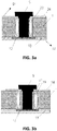
- FIG. 3 illustrates such an interconnect structure in the form of a conductive inner pillar structure with a surrounding trench-like structure e.g. in the form of a ring structure and wherein said trench-like structure is comprising an airgap and a sealing which pinches off said air gap.
- the air gap also may have a ring-like shape, such that the air gap also may be surrounding, the conductive inner pillar structure.
- the air gap may have a height in a direction perpendicular to a major or main surface of the substrate that is substantially higher than a thickness of the air gap in a direction parallel to a major or main surface of the substrate.
- FIG. 1A and 1B illustrate a semiconductor substrate 1 having state of the art 3D-TSV interconnects 5 wherein said 3D-TSV (5) comprises a conductive pillar acting as a TSV interconnect and a surrounding ring structure filled with a polymer or dielectric material (3).
- a process flow according to this state of the art 3D-TSV structure is illustrated in FIG. 2 .
- the method is based on producing a ring-structure 2a e.g. a ring-trench in the substrate (1) at the side of the surface (S1). This is done by using a photoresist layer on the first main surface (S1) in which a ring-like trench is defined, e.g. by using state of the art lithography techniques on the first main surface (S1).
- the ring-structure (2a) is fabricated in the substrate (1) by removing substrate material, e.g. by etching a circular trench in the substrate (1) e.g. Si substrate etch, thus producing an inner pillar structure (4) of substrate material.
- the ring-structure (2a) is then filled with a dielectric material (3), preferably a fluid, hereby also providing a layer of dielectric material (3) on the surface (S1) of the substrate.
- the inner pillar structure is then replaced with a conductive material (5).
- the TSV capacitance of this state of the art approach is simulated to be ⁇ 30fF which is not low enough for certain applications.
- FIG. 3A-3B illustrates a substrate comprising an electrical interconnect structure.
- the interconnect structure comprises a conductive inner pillar structure (5) surrounded by a trench-like structure such as a ring structure (R1) wherein said structure (R1) comprises at least one airgap (20) and a sealing material (24).
- the airgap also may have a ring-like shape so as to surround the conductive inner pillar structure.
- Said interconnect structure (5) may be a Through Silicon Via (TSV) having a high aspect ratio (ratio of the depth of TSV to the width of the TSV in the substrate), preferably said aspect ratio is 0.5, 1, 2, 5, 8, 10 or 20, more preferably said aspect ratio is in the range of 5 up to 10.
- the substrate thickness and hence TSV depth in the substrate is preferably 150 ⁇ m, 300 ⁇ m, 500 ⁇ m,725 ⁇ m and any value in between these values. More preferably the depth in the substrate is 20 ⁇ m up to 100 ⁇ m, most preferably a depth of around 50 ⁇ m.
- the conductive pillar of the TSV is preferably having a width of 1 ⁇ m diameter up to 100 ⁇ m in the range of 5 ⁇ m-25 ⁇ m, more preferably around 10 ⁇ m.
- the width of the TSV interconnect comprising the trench-like structure and the conductive pillar is 3 ⁇ m, 5 ⁇ m, 10 ⁇ m, 35 ⁇ m, 50 ⁇ m, 100 ⁇ m, 150 ⁇ m or any value in between.
- Said trench-like structure (R1) surrounding said interconnect structure (5) is comprising an airgap (20) and a sealing material (24) which pinches off the airgap (20).
- Said sealing material is preferably provided by depositing a liner (24) made of sealing material.
- the sealing material is preferably provided by depositing a liner (24) made of sealing material, more preferably a liner made of a dielectric material such as an oxide or nitride or alternatively a polymer.
- Said liner (24) is preferably deposited using a deposition technique selected from PE-CVD or PE-ALD , more preferably low temperature PE-CVD at temperatures typically ⁇ 200°C. In case the liner is a polymer, it may be deposited using spin coating or lamination.
- deposition of a liner (24) having a thickness onto the substrate surface of more than 1 ⁇ m is sufficient to achieve airgap pinch-off in the trench-like structure. For example depositing around 4.5 ⁇ m liner (e.g. oxide) thickness onto the substrate surface is sufficient to reach pinch-off on 2.5 ⁇ m wide trenches.
- the thickness of the liner (24) at the bottom of the trench after pinch-off is then typically in the range of 300nm-400nm.
- the average width of the trench-like structure (ring) structure (R1) is larger than 0.5 ⁇ m.
- the average width of the trench-like (ring) structure (R1) is smaller than 20 ⁇ m, or smaller than 10 ⁇ m, or smaller than 7 ⁇ m, or smaller than 6 ⁇ m or below 5 ⁇ m or below 4 ⁇ m, or can vary between 20 ⁇ m and 0.5 ⁇ m, between 10 ⁇ m and 0.5 ⁇ m, between 15 ⁇ m and 2 ⁇ m or between 10 ⁇ m and 3 ⁇ m or between 7 ⁇ m and 5 ⁇ m.
- the trench-like structure (R1) is preferably a ring structure but alternative geometrical surrounding structures as shown in FIG. 5 and FIG.6 are possible.
- the trench-like structure (R1) is having sloped sidewalls (such that the upper width Wg 1 is larger than the lower width Wg 2 of the trench) in order to position the airgap (20) pinch-off by the liner material deeper in the trench and to avoid pinch-off at a level above the substrate surface (S1).
- a trench-like structure having sloped sidewalls requires less liner material (smaller thickness Wd y' ) to be deposited onto the surface of the substrate to achieve airgap pinch-off.
- a trench-like structure having sloped sidewalls as illustrated in FIG. 8B has the additional advantage that pinch off is below the substrate surface and the airgap will not reopen during chemical Mechanical Polishing (CMP) steps performed later on to remove liner material from the field area.
- CMP chemical Mechanical Polishing
- the conductive pillar (5) is a Through Silicon Via (TSV) and is at least comprising a material selected from the group consisting of conductive silicon, Cu, Al, and W and optionally comprises a seed layer (not illustrated in the drawings). Furthermore said conductive pillar may comprise a barrier material (layer) at the outer sidewalls of the conductive pillar (not illustrated in the drawings). Said barrier material is preferably selected from materials such as Ta, Ti, TaN, TiN, RuTa, TiW, deposited by state of the art deposition techniques such as PVD and CVD and combinations thereof.
- TSV Through Silicon Via
- Said additional surrounding structure (21) is giving mechanical support to the conductive pillar (5) and avoids damage to the airgap (20) during the patterning (etching) of the hole (23) to create the conductive pillar (5) in the substrate (1).
- Said additional surrounding structure (21) is preferably made of substrate material and has preferably a width Ws, which is preferably larger than 100 nm.
- a minimum thickness of the additional surrounding structure is in range of 2 to 5 ⁇ m in the case of Cu TSV in a Si substrate and is further depending on the via diameter used.
- the trench-like structure (R1) is achieved by first depositing a layer (41) onto the substrate (40) and create openings (43) in said layer such that a hollow trench-like structure (R1) can be achieved by removing substrate material through said openings (43) using a pulsed etching technique comprising alternating steps of isotropic etching and passivation through said openings.
- the layer (41) in which openings (43) are created is preferably a RIE mask layer deposition such as an oxide or nitride comprising layer.
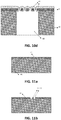
- FIG. 12 and 13 illustrates the radial distribution of the openings in order to create a hollow trench-like ring structure using the pulsed etching technique.
- FIGS. 9A and 9B illustrate the subsequent sealing or closure of the openings (43) in the deposited (mask) layer (41) in order to create an airgap (pinch-off).
- Said openings (43) are closed after creation of the hollow trench-like (ring) structure (R1) by depositing an additional (sealing) layer (44) e.g. an oxide.
- the openings (43) in the deposited layer (41) have a predefined width W mg and the spacing W mb between the openings (43) is maximum 2 times the undercut (scallop) produced during the DRIE process, preferably less.
- Said undercut depends on the W mg and the DRIE recipe selected. Typically the larger the openings (W mg ) and the higher the etch rate, the higher the undercut will be.
- the present invention is related to a method for fabrication an electrical interconnect structure, more specifically a 3D-TSV interconnect structure with improved (ultra-low) capacitance.
- FIG. 7A-7F A general overview of method steps of a method for the fabrication of the electrical interconnects in a substrate (1) are illustrated in FIG. 7A-7F . These drawings are cross-sections through the substrate (1) in a direction perpendicular to a main surface (S1) of the substrate (1).
- a process flow preferably starts with the step of providing a substrate (1) made of substrate material, said substrate (1) having a first main surface (S1).
- Said first main surface is preferably the backside of a semiconductor wafer comprising active devices (chips) in the front (opposite) surface of the substrate.
- the substrate (1) can be a wafer or a processed wafer. It can contain microelectronics components, possibly bonded to a wafer.
- the substrate (1) is a semiconductor substrate.
- the substrate (1) may comprise silicon or conductive silicon (for example realized by implantation), and in particular embodiments may be a silicon substrate or a conductive silicon substrate.
- the substrate (1) may comprise electronic or MEMS devices.
- the substrate (1) is a semiconductor wafer or die comprising a back-end-of-line (BEOL) and a front-end-of-line (FEOL), wherein the first main surface (S1) is the backside of the wafer or die, i.e. the side which is most remote from the BEOL (13) as illustrated in FIG. 3A-3B .
- the substrate thickness (e.g. after thinning the substrate beforehand) may be between 10 ⁇ m and 500 ⁇ m, for example between 20 ⁇ m and 300 ⁇ m, e.g. between 20 ⁇ m and 100 ⁇ m. In particular embodiments, the substrate thickness may be about 50 ⁇ m.
- a hollow trench-like structure (R1) is provided, preferably a trench like structure in the form of a ring (R1), in the substrate (1) at the side of the first main surface (S1).
- This can be done in one set of examples by providing a photoresist layer and/or a mask layer (2) on the first main surface (S1) in which a trench-like (ring) structure (R1) can be defined, e.g. by using state of the art lithography techniques on the first main surface (S1).
- the trench-like (ring) structure (R1) is fabricated in the substrate (1) by removing substrate material, e.g. by etching a trench, preferably a circular-like trench, in the substrate (1) e.g.
- the hollow trench-like structure (R1) is preferably produced in the substrate (1) from the first main surface (S1) towards a second main surface (S2) opposite the first main surface (S1), the hollow trench-like (ring) structure (R1) surrounding an inner pillar structure (22) of substrate material as illustrated in FIG. 7C .
- Said hollow trench like structure (R1) does advantageously not extend down to the second surface (S2), such that the structure (R1) has a bottom surface as illustrated in FIG. 3A and 4A .
- a process step for closing a through substrate trench like structure at the bottom also may be provided.
- the hollow trench like structure (R1) may be produced by etching the substrate (1), e.g.
- the hollow trench-like structure (R1) has a constant width.
- the hollow trench-like structure (R1) is defined in the plane of the first main surface (S1) by 2 concentrically circles and is further defined in the direction orthogonal to the first main surface (S1) by an inner and an outer sidewall (32, 33) corresponding to the trench-like structures (see FIG. 5 and 6 ).
- the width of trench-like structures (R1) is defined by the average distance between the 2 sidewalls (32, 33).
- the width W g of the hollow trench-like (ring) structure (R1) is predetermined such that the dimensions are optimal for the subsequent pinch-off conditions for airgap creation.
- Said surrounding trench-like structure preferably has a width Wg in the range of 0.5 ⁇ m up to 5 ⁇ m, more preferably below 2 ⁇ m.
- a liner (24) and preferably a dielectric liner (24), is deposited onto the surface (S1) of the substrate (1).
- Said liner deposition is such that it pinches off the hollow trench-like (ring) structure (R1) at least at the surface (S1) of the substrate (1) and preferably at a level below the surface (S1) of the substrate (1) such that an airgap (20) is created in the center of the (ring) structure (R1) thereby forming e.g. an airgap ring.
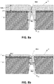
- FIG. 8A illustrates more in detail the deposition of the dielectric liner and resulting pinch-off.
- the dielectric liner material should at least partially cover the upper part of the sidewall of the hollow trench like (ring) structure (R1).
- the deposited dielectric liner (24) should have a minimal thickness W dx larger than halve the maximum width of the airgap trench W g resulting in W dx ⁇ W g /2.
- the formation of the pinch-off in order to create an air-gap typically requires a vertical deposition thickness W dy of the dielectric material in excess of the airgap width W g . For wider airgaps, e.g. several ⁇ m wide, this results in a relatively thick verticle dielectric liner thickness W dy .
- the sidewalls of the trench structure may be fully or partially covered by the material used to pinch-off the airgap.
- the pinch-off point may be further optimized by providing a trench-like structure (R1) having sloped sidewalls as illustrated in FIG. 8B in order to position the airgap pinch-off by the liner material deeper in the trench and to avoid pinch-off at a level above the substrate surface (S1) thereby requiring a smaller lateral dielectric liner thickness W dy' .
- a 6 ⁇ m dielectric (e.g. oxide) deposition can pinch-off a trench-like structure with straight sidewalls having W g of around 5 ⁇ m.
- a hole (23) is created in the inner pillar (22) thereby creating a Through Silicon Via (TSV) hole (23) having a bottom and sidewalls.
- Said TSV hole (23) is then at least partly filled with a conductive material thereby creating an electrical interconnect structure (5) suitable for forming an electrical path from the bottom surface of the hole up until the surface of the substrate (1) as illustrated in FIG. 7F .
- the dielectric liner material (24) can be patterned so as to free at least the location of the substrate pillar structure (22), removing, e.g. etching away, the substrate pillar structure (22), e.g. silicon substrate or silicon substrate further comprising ILD layer, thus leaving a pillar vacancy (23).
- the width W1 (diameter) of the TSV hole (23) is such that there is still substrate material left behind the surrounding trench-like (ring) structure (R1) comprising an airgap (20) and the created TSV hole (23).
- an additional surrounding (ring) structure (21) is created around the TSV hole (23) thereby giving rise to a (first) surrounding trench-like structure (R1) with an airgap (20) and an additional (second) surrounding structure made of substrate material (21) surrounding the via hole (23).
- the additional surrounding structure made of substrate material (21) surrounding the TSV hole (23) can be circular or more oval in cross-section substantially parallel with the first surface of the substrate, or can even have a shape with corners or rounded corners (for example can be a square, a hexagon, or more generally a polygon; the polygon shapes can be regular or irregular...) as illustrated in FIG. 6A and 6B .
- the surrounding material could be dielectric material, e.g. from the liner used for generating the air gap.
- at least some material surrounding the hole is present between the airgap created in the trench-like structure and the TSV hole.
- a conducting inner pillar structure is created within the hole (23), more specifically within the Through Silicon Via (TSV) hole (23).
- the filling of the pillar vacancy (23) with conductive material may be performed e.g. by metalizing the vacancy (23).
- Electrochemical Deposition (ECD, also referred to as "plating") or alternatively Chemical Vapor deposition (CVD) may be used to deposit a conductive material.
- the conductive material is preferably selected from the group consisting of conductive silicon, Cu, Al, and W (and alloys of these metals) and optionally comprises a seedlayer.
- alternative conductive materials may be used such as an implanted semiconductor, conductive silicon, conducting polymers, carbon nanotubes.
- a metal paste consisting of metallic particles and organic binders, e.g. Ag paste can be applied.
- Carbon nano tubes (CNT) and combination of CNT and Cu can be applied.
- barrier material Before filling the (TSV) hole with conductive material a barrier material (layer) may be deposited onto the inner sidewalls of the (TSV) hole (23).
- Said barrier material is preferably selected from materials such as Ta, Ti, TaN, TiN, RuTa. TiW deposited by state of the art deposition techniques such as PVD and CVD and combinations thereof.
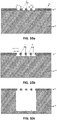
- the hollow trench-like (ring) structure (R1) is created by a method as illustrated in FIG. 10A-10D and FIG. 11A-11F using a pulsed etching technique comprising alternating steps of isotropic etching and passivation (also referred to as "The Bosch process").
- the trench-like structure (R1) is created by first depositing a mask layer (41) on the first main surface (S1) of the substrate (40) as illustrated in FIG. 11A and then defining openings (43) in said mask layer (41) using e.g. state of the art lithography techniques.
- the openings (43) in the deposited layer (41) have a predefined width W mg and the spacing W mb between the openings (43) is maximum 2 times the undercut (scallop) produced during the DRIE process, preferably less. Said undercut depends on the W mg and the DRIE recipe selected. Typically the larger the openings (W mg ) and the higher the etch rate, the higher the undercut will be.
- FIG. 12 and 13 illustrate the relative width of the openings (43). There can be at least two opening as illustrated in FIG. 9B or alternatively there can be several openings as illustrated in FIG. 9A .
- the openings and remaining mask layer should be such that an optimum undercut during the pulsed etching technique is achieved and hence complete removal of substrate material is achieved in order to create only 1 opening (instead of several).
- the trench-like (ring) structure (R1) is fabricated in the substrate (40) by removing substrate material through the openings (43). The alternating steps of isotropic etching and passivation are repeated until the desired depth is achieved. After creation of the trench-like (ring) structure (R1) the openings (43) in the mask layer (41) are closed (sealed) by depositing an additional layer (44) e.g. an oxide such that an airgap (50) is created.
- an additional layer (44) e.g. an oxide such that an airgap (50) is created.
- This processing sequence has the advantage that a thinner dielectric liner (oxide/nitride) will be sufficient for air-gap pinch-off or in other words less sealing material (44) is needed to close the small holes in the mask layer (41). It hence has the advantage that e.g. for wider trench-like structures (R1), e.g. several ⁇ m wide, it avoids the need to deposit a relatively thick oxide layer to seal/close the airgap (50). It further has the advantage that the pinch-off point is less of an issue for sealing the airgap (50).
- the substrate (1) may comprise at least one layer comprising a different material than the rest of the substrate (1) that can be part of the substrate, and may have to be removed partially, for example at the bottom of the inner pillar structure (23 or 50), for example to realize electrical contact with underlying devices, e.g. a PMD layer as illustrated in FIG. 3 and 4 .
- Removing the at least one layer comprising different material can mean e.g., etching it away when removing the inner pillar structure (22).
- each step can be adapted for selectively removing a substrate pillar sub-layer or subsequent sub-layers (for example by changing the etch chemistry in case of dry and/or wet etching.
- a typical example of such a layer is an inter level dielectric (ILD) layer, which is a layer present in a back-end-of-line (BEOL) interconnect structure; having a function of electrically isolating the metal interconnects in the BEOL from for example the front-end-of-line (FEOL).
- ILD inter level dielectric
- BEOL back-end-of-line
- ILD layers or ILD materials are an oxide, e.g. silicon oxide, PSG, SiC, SiN, Tetraethooxysilane (TEOS) Oxide, low-k dielectrics, polymers as BCB or polyimide (epoxy based polymers can be added).
- oxide e.g. silicon oxide, PSG, SiC, SiN, Tetraethooxysilane (TEOS) Oxide, low-k dielectrics, polymers as BCB or polyimide (epoxy based polymers can be added).
- the method according to embodiments of the present invention may further comprise thinning the substrate (1) beforehand (before creation of the trench-like structure and TSV interconnects) from a second main surface (S2) opposite the first main surface (S1).
- the thinning can be performed by for instance mechanical operations such as grinding or other state of the art techniques.
- the thinning may comprise chemically thinning, e.g. by dry/wet etching or plasma etching the substrate (1) from the second main surface (S2),.
- the chemical thinning may not stop at the level where the conductive structure (5) is reached, but may continue above that level (thus slightly over etching the substrate (1), e.g. silicon substrate).
- the interconnect structure (the conducting material (5) or the combined conductive material (5) and dielectric (24)) will then stick out of the etched-back surface, which is advantageous for the addition of a solder volume such as a solder ball or bump.
- a solder volume as for instance a solder ball or solder bump can further be applied to the conductive structure on the second surface.
Landscapes
- Internal Circuitry In Semiconductor Integrated Circuit Devices (AREA)
Claims (13)
- Verfahren zur Herstellung von mindestens einer elektrischen Interconnect-Struktur in einem Substrat, wobei das Verfahren mindestens die folgenden Schritte umfasst:• Bereitstellen eines Substrats (1), das aus Substratmaterial besteht und eine erste Hauptoberfläche (S1) aufweist,• Abscheiden einer Schicht (41), die Öffnungen (43) mit einer Breite Wmg und einem Abstand Wmb zwischen den Öffnungen aufweist,• Fertigen mindestens einer hohlen grabenartigen Struktur (R1) im Substrat (1) von der ersten Hauptoberfläche (S1), wobei die hohle grabenartige Struktur durch Ätzen durch die Öffnungen der Schicht (41) unter Verwendung eines alternierenden isotropischen Ätz-Passivierungsprozesses geschaffen wird und wobei der alternierende isotropische Ätz-Passivierungsprozess wiederholt wird bis die gewünschte Tiefe der grabenartigen Struktur erreicht wird, wobei die grabenartige Struktur eine innere Säulenstruktur (22) von Substratmaterial umgibt,• Abscheiden einer dielektrischen Auskleidung (44), welche die Öffnungen (43) an der ersten Hauptoberfläche (S1) abklemmt, sodass ein Luftspalt in der Mitte der hohlen grabenartigen Struktur (R1) geschaffen wird,• danach Schaffen eines Lochs in der inneren Säule, wodurch ein Silizium-Durchkontaktierungs-, (Through Silicon Via, TSV)-, Loch (23) geschaffen wird, das eine Bodenoberfläche und eine zusätzliche umgebende Struktur (21) aufweist, die aus Material besteht, das sich zwischen dem TSV-Loch (23) und dem Luftspalt in der grabenartigen Struktur (R1) befindet, und• mindestens teilweises Füllen des TSV-Lochs (23) mit einem leitfähigen Material, dadurch Schaffen einer elektrischen Interconnect-Struktur (5), die einen elektrischen Pfad von der Bodenoberfläche des TSV-Lochs (23) hoch bis zur ersten Hauptoberfläche (S1) des Substrats (1) formt.
- Verfahren nach Anspruch 1, wobei ein Abscheiden einer dielektrischen Auskleidung ein Abscheiden einer dielektrischen Auskleidung umfasst, welche die Öffnungen (43) an der ersten Hauptoberfläche (S1) abklemmt, sodass ein Luftspalt geschaffen wird, der die zu bildende elektrische Interconnect-Struktur umgibt.
- Verfahren nach einem der vorstehenden Ansprüche, wobei der alternierende Ätz-Passivierungsprozess vorzugsweise einen SF6-umfassenden Plasmaätzschritt verwendet, der mit einem C4F8-umfassenden Plasmapassivierungsschritt alterniert wird.
- Verfahren nach einem der vorstehenden Ansprüche, wobei die minimale laterale Dicke der abgeschiedenen dielektrischen Auskleidung Wdy größer ist als die halbe maximale Breite des hohlen Teils der grabenartigen Struktur 1/2Wg.
- Verfahren nach einem der vorstehenden Ansprüche, wobei der Schritt eines mindestens teilweisen Füllens des TSV-Lochs mit einem leitfähigen Material durch Füllen des TSV-Lochs mit einem Material ausgeführt wird, das ausgewählt ist aus einem Metall, einer Metalllegierung, einem implantierten Halbleitermaterial, leitfähigem Silizium, leitenden Polymeren, Kohlenstoffnanoröhren, einer Metallpaste und Kombinationen von oben genannten Materialien, unter Verwendung vorzugsweise einer Abscheidungstechnik, die ausgewählt ist aus einer elektrochemischen Abscheidung (ECD) oder alternativ einer chemischen Gasphasenabscheidung (CVD).
- Verfahren nach einem der vorstehenden Ansprüche, wobei das Substrat (1) von einer zweiten Hauptoberfläche (S2) gegenüber der ersten Hauptoberfläche (S1) dünner gemacht wird.
- Verfahren nach einem der vorstehenden Ansprüche, wobei ein Schaffen eines Silizium-Durchkontaktierungs-, (TSV)-, Lochs (23) ein Schaffen eines Silizium-Durchkontaktierungs-, (TSV)-, Lochs (23) umfasst, das eine zusätzliche umgebende Struktur (21) aufweist, die aus Substratmaterial besteht, das sich zwischen dem TSV-Loch (23) und der grabenartigen Struktur (R1) befindet.
- Substrat, umfassend mindestens eine elektrische Interconnect-Struktur, wobei die mindestens eine Interconnect-Struktur umfasst:• eine Interconnect-Struktur in Form einer leitfähigen inneren Säulenstruktur (5), die sich in dem Substrat (1) befindet; und• eine grabenartige Struktur (R1), welche die Interconnect-Struktur (5) umgibt, wobei die grabenartige Struktur (R1) einen Luftspalt (20) umfasst,• dadurch gekennzeichnet, dass die elektrische Interconnect-Struktur eine Maskenschicht (41) mit Öffnungen (43) in der Maskenschicht umfasst, wobei die Öffnungen über der grabenartigen Struktur bereitgestellt sind und dur8ch ein Abdichtungsmaterial (44) abgedichtet sind, das die Öffnungen (43) abklemmt, wodurch der Luftspalt geschaffen wird.
- Substrat nach Anspruch 8, wobei der Luftspalt die elektrische Interconnect-Struktur umgibt.
- Substrat nach einem der Ansprüche 8 oder 9, weiter umfassend eine zusätzliche umgebende Struktur (21), die aus Substratmaterial besteht, das sich zwischen der Interconnect-Struktur (5) und der grabenartigen Struktur (R1) befindet, und das eine Dicke (Breite) WG aufweist, die vorzugsweise größer als 100 nm ist.
- Substrat nach einem der Ansprüche 8 bis 10, wobei die grabenartige Struktur (R1) eine Breite aufweist, die vorzugsweise kleiner ist als 20 µm, oder kleiner als 10 µm, oder kleiner als 7 µm, oder kleiner als 6 µm oder unter 5 µm oder unter 4 µm, oder die variieren kann zwischen 20 µm und 0,5 µm, zwischen 10 µm und 0,5 µm, zwischen 15 µm und 2 µm oder zwischen 10 µm und 3 µm oder zwischen 7 µm und 5 µm, bevorzugter eine Breite von etwa 0,5 µm.
- Substrat nach einem der Ansprüche 8 bis 11, wobei die leitfähige Säule eine Silizium-Durchkontaktierung (TSV) ist und mindestens ein Material umfasst, das ausgewählt ist aus einem Metall, einer Metalllegierung, einem implantierten Halbleitermaterial, leitfähigem Silizium, Kohlenstoffnanoröhren, leitenden Polymeren, einer Metallpaste und Kombinationen von oben genannten Materialien und/oder wobei das Substrat ein Sperrmaterial und/oder Keimmaterial umfasst, wobei sich Grenz- und/oder Keimmaterial an den äußeren Seitenwänden der leitfähigen Säule befindet.
- 3D-gestapelte Halbleitervorrichtung (100), umfassend ein Substrat, das mindestens eine Interconnect-Struktur nach einem der Ansprüche 8 bis 12 umfasst.
Applications Claiming Priority (1)
| Application Number | Priority Date | Filing Date | Title |
|---|---|---|---|
| US36516010P | 2010-07-16 | 2010-07-16 |
Publications (3)
| Publication Number | Publication Date |
|---|---|
| EP2408006A2 EP2408006A2 (de) | 2012-01-18 |
| EP2408006A3 EP2408006A3 (de) | 2013-12-25 |
| EP2408006B1 true EP2408006B1 (de) | 2019-07-03 |
Family
ID=44801921
Family Applications (1)
| Application Number | Title | Priority Date | Filing Date |
|---|---|---|---|
| EP11174114.6A Active EP2408006B1 (de) | 2010-07-16 | 2011-07-15 | Verfahren zur Herstellung von 3D-Interconnectstrukturen mit Luftspalten und zugehöriges Bauelement |
Country Status (2)
| Country | Link |
|---|---|
| US (1) | US8647920B2 (de) |
| EP (1) | EP2408006B1 (de) |
Families Citing this family (65)
| Publication number | Priority date | Publication date | Assignee | Title |
|---|---|---|---|---|
| EP1974376A1 (de) * | 2006-01-18 | 2008-10-01 | STMicroelectronics (Crolles 2) SAS | Integration selbstausgerichteter rahmen zwischen metallleitungen |
| US8314498B2 (en) * | 2010-09-10 | 2012-11-20 | Aptina Imaging Corporation | Isolated bond pad with conductive via interconnect |
| EP2463896B1 (de) * | 2010-12-07 | 2020-04-15 | IMEC vzw | Verfahren zur Herstellung von Substratdurchkontaktierungen, die mit Isolationsgräben mit Luftspalt umgeben sind, sowie zugehöriges Bauelement |
| KR20120067525A (ko) * | 2010-12-16 | 2012-06-26 | 삼성전자주식회사 | 반도체 소자 및 이의 제조 방법 |
| FR2970120A1 (fr) * | 2010-12-31 | 2012-07-06 | St Microelectronics Crolles 2 | Via traversant isole |
| US8753981B2 (en) * | 2011-04-22 | 2014-06-17 | Micron Technology, Inc. | Microelectronic devices with through-silicon vias and associated methods of manufacturing |
| KR101828063B1 (ko) * | 2011-05-17 | 2018-02-09 | 삼성전자주식회사 | 반도체 장치 및 그 형성방법 |
| EP2584598B1 (de) * | 2011-10-20 | 2018-12-05 | ams AG | Verfahren zur Herstellung eines Halbleiterbauelements mit einer Durchkontaktierung und einer Deckschicht und entsprechendes Halbleiterbauelement |
| US8962474B2 (en) * | 2011-11-07 | 2015-02-24 | Globalfoundries Singapore Pte. Ltd. | Method for forming an air gap around a through-silicon via |
| US8779559B2 (en) | 2012-02-27 | 2014-07-15 | Qualcomm Incorporated | Structure and method for strain-relieved TSV |
| JP6035520B2 (ja) * | 2012-04-26 | 2016-11-30 | パナソニックIpマネジメント株式会社 | 半導体装置およびその製造方法 |
| CN102709228A (zh) * | 2012-05-17 | 2012-10-03 | 日月光半导体制造股份有限公司 | 硅穿导孔的制作方法 |
| US10211139B2 (en) * | 2012-05-24 | 2019-02-19 | Unimicron Technology Corp. | Chip package structure |
| US20140103452A1 (en) | 2012-10-15 | 2014-04-17 | Marvell World Trade Ltd. | Isolation components for transistors formed on fin features of semiconductor substrates |
| US20140138790A1 (en) * | 2012-11-21 | 2014-05-22 | Spansion Llc | Inter-Layer Insulator for Electronic Devices and Apparatus for Forming Same |
| US9455188B2 (en) | 2013-01-18 | 2016-09-27 | Globalfoundries Inc. | Through silicon via device having low stress, thin film gaps and methods for forming the same |
| US8900989B2 (en) | 2013-03-06 | 2014-12-02 | Taiwan Semiconductor Manufacturing Company, Ltd. | Method of fabricating an air gap using a damascene process and structure of same |
| DE102013211562B4 (de) | 2013-06-19 | 2024-01-11 | Robert Bosch Gmbh | Verfahren zum Erzeugen einer Metallstruktur in einem Halbleitersubstrat |
| CN104241249B (zh) * | 2013-06-21 | 2017-03-22 | 中芯国际集成电路制造(上海)有限公司 | 硅通孔互连结构及其制作方法 |
| US9236301B2 (en) | 2013-07-11 | 2016-01-12 | Globalfoundries Inc. | Customized alleviation of stresses generated by through-substrate via(S) |
| JP6079502B2 (ja) * | 2013-08-19 | 2017-02-15 | ソニー株式会社 | 固体撮像素子および電子機器 |
| US20150162277A1 (en) * | 2013-12-05 | 2015-06-11 | International Business Machines Corporation | Advanced interconnect with air gap |
| US10177116B2 (en) * | 2014-02-05 | 2019-01-08 | International Business Machines Corporation | Large channel interconnects with through silicon vias (TSVs) and method for constructing the same |
| US10847442B2 (en) * | 2014-02-24 | 2020-11-24 | Micron Technology, Inc. | Interconnect assemblies with through-silicon vias and stress-relief features |
| US9478509B2 (en) * | 2014-03-06 | 2016-10-25 | GlobalFoundries, Inc. | Mechanically anchored backside C4 pad |
| JP6194824B2 (ja) * | 2014-03-18 | 2017-09-13 | 株式会社デンソー | 半導体装置およびその製造方法 |
| JP2016213247A (ja) * | 2015-04-30 | 2016-12-15 | 国立研究開発法人産業技術総合研究所 | 貫通電極及びその製造方法、並びに半導体装置及びその製造方法 |
| US10315915B2 (en) * | 2015-07-02 | 2019-06-11 | Kionix, Inc. | Electronic systems with through-substrate interconnects and MEMS device |
| US9935047B2 (en) | 2015-10-16 | 2018-04-03 | Taiwan Semiconductor Manufacturing Company, Ltd. | Bonding structures and methods forming the same |
| US10410981B2 (en) * | 2015-12-31 | 2019-09-10 | International Business Machines Corporation | Effective medium semiconductor cavities for RF applications |
| CN106960844B (zh) * | 2016-01-11 | 2021-05-18 | 联华电子股份有限公司 | 半导体元件及其制作方法 |
| JP6714825B2 (ja) * | 2016-02-23 | 2020-07-01 | セイコーエプソン株式会社 | 静電気保護回路、半導体集積回路装置、及び、電子機器 |
| US9929290B2 (en) * | 2016-06-20 | 2018-03-27 | Globalfoundries Inc. | Electrical and optical via connections on a same chip |
| US9881867B1 (en) * | 2017-01-19 | 2018-01-30 | Nanya Technology Corporation | Conductive connection structure having stress buffer layer |
| US9991215B1 (en) * | 2017-01-19 | 2018-06-05 | Nanya Technology Corporation | Semiconductor structure with through substrate via and manufacturing method thereof |
| US10256298B2 (en) * | 2017-02-02 | 2019-04-09 | Vanguard International Semiconductor Corporation | Semiconductor structure and method for forming the same |
| US9911652B1 (en) | 2017-03-29 | 2018-03-06 | International Business Machines Corporation | Forming self-aligned vias and air-gaps in semiconductor fabrication |
| DE102017205964A1 (de) * | 2017-04-07 | 2018-10-11 | Robert Bosch Gmbh | Verfahren zur Herstellung einer leitfähigen Durchkontaktierung für ein Substrat sowie leitfähige Durchkontaktierung |
| JP2019075515A (ja) * | 2017-10-19 | 2019-05-16 | ソニーセミコンダクタソリューションズ株式会社 | 半導体装置、撮像装置、製造装置 |
| CN108321118B (zh) * | 2018-04-04 | 2023-10-13 | 长鑫存储技术有限公司 | 导电层间介质空洞的制备方法和半导体器件 |
| US11152294B2 (en) | 2018-04-09 | 2021-10-19 | Corning Incorporated | Hermetic metallized via with improved reliability |
| CN110911370B (zh) * | 2018-09-14 | 2025-02-07 | 长鑫存储技术有限公司 | 硅穿孔结构及其形成方法、半导体器件 |
| US12200875B2 (en) | 2018-09-20 | 2025-01-14 | Industrial Technology Research Institute | Copper metallization for through-glass vias on thin glass |
| DE102019103761A1 (de) * | 2019-02-14 | 2020-08-20 | OSRAM Opto Semiconductors Gesellschaft mit beschränkter Haftung | Verfahren zur herstellung eines bauelements und bauelement |
| US11760682B2 (en) | 2019-02-21 | 2023-09-19 | Corning Incorporated | Glass or glass ceramic articles with copper-metallized through holes and processes for making the same |
| CN110430086B (zh) * | 2019-08-27 | 2020-12-01 | 安徽工程大学 | 基于分时复用的tsv蜂窝单环结构、tsv蜂窝多环结构及容错方法 |
| CN110707068B (zh) * | 2019-09-09 | 2021-10-19 | 长江存储科技有限责任公司 | 半导体互连结构及其制备方法 |
| GB201917734D0 (en) * | 2019-12-04 | 2020-01-15 | Spts Technologies Ltd | Method, substrate and apparatus |
| US11152311B1 (en) | 2020-04-21 | 2021-10-19 | Nanya Technology Corporation | Semiconductor device with protection structure and air gaps and method for fabricating the same |
| JP2022018262A (ja) * | 2020-07-15 | 2022-01-27 | ソニーセミコンダクタソリューションズ株式会社 | 半導体装置、撮像装置および半導体装置の製造方法 |
| CN114242689A (zh) * | 2020-09-09 | 2022-03-25 | 长鑫存储技术有限公司 | 芯片及存储器 |
| EP3996134B1 (de) * | 2020-09-09 | 2024-06-05 | Changxin Memory Technologies, Inc. | Chip und speicher |
| KR20220037093A (ko) | 2020-09-17 | 2022-03-24 | 삼성전자주식회사 | Tsv를 포함하는 반도체 소자 및 이의 제조 방법 |
| JP2024501017A (ja) | 2020-12-28 | 2024-01-10 | アデイア セミコンダクター ボンディング テクノロジーズ インコーポレイテッド | 基板貫通ビアを有する構造体及びそれを形成する方法 |
| KR20230125309A (ko) * | 2020-12-28 | 2023-08-29 | 아데이아 세미컨덕터 본딩 테크놀로지스 인코포레이티드 | 기판-관통 비아를 가지는 구조체 및 이를 형성하기위한 방법 |
| US11574842B2 (en) * | 2021-04-14 | 2023-02-07 | Micron Technology, Inc. | Methods for forming conductive vias, and associated devices and systems |
| US12087729B2 (en) * | 2021-04-30 | 2024-09-10 | Taiwan Semiconductor Manufacturing Company, Ltd. | Multi-chip package having stress relief structure |
| CN115910914B (zh) * | 2021-08-09 | 2025-11-14 | 长鑫存储技术有限公司 | 半导体结构及其制造方法 |
| US20230103023A1 (en) * | 2021-09-24 | 2023-03-30 | Intel Corporation | Semiconductor Die, Semiconductor Device and Method for Forming a Semiconductor Die |
| CN117995795A (zh) * | 2022-10-31 | 2024-05-07 | 华为技术有限公司 | 芯片、芯片堆叠结构、芯片封装结构以及电子设备 |
| CN115621197B (zh) * | 2022-11-22 | 2023-03-14 | 湖北三维半导体集成创新中心有限责任公司 | 一种硅通孔互联的空腔结构及其形成方法 |
| CN116013871A (zh) * | 2022-12-30 | 2023-04-25 | 湖北三维半导体集成创新中心有限责任公司 | 半导体器件及制备方法 |
| US12451411B2 (en) | 2023-01-13 | 2025-10-21 | Globalfoundries U.S. Inc. | Structure with air gaps extending from dielectric liner around through semicondcutor via |
| US20240429127A1 (en) * | 2023-06-23 | 2024-12-26 | Globalfoundries U.S. Inc. | Structure with cavity around through semiconductor via |
| CN120834108B (zh) * | 2025-09-18 | 2025-12-02 | 电子科技大学 | 一种双环减应力槽的高频低应力tsv结构 |
Family Cites Families (9)
| Publication number | Priority date | Publication date | Assignee | Title |
|---|---|---|---|---|
| US6358862B1 (en) * | 1999-09-02 | 2002-03-19 | Micron Technology, Inc | Passivation integrity improvements |
| TW444342B (en) * | 2000-02-17 | 2001-07-01 | United Microelectronics Corp | Manufacturing method of metal interconnect having inner gap spacer |
| DE10205026C1 (de) * | 2002-02-07 | 2003-05-28 | Bosch Gmbh Robert | Halbleitersubstrat mit einem elektrisch isolierten Bereich, insbesondere zur Vertikalintegration |
| US7488680B2 (en) * | 2005-08-30 | 2009-02-10 | International Business Machines Corporation | Conductive through via process for electronic device carriers |
| WO2009050207A1 (en) | 2007-10-15 | 2009-04-23 | Interuniversitair Microelectronica Centrum Vzw | Method for producing electrical interconnects and devices made thereof |
| JP2009181981A (ja) * | 2008-01-29 | 2009-08-13 | Renesas Technology Corp | 半導体装置の製造方法および半導体装置 |
| JP2009272490A (ja) * | 2008-05-08 | 2009-11-19 | Oki Semiconductor Co Ltd | 半導体装置および半導体装置の製造方法 |
| TWI365528B (en) * | 2008-06-27 | 2012-06-01 | Advanced Semiconductor Eng | Semiconductor structure and method for manufacturing the same |
| US20110076853A1 (en) * | 2009-09-28 | 2011-03-31 | Magic Technologies, Inc. | Novel process method for post plasma etch treatment |
-
2011
- 2011-07-14 US US13/183,315 patent/US8647920B2/en active Active
- 2011-07-15 EP EP11174114.6A patent/EP2408006B1/de active Active
Non-Patent Citations (1)
| Title |
|---|
| None * |
Also Published As
| Publication number | Publication date |
|---|---|
| US20120013022A1 (en) | 2012-01-19 |
| EP2408006A3 (de) | 2013-12-25 |
| US8647920B2 (en) | 2014-02-11 |
| EP2408006A2 (de) | 2012-01-18 |
Similar Documents
| Publication | Publication Date | Title |
|---|---|---|
| US8647920B2 (en) | Method for forming 3D-interconnect structures with airgaps | |
| EP2463896B1 (de) | Verfahren zur Herstellung von Substratdurchkontaktierungen, die mit Isolationsgräben mit Luftspalt umgeben sind, sowie zugehöriges Bauelement | |
| US8354737B2 (en) | Small area, robust silicon via structure and process | |
| US9087878B2 (en) | Device with through-silicon via (TSV) and method of forming the same | |
| EP2201600B1 (de) | Verfahren zur herstellung von substratdurchkontaktierungen | |
| US7772123B2 (en) | Through substrate via semiconductor components | |
| US20070128868A1 (en) | Electroplating and electroless plating of conductive materials into openings, and structures obtained thereby | |
| US8455357B2 (en) | Method of plating through wafer vias in a wafer for 3D packaging | |
| TW201041035A (en) | Integrated circuit structure | |
| US10515892B2 (en) | TSV interconnect structure and manufacturing method thereof | |
| TW200951062A (en) | System and method of encapsulation | |
| CN102468156B (zh) | 用于制造半导体芯片的方法以及半导体芯片 | |
| CN101622700A (zh) | 利用电镀的导电过孔形成 | |
| CN101877328A (zh) | 用于制造导电连接的方法 | |
| US9257337B2 (en) | Semiconductor structure and manufacturing method thereof | |
| CN110911383A (zh) | 半导体器件及其制备方法 | |
| US9012325B2 (en) | Method of protecting sidewall surfaces of a semiconductor device | |
| KR101303413B1 (ko) | 마이크로전자 어셈블리 및 그 형성 방법 | |
| JP4552770B2 (ja) | 半導体基板への貫通配線の形成方法 | |
| US9324613B2 (en) | Method for forming through substrate vias with tethers | |
| US7842613B1 (en) | Methods of forming microelectronic packaging substrates having through-substrate vias therein | |
| Jones | Extending Capabilities of Etch and Deposition Technologies for 3D Packaging of Mems in Volume Production | |
| CN108615704A (zh) | 一种硅通孔互连的制作工艺、由此形成的硅通孔互连结构及其应用 | |
| TW201332057A (zh) | 穿矽導通體之製法及結構 |
Legal Events
| Date | Code | Title | Description |
|---|---|---|---|
| AK | Designated contracting states |
Kind code of ref document: A2 Designated state(s): AL AT BE BG CH CY CZ DE DK EE ES FI FR GB GR HR HU IE IS IT LI LT LU LV MC MK MT NL NO PL PT RO RS SE SI SK SM TR |
|
| AX | Request for extension of the european patent |
Extension state: BA ME |
|
| PUAI | Public reference made under article 153(3) epc to a published international application that has entered the european phase |
Free format text: ORIGINAL CODE: 0009012 |
|
| PUAL | Search report despatched |
Free format text: ORIGINAL CODE: 0009013 |
|
| AK | Designated contracting states |
Kind code of ref document: A3 Designated state(s): AL AT BE BG CH CY CZ DE DK EE ES FI FR GB GR HR HU IE IS IT LI LT LU LV MC MK MT NL NO PL PT RO RS SE SI SK SM TR |
|
| AX | Request for extension of the european patent |
Extension state: BA ME |
|
| RIC1 | Information provided on ipc code assigned before grant |
Ipc: H01L 23/48 20060101ALI20131118BHEP Ipc: H01L 21/768 20060101AFI20131118BHEP |
|
| 17P | Request for examination filed |
Effective date: 20140625 |
|
| RBV | Designated contracting states (corrected) |
Designated state(s): AL AT BE BG CH CY CZ DE DK EE ES FI FR GB GR HR HU IE IS IT LI LT LU LV MC MK MT NL NO PL PT RO RS SE SI SK SM TR |
|
| RAP1 | Party data changed (applicant data changed or rights of an application transferred) |
Owner name: IMEC VZW |
|
| GRAP | Despatch of communication of intention to grant a patent |
Free format text: ORIGINAL CODE: EPIDOSNIGR1 |
|
| STAA | Information on the status of an ep patent application or granted ep patent |
Free format text: STATUS: GRANT OF PATENT IS INTENDED |
|
| INTG | Intention to grant announced |
Effective date: 20181218 |
|
| GRAS | Grant fee paid |
Free format text: ORIGINAL CODE: EPIDOSNIGR3 |
|
| GRAJ | Information related to disapproval of communication of intention to grant by the applicant or resumption of examination proceedings by the epo deleted |
Free format text: ORIGINAL CODE: EPIDOSDIGR1 |
|
| GRAL | Information related to payment of fee for publishing/printing deleted |
Free format text: ORIGINAL CODE: EPIDOSDIGR3 |
|
| STAA | Information on the status of an ep patent application or granted ep patent |
Free format text: STATUS: REQUEST FOR EXAMINATION WAS MADE |
|
| GRAR | Information related to intention to grant a patent recorded |
Free format text: ORIGINAL CODE: EPIDOSNIGR71 |
|
| STAA | Information on the status of an ep patent application or granted ep patent |
Free format text: STATUS: GRANT OF PATENT IS INTENDED |
|
| GRAA | (expected) grant |
Free format text: ORIGINAL CODE: 0009210 |
|
| STAA | Information on the status of an ep patent application or granted ep patent |
Free format text: STATUS: THE PATENT HAS BEEN GRANTED |
|
| INTC | Intention to grant announced (deleted) | ||
| AK | Designated contracting states |
Kind code of ref document: B1 Designated state(s): AL AT BE BG CH CY CZ DE DK EE ES FI FR GB GR HR HU IE IS IT LI LT LU LV MC MK MT NL NO PL PT RO RS SE SI SK SM TR |
|
| INTG | Intention to grant announced |
Effective date: 20190524 |
|
| REG | Reference to a national code |
Ref country code: GB Ref legal event code: FG4D |
|
| REG | Reference to a national code |
Ref country code: CH Ref legal event code: EP Ref country code: AT Ref legal event code: REF Ref document number: 1152002 Country of ref document: AT Kind code of ref document: T Effective date: 20190715 |
|
| REG | Reference to a national code |
Ref country code: IE Ref legal event code: FG4D |
|
| REG | Reference to a national code |
Ref country code: DE Ref legal event code: R096 Ref document number: 602011060156 Country of ref document: DE |
|
| REG | Reference to a national code |
Ref country code: NL Ref legal event code: MP Effective date: 20190703 |
|
| REG | Reference to a national code |
Ref country code: LT Ref legal event code: MG4D |
|
| REG | Reference to a national code |
Ref country code: AT Ref legal event code: MK05 Ref document number: 1152002 Country of ref document: AT Kind code of ref document: T Effective date: 20190703 |
|
| PG25 | Lapsed in a contracting state [announced via postgrant information from national office to epo] |
Ref country code: FI Free format text: LAPSE BECAUSE OF FAILURE TO SUBMIT A TRANSLATION OF THE DESCRIPTION OR TO PAY THE FEE WITHIN THE PRESCRIBED TIME-LIMIT Effective date: 20190703 Ref country code: LT Free format text: LAPSE BECAUSE OF FAILURE TO SUBMIT A TRANSLATION OF THE DESCRIPTION OR TO PAY THE FEE WITHIN THE PRESCRIBED TIME-LIMIT Effective date: 20190703 Ref country code: AT Free format text: LAPSE BECAUSE OF FAILURE TO SUBMIT A TRANSLATION OF THE DESCRIPTION OR TO PAY THE FEE WITHIN THE PRESCRIBED TIME-LIMIT Effective date: 20190703 Ref country code: PT Free format text: LAPSE BECAUSE OF FAILURE TO SUBMIT A TRANSLATION OF THE DESCRIPTION OR TO PAY THE FEE WITHIN THE PRESCRIBED TIME-LIMIT Effective date: 20191104 Ref country code: NL Free format text: LAPSE BECAUSE OF FAILURE TO SUBMIT A TRANSLATION OF THE DESCRIPTION OR TO PAY THE FEE WITHIN THE PRESCRIBED TIME-LIMIT Effective date: 20190703 Ref country code: CZ Free format text: LAPSE BECAUSE OF FAILURE TO SUBMIT A TRANSLATION OF THE DESCRIPTION OR TO PAY THE FEE WITHIN THE PRESCRIBED TIME-LIMIT Effective date: 20190703 Ref country code: BG Free format text: LAPSE BECAUSE OF FAILURE TO SUBMIT A TRANSLATION OF THE DESCRIPTION OR TO PAY THE FEE WITHIN THE PRESCRIBED TIME-LIMIT Effective date: 20191003 Ref country code: NO Free format text: LAPSE BECAUSE OF FAILURE TO SUBMIT A TRANSLATION OF THE DESCRIPTION OR TO PAY THE FEE WITHIN THE PRESCRIBED TIME-LIMIT Effective date: 20191003 Ref country code: HR Free format text: LAPSE BECAUSE OF FAILURE TO SUBMIT A TRANSLATION OF THE DESCRIPTION OR TO PAY THE FEE WITHIN THE PRESCRIBED TIME-LIMIT Effective date: 20190703 Ref country code: SE Free format text: LAPSE BECAUSE OF FAILURE TO SUBMIT A TRANSLATION OF THE DESCRIPTION OR TO PAY THE FEE WITHIN THE PRESCRIBED TIME-LIMIT Effective date: 20190703 |
|
| PG25 | Lapsed in a contracting state [announced via postgrant information from national office to epo] |
Ref country code: RS Free format text: LAPSE BECAUSE OF FAILURE TO SUBMIT A TRANSLATION OF THE DESCRIPTION OR TO PAY THE FEE WITHIN THE PRESCRIBED TIME-LIMIT Effective date: 20190703 Ref country code: GR Free format text: LAPSE BECAUSE OF FAILURE TO SUBMIT A TRANSLATION OF THE DESCRIPTION OR TO PAY THE FEE WITHIN THE PRESCRIBED TIME-LIMIT Effective date: 20191004 Ref country code: IS Free format text: LAPSE BECAUSE OF FAILURE TO SUBMIT A TRANSLATION OF THE DESCRIPTION OR TO PAY THE FEE WITHIN THE PRESCRIBED TIME-LIMIT Effective date: 20191103 Ref country code: ES Free format text: LAPSE BECAUSE OF FAILURE TO SUBMIT A TRANSLATION OF THE DESCRIPTION OR TO PAY THE FEE WITHIN THE PRESCRIBED TIME-LIMIT Effective date: 20190703 Ref country code: LV Free format text: LAPSE BECAUSE OF FAILURE TO SUBMIT A TRANSLATION OF THE DESCRIPTION OR TO PAY THE FEE WITHIN THE PRESCRIBED TIME-LIMIT Effective date: 20190703 Ref country code: AL Free format text: LAPSE BECAUSE OF FAILURE TO SUBMIT A TRANSLATION OF THE DESCRIPTION OR TO PAY THE FEE WITHIN THE PRESCRIBED TIME-LIMIT Effective date: 20190703 |
|
| REG | Reference to a national code |
Ref country code: CH Ref legal event code: PL |
|
| PG25 | Lapsed in a contracting state [announced via postgrant information from national office to epo] |
Ref country code: TR Free format text: LAPSE BECAUSE OF FAILURE TO SUBMIT A TRANSLATION OF THE DESCRIPTION OR TO PAY THE FEE WITHIN THE PRESCRIBED TIME-LIMIT Effective date: 20190703 |
|
| REG | Reference to a national code |
Ref country code: BE Ref legal event code: MM Effective date: 20190731 |
|
| PG25 | Lapsed in a contracting state [announced via postgrant information from national office to epo] |
Ref country code: PL Free format text: LAPSE BECAUSE OF FAILURE TO SUBMIT A TRANSLATION OF THE DESCRIPTION OR TO PAY THE FEE WITHIN THE PRESCRIBED TIME-LIMIT Effective date: 20190703 Ref country code: EE Free format text: LAPSE BECAUSE OF FAILURE TO SUBMIT A TRANSLATION OF THE DESCRIPTION OR TO PAY THE FEE WITHIN THE PRESCRIBED TIME-LIMIT Effective date: 20190703 Ref country code: IT Free format text: LAPSE BECAUSE OF FAILURE TO SUBMIT A TRANSLATION OF THE DESCRIPTION OR TO PAY THE FEE WITHIN THE PRESCRIBED TIME-LIMIT Effective date: 20190703 Ref country code: DK Free format text: LAPSE BECAUSE OF FAILURE TO SUBMIT A TRANSLATION OF THE DESCRIPTION OR TO PAY THE FEE WITHIN THE PRESCRIBED TIME-LIMIT Effective date: 20190703 Ref country code: RO Free format text: LAPSE BECAUSE OF FAILURE TO SUBMIT A TRANSLATION OF THE DESCRIPTION OR TO PAY THE FEE WITHIN THE PRESCRIBED TIME-LIMIT Effective date: 20190703 |
|
| PG25 | Lapsed in a contracting state [announced via postgrant information from national office to epo] |
Ref country code: IS Free format text: LAPSE BECAUSE OF FAILURE TO SUBMIT A TRANSLATION OF THE DESCRIPTION OR TO PAY THE FEE WITHIN THE PRESCRIBED TIME-LIMIT Effective date: 20200224 Ref country code: BE Free format text: LAPSE BECAUSE OF NON-PAYMENT OF DUE FEES Effective date: 20190731 Ref country code: SK Free format text: LAPSE BECAUSE OF FAILURE TO SUBMIT A TRANSLATION OF THE DESCRIPTION OR TO PAY THE FEE WITHIN THE PRESCRIBED TIME-LIMIT Effective date: 20190703 Ref country code: LU Free format text: LAPSE BECAUSE OF NON-PAYMENT OF DUE FEES Effective date: 20190715 Ref country code: CH Free format text: LAPSE BECAUSE OF NON-PAYMENT OF DUE FEES Effective date: 20190731 Ref country code: LI Free format text: LAPSE BECAUSE OF NON-PAYMENT OF DUE FEES Effective date: 20190731 Ref country code: MC Free format text: LAPSE BECAUSE OF FAILURE TO SUBMIT A TRANSLATION OF THE DESCRIPTION OR TO PAY THE FEE WITHIN THE PRESCRIBED TIME-LIMIT Effective date: 20190703 Ref country code: SM Free format text: LAPSE BECAUSE OF FAILURE TO SUBMIT A TRANSLATION OF THE DESCRIPTION OR TO PAY THE FEE WITHIN THE PRESCRIBED TIME-LIMIT Effective date: 20190703 |
|
| REG | Reference to a national code |
Ref country code: DE Ref legal event code: R097 Ref document number: 602011060156 Country of ref document: DE |
|
| PLBE | No opposition filed within time limit |
Free format text: ORIGINAL CODE: 0009261 |
|
| STAA | Information on the status of an ep patent application or granted ep patent |
Free format text: STATUS: NO OPPOSITION FILED WITHIN TIME LIMIT |
|
| PG2D | Information on lapse in contracting state deleted |
Ref country code: IS |
|
| PG25 | Lapsed in a contracting state [announced via postgrant information from national office to epo] |
Ref country code: IE Free format text: LAPSE BECAUSE OF NON-PAYMENT OF DUE FEES Effective date: 20190715 |
|
| 26N | No opposition filed |
Effective date: 20200603 |
|
| PG25 | Lapsed in a contracting state [announced via postgrant information from national office to epo] |
Ref country code: SI Free format text: LAPSE BECAUSE OF FAILURE TO SUBMIT A TRANSLATION OF THE DESCRIPTION OR TO PAY THE FEE WITHIN THE PRESCRIBED TIME-LIMIT Effective date: 20190703 |
|
| GBPC | Gb: european patent ceased through non-payment of renewal fee |
Effective date: 20191003 |
|
| PG25 | Lapsed in a contracting state [announced via postgrant information from national office to epo] |
Ref country code: GB Free format text: LAPSE BECAUSE OF NON-PAYMENT OF DUE FEES Effective date: 20191003 |
|
| PG25 | Lapsed in a contracting state [announced via postgrant information from national office to epo] |
Ref country code: CY Free format text: LAPSE BECAUSE OF FAILURE TO SUBMIT A TRANSLATION OF THE DESCRIPTION OR TO PAY THE FEE WITHIN THE PRESCRIBED TIME-LIMIT Effective date: 20190703 |
|
| PG25 | Lapsed in a contracting state [announced via postgrant information from national office to epo] |
Ref country code: HU Free format text: LAPSE BECAUSE OF FAILURE TO SUBMIT A TRANSLATION OF THE DESCRIPTION OR TO PAY THE FEE WITHIN THE PRESCRIBED TIME-LIMIT; INVALID AB INITIO Effective date: 20110715 Ref country code: MT Free format text: LAPSE BECAUSE OF FAILURE TO SUBMIT A TRANSLATION OF THE DESCRIPTION OR TO PAY THE FEE WITHIN THE PRESCRIBED TIME-LIMIT Effective date: 20190703 |
|
| PG25 | Lapsed in a contracting state [announced via postgrant information from national office to epo] |
Ref country code: MK Free format text: LAPSE BECAUSE OF FAILURE TO SUBMIT A TRANSLATION OF THE DESCRIPTION OR TO PAY THE FEE WITHIN THE PRESCRIBED TIME-LIMIT Effective date: 20190703 |
|
| P01 | Opt-out of the competence of the unified patent court (upc) registered |
Effective date: 20230513 |
|
| PGFP | Annual fee paid to national office [announced via postgrant information from national office to epo] |
Ref country code: FR Payment date: 20250620 Year of fee payment: 15 |
|
| PGFP | Annual fee paid to national office [announced via postgrant information from national office to epo] |
Ref country code: DE Payment date: 20250620 Year of fee payment: 15 |
|
| REG | Reference to a national code |
Ref country code: DE Ref legal event code: R079 Ref document number: 602011060156 Country of ref document: DE Free format text: PREVIOUS MAIN CLASS: H01L0021768000 Ipc: H10W0020000000 |