EP2393761B1 - Varistorkeramik - Google Patents
Varistorkeramik Download PDFInfo
- Publication number
- EP2393761B1 EP2393761B1 EP10702118.0A EP10702118A EP2393761B1 EP 2393761 B1 EP2393761 B1 EP 2393761B1 EP 10702118 A EP10702118 A EP 10702118A EP 2393761 B1 EP2393761 B1 EP 2393761B1
- Authority
- EP
- European Patent Office
- Prior art keywords
- proportion
- atom
- varistor
- ceramic
- varistor ceramic
- Prior art date
- Legal status (The legal status is an assumption and is not a legal conclusion. Google has not performed a legal analysis and makes no representation as to the accuracy of the status listed.)
- Active
Links
Images


Classifications
-
- C—CHEMISTRY; METALLURGY
- C04—CEMENTS; CONCRETE; ARTIFICIAL STONE; CERAMICS; REFRACTORIES
- C04B—LIME, MAGNESIA; SLAG; CEMENTS; COMPOSITIONS THEREOF, e.g. MORTARS, CONCRETE OR LIKE BUILDING MATERIALS; ARTIFICIAL STONE; CERAMICS; REFRACTORIES; TREATMENT OF NATURAL STONE
- C04B35/00—Shaped ceramic products characterised by their composition; Ceramics compositions; Processing powders of inorganic compounds preparatory to the manufacturing of ceramic products
- C04B35/01—Shaped ceramic products characterised by their composition; Ceramics compositions; Processing powders of inorganic compounds preparatory to the manufacturing of ceramic products based on oxide ceramics
- C04B35/453—Shaped ceramic products characterised by their composition; Ceramics compositions; Processing powders of inorganic compounds preparatory to the manufacturing of ceramic products based on oxide ceramics based on zinc, tin, or bismuth oxides or solid solutions thereof with other oxides, e.g. zincates, stannates or bismuthates
-
- C—CHEMISTRY; METALLURGY
- C04—CEMENTS; CONCRETE; ARTIFICIAL STONE; CERAMICS; REFRACTORIES
- C04B—LIME, MAGNESIA; SLAG; CEMENTS; COMPOSITIONS THEREOF, e.g. MORTARS, CONCRETE OR LIKE BUILDING MATERIALS; ARTIFICIAL STONE; CERAMICS; REFRACTORIES; TREATMENT OF NATURAL STONE
- C04B35/00—Shaped ceramic products characterised by their composition; Ceramics compositions; Processing powders of inorganic compounds preparatory to the manufacturing of ceramic products
- C04B35/50—Shaped ceramic products characterised by their composition; Ceramics compositions; Processing powders of inorganic compounds preparatory to the manufacturing of ceramic products based on rare-earth compounds
-
- C—CHEMISTRY; METALLURGY
- C04—CEMENTS; CONCRETE; ARTIFICIAL STONE; CERAMICS; REFRACTORIES
- C04B—LIME, MAGNESIA; SLAG; CEMENTS; COMPOSITIONS THEREOF, e.g. MORTARS, CONCRETE OR LIKE BUILDING MATERIALS; ARTIFICIAL STONE; CERAMICS; REFRACTORIES; TREATMENT OF NATURAL STONE
- C04B35/00—Shaped ceramic products characterised by their composition; Ceramics compositions; Processing powders of inorganic compounds preparatory to the manufacturing of ceramic products
- C04B35/622—Forming processes; Processing powders of inorganic compounds preparatory to the manufacturing of ceramic products
- C04B35/62218—Forming processes; Processing powders of inorganic compounds preparatory to the manufacturing of ceramic products obtaining ceramic films, e.g. by using temporary supports
-
- H—ELECTRICITY
- H01—ELECTRIC ELEMENTS
- H01C—RESISTORS
- H01C17/00—Apparatus or processes specially adapted for manufacturing resistors
- H01C17/06—Apparatus or processes specially adapted for manufacturing resistors adapted for coating resistive material on a base
- H01C17/065—Apparatus or processes specially adapted for manufacturing resistors adapted for coating resistive material on a base by thick film techniques, e.g. serigraphy
- H01C17/06506—Precursor compositions therefor, e.g. pastes, inks, glass frits or green body
- H01C17/06513—Precursor compositions therefor, e.g. pastes, inks, glass frits or green body characterised by the resistive component
- H01C17/06533—Precursor compositions therefor, e.g. pastes, inks, glass frits or green body characterised by the resistive component composed of oxides
- H01C17/06546—Oxides of zinc or cadmium
-
- H—ELECTRICITY
- H01—ELECTRIC ELEMENTS
- H01C—RESISTORS
- H01C7/00—Non-adjustable resistors formed as one or more layers or coatings; Non-adjustable resistors made from powdered conducting material or powdered semi-conducting material with or without insulating material
- H01C7/10—Non-adjustable resistors formed as one or more layers or coatings; Non-adjustable resistors made from powdered conducting material or powdered semi-conducting material with or without insulating material voltage responsive, i.e. varistors
- H01C7/1006—Thick film varistors
-
- H—ELECTRICITY
- H01—ELECTRIC ELEMENTS
- H01C—RESISTORS
- H01C7/00—Non-adjustable resistors formed as one or more layers or coatings; Non-adjustable resistors made from powdered conducting material or powdered semi-conducting material with or without insulating material
- H01C7/10—Non-adjustable resistors formed as one or more layers or coatings; Non-adjustable resistors made from powdered conducting material or powdered semi-conducting material with or without insulating material voltage responsive, i.e. varistors
- H01C7/102—Varistor boundary, e.g. surface layers
-
- H—ELECTRICITY
- H01—ELECTRIC ELEMENTS
- H01C—RESISTORS
- H01C7/00—Non-adjustable resistors formed as one or more layers or coatings; Non-adjustable resistors made from powdered conducting material or powdered semi-conducting material with or without insulating material
- H01C7/10—Non-adjustable resistors formed as one or more layers or coatings; Non-adjustable resistors made from powdered conducting material or powdered semi-conducting material with or without insulating material voltage responsive, i.e. varistors
- H01C7/105—Varistor cores
- H01C7/108—Metal oxide
- H01C7/112—ZnO type
-
- H—ELECTRICITY
- H01—ELECTRIC ELEMENTS
- H01C—RESISTORS
- H01C7/00—Non-adjustable resistors formed as one or more layers or coatings; Non-adjustable resistors made from powdered conducting material or powdered semi-conducting material with or without insulating material
- H01C7/18—Non-adjustable resistors formed as one or more layers or coatings; Non-adjustable resistors made from powdered conducting material or powdered semi-conducting material with or without insulating material comprising a plurality of layers stacked between terminals
-
- C—CHEMISTRY; METALLURGY
- C04—CEMENTS; CONCRETE; ARTIFICIAL STONE; CERAMICS; REFRACTORIES
- C04B—LIME, MAGNESIA; SLAG; CEMENTS; COMPOSITIONS THEREOF, e.g. MORTARS, CONCRETE OR LIKE BUILDING MATERIALS; ARTIFICIAL STONE; CERAMICS; REFRACTORIES; TREATMENT OF NATURAL STONE
- C04B2235/00—Aspects relating to ceramic starting mixtures or sintered ceramic products
- C04B2235/02—Composition of constituents of the starting material or of secondary phases of the final product
- C04B2235/30—Constituents and secondary phases not being of a fibrous nature
- C04B2235/32—Metal oxides, mixed metal oxides, or oxide-forming salts thereof, e.g. carbonates, nitrates, (oxy)hydroxides, chlorides
- C04B2235/3205—Alkaline earth oxides or oxide forming salts thereof, e.g. beryllium oxide
- C04B2235/3208—Calcium oxide or oxide-forming salts thereof, e.g. lime
-
- C—CHEMISTRY; METALLURGY
- C04—CEMENTS; CONCRETE; ARTIFICIAL STONE; CERAMICS; REFRACTORIES
- C04B—LIME, MAGNESIA; SLAG; CEMENTS; COMPOSITIONS THEREOF, e.g. MORTARS, CONCRETE OR LIKE BUILDING MATERIALS; ARTIFICIAL STONE; CERAMICS; REFRACTORIES; TREATMENT OF NATURAL STONE
- C04B2235/00—Aspects relating to ceramic starting mixtures or sintered ceramic products
- C04B2235/02—Composition of constituents of the starting material or of secondary phases of the final product
- C04B2235/30—Constituents and secondary phases not being of a fibrous nature
- C04B2235/32—Metal oxides, mixed metal oxides, or oxide-forming salts thereof, e.g. carbonates, nitrates, (oxy)hydroxides, chlorides
- C04B2235/3217—Aluminum oxide or oxide forming salts thereof, e.g. bauxite, alpha-alumina
-
- C—CHEMISTRY; METALLURGY
- C04—CEMENTS; CONCRETE; ARTIFICIAL STONE; CERAMICS; REFRACTORIES
- C04B—LIME, MAGNESIA; SLAG; CEMENTS; COMPOSITIONS THEREOF, e.g. MORTARS, CONCRETE OR LIKE BUILDING MATERIALS; ARTIFICIAL STONE; CERAMICS; REFRACTORIES; TREATMENT OF NATURAL STONE
- C04B2235/00—Aspects relating to ceramic starting mixtures or sintered ceramic products
- C04B2235/02—Composition of constituents of the starting material or of secondary phases of the final product
- C04B2235/30—Constituents and secondary phases not being of a fibrous nature
- C04B2235/32—Metal oxides, mixed metal oxides, or oxide-forming salts thereof, e.g. carbonates, nitrates, (oxy)hydroxides, chlorides
- C04B2235/3224—Rare earth oxide or oxide forming salts thereof, e.g. scandium oxide
- C04B2235/3225—Yttrium oxide or oxide-forming salts thereof
-
- C—CHEMISTRY; METALLURGY
- C04—CEMENTS; CONCRETE; ARTIFICIAL STONE; CERAMICS; REFRACTORIES
- C04B—LIME, MAGNESIA; SLAG; CEMENTS; COMPOSITIONS THEREOF, e.g. MORTARS, CONCRETE OR LIKE BUILDING MATERIALS; ARTIFICIAL STONE; CERAMICS; REFRACTORIES; TREATMENT OF NATURAL STONE
- C04B2235/00—Aspects relating to ceramic starting mixtures or sintered ceramic products
- C04B2235/02—Composition of constituents of the starting material or of secondary phases of the final product
- C04B2235/30—Constituents and secondary phases not being of a fibrous nature
- C04B2235/32—Metal oxides, mixed metal oxides, or oxide-forming salts thereof, e.g. carbonates, nitrates, (oxy)hydroxides, chlorides
- C04B2235/3231—Refractory metal oxides, their mixed metal oxides, or oxide-forming salts thereof
- C04B2235/3241—Chromium oxides, chromates, or oxide-forming salts thereof
-
- C—CHEMISTRY; METALLURGY
- C04—CEMENTS; CONCRETE; ARTIFICIAL STONE; CERAMICS; REFRACTORIES
- C04B—LIME, MAGNESIA; SLAG; CEMENTS; COMPOSITIONS THEREOF, e.g. MORTARS, CONCRETE OR LIKE BUILDING MATERIALS; ARTIFICIAL STONE; CERAMICS; REFRACTORIES; TREATMENT OF NATURAL STONE
- C04B2235/00—Aspects relating to ceramic starting mixtures or sintered ceramic products
- C04B2235/02—Composition of constituents of the starting material or of secondary phases of the final product
- C04B2235/30—Constituents and secondary phases not being of a fibrous nature
- C04B2235/32—Metal oxides, mixed metal oxides, or oxide-forming salts thereof, e.g. carbonates, nitrates, (oxy)hydroxides, chlorides
- C04B2235/327—Iron group oxides, their mixed metal oxides, or oxide-forming salts thereof
- C04B2235/3275—Cobalt oxides, cobaltates or cobaltites or oxide forming salts thereof, e.g. bismuth cobaltate, zinc cobaltite
-
- C—CHEMISTRY; METALLURGY
- C04—CEMENTS; CONCRETE; ARTIFICIAL STONE; CERAMICS; REFRACTORIES
- C04B—LIME, MAGNESIA; SLAG; CEMENTS; COMPOSITIONS THEREOF, e.g. MORTARS, CONCRETE OR LIKE BUILDING MATERIALS; ARTIFICIAL STONE; CERAMICS; REFRACTORIES; TREATMENT OF NATURAL STONE
- C04B2235/00—Aspects relating to ceramic starting mixtures or sintered ceramic products
- C04B2235/02—Composition of constituents of the starting material or of secondary phases of the final product
- C04B2235/30—Constituents and secondary phases not being of a fibrous nature
- C04B2235/32—Metal oxides, mixed metal oxides, or oxide-forming salts thereof, e.g. carbonates, nitrates, (oxy)hydroxides, chlorides
- C04B2235/3284—Zinc oxides, zincates, cadmium oxides, cadmiates, mercury oxides, mercurates or oxide forming salts thereof
-
- C—CHEMISTRY; METALLURGY
- C04—CEMENTS; CONCRETE; ARTIFICIAL STONE; CERAMICS; REFRACTORIES
- C04B—LIME, MAGNESIA; SLAG; CEMENTS; COMPOSITIONS THEREOF, e.g. MORTARS, CONCRETE OR LIKE BUILDING MATERIALS; ARTIFICIAL STONE; CERAMICS; REFRACTORIES; TREATMENT OF NATURAL STONE
- C04B2235/00—Aspects relating to ceramic starting mixtures or sintered ceramic products
- C04B2235/02—Composition of constituents of the starting material or of secondary phases of the final product
- C04B2235/30—Constituents and secondary phases not being of a fibrous nature
- C04B2235/34—Non-metal oxides, non-metal mixed oxides, or salts thereof that form the non-metal oxides upon heating, e.g. carbonates, nitrates, (oxy)hydroxides, chlorides
- C04B2235/3409—Boron oxide, borates, boric acids, or oxide forming salts thereof, e.g. borax
-
- C—CHEMISTRY; METALLURGY
- C04—CEMENTS; CONCRETE; ARTIFICIAL STONE; CERAMICS; REFRACTORIES
- C04B—LIME, MAGNESIA; SLAG; CEMENTS; COMPOSITIONS THEREOF, e.g. MORTARS, CONCRETE OR LIKE BUILDING MATERIALS; ARTIFICIAL STONE; CERAMICS; REFRACTORIES; TREATMENT OF NATURAL STONE
- C04B2235/00—Aspects relating to ceramic starting mixtures or sintered ceramic products
- C04B2235/02—Composition of constituents of the starting material or of secondary phases of the final product
- C04B2235/30—Constituents and secondary phases not being of a fibrous nature
- C04B2235/34—Non-metal oxides, non-metal mixed oxides, or salts thereof that form the non-metal oxides upon heating, e.g. carbonates, nitrates, (oxy)hydroxides, chlorides
- C04B2235/3418—Silicon oxide, silicic acids or oxide forming salts thereof, e.g. silica sol, fused silica, silica fume, cristobalite, quartz or flint
-
- C—CHEMISTRY; METALLURGY
- C04—CEMENTS; CONCRETE; ARTIFICIAL STONE; CERAMICS; REFRACTORIES
- C04B—LIME, MAGNESIA; SLAG; CEMENTS; COMPOSITIONS THEREOF, e.g. MORTARS, CONCRETE OR LIKE BUILDING MATERIALS; ARTIFICIAL STONE; CERAMICS; REFRACTORIES; TREATMENT OF NATURAL STONE
- C04B2235/00—Aspects relating to ceramic starting mixtures or sintered ceramic products
- C04B2235/65—Aspects relating to heat treatments of ceramic bodies such as green ceramics or pre-sintered ceramics, e.g. burning, sintering or melting processes
- C04B2235/656—Aspects relating to heat treatments of ceramic bodies such as green ceramics or pre-sintered ceramics, e.g. burning, sintering or melting processes characterised by specific heating conditions during heat treatment
-
- C—CHEMISTRY; METALLURGY
- C04—CEMENTS; CONCRETE; ARTIFICIAL STONE; CERAMICS; REFRACTORIES
- C04B—LIME, MAGNESIA; SLAG; CEMENTS; COMPOSITIONS THEREOF, e.g. MORTARS, CONCRETE OR LIKE BUILDING MATERIALS; ARTIFICIAL STONE; CERAMICS; REFRACTORIES; TREATMENT OF NATURAL STONE
- C04B2235/00—Aspects relating to ceramic starting mixtures or sintered ceramic products
- C04B2235/70—Aspects relating to sintered or melt-casted ceramic products
- C04B2235/72—Products characterised by the absence or the low content of specific components, e.g. alkali metal free alumina ceramics
Definitions
- a production method for a varistor ceramic according to claim 1 is specified.
- a widespread problem of varistor ceramics is to achieve a low dielectric constant ( ⁇ r ). At the same time a high nonlinearity with sufficient high switching strength in the high current range (ESD, 8/20) and low leakage current should be realized.
- the object is achieved by a method for producing a varistor ceramic according to claim 1. Further embodiments of the manufacturing method for the varistor ceramic are the subject of further claims.
- Varistors are voltage-dependent resistors and are used as surge protection.
- M is Y or Lu.
- the proportion of Co is in a range of 0.1 to 10 atom%, with Co preferably being present as Co 2+ .
- the proportion of Ca is in a range of 0.001 to 5 at.%, With Ca preferably being present as Ca 2+ .
- the proportion of Si is in a range of 0.001 to 0.5 atom%, with Si preferably being present as Si 4+ .
- the proportion of Al is in the range of 0.001 to 0.1 at.%, With Al preferably being present as Al 3+ .
- the amount of Cr ranges from 0.001 to 5 atomic%, with Cr preferably being present as Cr 3+ .
- the amount of B ranges from 0.001 to 5 at.%, With B preferably being present as B 3+ .
- C ⁇ 0 ⁇ r A / d .
- C the capacitance
- ⁇ 0 the permittivity of vacuum
- ⁇ r the relative permittivity
- A the area between two electrodes
- d the thickness of the layer between the electrodes.
- a conventional method of reducing the capacitance of a multilayer varistor is by reducing the area A and increasing the layer thickness d.
- this runs contrary to the multi-layered concept as a Reduction of the area A leads to a reduction in the maximum energy absorption capacity and thus the surge current stability and the robustness with respect to ESD pulses.
- an oxide or salt of the metal M whose cations have a comparatively small ionic radius (eg Y 3+ , Lu 3+ ) is dissolved in the varistor ceramic so that it has a lower capacitance per grain-to-grain contact.
- FIG. 1 shows a schematic flow diagram of the production process of multilayer varistors comprising the following process steps: A1 weighing in, A2 pre-milling, A3 drying, A4 sieving, A5 calcining, A6 regrinding, A7 drying, A8 sieving, B1 caking, B2 green sheets, C1 printing with conductive paste, C2 stacking , C3 cut, D1 decarburization, D2 sintering, E1 application of external termination, E2 burn in.
- FIG. 2 schematically shows the structure of a Dahl lambstors comprising the inner electrodes (1), the varistor ceramic material (2) and the outer termination (3).
- the ceramic body of the multilayer varistor is present as a monolithic ceramic body.
- FIG. 3 shows on the left the characteristic of an ESD pulse and on the right the characteristic of an 8/20 pulse.
- the production of the multilayer varistor can after FIG. 1 respectively.
- a slurry is prepared by addition of a binder, dispersant and a solvent (B1), are drawn from the film with a layer thickness between 5 and 60 microns (B2), which then according to the process diagram in illustration 1 , are processed to multilayer varistors:
- the green sheets are printed with a conductive paste (C1), stacked and then cut (C2, C3).
- the binder is burned out of the green parts in the following decarburization step (D1) at temperatures between 180 ° C and 500 ° C and sintered the components at a temperature between 900 and 1400 ° C (D2). Subsequently, the outer termination layer (E1) is applied and this layer is baked at temperatures between 500 ° C and 1000 ° C (E2).
- the sintering temperature in process step D2) is between 1100 ° C. and 1400 ° C.
- the temperature for the baking in process step E2) is between 600 ° C and 1000 ° C.
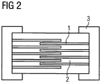
- FIG. 2 shows a schematic side view of a multilayer component.
- the internal electrodes (1) and the layer of the varistor ceramic material (2) follow one another alternately.
- the inner electrodes (1) are alternately connected to one or the other external termination (3). In the middle area overlap the internal electrodes (1).
- FIG. 2 A typical structure of a 0402 multilayer varistor (dimensions 1.0 mm x 0.5 mm x 0.5 mm) shows FIG. 2 : Where the overlap area of the internal electrodes (2) and the number of internal electrodes can be adapted to the desired electrical component properties.
- the electrical characterization of the components was carried out by determining the leakage current, the varistor voltage, the non-linearity coefficient, the 8/20 pulse stability, the ESD pulse stability, the 8/20 terminal voltage at 1 A (U K ).
- FIG. 3 shows left and right respectively a pulse course.
- the current I is plotted against the time t.
- the specific varistor voltage E V is determined at 1 mA.
- the capacitance is measured at 1 V and 1 kHz.
- the ESD stability is achieved with pulses of FIG. 3 left determined: For this purpose, the components with +/- 10 ESD pulses (see FIG. 3 right). The percentage change of U V before and after the pulses and of the leakage current before and after the pulses in percent are calculated and must not have any percentage change of more than 10%. In addition, 8/20 robustness tests (pulse shape see FIG. 3 right). The components were equipped with 8/20 pulses (see FIG. 3 right) at 1 A, 5 A, 10 A, 15 A, 20 A and 25 A, as well as the percentage change of the varistor voltage and the leakage current after the load.
- the proportion of Zn is preferably greater than 90 at%, with Zn preferably being present as Zn 2+ .
- the proportion of Pr is preferably in a range of 0.5 to 0.6 atom%, with Pr preferably being Pr 3+ / 4+ .
- the proportion of M is preferably in the range of 1 to 5 atomic%, with M preferably being present as M 2+ / M 3+ / M 4+ .
- the proportion of Co is preferably in a range of 1.5 to 2.0 at.%, With Co preferably being present as Co 2+ .
- the proportion of Ca is preferably in a range of 0.01 to 0.03 at%, with Ca preferably being present as Ca 2+ .
- the content of Si is preferably in a range of 0.01 to 0.15 atomic%, with Si preferably being present as Si 4+ .
- the content of Al is preferably in a range of 0.005 to 0.01 at.%, With Al being preferably present as Al 3+ .
- the amount of Cr is preferably in a range of 0.05 to 0.2 at%, with Cr being present preferably as Cr 3+ .
- the amount of B is preferably in the range of 0.001 to 0.01 at.%, With B preferably being present as B 3+ .
- the relative permittivity ⁇ r is less than 1000.
- boron oxide can be released from suitable precursors while largely avoiding evaporation losses to control structural formation as a sintering aid in the high temperature range.
- the multilayer varistors of types 0402 and 0201 are characterized by excellent results in leakage current, ESD stability, 8/20 ruggedness, long-term stability and non-linearity.
- the main component is a share of at least 50 atom% to understand.
- the content of Zn is preferably more than 70 atomic%, with Zn preferably being present as Zn 2+ .
- this additionally comprises, between the method steps d) and e), the method step d1) construction of a component.
Landscapes
- Engineering & Computer Science (AREA)
- Microelectronics & Electronic Packaging (AREA)
- Chemical & Material Sciences (AREA)
- Electromagnetism (AREA)
- Physics & Mathematics (AREA)
- Ceramic Engineering (AREA)
- Manufacturing & Machinery (AREA)
- Materials Engineering (AREA)
- Structural Engineering (AREA)
- Organic Chemistry (AREA)
- Inorganic Chemistry (AREA)
- Thermistors And Varistors (AREA)
- Compositions Of Oxide Ceramics (AREA)
Description
- Die Druckschrift "Nahm et al.: The effects of sintering temperature on varistor properties of (Pr, Co, Cr, Y, Al)-doped ZnO ceramics, Materials Letters 62 (2008), 4440-4442)" offenbart eine ZnO-basierte Varistorkeramik mit Dotierungen von Pr in Kombination mit Y sowie weiteren Dotierungen von Co, Cr und Al offenbart.
- Die Druckschrift "Park et al.: Effects of Y2O3 on the microstructure and electrical properties of Pr-ZnO varistors, Journal of Materials Science: Materials in Electronics 16 (2005), 215-219)" offenbart eine ZnO-basierte Varistorkeramik mit Dotierungen von Pr in Kombination mit Y sowie weiteren Dotierungen von Co und Cr.
- Es wird ein Herstellungsverfahren für eine Varistorkeramik nach dem Anspruch 1 angegeben.
- Ein weit verbreitetes Problem von Varistorkeramiken ist es, eine niedrige Dielektrizitätskonstante (εr) zu erzielen. Gleichzeitig soll eine hohe Nichtlinearität bei hinreichender hoher Schaltfestigkeit im Hochstrombereich (ESD, 8/20) und geringem Leckstrom verwirklicht werden.
- Die Aufgabe wird durch ein Verfahren zur Herstellung einer Varistorkeramik nach dem Anspruch 1 gelöst. Weitere Ausführungsformen des Herstellungsverfahrens für die Varistorkeramik sind Gegenstand weiterer Ansprüche.
- Varistoren sind spannungsabhängige Widerstände und werden als Überspannungsschutz eingesetzt.
- Eine Ausführungsform der Erfindung betrifft ein Herstellungsverfahren nach Anspruch 1 für eine Varistorkeramik, welche folgende Materialien umfasst:
- Zn als Hauptbestandteil,
- Pr zu einem Anteil von 0,1 bis 3 Atom-%,
- ein Metall M ausgewählt aus Y, Ho, Er, Yb, Lu zu einem Anteil von 0,1 bis 5 Atom-%; zusätzlich umfassend weitere Materialien, wie beansprucht.
- In einer Ausführungsform steht M für Y oder Lu.
- In einer Ausführungsform liegt der Anteil von Co in einem Bereich von 0,1 bis 10 Atom-%, wobei Co vorzugsweise als Co2+ vorliegt.
- In einer Ausführungsform liegt der Anteil von Ca in einem Bereich von 0,001 bis 5 Atom-%, wobei Ca vorzugsweise als Ca2+ vorliegt.
- In einer Ausführungsform liegt der Anteil von Si in einem Bereich von 0,001 bis 0,5 Atom-%, wobei Si vorzugsweise als Si4+ vorliegt.
- In einer Ausführungsform liegt der Anteil von Al in einem Bereich von 0,001 bis 0,1 Atom-%, wobei Al vorzugsweise als Al3+ vorliegt.
- In einer Ausführungsform liegt der Anteil von Cr in einem Bereich von 0,001 bis 5 Atom-%, wobei Cr vorzugsweise als Cr3+ vorliegt.
- In einer Ausführungsform liegt der Anteil von B in einem Bereich von 0,001 bis 5 Atom-%, wobei B vorzugsweise als B3+ vorliegt.
- Für hohe Übertragungsraten von digitalen Signalen werden Vielschichtvaristoren mit einer hohen ESD-Robustheit und Stoßstromstabilität und einer geringen Kapazität benötigt. Die geringe Kapazität ist notwendig, um das zu übertragende Signal möglichst wenig zu beeinflussen.
- Die Kapazität eines Varistors wird durch die folgende Formel repräsentiert:

- Die wahre Dielektrizitätskonstante εeff für dieses intergranulare Material wird nach Levinson et al. (J. Appl. Phys. Vol. 46; No. 3; 1975) durch folgende Formel beschrieben:

- Eine konventionelle Methode, die Kapazität eines Vielschichtvaristors zu reduzieren (Gl. (1)), erfolgt durch Reduktion der Fläche A und Erhöhung der Schichtdicke d. Dies läuft allerdings dem Vielschichtkonzept zuwider, da eine Reduktion der Fläche A zu einer Reduktion der maximalen Energieaufnahmefähigkeit und damit der Stoßstromstabilität sowie der Robustheit bezüglich ESD-Pulsen führt.
- In einer Ausführungsform umfasst die Varistorkeramik, über Cobaltoxid und Praseodymoxid hinausgehende Zusätze eines Salzes oder Oxids des Metalls M mit geringer Basizität (kleiner Ionenradius), wie zum Beispiel Y3+ oder Lu3+ (rk 3+=93 pm).
- Dadurch wird eine geringere Polarisierbarkeit der Barriere und eine Steuerung der Barriereeigenschaften (Barrierenhöhe und Breite der Verarmungszone) erreicht sowie eine Varistorkeramik mit einer verringerten Kapazität pro Korn-Korn-Kontakt und einer gleichzeitig hohen Nichtlinearität und ESD-Stabilität erhalten.
- Durch die Reduktion der Kapazität pro Korn-Korn-Kontakt können Varistorbauteile mit niedriger Kapazität bei gleicher Fläche zwischen den Elektroden und damit gleich guter ESD-Robustheit und Stoßstromstabilität erhalten werden.
- Im Detail sind die genannten Vorteile in Ausführungsbeispielen beschrieben.
- In einer Ausführungsform ist ein Oxid oder Salz des Metalls M, deren Kationen einen vergleichsweise geringen Ionenradius (z.B. Y3+, Lu3+) aufweisen, im der Varistorkeramik gelöst, so dass diese eine geringere Kapazität pro Korn-Korn-Kontakt aufweist.
- In einem Ausführungsbeispiel werden dem ZnO die Oxide von Praseodym (0.1-3 Atom%) sowie Cobalt (0.1-10 Atom%) als Dotanden und außerdem Kalzium (0.001-5 Atom%), Silizium (0.001-0.5 Atom%), Aluminium (0.001-0.01 Atom%), Chrom (0.001-5 Atom%) in Oxidform sowie Bor in gebundener Form (0.001-5 Atom%) zwecks Steuerung der Gefügeausbildung im Sinterprozess und Yttrium in oxidischer Form (0.1-5 Atom%) zugesetzt.
- Die
Figur 1 zeigt als schematisches Fließschema den Herstellungsprozess von Vielschichtvaristoren umfassend die Verfahrensschritte: A1 Einwaage, A2 Vormahlung, A3 Trocknung, A4 Sieben, A5 Kalzination, A6 Nachmahlung, A7 Trocknung, A8 Sieben, B1 Schlickerbildung, B2 Grünfolien, C1 Bedrucken mit leitfähiger Paste, C2 Stapeln, C3 Cutten, D1 Entkohlung, D2 Sinterung, E1 Aufbringen der Außenterminierung, E2 Einbrennen. - Die
Figur 2 zeigt schematisch den Aufbau eines Vielschichtvaristors umfassend die Innenelektroden (1), das Varistorkeramikmaterial (2) und die Außenterminierung (3). - In einer Ausführungsform liegt der Keramikkörper des Vielschichtvaristors als monolithischer Keramikkörper vor.
- Die
Figur 3 zeigt links die Kennlinie eines ESD-Pulses und rechts die Kennlinie eines 8/20-Pulses.
Die Herstellung des Vielschichtvaristors kann nachFigur 1 erfolgen. - Diese Bestandteile werden in oxidischer, gelöster oder gebundener Form in den in Tabelle 1 genannten Verhältnissen eingewogen (A1), vorgemahlen (A2), getrocknet (A3), gesiebt (A4) und anschließend zwischen 400 °C und 1000 °C kalziniert (A5), nachgemahlen (A6), sprühgetrocknet (A7) und gesiebt (A8).
- Aus dem auf diese Weise hergestellten Pulver wird durch Zugabe eines Binders, Dispergiermittels sowie eines Lösungsmittels ein Schlicker hergestellt (B1), aus dem Folien mit einer Schichtdicke zwischen 5 und 60 µm gezogen werden (B2), die danach nach analog dem Prozessdiagramm in
Abbildung 1 , zu Vielschichtvaristoren verarbeitet werden: Dabei werden die Grünfolien mit einer leitfähigen Paste bedruckt (C1), gestapelt und anschließend gecuttet (C2, C3). - Der Binder wird im folgenden Entkohlungsschritt (D1) aus den Grünteilen bei Temperaturen zwischen 180 °C und 500 °C ausgebrannt und die Bauteile bei einer Temperatur zwischen 900 und 1400 °C gesintert (D2). Anschließend wird die Außenterminierungsschicht (E1) aufgebracht und diese Schicht wird bei Temperaturen zwischen 500 °C und 1000 °C eingebrannt (E2).
- In einer bevorzugten Variante liegt die Sintertemperatur im Verfahrensschritt D2) zwischen 1100 °C und 1400 °C.
- In einer weiteren bevorzugten Variante liegt die Temperatur für das Einbrennen im Verfahrensschritt E2) zwischen 600 °C und 1000 °C.
Figur 2 zeigt in schematischer Seitenansicht ein Vielschichtbauelement. Hierbei folgen die Innenelektroden (1) und die Schicht des Varistorkeramikmaterial (2) alternierend aufeinander. Die Innenelektroden (1) sind abwechselnd jeweils mit der einen bzw. anderen Außenterminierung (3) verbunden. Im Mittleren Bereich überlappen die Innenelektroden (1). - Einen typischen Aufbau eines 0402 Vielschichtvaristors (Abmessungen 1.0 mm x 0.5 mm x 0.5 mm) zeigt
Figur 2 : Wobei die Überlappungsfläche der Innenelektroden (2) sowie die Anzahl der Innenelektroden an die gewünschten elektrischen Bauteileigenschaften angepasst werden können. - Die elektrische Charakterisierung der Bauteile erfolgte durch Bestimmung des Leckstromes, der Varistorspannung, des Nichtlinearitätskoeffizienten, der 8/20-Pulsstabilität, der ESD-Pulsstabilität, der 8/20-Klemmenspannung bei 1 A (UK).
-
Figur 3 zeigt links und rechts jeweils einen Pulsverlauf. Hierbei ist jeweils der Strom I gegen die Zeit t aufgetragen. - Die spezifische Varistorspannung EV wird bei 1 mA bestimmt.
- Die Kapazität wird bei 1 V und 1 kHz gemessen.
- Die ESD-Stabilität wird mit Pulsen der
Figur 3 links bestimmt: Dazu wurden die Bauteile mit +/- 10 ESD-Pulse (sieheFigur 3 rechts) belastet. Die prozentuelle Änderung von UV vor und nach den Pulsen sowie des Leckstromes vor und nach den Pulsen in Prozent werden berechnet und dürfen keine prozentuelle Änderung von mehr als 10 % aufweisen. Außerdem wurden 8/20 Robustheitstests (Pulsform sieheFigur 3 rechts) durchgeführt. Dabei wurden die Bauteile mit 8/20-Pulsen (sieheFigur 3 rechts) bei 1 A, 5 A, 10 A, 15 A, 20 A und 25 A belastet, sowie die prozentuelle Änderung der Varistorspannung und des Leckstrom nach der Belastung bestimmt. - Die Nichtlinearitätskoeffizienten wurden nach den folgenden Gleichungen bestimmt:


- Stabilitätstests wurden unter 80 % AVR bei 125 °C durchgeführt. Wobei der Leckstrom IL unter diesen Bedingungen keine steigende Charakteristik aufweisen sollte.
Tabelle 1 Einwaage: (Einheiten in Atom-%) A B C D Zn 97.9 97.4 96.9 96.4 Co 1.5 1.5 1.5 1.5 Pr 0.5 0.5 0.5 0.5 Cr 0.1 0.1 0.1 0.1 Ca 0.02 0.02 0.02 0.02 Si 0.02 0.02 0.02 0.02 Y 0 0.5 1 1.5 B 0.01 0.01 0.01 0.01 Al 60 ppm 60 ppm 60 ppm 60 ppm Tabelle 2 Elektrische Ergebnisse Material EV [V/mm] εr εr/Ev α1 α2 α3 8/20 Stabilität ESD Stabilität A 268 2200 8.2 11 8 7 > 20 A > 30 kV B 269 1737 7.9 18 10 8 > 20 A > 30 kV C 336 1316 3.7 17 11 9 > 20 A > 30 kV D 525 677 1.3 29 14 11 > 20 A > 30 kV - Die elektrischen Daten sind in Tabelle 2 zusammengefasst. Durch Zugabe von Yttrium steigt die spezifische Varistorspannung von 268 V/mm auf 525 V/mm und gleichzeitig sinkt die relative Permittivität. Diese Änderung ist auf die kornwachstumshemmenden Eigenschaften von Yttriumverbunden zurückzuführen.
- Um einen korngrößenunabhängigen Parameter zu erhalten, wurde das Verhältnis εr/Ev gebildet. Tabelle 2 zeigt, dass dieses Verhältnis mit zunehmender Yttriumzugabe abnimmt. Gleichzeitig werden bei gleich guter Nichtlinearität hohe ESD- und 8/20-Stabilitäten erhalten.
- In einer Ausführungsform liegt der Anteil von Zn vorzugsweise bei größer 90 Atom-%, wobei Zn vorzugsweise als Zn2+ vorliegt.
- In einer Ausführungsform liegt der Anteil von Pr vorzugsweise in einem Bereich von 0,5 bis 0,6 Atom-%, wobei Pr vorzugsweise als Pr3+/4+ vorliegt.
- In einer Ausführungsform liegt der Anteil von M vorzugsweise in einem Bereich von 1 bis 5 Atom-%, wobei M vorzugsweise als M2+ / M3+ / M4+ vorliegt.
- In einer Ausführungsform liegt der Anteil von Co vorzugsweise in einem Bereich von 1,5 bis 2,0 Atom-%, wobei Co vorzugsweise als Co2+ vorliegt.
- In einer Ausführungsform liegt der Anteil von Ca vorzugsweise in einem Bereich von 0,01 bis 0,03 Atom-%, wobei Ca vorzugsweise als Ca2+ vorliegt.
- In einer Ausführungsform liegt der Anteil von Si vorzugsweise in einem Bereich von 0,01 bis 0,15 Atom-%, wobei Si vorzugsweise als Si4+ vorliegt.
- In einer Ausführungsform liegt der Anteil von Al vorzugsweise in einem Bereich von 0,005 bis 0,01 Atom-%, wobei Al vorzugsweise als Al3+ vorliegt.
In einer Ausführungsform liegt der Anteil von Cr vorzugsweise in einem Bereich von 0,05 bis 0,2 Atom-%, wobei Cr vorzugsweise als Cr3+ vorliegt. - In einer Ausführungsform liegt der Anteil von B vorzugsweise in einem Bereich von 0,001 bis 0,01 Atom-%, wobei B vorzugsweise als B3+ vorliegt.
- In einer Ausführungsform liegt die relative Permittivität εr unter 1000.
- In Folge der Vermeidung von Alkalicarbonatzusätzen kann eine hohe Reproduzierbarkeit in der technischen Prozessführung erreicht werden.
- Im Herstellungsverfahren kann Boroxid unter weitgehender Vermeidung von Verdampfungsverlusten zwecks Steuerung von Gefügeausbildung als Sinterhilfsmittel im Bereich hoher Temperaturen aus geeigneten Vorstufen freigesetzt werden.
- Die Vielschichtvaristoren der Bauformen 0402 und 0201 zeichnen sich durch ausgezeichnete Ergebnisse beim Leckstrom, der ESD-Stabilität, 8/20-Robustheit, Langzeitstabilität und Nichtlinearität aus.
- Unter Hauptbestandteil ist ein Anteil von mindestens
50 Atom-% zu verstehen. Der Anteil an Zn beträgt vorzugsweise mehr als 70 Atom-%, wobei Zn vorzugsweise als Zn2+ vorliegt. - In einer Varianten des Herstellungsverfahrens der Varistorkeramik umfasst das Herstellungsverfahren die Verfahrensschritte:
- a) Kalzinieren des Rohkeramikmaterials, b) Herstellung eines Schlickers, c) Fertigen von Grünfolien, d) Entbindern der Grünfolien und e) Sintern der Grünfolien aus d).
- In einer weiteren Variante des Herstellungsverfahrens umfasst dieses zusätzlich zwischen den Verfahrenschritten d) und e) den Verfahrensschritt d1) Aufbauen eines Bauteils.
-
- 1)
- Innenelektrode
- 2)
- Varistorkeramikmaterial
- 3)
- Außenterminierung
Claims (6)
- Verfahren zur Herstellung einer Varistorkeramik, welche folgende Materialien umfasst:- Zn als Hauptbestandteil,- Pr zu einem Anteil von 0,1 bis 3 Atom-%,- ein Metall M ausgewählt aus Y, Ho, Er, Yb, Lu zu einem Anteil von 0,1 bis 5 Atom-%,
zusätzlich umfassend- Co zu einem Anteil von 0,1 bis 10 Atom-%,- Ca zu einem Anteil von 0,001 bis 5 Atom-%,- Si zu einem Anteil von 0,001 bis 0,5 Atom-%,- Al zu einem Anteil von 0,001 bis 0,1 Atom-%,- Cr zu einem Anteil von 0,001 bis 5 Atom-%,- B zu einem Anteil von 0,001 bis 5 Atom-%,umfassend die Verfahrensschritte:a) Kalzinieren des Rohkeramikmaterials,b) Herstellung eines Schlickers,c) Fertigen von Grünfolien,d) Entbindern der Grünfolien,e) Sintern der Grünfolien aus d) bei einer Temperatur von 900 bis 1400 °C. - Verfahren nach Anspruch 1, wobei M für Y oder Lu steht.
- Verfahren nach einem der vorhergehenden Ansprüche, wobei die Varistorkeramik eine relative Permittivität εr von kleiner 2000 aufweist.
- Verfahren nach einem der vorhergehenden Ansprüche, wobei durch den Zusatz von M die relative Permittivität des Varistormaterials reduziert wird.
- Verfahren nach einem der vorhergehenden Ansprüche, wobei die Sintertemperatur zwischen 1000 und 1300 °C liegt.
- Varistorkeramik hergestellt nach einem der vorhergehenden Ansprüche, wobei die Varistorkeramik keine Alkalimetalle aufweist.
Applications Claiming Priority (3)
| Application Number | Priority Date | Filing Date | Title |
|---|---|---|---|
| DE102009007234 | 2009-02-03 | ||
| DE102009023846.8A DE102009023846B4 (de) | 2009-02-03 | 2009-06-04 | Varistorkeramik, Vielschichtbauelement umfassend die Varistorkeramik, Herstellungsverfahren für die Varistorkeramik |
| PCT/EP2010/051188 WO2010089279A2 (de) | 2009-02-03 | 2010-02-01 | Varistorkeramik, vielschichtbauelement umfassend die varistorkeramik, herstellungsverfahren für die varistorkeramik |
Publications (2)
| Publication Number | Publication Date |
|---|---|
| EP2393761A2 EP2393761A2 (de) | 2011-12-14 |
| EP2393761B1 true EP2393761B1 (de) | 2017-04-05 |
Family
ID=42309040
Family Applications (1)
| Application Number | Title | Priority Date | Filing Date |
|---|---|---|---|
| EP10702118.0A Active EP2393761B1 (de) | 2009-02-03 | 2010-02-01 | Varistorkeramik |
Country Status (8)
| Country | Link |
|---|---|
| US (1) | US8487735B2 (de) |
| EP (1) | EP2393761B1 (de) |
| JP (1) | JP5833929B2 (de) |
| KR (1) | KR101667073B1 (de) |
| CN (2) | CN102300832A (de) |
| DE (1) | DE102009023846B4 (de) |
| TW (1) | TWI482180B (de) |
| WO (1) | WO2010089279A2 (de) |
Families Citing this family (4)
| Publication number | Priority date | Publication date | Assignee | Title |
|---|---|---|---|---|
| CN105706189B (zh) * | 2013-11-13 | 2019-05-03 | 日本贵弥功株式会社 | 电子部件及其制造方法 |
| TWI685003B (zh) * | 2018-07-25 | 2020-02-11 | 勝德國際研發股份有限公司 | 壓敏電阻模組 |
| TWI810594B (zh) * | 2021-06-28 | 2023-08-01 | 佳邦科技股份有限公司 | 多層式壓敏電阻及其製作方法 |
| CN115579200A (zh) * | 2021-07-05 | 2023-01-06 | 佳邦科技股份有限公司 | 多层式压敏电阻及其制作方法 |
Family Cites Families (12)
| Publication number | Priority date | Publication date | Assignee | Title |
|---|---|---|---|---|
| JPS60107802A (ja) * | 1983-11-16 | 1985-06-13 | 株式会社富士電機総合研究所 | 電圧非直線抵抗素子 |
| US5640136A (en) | 1992-10-09 | 1997-06-17 | Tdk Corporation | Voltage-dependent nonlinear resistor |
| JPH07320908A (ja) * | 1994-05-19 | 1995-12-08 | Tdk Corp | 酸化亜鉛系バリスタの製造方法および酸化亜鉛系バリスタ |
| CN1046172C (zh) * | 1996-12-31 | 1999-11-03 | 中国科学院等离子体物理研究所 | 氧化锌陶瓷线性电阻器的制造方法 |
| JP2904178B2 (ja) * | 1997-03-21 | 1999-06-14 | 三菱電機株式会社 | 電圧非直線抵抗体及び避雷器 |
| JP3822798B2 (ja) * | 2001-02-16 | 2006-09-20 | 太陽誘電株式会社 | 電圧非直線抵抗体及び磁器組成物 |
| JP4184172B2 (ja) * | 2003-06-30 | 2008-11-19 | Tdk株式会社 | 電圧非直線性抵抗体磁器組成物、電子部品及び積層チップバリスタ |
| CN100394517C (zh) * | 2004-07-10 | 2008-06-11 | 华中科技大学 | ZnO陶瓷薄膜低压压敏电阻的制备方法 |
| CN100382205C (zh) * | 2005-04-26 | 2008-04-16 | 华东师范大学 | 高电位梯度氧化锌压敏电阻材料的制备和应用 |
| KR100821274B1 (ko) * | 2006-07-19 | 2008-04-10 | 조인셋 주식회사 | 칩 세라믹 전자부품 |
| JP4888260B2 (ja) | 2007-07-10 | 2012-02-29 | Tdk株式会社 | 電圧非直線性抵抗体磁器組成物、電子部品、及び積層チップバリスタ |
| JP5088029B2 (ja) * | 2007-07-19 | 2012-12-05 | Tdk株式会社 | バリスタ |
-
2009
- 2009-06-04 DE DE102009023846.8A patent/DE102009023846B4/de active Active
-
2010
- 2010-01-29 TW TW099102532A patent/TWI482180B/zh active
- 2010-02-01 KR KR1020117020443A patent/KR101667073B1/ko active Active
- 2010-02-01 WO PCT/EP2010/051188 patent/WO2010089279A2/de not_active Ceased
- 2010-02-01 US US13/146,450 patent/US8487735B2/en active Active
- 2010-02-01 CN CN2010800060182A patent/CN102300832A/zh active Pending
- 2010-02-01 CN CN201610007173.5A patent/CN105622088A/zh active Pending
- 2010-02-01 JP JP2011546868A patent/JP5833929B2/ja active Active
- 2010-02-01 EP EP10702118.0A patent/EP2393761B1/de active Active
Non-Patent Citations (1)
| Title |
|---|
| None * |
Also Published As
| Publication number | Publication date |
|---|---|
| CN102300832A (zh) | 2011-12-28 |
| TWI482180B (zh) | 2015-04-21 |
| WO2010089279A2 (de) | 2010-08-12 |
| WO2010089279A3 (de) | 2010-10-14 |
| CN105622088A (zh) | 2016-06-01 |
| KR101667073B1 (ko) | 2016-10-17 |
| DE102009023846A1 (de) | 2010-08-05 |
| TW201036003A (en) | 2010-10-01 |
| US20110319255A1 (en) | 2011-12-29 |
| JP2012516825A (ja) | 2012-07-26 |
| JP5833929B2 (ja) | 2015-12-16 |
| US8487735B2 (en) | 2013-07-16 |
| DE102009023846B4 (de) | 2024-02-01 |
| EP2393761A2 (de) | 2011-12-14 |
| KR20110122712A (ko) | 2011-11-10 |
Similar Documents
| Publication | Publication Date | Title |
|---|---|---|
| DE4036997C2 (de) | Monolithischer Varistor | |
| DE69807366T2 (de) | Monolithischer keramischer Kondensator | |
| DE69611642T2 (de) | Zinkoxidkeramik, Verfahren zu deren Herstellung und Zinkoxidvaristoren | |
| DE69304034T2 (de) | Nichtreduzierbare, dielektrische keramische Zusammensetzung | |
| DE69734000T2 (de) | Verfahren zum aufbringen von kontaktbelegungen auf einen träger | |
| DE69710259T2 (de) | Dielektrische keramische Zusammensetzung und ihre Verwendung in einem monolithischen keramischen Kondensator | |
| EP0351004B1 (de) | Nichtlinearer spannungsabhängiger Widerstand | |
| DE69619947T2 (de) | Dielektrische keramische Zusammensetzung und ihre Verwendung für einen monolithischen Kondensator | |
| EP2488468B1 (de) | Widerstandsbauelement umfassend ein keramikmaterial | |
| DE69710265T2 (de) | Dielektrische keramische Zusammensetzung und diese verwendender monolithischer keramischer Kondensator | |
| DE69413613T2 (de) | Metalloxid-Widerstand, Leistungswiderstand und Leistungsschalter | |
| DE4220681C2 (de) | Nichtreduzierende, dielektrische, keramische Zusammensetzung | |
| DE69024340T2 (de) | Halbleiterkeramikkondensator von laminiertem und zwischenkornisolationstyp und verfahren zu seiner herstellung | |
| DE112010003826B4 (de) | Dielektrische keramik und laminierter keramikkondensator | |
| DE102005026731B4 (de) | Mehrschichtchipvaristor | |
| EP0076011A2 (de) | Verfahren zur Herstellung eines Dielektrikums | |
| EP2393761B1 (de) | Varistorkeramik | |
| DE69632001T2 (de) | Verfahren zur Herstellung eines elektrischen Widerstandelements mit nichtlinearen spannungsabhängigen Eigenschaften | |
| EP0040881B1 (de) | Spannungsabhängiger Widerstand und Verfahren zu seiner Herstellung | |
| DE69707247T2 (de) | Keramischer vielschichtkondensator | |
| DE69021809T2 (de) | Verfahren zur herstellung keramischer kondensatoren mit varistor-kennzeichen. | |
| DE2824870A1 (de) | Verfahren zur herstellung eines dielektrikums mit perowskitstruktur | |
| DE3888314T2 (de) | Nichtlineare spannungsabhängige Widerstände. | |
| EP2394276B1 (de) | Varistorkeramik, vielschichtbauelement umfassend die varistorkeramik, herstellungsverfahren für die varistorkeramik | |
| DE112023002807T5 (de) | Temperatursensorelement und Temperatursensor |
Legal Events
| Date | Code | Title | Description |
|---|---|---|---|
| PUAI | Public reference made under article 153(3) epc to a published international application that has entered the european phase |
Free format text: ORIGINAL CODE: 0009012 |
|
| 17P | Request for examination filed |
Effective date: 20110708 |
|
| AK | Designated contracting states |
Kind code of ref document: A2 Designated state(s): AT BE BG CH CY CZ DE DK EE ES FI FR GB GR HR HU IE IS IT LI LT LU LV MC MK MT NL NO PL PT RO SE SI SK SM TR |
|
| DAX | Request for extension of the european patent (deleted) | ||
| 17Q | First examination report despatched |
Effective date: 20130104 |
|
| REG | Reference to a national code |
Ref country code: DE Ref legal event code: R079 Ref document number: 502010013422 Country of ref document: DE Free format text: PREVIOUS MAIN CLASS: C04B0035453000 Ipc: H01C0007100000 |
|
| GRAP | Despatch of communication of intention to grant a patent |
Free format text: ORIGINAL CODE: EPIDOSNIGR1 |
|
| RIC1 | Information provided on ipc code assigned before grant |
Ipc: H01C 7/10 20060101AFI20161031BHEP Ipc: H01C 7/112 20060101ALI20161031BHEP Ipc: C04B 35/453 20060101ALI20161031BHEP Ipc: H01C 7/18 20060101ALI20161031BHEP |
|
| INTG | Intention to grant announced |
Effective date: 20161124 |
|
| GRAS | Grant fee paid |
Free format text: ORIGINAL CODE: EPIDOSNIGR3 |
|
| GRAA | (expected) grant |
Free format text: ORIGINAL CODE: 0009210 |
|
| AK | Designated contracting states |
Kind code of ref document: B1 Designated state(s): AT BE BG CH CY CZ DE DK EE ES FI FR GB GR HR HU IE IS IT LI LT LU LV MC MK MT NL NO PL PT RO SE SI SK SM TR |
|
| REG | Reference to a national code |
Ref country code: GB Ref legal event code: FG4D Free format text: NOT ENGLISH |
|
| REG | Reference to a national code |
Ref country code: CH Ref legal event code: EP |
|
| REG | Reference to a national code |
Ref country code: AT Ref legal event code: REF Ref document number: 882490 Country of ref document: AT Kind code of ref document: T Effective date: 20170415 |
|
| REG | Reference to a national code |
Ref country code: IE Ref legal event code: FG4D Free format text: LANGUAGE OF EP DOCUMENT: GERMAN |
|
| REG | Reference to a national code |
Ref country code: DE Ref legal event code: R096 Ref document number: 502010013422 Country of ref document: DE |
|
| REG | Reference to a national code |
Ref country code: NL Ref legal event code: MP Effective date: 20170405 |
|
| REG | Reference to a national code |
Ref country code: LT Ref legal event code: MG4D |
|
| PG25 | Lapsed in a contracting state [announced via postgrant information from national office to epo] |
Ref country code: NL Free format text: LAPSE BECAUSE OF FAILURE TO SUBMIT A TRANSLATION OF THE DESCRIPTION OR TO PAY THE FEE WITHIN THE PRESCRIBED TIME-LIMIT Effective date: 20170405 |
|
| PG25 | Lapsed in a contracting state [announced via postgrant information from national office to epo] |
Ref country code: ES Free format text: LAPSE BECAUSE OF FAILURE TO SUBMIT A TRANSLATION OF THE DESCRIPTION OR TO PAY THE FEE WITHIN THE PRESCRIBED TIME-LIMIT Effective date: 20170405 Ref country code: NO Free format text: LAPSE BECAUSE OF FAILURE TO SUBMIT A TRANSLATION OF THE DESCRIPTION OR TO PAY THE FEE WITHIN THE PRESCRIBED TIME-LIMIT Effective date: 20170705 Ref country code: GR Free format text: LAPSE BECAUSE OF FAILURE TO SUBMIT A TRANSLATION OF THE DESCRIPTION OR TO PAY THE FEE WITHIN THE PRESCRIBED TIME-LIMIT Effective date: 20170706 Ref country code: HR Free format text: LAPSE BECAUSE OF FAILURE TO SUBMIT A TRANSLATION OF THE DESCRIPTION OR TO PAY THE FEE WITHIN THE PRESCRIBED TIME-LIMIT Effective date: 20170405 Ref country code: FI Free format text: LAPSE BECAUSE OF FAILURE TO SUBMIT A TRANSLATION OF THE DESCRIPTION OR TO PAY THE FEE WITHIN THE PRESCRIBED TIME-LIMIT Effective date: 20170405 Ref country code: LT Free format text: LAPSE BECAUSE OF FAILURE TO SUBMIT A TRANSLATION OF THE DESCRIPTION OR TO PAY THE FEE WITHIN THE PRESCRIBED TIME-LIMIT Effective date: 20170405 |
|
| PG25 | Lapsed in a contracting state [announced via postgrant information from national office to epo] |
Ref country code: PL Free format text: LAPSE BECAUSE OF FAILURE TO SUBMIT A TRANSLATION OF THE DESCRIPTION OR TO PAY THE FEE WITHIN THE PRESCRIBED TIME-LIMIT Effective date: 20170405 Ref country code: LV Free format text: LAPSE BECAUSE OF FAILURE TO SUBMIT A TRANSLATION OF THE DESCRIPTION OR TO PAY THE FEE WITHIN THE PRESCRIBED TIME-LIMIT Effective date: 20170405 Ref country code: IS Free format text: LAPSE BECAUSE OF FAILURE TO SUBMIT A TRANSLATION OF THE DESCRIPTION OR TO PAY THE FEE WITHIN THE PRESCRIBED TIME-LIMIT Effective date: 20170805 Ref country code: SE Free format text: LAPSE BECAUSE OF FAILURE TO SUBMIT A TRANSLATION OF THE DESCRIPTION OR TO PAY THE FEE WITHIN THE PRESCRIBED TIME-LIMIT Effective date: 20170405 Ref country code: BG Free format text: LAPSE BECAUSE OF FAILURE TO SUBMIT A TRANSLATION OF THE DESCRIPTION OR TO PAY THE FEE WITHIN THE PRESCRIBED TIME-LIMIT Effective date: 20170705 |
|
| REG | Reference to a national code |
Ref country code: DE Ref legal event code: R097 Ref document number: 502010013422 Country of ref document: DE |
|
| PG25 | Lapsed in a contracting state [announced via postgrant information from national office to epo] |
Ref country code: DK Free format text: LAPSE BECAUSE OF FAILURE TO SUBMIT A TRANSLATION OF THE DESCRIPTION OR TO PAY THE FEE WITHIN THE PRESCRIBED TIME-LIMIT Effective date: 20170405 Ref country code: RO Free format text: LAPSE BECAUSE OF FAILURE TO SUBMIT A TRANSLATION OF THE DESCRIPTION OR TO PAY THE FEE WITHIN THE PRESCRIBED TIME-LIMIT Effective date: 20170405 Ref country code: EE Free format text: LAPSE BECAUSE OF FAILURE TO SUBMIT A TRANSLATION OF THE DESCRIPTION OR TO PAY THE FEE WITHIN THE PRESCRIBED TIME-LIMIT Effective date: 20170405 Ref country code: SK Free format text: LAPSE BECAUSE OF FAILURE TO SUBMIT A TRANSLATION OF THE DESCRIPTION OR TO PAY THE FEE WITHIN THE PRESCRIBED TIME-LIMIT Effective date: 20170405 Ref country code: CZ Free format text: LAPSE BECAUSE OF FAILURE TO SUBMIT A TRANSLATION OF THE DESCRIPTION OR TO PAY THE FEE WITHIN THE PRESCRIBED TIME-LIMIT Effective date: 20170405 |
|
| PLBE | No opposition filed within time limit |
Free format text: ORIGINAL CODE: 0009261 |
|
| STAA | Information on the status of an ep patent application or granted ep patent |
Free format text: STATUS: NO OPPOSITION FILED WITHIN TIME LIMIT |
|
| PG25 | Lapsed in a contracting state [announced via postgrant information from national office to epo] |
Ref country code: SM Free format text: LAPSE BECAUSE OF FAILURE TO SUBMIT A TRANSLATION OF THE DESCRIPTION OR TO PAY THE FEE WITHIN THE PRESCRIBED TIME-LIMIT Effective date: 20170405 Ref country code: IT Free format text: LAPSE BECAUSE OF FAILURE TO SUBMIT A TRANSLATION OF THE DESCRIPTION OR TO PAY THE FEE WITHIN THE PRESCRIBED TIME-LIMIT Effective date: 20170405 |
|
| 26N | No opposition filed |
Effective date: 20180108 |
|
| PG25 | Lapsed in a contracting state [announced via postgrant information from national office to epo] |
Ref country code: SI Free format text: LAPSE BECAUSE OF FAILURE TO SUBMIT A TRANSLATION OF THE DESCRIPTION OR TO PAY THE FEE WITHIN THE PRESCRIBED TIME-LIMIT Effective date: 20170405 |
|
| REG | Reference to a national code |
Ref country code: CH Ref legal event code: PL |
|
| PG25 | Lapsed in a contracting state [announced via postgrant information from national office to epo] |
Ref country code: MC Free format text: LAPSE BECAUSE OF FAILURE TO SUBMIT A TRANSLATION OF THE DESCRIPTION OR TO PAY THE FEE WITHIN THE PRESCRIBED TIME-LIMIT Effective date: 20170405 Ref country code: MT Free format text: LAPSE BECAUSE OF FAILURE TO SUBMIT A TRANSLATION OF THE DESCRIPTION OR TO PAY THE FEE WITHIN THE PRESCRIBED TIME-LIMIT Effective date: 20170405 |
|
| GBPC | Gb: european patent ceased through non-payment of renewal fee |
Effective date: 20180201 |
|
| REG | Reference to a national code |
Ref country code: DE Ref legal event code: R082 Ref document number: 502010013422 Country of ref document: DE Representative=s name: EPPING HERMANN FISCHER PATENTANWALTSGESELLSCHA, DE Ref country code: DE Ref legal event code: R081 Ref document number: 502010013422 Country of ref document: DE Owner name: TDK ELECTRONICS AG, DE Free format text: FORMER OWNER: EPCOS AG, 81669 MUENCHEN, DE |
|
| REG | Reference to a national code |
Ref country code: IE Ref legal event code: MM4A |
|
| REG | Reference to a national code |
Ref country code: BE Ref legal event code: MM Effective date: 20180228 |
|
| PG25 | Lapsed in a contracting state [announced via postgrant information from national office to epo] |
Ref country code: CH Free format text: LAPSE BECAUSE OF NON-PAYMENT OF DUE FEES Effective date: 20180228 Ref country code: LI Free format text: LAPSE BECAUSE OF NON-PAYMENT OF DUE FEES Effective date: 20180228 Ref country code: LU Free format text: LAPSE BECAUSE OF NON-PAYMENT OF DUE FEES Effective date: 20180201 |
|
| REG | Reference to a national code |
Ref country code: FR Ref legal event code: ST Effective date: 20181031 |
|
| PG25 | Lapsed in a contracting state [announced via postgrant information from national office to epo] |
Ref country code: IE Free format text: LAPSE BECAUSE OF NON-PAYMENT OF DUE FEES Effective date: 20180201 |
|
| PG25 | Lapsed in a contracting state [announced via postgrant information from national office to epo] |
Ref country code: GB Free format text: LAPSE BECAUSE OF NON-PAYMENT OF DUE FEES Effective date: 20180201 Ref country code: BE Free format text: LAPSE BECAUSE OF NON-PAYMENT OF DUE FEES Effective date: 20180228 Ref country code: FR Free format text: LAPSE BECAUSE OF NON-PAYMENT OF DUE FEES Effective date: 20180228 |
|
| REG | Reference to a national code |
Ref country code: AT Ref legal event code: MM01 Ref document number: 882490 Country of ref document: AT Kind code of ref document: T Effective date: 20180201 |
|
| PG25 | Lapsed in a contracting state [announced via postgrant information from national office to epo] |
Ref country code: AT Free format text: LAPSE BECAUSE OF NON-PAYMENT OF DUE FEES Effective date: 20180201 |
|
| PG25 | Lapsed in a contracting state [announced via postgrant information from national office to epo] |
Ref country code: TR Free format text: LAPSE BECAUSE OF FAILURE TO SUBMIT A TRANSLATION OF THE DESCRIPTION OR TO PAY THE FEE WITHIN THE PRESCRIBED TIME-LIMIT Effective date: 20170405 |
|
| PG25 | Lapsed in a contracting state [announced via postgrant information from national office to epo] |
Ref country code: HU Free format text: LAPSE BECAUSE OF FAILURE TO SUBMIT A TRANSLATION OF THE DESCRIPTION OR TO PAY THE FEE WITHIN THE PRESCRIBED TIME-LIMIT; INVALID AB INITIO Effective date: 20100201 Ref country code: PT Free format text: LAPSE BECAUSE OF FAILURE TO SUBMIT A TRANSLATION OF THE DESCRIPTION OR TO PAY THE FEE WITHIN THE PRESCRIBED TIME-LIMIT Effective date: 20170405 |
|
| PG25 | Lapsed in a contracting state [announced via postgrant information from national office to epo] |
Ref country code: MK Free format text: LAPSE BECAUSE OF NON-PAYMENT OF DUE FEES Effective date: 20170405 Ref country code: CY Free format text: LAPSE BECAUSE OF FAILURE TO SUBMIT A TRANSLATION OF THE DESCRIPTION OR TO PAY THE FEE WITHIN THE PRESCRIBED TIME-LIMIT Effective date: 20170405 |
|
| PGFP | Annual fee paid to national office [announced via postgrant information from national office to epo] |
Ref country code: DE Payment date: 20250220 Year of fee payment: 16 |