EP2365281A2 - Capteur de débit angulaire - Google Patents
Capteur de débit angulaire Download PDFInfo
- Publication number
- EP2365281A2 EP2365281A2 EP11154619A EP11154619A EP2365281A2 EP 2365281 A2 EP2365281 A2 EP 2365281A2 EP 11154619 A EP11154619 A EP 11154619A EP 11154619 A EP11154619 A EP 11154619A EP 2365281 A2 EP2365281 A2 EP 2365281A2
- Authority
- EP
- European Patent Office
- Prior art keywords
- angular rate
- rate sensor
- sensor according
- cap
- semiconductor device
- Prior art date
- Legal status (The legal status is an assumption and is not a legal conclusion. Google has not performed a legal analysis and makes no representation as to the accuracy of the status listed.)
- Withdrawn
Links
Images


Classifications
-
- G—PHYSICS
- G01—MEASURING; TESTING
- G01C—MEASURING DISTANCES, LEVELS OR BEARINGS; SURVEYING; NAVIGATION; GYROSCOPIC INSTRUMENTS; PHOTOGRAMMETRY OR VIDEOGRAMMETRY
- G01C19/00—Gyroscopes; Turn-sensitive devices using vibrating masses; Turn-sensitive devices without moving masses; Measuring angular rate using gyroscopic effects
- G01C19/56—Turn-sensitive devices using vibrating masses, e.g. vibratory angular rate sensors based on Coriolis forces
- G01C19/5783—Mountings or housings not specific to any of the devices covered by groups G01C19/5607 - G01C19/5719
-
- G—PHYSICS
- G01—MEASURING; TESTING
- G01C—MEASURING DISTANCES, LEVELS OR BEARINGS; SURVEYING; NAVIGATION; GYROSCOPIC INSTRUMENTS; PHOTOGRAMMETRY OR VIDEOGRAMMETRY
- G01C19/00—Gyroscopes; Turn-sensitive devices using vibrating masses; Turn-sensitive devices without moving masses; Measuring angular rate using gyroscopic effects
- G01C19/56—Turn-sensitive devices using vibrating masses, e.g. vibratory angular rate sensors based on Coriolis forces
-
- H—ELECTRICITY
- H01—ELECTRIC ELEMENTS
- H01L—SEMICONDUCTOR DEVICES NOT COVERED BY CLASS H10
- H01L2224/00—Indexing scheme for arrangements for connecting or disconnecting semiconductor or solid-state bodies and methods related thereto as covered by H01L24/00
- H01L2224/01—Means for bonding being attached to, or being formed on, the surface to be connected, e.g. chip-to-package, die-attach, "first-level" interconnects; Manufacturing methods related thereto
- H01L2224/42—Wire connectors; Manufacturing methods related thereto
- H01L2224/47—Structure, shape, material or disposition of the wire connectors after the connecting process
- H01L2224/48—Structure, shape, material or disposition of the wire connectors after the connecting process of an individual wire connector
- H01L2224/4805—Shape
- H01L2224/4809—Loop shape
- H01L2224/48091—Arched
-
- H—ELECTRICITY
- H01—ELECTRIC ELEMENTS
- H01L—SEMICONDUCTOR DEVICES NOT COVERED BY CLASS H10
- H01L2224/00—Indexing scheme for arrangements for connecting or disconnecting semiconductor or solid-state bodies and methods related thereto as covered by H01L24/00
- H01L2224/01—Means for bonding being attached to, or being formed on, the surface to be connected, e.g. chip-to-package, die-attach, "first-level" interconnects; Manufacturing methods related thereto
- H01L2224/42—Wire connectors; Manufacturing methods related thereto
- H01L2224/47—Structure, shape, material or disposition of the wire connectors after the connecting process
- H01L2224/48—Structure, shape, material or disposition of the wire connectors after the connecting process of an individual wire connector
- H01L2224/481—Disposition
- H01L2224/48135—Connecting between different semiconductor or solid-state bodies, i.e. chip-to-chip
- H01L2224/48137—Connecting between different semiconductor or solid-state bodies, i.e. chip-to-chip the bodies being arranged next to each other, e.g. on a common substrate
-
- H—ELECTRICITY
- H01—ELECTRIC ELEMENTS
- H01L—SEMICONDUCTOR DEVICES NOT COVERED BY CLASS H10
- H01L2224/00—Indexing scheme for arrangements for connecting or disconnecting semiconductor or solid-state bodies and methods related thereto as covered by H01L24/00
- H01L2224/73—Means for bonding being of different types provided for in two or more of groups H01L2224/10, H01L2224/18, H01L2224/26, H01L2224/34, H01L2224/42, H01L2224/50, H01L2224/63, H01L2224/71
- H01L2224/732—Location after the connecting process
- H01L2224/73251—Location after the connecting process on different surfaces
- H01L2224/73265—Layer and wire connectors
-
- H—ELECTRICITY
- H01—ELECTRIC ELEMENTS
- H01L—SEMICONDUCTOR DEVICES NOT COVERED BY CLASS H10
- H01L2224/00—Indexing scheme for arrangements for connecting or disconnecting semiconductor or solid-state bodies and methods related thereto as covered by H01L24/00
- H01L2224/91—Methods for connecting semiconductor or solid state bodies including different methods provided for in two or more of groups H01L2224/80 - H01L2224/90
- H01L2224/92—Specific sequence of method steps
- H01L2224/922—Connecting different surfaces of the semiconductor or solid-state body with connectors of different types
- H01L2224/9222—Sequential connecting processes
- H01L2224/92242—Sequential connecting processes the first connecting process involving a layer connector
- H01L2224/92247—Sequential connecting processes the first connecting process involving a layer connector the second connecting process involving a wire connector
-
- H—ELECTRICITY
- H01—ELECTRIC ELEMENTS
- H01L—SEMICONDUCTOR DEVICES NOT COVERED BY CLASS H10
- H01L2924/00—Indexing scheme for arrangements or methods for connecting or disconnecting semiconductor or solid-state bodies as covered by H01L24/00
- H01L2924/15—Details of package parts other than the semiconductor or other solid state devices to be connected
- H01L2924/151—Die mounting substrate
- H01L2924/153—Connection portion
- H01L2924/1531—Connection portion the connection portion being formed only on the surface of the substrate opposite to the die mounting surface
- H01L2924/15311—Connection portion the connection portion being formed only on the surface of the substrate opposite to the die mounting surface being a ball array, e.g. BGA
Definitions
- the present invention relates to an angular rate sensor and, more particularly, is suitably applied to an angular rate sensor having a function of detecting displacement of a structure present on the inside of a sensor.
- the angular rate sensor is a device that converts an angular rate into an electric signal and detecting the angular rate.
- various physical amounts such as pressure, acceleration, and an angular rate
- angular rate sensor sensors of an oscillation type, a rotation type, a gas type, and an optical type are developed.
- oscillation type and rotation type angular rate sensors employing a silicon microfabrication technique is mainly carried out.
- the oscillation type angular rate sensor is a device that causes an oscillator to oscillate at a predetermined resonant frequency and detects, as an electric signal, displacement of the oscillator involved in angular rate application from the outside.
- the devices employing the silicon microfabrication technique detect displacement of a structure included in a semiconductor device for detecting physical amounts. Therefore, the devices sensitively react to stress or the like applied to the semiconductor device from the outside. In particular, deformation of the semiconductor device due to packaging stress generated when the semiconductor device is packaged causes a measurement error or the like and deteriorates reliability of a sensor device.
- the sensors employing the silicon microfabrication technique indispensably needs to have a packaging structure in which external force is not applied to physical amount detecting units or physical amount detecting devices.
- the sensors are mounted on automobiles, in order to enable mounting of the sensors in a severe environment such as an engine room, it is indispensably necessary to adopt a packaging structure having high reliability.
- JP-A-2004-47897 As a packaging structure of electronic components including semiconductor devices such as the sensors, for example, structures such as an electronic component and an electronic module described in JP-A-2004-47897 and JP-A-2009-33114 are known.
- the electronic component described in JP-A-2004-47897 has a configuration in which a piezoelectric element and an electronic component are packaged on a metallic core board and covered with a metal cap connected by soldering to core metal of the metallic core board and sealing resin is filled on the inner side of the metal cap.
- the electronic module described in JP-A-2009-33114 has a configuration in which an electronic component is packaged on a multilayer board and covered with a metal shield electrically connected to a ground electrode of the multilayer board and the inner side of the metal shield is sealed by epoxy resin or the like.
- a semiconductor device for detecting an angular rate fixed on a core metal layer of a metallic core board having a core metal layer formed of a metal plate and a wiring layer including a wiring structure is disposed in a hollow chamber formed by a cap fixed on the wiring layer, the core metal layer formed of the metal plate, and the metallic core board.
- the semiconductor device, the metallic core board, and the cap are molded with resin.
- the present invention it is possible to reduce stress applied to the semiconductor device for detecting an angular rate. Therefore, it is possible to reduce a measurement error and the like of a sensor and secure reliability.
- the sensor has a structure that can improve electromagnetic noise resistance and moisture resistance. It is possible to provide a highly reliable angular rate sensor.
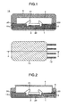
- Figs. 1 and 2 are sectional schematic views of an angular rate sensor according to the present invention.
- an angular rate sensor 15 includes a metallic core board 2 including a core metal layer 1 formed substantially by a metal plate having thickness of, for example 0.5 mm and a wiring layer 18 of a multilayer structure including a wiring structure (an electrically conductive wiring pattern embedded in or arranged on a plastic layer), a semiconductor device 3 for detecting an angular rate, bonding wires 21 that electrically connect the semiconductor device 3 and the wiring layer 18 to each other, a cap 4 fixed onto the wiring layer 18, lead terminals 13 for extracting a signal of the semiconductor device 3 for detecting an angular rate, and resin for molding the entire angular rate sensor 15.
- a metallic core board 2 including a core metal layer 1 formed substantially by a metal plate having thickness of, for example 0.5 mm and a wiring layer 18 of a multilayer structure including a wiring structure (an electrically conductive wiring pattern embedded in or arranged on a plastic layer), a semiconductor device 3 for detecting an angular rate, bonding wires 21 that electrically connect the semiconductor device 3 and the wiring
- the angular rate sensor 15 is formed in a structure in which the core metal layer 1 is exposed by providing a cavity in the wiring layer 18 of the metallic core board 2, which includes the core metal layer 1 made of the metal plate or the like having thickness of, for example, 0.5 mm and the wiring layer 18, the semiconductor device 3 for detecting an angular rate is die-bonded to the exposed core metal layer 1 by an adhesive (resin) 20, and the semiconductor device 3 and the wiring layer 18 are electrically connected by the bonding wires 21.
- the semiconductor device 3 is fixed on the core metal layer 1 having strength higher than that of the wiring layer 18. Therefore, it is possible to reduce packaging stress applied to the semiconductor device 3 such as bending by molding.
- the angular rate sensor 15 may include a semiconductor device (not shown) for detecting acceleration in the same place as the semiconductor 3 for detecting an angular rate and have a function of detecting acceleration.
- the angular rate sensor 15 may be formed in a structure having high moisture resistance in which the cap 4 is fixed to the wiring layer 18 of the metallic core board 2 by the adhesive 20, whereby the cap 4 and the metallic core board 2 form a hollow chamber, and the semiconductor device 3 is disposed in the hollow chamber, whereby the semiconductor device 3 is substantially entirely covered with metal and not in contact with the external air.
- the angular rate sensor 15 may be formed in a structure having higher moisture resistance by filling inert gas such as nitrogen gas (not shown) in the hollow chamber formed by the cap 4 and the metallic core board 2.
- the angular rate sensor 15 may be formed in a structure having a higher moisture resistance by disposing a getter material for moisture absorption such as silica gel (not shown) in the hollow chamber formed by the cap 4 and the metallic core board 2.
- a getter material for moisture absorption such as silica gel (not shown)
- the wiring layer 18 and the cap 4 receives external force such as packaging stress, whereby it is possible to reduce external force application to the semiconductor device 3 fixed on the core metal layer 1. Therefore, the angular rate sensor 15 is formed in a structure in which moisture resistance is further improved while the external force application to the semiconductor device 3 is reduced by mold-sealing, with resin 5, the outer side of the hollow chamber formed by the cap 4 and the metallic core board 2.
- the angular rate sensor 15 may be formed in a structure in which a range mold-sealed by the resin 5 is set only in, for example, a metal cap attaching portion to limit the range to be mold-sealed, whereby packaging stress such as bending to be applied is limited and the stress application to the semiconductor device 3 is further reduced.
- Fig. 3 is a sectional schematic view of the angular rate sensor according to the present invention.
- the angular rate sensor 15 is formed in a structure including means for improving electromagnetic noise resistance by die-bonding, with the adhesive 20, a single processing device 9 for performing amplification and the like of a signal to the exposed core metal layer 1 and stabilizing rear surface potential of the signal processing device 9 and processing a signal from the semiconductor device 3 by electrically connecting the signal processing device 9 to the semiconductor device 3 and the wiring layer 18 with a boding wire 21.
- the angular rate sensor 15 may be formed in a structure in which the signal processing device 9 is die-bonded to the exposed core metal layer 1 by the adhesive 20 and the semiconductor device 3 is stacked and fixed on the signal processing device 9 by the adhesive 20 and a structure in which it is possible to reduce a packaging area while improving electromagnetic noise resistance of the signal processing device 9 by electrically connecting the signal processing device 9, the semiconductor device 3, and the wiring layer 18 to one another with the bonding wires 21.
- the angular rate sensor 15 is formed in a structure in which moisture resistance is further improved by potting gel 17 on the semiconductor device 3 and the signal processing device 9 disposed in the hollow chamber formed by the cap 4 and the metallic core board 2.
- Fig. 6 is a sectional schematic view of the angular rate sensor according to the present invention.
- Fig. 7 is a schematic diagram including a perspective view of only a conductor pattern 7 excluding the cap 4, the resin 5, and a conductive joining material 22 of the angular rate sensor according to the present invention.
- the angular rate sensor 15 is formed in a structure in which the conductor pattern 7 is provided so as to surround the semiconductor device 3 on the front surface of the wiring layer 18, the cap 4 made of a metal material such as aluminum or a 42 alloy is joined to the conductor pattern 7 by the conductive joining material 22 such as solder or a conductive adhesive, and the conductor pattern 7 is connected to a ground side through a via line 6 and a pad 10 provided on the metallic core board 2, whereby, since the semiconductor device 3 is surrounded by a metal material connected to the ground side, electromagnetic noise resistance and moisture resistance are improved.
- the lead terminals 13 may be connected to the pad 10 and the conductor pattern 7 may be connected to the ground side using the lead terminals 13.
- the angular rate sensor 15 may be formed in a structure in which, to make the via line 6 and the pad 10 of the metallic core board 2 unnecessary, a cavity is provided to surround the semiconductor device 3 on the front surface of the wiring layer 18, the core metal layer 1 is exposed, the cap 4 made of the metal material is joined to the exposed core metal layer 1 by the conductive joining material 22 such as solder or a conductive adhesive, and the core metal layer 1 is connected to the ground side, whereby the semiconductor device 3 is surrounded by the metal material connected to the ground side and electromagnetic noise resistance and moisture resistance are improved.
- the angular rate sensor 15 is formed in such a structure, since the wiring layer 18 in a portion surrounded by the cavity is formed as an island pattern, it is extremely difficult to manufacture the metallic core board 2 having a multilayer structure.
- Fig. 8 is a sectional schematic view of the angular rate sensor according to the present invention.
- the angular rate sensor according to the present invention is formed in a structure in which the semiconductor device 3 for detecting an angular rate is die-bonded to the exposed core metal layer 1 by the adhesive 20, the semiconductor device 3 and pads 10 provided on the wiring layer 18 are electrically connected by the bonding wires 21, via holes 16 in at least one or more places are opened in the core metal layer 1 of the metallic core board 2, via lines 6 are inserted through the via holes 16, and the pads 10 provided on the front surface of the wiring layer 18, internal wires 11 provided in the metallic core board 2, and the pads 10 provided on the rear surface of the metallic core board 2 are electrically connected, whereby a signal of the semiconductor device 3 can be extracted from the pads 10 provided on the rear surface of the metallic core board 2.
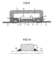
- Fig. 9 is a sectional schematic view of the angular rate sensor according to the present invention.
- Figs. 10 , 11, and 12 are packaging schematic diagrams of the angular rate sensor according to the present invention.
- the angular rate sensor is formed in a structure in which the lead terminals 13 are connected to the pads 10 provided on the rear surface of the metallic core board 2 and an output of the semiconductor device 3 can be extracted from the lead terminals 13. Therefore, as shown in Fig. 10 , the angular rate sensor is formed in a structure in which the lead terminals 13 are joined to a packaging board 14 such as a printed board using the conductive joining material 22 such as solder and the conductive joining material 22 and the lead terminal 13 receive external force such as deformation or distortion of the packaging board 14 due to thermal stress, whereby it is possible to reduce external force application to the semiconductor device 3 in the angular rate sensor 15.
- a packaging board 14 such as a printed board using the conductive joining material 22 such as solder and the conductive joining material 22 and the lead terminal 13 receive external force such as deformation or distortion of the packaging board 14 due to thermal stress, whereby it is possible to reduce external force application to the semiconductor device 3 in the angular rate sensor 15.
- the angular rate sensor according to the present invention when the angular rate sensor according to the present invention is mounted on an automobile, the angular rate sensor is often mounted on the packaging board 14 fixed by board holders 25 in a control unit 8 included in an engine room wall 12.
- the packaging board 14 in the control unit 8 is often fixed in a state in which the packaging board 14 stands vertically with respect to the ground 19.
- the angular rate sensor according to the present invention is formed in a structure in which the lead terminals 13 are bent and joined to the packaging board 14 using the conductive joining material 22 such as solder, whereby it is possible to mount the angular rate sensor 15 in the control unit 8 without changing a detection axis of the angular rate sensor 15.
- the angular rate sensor according to the present invention is formed in a structure in which, even when the packaging board 14 mounted with the angular rate sensor is fixed in a state oblique to the ground 19, the lead terminals 13 are bent and joined to the packaging board 14 using the conductive joining material 22 such as solder, whereby it is possible to mount the angular rate sensor 15 in the control unit 8 without changing the detection axis of the angular rate sensor 15.
- the angular rate sensor according to the present invention may be formed in a structure in which a holder 23 made of metal is bonded to the packaging board 14 and the angular rate sensor 15 by the adhesive, whereby shift of a mounting angle can be prevented.
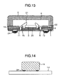
- Fig. 13 is a sectional schematic view of the angular rate sensor according to the present invention.
- Fig. 14 is a packaging schematic diagram of the angular rate sensor according to the present invention.
- the angular rate sensor according to the present invention is formed in a structure in which solder balls 24 are connected to the pads 10 provided on the rear surface of the metallic core board 2 and an output of the semiconductor device 3 can be extracted from the solder balls 24. Therefore, as shown in Fig. 14 , the angular rate sensor is formed in a structure in which the angular rate sensor 15 is bonded to the packaging board 14 such as a printed board using the solder balls 24, whereby it is possible to reduce a packaging area. It is also possible to mount the angular rate sensor according to the present invention in a limited space such as the inside of a cabin or an engine room of an automobile.
- Figs. 15A to 15D are sectional schematic views showing a manufacturing process for the angular rate sensor according to the present invention.
- the metallic core board 2 including the core metal layer 1 made of the metal board and the wiring layer 18 of the multilayer structure including the wiring structure is prepared.
- the semiconductor device 3 for detecting an angular rate is die-bonded by the adhesive 20 to the core metal layer 1 exposed by the cavity provided in the wiring layer 18 of the metallic core board 2.
- a board sheet formed by connecting a large number of metallic core boards 2 may be prepared.
- Packaging stress or the like applied to the semiconductor device 3 may be reduced by die-bonding the semiconductor device 3 with, for example, the soft adhesive 20 such as a silicon adhesive.
- step b in Fig. 15 the semiconductor device 3 and the wiring layer 18 are electrically connected by the bonding wires 21.
- the cap 4 is fixed to the wiring layer 18 of the metallic core board 2 by the adhesive 20, whereby a hollow chamber is formed by the cap 4 and the metallic core board 2.
- inert gas such as nitrogen gas (not shown)
- the cap 4 may be fixed in a state in which the gas is filled in the hollow chamber.
- step d in Fig. 15 the outer side of the hollow chamber formed by the cap 4 and the metallic core board 2 is mold-sealed by the resin 5.
Landscapes
- Physics & Mathematics (AREA)
- Engineering & Computer Science (AREA)
- General Physics & Mathematics (AREA)
- Radar, Positioning & Navigation (AREA)
- Remote Sensing (AREA)
- Gyroscopes (AREA)
- Pressure Sensors (AREA)
Applications Claiming Priority (1)
| Application Number | Priority Date | Filing Date | Title |
|---|---|---|---|
| JP2010055226A JP5463173B2 (ja) | 2010-03-12 | 2010-03-12 | 角速度検出装置 |
Publications (2)
| Publication Number | Publication Date |
|---|---|
| EP2365281A2 true EP2365281A2 (fr) | 2011-09-14 |
| EP2365281A3 EP2365281A3 (fr) | 2016-08-17 |
Family
ID=44185641
Family Applications (1)
| Application Number | Title | Priority Date | Filing Date |
|---|---|---|---|
| EP11154619.8A Withdrawn EP2365281A3 (fr) | 2010-03-12 | 2011-02-16 | Capteur de débit angulaire |
Country Status (3)
| Country | Link |
|---|---|
| US (1) | US8459108B2 (fr) |
| EP (1) | EP2365281A3 (fr) |
| JP (1) | JP5463173B2 (fr) |
Cited By (2)
| Publication number | Priority date | Publication date | Assignee | Title |
|---|---|---|---|---|
| CN102393191A (zh) * | 2011-11-18 | 2012-03-28 | 郑州煤矿机械集团股份有限公司 | 矿用本安型双轴倾角传感器 |
| EP3441771A1 (fr) * | 2017-08-10 | 2019-02-13 | Seiko Epson Corporation | Capteur de quantité physique, unité de mesure de l'inertie, appareil électronique et véhicule |
Families Citing this family (11)
| Publication number | Priority date | Publication date | Assignee | Title |
|---|---|---|---|---|
| EP2375219B1 (fr) * | 2009-04-17 | 2019-02-20 | Hitachi, Ltd. | Capteur d'inertie et procédé pour la fabrication de celui-ci |
| ITTO20110876A1 (it) * | 2011-09-30 | 2013-03-31 | Stmicroelectronics Malta Ltd | Metodo di saldatura di un cappuccio ad uno strato di supporto |
| US20130201316A1 (en) | 2012-01-09 | 2013-08-08 | May Patents Ltd. | System and method for server based control |
| DE102014213217A1 (de) * | 2014-07-08 | 2016-01-14 | Continental Teves Ag & Co. Ohg | Körperschallentkopplung an mit Geberfeldern arbeitenden Sensoren |
| JP6597069B2 (ja) * | 2015-09-02 | 2019-10-30 | セイコーエプソン株式会社 | センサーユニット、電子機器、および移動体 |
| EP3652721A1 (fr) | 2017-09-04 | 2020-05-20 | NNG Software Developing and Commercial LLC | Procédé et appareil de collecte et d'utilisation de données de capteur provenant d'un véhicule |
| EP3888346A4 (fr) | 2019-02-19 | 2022-08-24 | Edgy Bees Ltd. | Estimation d'un retard en temps réel d'un flux de données vidéo |
| CN111627867A (zh) * | 2019-02-28 | 2020-09-04 | 富泰华工业(深圳)有限公司 | 芯片封装结构及其制作方法 |
| JP2022046921A (ja) | 2020-09-11 | 2022-03-24 | セイコーエプソン株式会社 | 電子デバイスの製造方法 |
| JP2022046922A (ja) | 2020-09-11 | 2022-03-24 | セイコーエプソン株式会社 | 電子デバイス |
| JP2022046920A (ja) | 2020-09-11 | 2022-03-24 | セイコーエプソン株式会社 | 電子デバイス |
Citations (2)
| Publication number | Priority date | Publication date | Assignee | Title |
|---|---|---|---|---|
| JP2004047897A (ja) | 2002-07-15 | 2004-02-12 | Hitachi Ltd | 電子部品および電子部品の製造方法 |
| JP2009033114A (ja) | 2007-06-29 | 2009-02-12 | Tdk Corp | 電子モジュール、及び電子モジュールの製造方法 |
Family Cites Families (22)
| Publication number | Priority date | Publication date | Assignee | Title |
|---|---|---|---|---|
| JPH07211812A (ja) * | 1994-01-25 | 1995-08-11 | Toppan Printing Co Ltd | 多層リードフレーム |
| JPH08327655A (ja) * | 1995-06-01 | 1996-12-13 | Matsushita Electric Ind Co Ltd | 加速度センサ |
| JPH098175A (ja) * | 1995-06-14 | 1997-01-10 | Fuji Kiko Denshi Kk | 多層プリント基板のボンディング用棚形成方法 |
| JP3636534B2 (ja) * | 1996-04-08 | 2005-04-06 | 松下電器産業株式会社 | 力学量センサおよびその製造法 |
| JP3646776B2 (ja) * | 1999-03-16 | 2005-05-11 | 株式会社村田製作所 | 電子部品 |
| JP2001110928A (ja) * | 1999-10-04 | 2001-04-20 | Shinko Electric Ind Co Ltd | 半導体パッケージの製造方法 |
| JP3733419B2 (ja) * | 2001-07-17 | 2006-01-11 | 日立エーアイシー株式会社 | 電子部品内蔵型多層基板とその製造方法及びそれに使用するメタルコア基板 |
| JP3838907B2 (ja) * | 2001-12-03 | 2006-10-25 | Necエレクトロニクス株式会社 | 半導体装置 |
| JP2004064912A (ja) * | 2002-07-30 | 2004-02-26 | Hitachi Ltd | 自動車制御装置 |
| JP3938017B2 (ja) * | 2002-11-21 | 2007-06-27 | 株式会社日立製作所 | 電子装置 |
| JP4156946B2 (ja) * | 2003-02-26 | 2008-09-24 | 三菱電機株式会社 | 加速度センサ |
| JP2005106481A (ja) * | 2003-09-26 | 2005-04-21 | Seiko Epson Corp | 圧電振動ジャイロ素子及び圧電振動ジャイロセンサ |
| JP2006080397A (ja) * | 2004-09-10 | 2006-03-23 | Sumitomo Metal Electronics Devices Inc | 高放熱型プラスチックパッケージ及びその製造方法 |
| JP2006153799A (ja) * | 2004-12-01 | 2006-06-15 | Denso Corp | 角速度センサ装置およびその製造方法 |
| JP4724488B2 (ja) * | 2005-02-25 | 2011-07-13 | 日立オートモティブシステムズ株式会社 | 集積化マイクロエレクトロメカニカルシステム |
| JP2007071677A (ja) | 2005-09-07 | 2007-03-22 | Hitachi Ltd | コンバインドセンサとその製造方法 |
| JP4915548B2 (ja) * | 2005-12-22 | 2012-04-11 | パナソニック株式会社 | 立体回路基板の製造方法 |
| JP4935126B2 (ja) * | 2006-03-15 | 2012-05-23 | パナソニック株式会社 | 角速度センサ |
| JP2007166899A (ja) * | 2007-02-09 | 2007-06-28 | Hitachi Ltd | 自動車制御装置 |
| JP4481323B2 (ja) | 2007-07-20 | 2010-06-16 | 日立オートモティブシステムズ株式会社 | 物理量センサ及びその製造方法 |
| JP2009041962A (ja) * | 2007-08-07 | 2009-02-26 | Murata Mfg Co Ltd | 外力検知装置およびその製造方法 |
| JP5277755B2 (ja) * | 2008-07-01 | 2013-08-28 | オムロン株式会社 | 電子部品 |
-
2010
- 2010-03-12 JP JP2010055226A patent/JP5463173B2/ja not_active Expired - Fee Related
-
2011
- 2011-02-16 EP EP11154619.8A patent/EP2365281A3/fr not_active Withdrawn
- 2011-02-17 US US13/029,520 patent/US8459108B2/en active Active
Patent Citations (2)
| Publication number | Priority date | Publication date | Assignee | Title |
|---|---|---|---|---|
| JP2004047897A (ja) | 2002-07-15 | 2004-02-12 | Hitachi Ltd | 電子部品および電子部品の製造方法 |
| JP2009033114A (ja) | 2007-06-29 | 2009-02-12 | Tdk Corp | 電子モジュール、及び電子モジュールの製造方法 |
Cited By (4)
| Publication number | Priority date | Publication date | Assignee | Title |
|---|---|---|---|---|
| CN102393191A (zh) * | 2011-11-18 | 2012-03-28 | 郑州煤矿机械集团股份有限公司 | 矿用本安型双轴倾角传感器 |
| EP3441771A1 (fr) * | 2017-08-10 | 2019-02-13 | Seiko Epson Corporation | Capteur de quantité physique, unité de mesure de l'inertie, appareil électronique et véhicule |
| CN109387190A (zh) * | 2017-08-10 | 2019-02-26 | 精工爱普生株式会社 | 物理量传感器、惯性测量单元、电子设备以及移动体 |
| US10976339B2 (en) | 2017-08-10 | 2021-04-13 | Seiko Epson Corporation | Physical quantity sensor, inertial measurement unit, electronic apparatus, and vehicle |
Also Published As
| Publication number | Publication date |
|---|---|
| EP2365281A3 (fr) | 2016-08-17 |
| JP5463173B2 (ja) | 2014-04-09 |
| US20110219873A1 (en) | 2011-09-15 |
| JP2011191079A (ja) | 2011-09-29 |
| US8459108B2 (en) | 2013-06-11 |
Similar Documents
| Publication | Publication Date | Title |
|---|---|---|
| US8459108B2 (en) | Angular rate sensor | |
| US9986354B2 (en) | Pre-mold for a microphone assembly and method of producing the same | |
| JP5763682B2 (ja) | Mems及びasicを備える小型化した電気的デバイス及びその製造方法 | |
| EP2342160B1 (fr) | Capteur inertiel avec boîtier à double cavité et procédé de fabrication | |
| US7763972B2 (en) | Stacked package structure for reducing package volume of an acoustic micro-sensor | |
| JP2012225925A (ja) | 封止構造を有するセンサデバイス | |
| EP2434297A1 (fr) | Structure présentant une puce montée sur celle-ci et module comportant la structure | |
| US9060227B2 (en) | Shielded encapsulating structure and manufacturing method thereof | |
| SG179365A1 (en) | Device for use as dual-sided sensor package | |
| CN111326420B (zh) | 模制引线框传感器封装 | |
| CN111115552B (zh) | 一种mems传感器混合集成封装结构及封装方法 | |
| EP3624468B1 (fr) | Boîtier de capteur de système mécanique micro-électrique et son procédé de fabrication | |
| US20070144903A1 (en) | Packaging structure of gas detector and method for making the same | |
| CN112490200A (zh) | 气压传感组件及其封装方法 | |
| KR101196694B1 (ko) | 반도체 패키지 | |
| JPH08320341A (ja) | 力学量検出装置 | |
| CN212588513U (zh) | Mems麦克风 | |
| CN111510835B (zh) | 固传导mems麦克风的封装结构、制造方法及移动终端 | |
| CN111977609A (zh) | 传感器封装结构及传感器封装工艺 | |
| CN112897451A (zh) | 传感器封装结构及其制作方法和电子设备 | |
| CN114112120A (zh) | 传感器封装结构及方法 | |
| JP4706634B2 (ja) | 半導体センサおよびその製造方法 | |
| CN220976583U (zh) | 传感器封装结构及电子设备 | |
| CN112811387B (zh) | 防水气压计加工工艺和防水气压计 | |
| CN216005210U (zh) | 半导体封装结构 |
Legal Events
| Date | Code | Title | Description |
|---|---|---|---|
| PUAI | Public reference made under article 153(3) epc to a published international application that has entered the european phase |
Free format text: ORIGINAL CODE: 0009012 |
|
| 17P | Request for examination filed |
Effective date: 20110610 |
|
| AK | Designated contracting states |
Kind code of ref document: A2 Designated state(s): AL AT BE BG CH CY CZ DE DK EE ES FI FR GB GR HR HU IE IS IT LI LT LU LV MC MK MT NL NO PL PT RO RS SE SI SK SM TR |
|
| AX | Request for extension of the european patent |
Extension state: BA ME |
|
| PUAL | Search report despatched |
Free format text: ORIGINAL CODE: 0009013 |
|
| AK | Designated contracting states |
Kind code of ref document: A3 Designated state(s): AL AT BE BG CH CY CZ DE DK EE ES FI FR GB GR HR HU IE IS IT LI LT LU LV MC MK MT NL NO PL PT RO RS SE SI SK SM TR |
|
| AX | Request for extension of the european patent |
Extension state: BA ME |
|
| RIC1 | Information provided on ipc code assigned before grant |
Ipc: G01C 19/56 20120101AFI20160712BHEP |
|
| RIC1 | Information provided on ipc code assigned before grant |
Ipc: G01C 19/56 20120101AFI20190121BHEP Ipc: G01C 19/5783 20120101ALI20190121BHEP |
|
| STAA | Information on the status of an ep patent application or granted ep patent |
Free format text: STATUS: THE APPLICATION IS DEEMED TO BE WITHDRAWN |
|
| 18D | Application deemed to be withdrawn |
Effective date: 20190903 |