EP2359398B1 - Verfahren zum ablösen und entnehmen eines halbleiterchips von einer folie - Google Patents
Verfahren zum ablösen und entnehmen eines halbleiterchips von einer folie Download PDFInfo
- Publication number
- EP2359398B1 EP2359398B1 EP09749087.4A EP09749087A EP2359398B1 EP 2359398 B1 EP2359398 B1 EP 2359398B1 EP 09749087 A EP09749087 A EP 09749087A EP 2359398 B1 EP2359398 B1 EP 2359398B1
- Authority
- EP
- European Patent Office
- Prior art keywords
- semiconductor chip
- chip
- foil
- phase
- gripper
- Prior art date
- Legal status (The legal status is an assumption and is not a legal conclusion. Google has not performed a legal analysis and makes no representation as to the accuracy of the status listed.)
- Not-in-force
Links
Images


Classifications
-
- H—ELECTRICITY
- H10—SEMICONDUCTOR DEVICES; ELECTRIC SOLID-STATE DEVICES NOT OTHERWISE PROVIDED FOR
- H10P—GENERIC PROCESSES OR APPARATUS FOR THE MANUFACTURE OR TREATMENT OF DEVICES COVERED BY CLASS H10
- H10P72/00—Handling or holding of wafers, substrates or devices during manufacture or treatment thereof
- H10P72/04—Apparatus for manufacture or treatment
- H10P72/0442—Apparatus for placing on an insulating substrate, e.g. tape
-
- H—ELECTRICITY
- H10—SEMICONDUCTOR DEVICES; ELECTRIC SOLID-STATE DEVICES NOT OTHERWISE PROVIDED FOR
- H10P—GENERIC PROCESSES OR APPARATUS FOR THE MANUFACTURE OR TREATMENT OF DEVICES COVERED BY CLASS H10
- H10P72/00—Handling or holding of wafers, substrates or devices during manufacture or treatment thereof
- H10P72/30—Handling or holding of wafers, substrates or devices during manufacture or treatment thereof for conveying, e.g. between different workstations
- H10P72/32—Handling or holding of wafers, substrates or devices during manufacture or treatment thereof for conveying, e.g. between different workstations between different workstations
- H10P72/3212—Handling or holding of wafers, substrates or devices during manufacture or treatment thereof for conveying, e.g. between different workstations between different workstations the substrates to be conveyed not being semiconductor wafers or large planar substrates, e.g. chips or lead frames
-
- H—ELECTRICITY
- H10—SEMICONDUCTOR DEVICES; ELECTRIC SOLID-STATE DEVICES NOT OTHERWISE PROVIDED FOR
- H10P—GENERIC PROCESSES OR APPARATUS FOR THE MANUFACTURE OR TREATMENT OF DEVICES COVERED BY CLASS H10
- H10P72/00—Handling or holding of wafers, substrates or devices during manufacture or treatment thereof
- H10P72/70—Handling or holding of wafers, substrates or devices during manufacture or treatment thereof for supporting or gripping
- H10P72/74—Handling or holding of wafers, substrates or devices during manufacture or treatment thereof for supporting or gripping using temporarily an auxiliary support
- H10P72/7402—Wafer tapes, e.g. grinding or dicing support tapes
-
- H—ELECTRICITY
- H10—SEMICONDUCTOR DEVICES; ELECTRIC SOLID-STATE DEVICES NOT OTHERWISE PROVIDED FOR
- H10P—GENERIC PROCESSES OR APPARATUS FOR THE MANUFACTURE OR TREATMENT OF DEVICES COVERED BY CLASS H10
- H10P72/00—Handling or holding of wafers, substrates or devices during manufacture or treatment thereof
- H10P72/70—Handling or holding of wafers, substrates or devices during manufacture or treatment thereof for supporting or gripping
- H10P72/76—Handling or holding of wafers, substrates or devices during manufacture or treatment thereof for supporting or gripping using mechanical means, e.g. clamps or pinches
- H10P72/7604—Handling or holding of wafers, substrates or devices during manufacture or treatment thereof for supporting or gripping using mechanical means, e.g. clamps or pinches the wafers being placed on a susceptor, stage or support
- H10P72/7612—Handling or holding of wafers, substrates or devices during manufacture or treatment thereof for supporting or gripping using mechanical means, e.g. clamps or pinches the wafers being placed on a susceptor, stage or support characterised by lifting arrangements, e.g. lift pins
-
- H—ELECTRICITY
- H10—SEMICONDUCTOR DEVICES; ELECTRIC SOLID-STATE DEVICES NOT OTHERWISE PROVIDED FOR
- H10P—GENERIC PROCESSES OR APPARATUS FOR THE MANUFACTURE OR TREATMENT OF DEVICES COVERED BY CLASS H10
- H10P72/00—Handling or holding of wafers, substrates or devices during manufacture or treatment thereof
- H10P72/70—Handling or holding of wafers, substrates or devices during manufacture or treatment thereof for supporting or gripping
- H10P72/76—Handling or holding of wafers, substrates or devices during manufacture or treatment thereof for supporting or gripping using mechanical means, e.g. clamps or pinches
- H10P72/7604—Handling or holding of wafers, substrates or devices during manufacture or treatment thereof for supporting or gripping using mechanical means, e.g. clamps or pinches the wafers being placed on a susceptor, stage or support
- H10P72/7622—Handling or holding of wafers, substrates or devices during manufacture or treatment thereof for supporting or gripping using mechanical means, e.g. clamps or pinches the wafers being placed on a susceptor, stage or support characterised by supporting substrates others than wafers, e.g. chips
-
- Y—GENERAL TAGGING OF NEW TECHNOLOGICAL DEVELOPMENTS; GENERAL TAGGING OF CROSS-SECTIONAL TECHNOLOGIES SPANNING OVER SEVERAL SECTIONS OF THE IPC; TECHNICAL SUBJECTS COVERED BY FORMER USPC CROSS-REFERENCE ART COLLECTIONS [XRACs] AND DIGESTS
- Y10—TECHNICAL SUBJECTS COVERED BY FORMER USPC
- Y10T—TECHNICAL SUBJECTS COVERED BY FORMER US CLASSIFICATION
- Y10T156/00—Adhesive bonding and miscellaneous chemical manufacture
- Y10T156/11—Methods of delaminating, per se; i.e., separating at bonding face
- Y10T156/1126—Using direct fluid current against work during delaminating
- Y10T156/1132—Using vacuum directly against work during delaminating
-
- Y—GENERAL TAGGING OF NEW TECHNOLOGICAL DEVELOPMENTS; GENERAL TAGGING OF CROSS-SECTIONAL TECHNOLOGIES SPANNING OVER SEVERAL SECTIONS OF THE IPC; TECHNICAL SUBJECTS COVERED BY FORMER USPC CROSS-REFERENCE ART COLLECTIONS [XRACs] AND DIGESTS
- Y10—TECHNICAL SUBJECTS COVERED BY FORMER USPC
- Y10T—TECHNICAL SUBJECTS COVERED BY FORMER US CLASSIFICATION
- Y10T156/00—Adhesive bonding and miscellaneous chemical manufacture
- Y10T156/11—Methods of delaminating, per se; i.e., separating at bonding face
- Y10T156/1168—Gripping and pulling work apart during delaminating
- Y10T156/1179—Gripping and pulling work apart during delaminating with poking during delaminating [e.g., jabbing, etc.]
-
- Y—GENERAL TAGGING OF NEW TECHNOLOGICAL DEVELOPMENTS; GENERAL TAGGING OF CROSS-SECTIONAL TECHNOLOGIES SPANNING OVER SEVERAL SECTIONS OF THE IPC; TECHNICAL SUBJECTS COVERED BY FORMER USPC CROSS-REFERENCE ART COLLECTIONS [XRACs] AND DIGESTS
- Y10—TECHNICAL SUBJECTS COVERED BY FORMER USPC
- Y10T—TECHNICAL SUBJECTS COVERED BY FORMER US CLASSIFICATION
- Y10T156/00—Adhesive bonding and miscellaneous chemical manufacture
- Y10T156/19—Delaminating means
- Y10T156/1928—Differential fluid pressure delaminating means
- Y10T156/1944—Vacuum delaminating means [e.g., vacuum chamber, etc.]
-
- Y—GENERAL TAGGING OF NEW TECHNOLOGICAL DEVELOPMENTS; GENERAL TAGGING OF CROSS-SECTIONAL TECHNOLOGIES SPANNING OVER SEVERAL SECTIONS OF THE IPC; TECHNICAL SUBJECTS COVERED BY FORMER USPC CROSS-REFERENCE ART COLLECTIONS [XRACs] AND DIGESTS
- Y10—TECHNICAL SUBJECTS COVERED BY FORMER USPC
- Y10T—TECHNICAL SUBJECTS COVERED BY FORMER US CLASSIFICATION
- Y10T156/00—Adhesive bonding and miscellaneous chemical manufacture
- Y10T156/19—Delaminating means
- Y10T156/1978—Delaminating bending means
- Y10T156/1983—Poking delaminating means
Definitions
- the invention relates to a mechanically assisted method for detaching and removing a semiconductor chip from a film.
- the semiconductor chips are typically provided on a film held by a frame, also known in the art as tape, for processing on a semiconductor mounting device.
- the semiconductor chips adhere to the foil.
- the frame with the foil is picked up by a sliding wafer table.
- the wafer stage is shifted to provide one semiconductor chip after another at one location, and then the provided semiconductor chip is picked up by a chip gripper and placed on a substrate.
- the removal of the provided semiconductor chip from the film is supported by a chip ejector (known in the art as the die-ejector) located below the film.
- the chip ejector is a table with a support surface on which the film rests.
- the table includes a plurality of holes for vacuum-holding the film during the process of detaching the semiconductor chip.
- the chip ejector includes a block having a plurality of bars having a flat end and a second block having a plurality of needles with the needles disposed between the bars and the area of the flat end of each bar being a multiple of the cross section a needle is.
- the chip ejector includes a block having a plurality of bars having a flat end and a second block having a plurality of needles with the needles disposed between the bars and the area of the flat end of each bar being a multiple of the cross section a needle is.
- a chip ejector with supporting structures on which the film rests during the entire detachment process.
- the supporting structures are surrounded by bars having a flat end which are slidable toward the semiconductor chip as well as in the opposite direction.
- the supporting structures and the bars can also be formed by a plurality of matrix-like arranged individual rams.
- the film is pulled over an edge of the chip ejector and thereby peeled off.
- the film is first pulled off in a peripheral region of the semiconductor chip by means of vacuum and then moved relative to the semiconductor chip held by the chip gripper, wherein the semiconductor chip is detached from the film.
- the detachment and removal of the semiconductor chip from the film can only succeed if the adhesive force of the film remaining after step d) is smaller than the vacuum suction force of the chip gripper. Otherwise, so-called picking errors occur: the semiconductor chip can not be picked up, very thin semiconductor chips are damaged or broken.
- the semiconductor chip is glued to the substrate either by means of an adhesive previously applied to the substrate or by means of an adhesive film applied to its backside, a so-called "die attach film". In the latter case, the semiconductor chip with the adhesive film must be separated from the film.
- the substrate is heated to a temperature above room temperature to produce a permanent adhesive bond between the semiconductor chip and the substrate during bonding. As a result of his Contact with the substrate melts the adhesive film and firmly bonds the semiconductor chip. Through this adhesive process lasting a few seconds, the chip gripper heats up. During the next picking process, undesired heating of the adhesive film already occurs during the detachment process on the next semiconductor chip to be picked up. In this case, the adhesive force between the film and the adhesive film increases, which can lead to the above-mentioned picking errors.
- semiconductor chip is also understood to mean a semiconductor chip whose rear side is coated with an adhesive film.
- the invention is based on the recognition that this can be achieved if the adhesion between the semiconductor chip (or the adhesive film) and the film is reduced to such an extent that even with a rapid detachment of the semiconductor chip from the film, the adhesion due to the adhesive bond emerging forces remain uncritical. It should be noted that an adhesive film, the adhesive bond from the outset is weak, can not be used, since in this case there is a risk that the semiconductor chips already in the separation of the wafer into the individual semiconductor chips (when sawing) or during transport of the sawed off wafers uncontrollably from the foil.
- the invention therefore proposes, in a first phase, to achieve a weakening of the adhesive bond by partial detachment of the film from the semiconductor chip by mechanical means before the chip gripper is in contact with the semiconductor chip and holds the semiconductor chip in contact with the chip gripper in a second phase bring the semiconductor chip and hold the semiconductor chip and then further detach the film with the support of the chip gripper from the semiconductor chip, and drive away in a third phase, the chip gripper with the semiconductor chip.
- the inventive method was developed in particular for very thin semiconductor chips with thicknesses below 50 microns.
- the film is partially peeled off, i. the film no longer touches the underside of the semiconductor chip on a certain portion of the surface of the bottom.
- the semiconductor chip of the film is still held so far that it is first bent or curved at most so far that the camera can record an evaluable image from the semiconductor chip, and secondly from the chip gripper not without further support of the chip ejector of the film can be lifted without the semiconductor chip would be damaged or destroyed.
- the film is further peeled off, i. the proportion of the area of the underside where the film no longer touches the underside is increased.
- the semiconductor chip does not bend during this phase.
- the foil is either completely detached from the semiconductor chip or it touches the semiconductor chip only on a small portion of the area of the underside, which is so small that the chip gripper can be raised in the third phase and move away, wherein he Semiconductor chip without risk of damage entrains.
- Said partial detachment of the semiconductor chip from the film in the first phase is preferably carried out by moving a carriage such that a gap forms in the support surface of the chip ejector below an edge of the provided semiconductor chip, wherein the vacuum prevailing in the gap, the film in the Gap pulls and detaches from the semiconductor chip.
- the further detachment in the second phase takes place by further broadening of the gap.
- the weakening of the adhesive bond can also, alone or as a support, be achieved by cooling the film from below by means of a fluid, e.g. a cold gas or a cooling liquid.
- a fluid e.g. a cold gas or a cooling liquid.
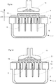
- the Fig. 1a - g show the parts involved in detaching and removing a semiconductor chip 1 from a film 3 of a mounting machine, namely a chip ejector 2 and a chip gripper 11, and the film 3 and the semiconductor chip 1 at successive times during the inventive picking process according to a first embodiment ,
- the parts involved are simplified and only shown insofar as this is necessary for the understanding of the picking process.
- the chip ejector 2 comprises a chamber 5, which can be acted upon by vacuum, with a replaceable cover with a bearing surface 13 on which the film 3 rests.
- the lid contains a plurality of holes 9 and 15.
- the diameter of the holes 9 is preferably only so large that the film 3 can not be drawn into the holes 9, ie the holes 9 are used essentially only to hold the film 3.
- needles 7 are arranged, which are usually displaceable perpendicular or obliquely to the support surface 13 of the lid.
- the distance is referred to the projecting their tips on the support surface 13.
- a negative z-value of the height means that the needles 7 are completely sunk in the holes 15 and therefore do not project beyond the support surface 13.
- the detachment and removal of the semiconductor chip 1 from the film 3 is extended according to the invention by a preparation phase, so that the entire process comprises three phases.
- the first phase is the preparation phase, in which the adhesive bond between the semiconductor chip 1 and the film 3 is weakened by means of the needles 7.
- the chip gripper 11 is not involved.
- the second phase is an immediately following phase, in which the chip gripper 11 supports the further detachment of the semiconductor chip 1 by the needles 7.
- the third phase of the chip gripper 11 is raised and moved away, wherein the semiconductor chip 1 completely detached from the film 3 without further support by the needles 7.
- the Fig. 1f shows a snapshot when the chip gripper 11 has already removed a piece of the film 3 with the recorded semiconductor chip 1. As shown, the needles 7 are only lowered below the support surface 13 when the chip gripper 11 has completely detached the semiconductor chip 1 from the film 3.
- the Fig. 1g shows a last snapshot after the needles 7 have been lowered back to a height z ⁇ 0, so that the picking process of the next semiconductor chip can be initiated. While the chip gripper 11 continues to process the semiconductor chip just removed, the first phase for the next semiconductor chip to be removed can already be started.
- the removal of the semiconductor chip 1 can be carried out in place of the method steps F to H described above with other steps that are adapted to the respective problem and as they are known from the prior art.
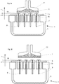
- the Fig. 2a - g show the parts involved in detaching and removing a semiconductor chip 1 from a film 3 of a mounting machine at successive times during the inventive picking process according to a second embodiment.
- the parts involved are simplified and only shown insofar as this is necessary for the understanding of the picking process.
- the chip ejector 2 in turn comprises the chamber 5, which can be acted upon by vacuum, with the lid with the bearing surface 13, on which the foil 3 rests.
- the support surface 13 includes an example rectangular opening 20 and a plurality of holes 9, which surround the opening 20 on at least three sides.
- In the opening 20 a parallel to the support surface 13 of the lid slidable carriage 21 is arranged.
- the displacement direction of the carriage 21 is referred to as x-direction. In the direction of displacement are:
- the length of the carriage about as large as the length of the semiconductor chip 1, the length of the opening 20 at least twice as large as the length of the semiconductor chip 1.
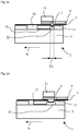
- Die Fig. 3 shows the chip ejector 2
- the detachment and removal of the semiconductor chip 1 from the film 3 in turn comprises a first, preparatory phase, in which the adhesive bond between the semiconductor chip 1 and the film 3 by means of the carriage 21, but without the participation of the chip gripper 11, is weakened.
- the second Phase is an immediately following phase, in which the chip gripper 11, the semiconductor chip 1 with support of the chip ejector 2 further separates from the film 3.
- the detachment of the semiconductor chip 1 from the film 3 can also with one of the devices of US 20050059205 be made, wherein the chip gripper is not involved in the first phase and wherein the chip ejector 2 in the second phase, the film 3 further detached from the semiconductor chip 1, while the semiconductor chip is held by the chip gripper 11, before in the third phase of the chip gripper 11th is lifted and moves away, taking with it the semiconductor chip 1.
- the described methods according to the invention are suitable both for semiconductor chips whose rear side is coated with an adhesive film and for comparatively large semiconductor chips whose edge lengths are greater than 10 mm and which are glued to the substrate with an adhesive applied to the substrate. Also in this case, the weakening of the adhesive bond in the first phase causes a shortening of the process time for the removal of the semiconductor chip, since the chip gripper has to help only for a very short time. Thanks to the invention, the detachment of the semiconductor chip from the film can already take place when the chip gripper is still busy with the bonding of the preceding semiconductor chip.
- the described embodiments contain only the most important steps. These steps may include further sub-steps or may be performed in a different order within the corresponding phase.
- the step of picking up an image of the semiconductor chip and determining its position or the deviation of its actual position from its desired position can also be carried out before the semiconductor chip is partially detached from the film, namely when its position in the other Replacement does not change anymore.
- the partial detachment of the semiconductor chip from the film can also be effected by other mechanical means than those described here.
Landscapes
- Container, Conveyance, Adherence, Positioning, Of Wafer (AREA)
Applications Claiming Priority (2)
| Application Number | Priority Date | Filing Date | Title |
|---|---|---|---|
| US11376108P | 2008-11-12 | 2008-11-12 | |
| PCT/EP2009/064535 WO2010054957A1 (de) | 2008-11-12 | 2009-11-03 | Verfahren zum ablösen und entnehmen eines halbleiterchips von einer folie |
Publications (2)
| Publication Number | Publication Date |
|---|---|
| EP2359398A1 EP2359398A1 (de) | 2011-08-24 |
| EP2359398B1 true EP2359398B1 (de) | 2017-05-10 |
Family
ID=41381913
Family Applications (1)
| Application Number | Title | Priority Date | Filing Date |
|---|---|---|---|
| EP09749087.4A Not-in-force EP2359398B1 (de) | 2008-11-12 | 2009-11-03 | Verfahren zum ablösen und entnehmen eines halbleiterchips von einer folie |
Country Status (8)
| Country | Link |
|---|---|
| US (1) | US8715457B2 (cg-RX-API-DMAC7.html) |
| EP (1) | EP2359398B1 (cg-RX-API-DMAC7.html) |
| JP (1) | JP2012508460A (cg-RX-API-DMAC7.html) |
| KR (1) | KR20110086698A (cg-RX-API-DMAC7.html) |
| CN (1) | CN102217052B (cg-RX-API-DMAC7.html) |
| MY (1) | MY155371A (cg-RX-API-DMAC7.html) |
| TW (1) | TWI543285B (cg-RX-API-DMAC7.html) |
| WO (1) | WO2010054957A1 (cg-RX-API-DMAC7.html) |
Families Citing this family (9)
| Publication number | Priority date | Publication date | Assignee | Title |
|---|---|---|---|---|
| KR101397750B1 (ko) * | 2012-07-25 | 2014-05-21 | 삼성전기주식회사 | 칩 이젝터 및 이를 이용한 칩 탈착 방법 |
| JP2019029650A (ja) * | 2017-07-26 | 2019-02-21 | 芝浦メカトロニクス株式会社 | 半導体チップのピックアップ装置、半導体チップの実装装置および実装方法 |
| CN107539596A (zh) * | 2017-09-29 | 2018-01-05 | 常熟市荣达电子有限责任公司 | 一种芯片包装盒及其操作方法 |
| JP7111816B2 (ja) * | 2018-07-30 | 2022-08-02 | アルバックテクノ株式会社 | 基板リフト装置及び基板搬送方法 |
| CH715447B1 (de) * | 2018-10-15 | 2022-01-14 | Besi Switzerland Ag | Chip-Auswerfer. |
| CN111341717B (zh) * | 2020-03-10 | 2023-02-07 | 长江存储科技有限责任公司 | 一种拾取装置和拾取方法 |
| US12394642B2 (en) * | 2021-07-30 | 2025-08-19 | Micraft System Plus Co., Ltd. | Apparatus for transferring electronic component, method for transferring electronic component and manufacturing method of light-emitting diode panel |
| JP7660459B2 (ja) * | 2021-08-05 | 2025-04-11 | 東京エレクトロン株式会社 | 接合装置および接合方法 |
| WO2026017270A1 (en) * | 2024-07-19 | 2026-01-22 | Nexperia B.V. | Apparatus and method for separating an electronics component from a flexible, adhesive film |
Family Cites Families (27)
| Publication number | Priority date | Publication date | Assignee | Title |
|---|---|---|---|---|
| JPS6415000A (en) * | 1987-07-09 | 1989-01-19 | Sumitomo Electric Industries | Chip packaging device |
| US4921564A (en) * | 1988-05-23 | 1990-05-01 | Semiconductor Equipment Corp. | Method and apparatus for removing circuit chips from wafer handling tape |
| JPH05283506A (ja) * | 1992-04-01 | 1993-10-29 | Sharp Corp | チップ突き上げ装置 |
| JP3498877B2 (ja) * | 1995-12-05 | 2004-02-23 | 株式会社東芝 | 半導体製造装置および半導体装置の製造方法 |
| JP3209736B2 (ja) * | 1999-11-09 | 2001-09-17 | エヌイーシーマシナリー株式会社 | ペレットピックアップ装置 |
| JP4482243B2 (ja) * | 2001-03-13 | 2010-06-16 | 株式会社新川 | ダイのピックアップ方法及びピックアップ装置 |
| KR20030046306A (ko) * | 2001-12-05 | 2003-06-12 | 에섹 트레이딩 에스에이 | 반도체 칩을 설치하기 위한 장치 |
| TWI225279B (en) * | 2002-03-11 | 2004-12-11 | Hitachi Ltd | Semiconductor device and its manufacturing method |
| AU2003249592A1 (en) * | 2002-07-17 | 2004-02-02 | Matsushita Electric Industrial Co., Ltd | Method and apparatus for picking up semiconductor chip and suction and exfoliation tool up therefor |
| EP1424722A1 (de) * | 2002-11-29 | 2004-06-02 | Esec Trading S.A. | Verfahren zum Aufnehmen von Halbleiterchips von einer Folie und Vorrichtung |
| TW200414992A (en) * | 2002-11-29 | 2004-08-16 | Esec Trading Sa | Method for picking semiconductor chips from a foil |
| JP4574251B2 (ja) * | 2003-09-17 | 2010-11-04 | ルネサスエレクトロニクス株式会社 | 半導体装置の製造方法 |
| EP1587138B1 (de) * | 2004-04-13 | 2007-05-30 | Oerlikon Assembly Equipment AG, Steinhausen | Einrichtung für die Montage von Halbleiterchips und Verfahren zum Ablösen eines Halbleiterchips von einer Folie |
| US7240422B2 (en) * | 2004-05-11 | 2007-07-10 | Asm Assembly Automation Ltd. | Apparatus for semiconductor chip detachment |
| CH697213A5 (de) | 2004-05-19 | 2008-06-25 | Alphasem Ag | Verfahren und Vorrichtung zum Ablösen eines auf eine flexible Folie geklebten Bauteils. |
| JP2006005030A (ja) | 2004-06-16 | 2006-01-05 | Matsushita Electric Ind Co Ltd | 半導体チップのピックアップ方法および装置 |
| US7238258B2 (en) * | 2005-04-22 | 2007-07-03 | Stats Chippac Ltd. | System for peeling semiconductor chips from tape |
| US20070158024A1 (en) * | 2006-01-11 | 2007-07-12 | Symbol Technologies, Inc. | Methods and systems for removing multiple die(s) from a surface |
| JPWO2008004270A1 (ja) * | 2006-07-03 | 2009-12-03 | キヤノンマシナリー株式会社 | ピックアップ方法およびピックアップ装置 |
| JP5283506B2 (ja) | 2006-09-12 | 2013-09-04 | 株式会社荏原製作所 | 研磨装置および研磨方法 |
| JP4755634B2 (ja) * | 2006-09-29 | 2011-08-24 | 東レエンジニアリング株式会社 | ピックアップ装置及びピックアップ方法 |
| US7665204B2 (en) * | 2006-10-16 | 2010-02-23 | Asm Assembly Automation Ltd. | Die detachment apparatus comprising pre-peeling structure |
| US8221583B2 (en) * | 2007-01-20 | 2012-07-17 | Stats Chippac Ltd. | System for peeling semiconductor chips from tape |
| JP4693805B2 (ja) * | 2007-03-16 | 2011-06-01 | 株式会社東芝 | 半導体装置の製造装置及び製造方法 |
| WO2009047214A2 (en) * | 2007-10-09 | 2009-04-16 | Oerlikon Assembly Equipment Ag, Steinhausen | Method for picking up semiconductor chips from a wafer table and mounting the removed semiconductor chips on a substrate |
| JP4985513B2 (ja) * | 2008-03-26 | 2012-07-25 | 富士通セミコンダクター株式会社 | 電子部品の剥離方法及び剥離装置 |
| CN102044404B (zh) * | 2009-10-12 | 2015-12-09 | 桑迪士克科技公司 | 用于使经切分的半导体裸片与裸片贴胶带分离的系统 |
-
2009
- 2009-11-03 EP EP09749087.4A patent/EP2359398B1/de not_active Not-in-force
- 2009-11-03 MY MYPI2011001736A patent/MY155371A/en unknown
- 2009-11-03 US US13/128,864 patent/US8715457B2/en active Active
- 2009-11-03 CN CN200980145287.4A patent/CN102217052B/zh active Active
- 2009-11-03 JP JP2011535096A patent/JP2012508460A/ja active Pending
- 2009-11-03 WO PCT/EP2009/064535 patent/WO2010054957A1/de not_active Ceased
- 2009-11-03 KR KR1020117010535A patent/KR20110086698A/ko not_active Ceased
- 2009-11-10 TW TW098138052A patent/TWI543285B/zh active
Also Published As
| Publication number | Publication date |
|---|---|
| CN102217052B (zh) | 2013-09-25 |
| CN102217052A (zh) | 2011-10-12 |
| WO2010054957A1 (de) | 2010-05-20 |
| JP2012508460A (ja) | 2012-04-05 |
| EP2359398A1 (de) | 2011-08-24 |
| MY155371A (en) | 2015-10-15 |
| KR20110086698A (ko) | 2011-07-29 |
| US8715457B2 (en) | 2014-05-06 |
| US20110214819A1 (en) | 2011-09-08 |
| TW201029093A (en) | 2010-08-01 |
| TWI543285B (zh) | 2016-07-21 |
Similar Documents
| Publication | Publication Date | Title |
|---|---|---|
| EP2359398B1 (de) | Verfahren zum ablösen und entnehmen eines halbleiterchips von einer folie | |
| EP2184765B1 (de) | Chip-Auswerfer | |
| DE60316575T2 (de) | Verfahren und vorrichtung zum aufnehmen von halbleiterchips sowie dazu verwendbares saugung ablöswerkzeug | |
| EP1587138B1 (de) | Einrichtung für die Montage von Halbleiterchips und Verfahren zum Ablösen eines Halbleiterchips von einer Folie | |
| AT506622B1 (de) | Vorrichtung und verfahren zum aufbringen und/oder ablösen eines wafers auf einen/von einem träger | |
| DE102012013370B4 (de) | Montagevorrichtung und Verfahren zum Fixieren einer Nadel in einem Nadelhalter einer Ausstoßvorrichtung zum Abheben eines Chips von einem Trägermaterial | |
| CH706280B1 (de) | Verfahren zum Ablösen eines Halbleiterchips von einer Folie. | |
| AT503848A2 (de) | Handhabungsvorrichtung sowie handhabungsverfahren für wafer | |
| DE102007063383B4 (de) | Vorrichtung und Verfahren zur Entfernung von Pelliclen von Masken | |
| EP2422357B1 (de) | Vorrichtung und verfahren zum trennen eines substrats von einem trägersubstrat | |
| CH697213A5 (de) | Verfahren und Vorrichtung zum Ablösen eines auf eine flexible Folie geklebten Bauteils. | |
| DE60317264T2 (de) | Verfahren zur Herstellung von Mikrohalbleiterbauelementen | |
| DE102018207498A1 (de) | Bearbeitungsverfahren für ein werkstück | |
| DE102006019709A1 (de) | Verfahren und Vorrichtung zum Zerschneiden von Wafern | |
| DE10146936B4 (de) | Herstellverfahren für eine Chipkomponenten-Baugruppe | |
| EP2490253B1 (de) | Vorrichtung und Verfahren zur Abnahme mindestens eines chipförmigen Halbleiterbauelements von einer Folie | |
| DE112006003158T5 (de) | Folienaufklebevorrichtung und Aufklebeverfahren | |
| DE10140827B4 (de) | Vorrichtung zum Debonden von Dünnwafern | |
| CH699851A1 (de) | Chip-Auswerfer und Verfahren zum Ablösen und Entnehmen eines Halbleiterchips von einer Folie. | |
| DE112006003839T5 (de) | Verfahren zur Herstellung eines dünnen Halbleiter-Chips | |
| DE102023201111A1 (de) | Wafertransferverfahren und wafertransfervorrichtung | |
| DE102008061165B4 (de) | Halbleiterbauelement mit einer Folie und Verfahren und Vorrichtung zum Herstellen eines solchen | |
| DE102009035099B4 (de) | Vorrichtung und Verfahren zum Abheben von Bauteilen von einem Träger | |
| EP3556567A1 (de) | Verfahren und vorrichtung zum aufbringen eines von einem streifenförmigen klebefilm separierten klebefilmabschnitts auf eine buchdecke | |
| DE2227324C3 (de) | Verfahren zum Abarbeiten der Einzelelemente einer eine Vielzahl von Halbleiteranordnungen enthaltenden Halbleiterscheibe und Vorrichtung zur Durchführung des Verfahrens |
Legal Events
| Date | Code | Title | Description |
|---|---|---|---|
| PUAI | Public reference made under article 153(3) epc to a published international application that has entered the european phase |
Free format text: ORIGINAL CODE: 0009012 |
|
| 17P | Request for examination filed |
Effective date: 20110614 |
|
| AK | Designated contracting states |
Kind code of ref document: A1 Designated state(s): AT BE BG CH CY CZ DE DK EE ES FI FR GB GR HR HU IE IS IT LI LT LU LV MC MK MT NL NO PL PT RO SE SI SK SM TR |
|
| DAX | Request for extension of the european patent (deleted) | ||
| 17Q | First examination report despatched |
Effective date: 20120430 |
|
| 17Q | First examination report despatched |
Effective date: 20120507 |
|
| GRAP | Despatch of communication of intention to grant a patent |
Free format text: ORIGINAL CODE: EPIDOSNIGR1 |
|
| STAA | Information on the status of an ep patent application or granted ep patent |
Free format text: STATUS: GRANT OF PATENT IS INTENDED |
|
| INTG | Intention to grant announced |
Effective date: 20170112 |
|
| GRAS | Grant fee paid |
Free format text: ORIGINAL CODE: EPIDOSNIGR3 |
|
| GRAA | (expected) grant |
Free format text: ORIGINAL CODE: 0009210 |
|
| STAA | Information on the status of an ep patent application or granted ep patent |
Free format text: STATUS: THE PATENT HAS BEEN GRANTED |
|
| RAP1 | Party data changed (applicant data changed or rights of an application transferred) |
Owner name: BESI SWITZERLAND AG |
|
| AK | Designated contracting states |
Kind code of ref document: B1 Designated state(s): AT BE BG CH CY CZ DE DK EE ES FI FR GB GR HR HU IE IS IT LI LT LU LV MC MK MT NL NO PL PT RO SE SI SK SM TR |
|
| REG | Reference to a national code |
Ref country code: GB Ref legal event code: FG4D Free format text: NOT ENGLISH |
|
| REG | Reference to a national code |
Ref country code: AT Ref legal event code: REF Ref document number: 893145 Country of ref document: AT Kind code of ref document: T Effective date: 20170515 Ref country code: CH Ref legal event code: EP |
|
| REG | Reference to a national code |
Ref country code: IE Ref legal event code: FG4D Free format text: LANGUAGE OF EP DOCUMENT: GERMAN |
|
| REG | Reference to a national code |
Ref country code: DE Ref legal event code: R096 Ref document number: 502009013960 Country of ref document: DE |
|
| REG | Reference to a national code |
Ref country code: NL Ref legal event code: MP Effective date: 20170510 |
|
| REG | Reference to a national code |
Ref country code: LT Ref legal event code: MG4D |
|
| PG25 | Lapsed in a contracting state [announced via postgrant information from national office to epo] |
Ref country code: HR Free format text: LAPSE BECAUSE OF FAILURE TO SUBMIT A TRANSLATION OF THE DESCRIPTION OR TO PAY THE FEE WITHIN THE PRESCRIBED TIME-LIMIT Effective date: 20170510 Ref country code: LT Free format text: LAPSE BECAUSE OF FAILURE TO SUBMIT A TRANSLATION OF THE DESCRIPTION OR TO PAY THE FEE WITHIN THE PRESCRIBED TIME-LIMIT Effective date: 20170510 Ref country code: FI Free format text: LAPSE BECAUSE OF FAILURE TO SUBMIT A TRANSLATION OF THE DESCRIPTION OR TO PAY THE FEE WITHIN THE PRESCRIBED TIME-LIMIT Effective date: 20170510 Ref country code: ES Free format text: LAPSE BECAUSE OF FAILURE TO SUBMIT A TRANSLATION OF THE DESCRIPTION OR TO PAY THE FEE WITHIN THE PRESCRIBED TIME-LIMIT Effective date: 20170510 Ref country code: NO Free format text: LAPSE BECAUSE OF FAILURE TO SUBMIT A TRANSLATION OF THE DESCRIPTION OR TO PAY THE FEE WITHIN THE PRESCRIBED TIME-LIMIT Effective date: 20170810 Ref country code: GR Free format text: LAPSE BECAUSE OF FAILURE TO SUBMIT A TRANSLATION OF THE DESCRIPTION OR TO PAY THE FEE WITHIN THE PRESCRIBED TIME-LIMIT Effective date: 20170811 |
|
| PG25 | Lapsed in a contracting state [announced via postgrant information from national office to epo] |
Ref country code: BG Free format text: LAPSE BECAUSE OF FAILURE TO SUBMIT A TRANSLATION OF THE DESCRIPTION OR TO PAY THE FEE WITHIN THE PRESCRIBED TIME-LIMIT Effective date: 20170810 Ref country code: IS Free format text: LAPSE BECAUSE OF FAILURE TO SUBMIT A TRANSLATION OF THE DESCRIPTION OR TO PAY THE FEE WITHIN THE PRESCRIBED TIME-LIMIT Effective date: 20170910 Ref country code: NL Free format text: LAPSE BECAUSE OF FAILURE TO SUBMIT A TRANSLATION OF THE DESCRIPTION OR TO PAY THE FEE WITHIN THE PRESCRIBED TIME-LIMIT Effective date: 20170510 Ref country code: PL Free format text: LAPSE BECAUSE OF FAILURE TO SUBMIT A TRANSLATION OF THE DESCRIPTION OR TO PAY THE FEE WITHIN THE PRESCRIBED TIME-LIMIT Effective date: 20170510 Ref country code: SE Free format text: LAPSE BECAUSE OF FAILURE TO SUBMIT A TRANSLATION OF THE DESCRIPTION OR TO PAY THE FEE WITHIN THE PRESCRIBED TIME-LIMIT Effective date: 20170510 Ref country code: LV Free format text: LAPSE BECAUSE OF FAILURE TO SUBMIT A TRANSLATION OF THE DESCRIPTION OR TO PAY THE FEE WITHIN THE PRESCRIBED TIME-LIMIT Effective date: 20170510 |
|
| PG25 | Lapsed in a contracting state [announced via postgrant information from national office to epo] |
Ref country code: DK Free format text: LAPSE BECAUSE OF FAILURE TO SUBMIT A TRANSLATION OF THE DESCRIPTION OR TO PAY THE FEE WITHIN THE PRESCRIBED TIME-LIMIT Effective date: 20170510 Ref country code: EE Free format text: LAPSE BECAUSE OF FAILURE TO SUBMIT A TRANSLATION OF THE DESCRIPTION OR TO PAY THE FEE WITHIN THE PRESCRIBED TIME-LIMIT Effective date: 20170510 Ref country code: RO Free format text: LAPSE BECAUSE OF FAILURE TO SUBMIT A TRANSLATION OF THE DESCRIPTION OR TO PAY THE FEE WITHIN THE PRESCRIBED TIME-LIMIT Effective date: 20170510 Ref country code: SK Free format text: LAPSE BECAUSE OF FAILURE TO SUBMIT A TRANSLATION OF THE DESCRIPTION OR TO PAY THE FEE WITHIN THE PRESCRIBED TIME-LIMIT Effective date: 20170510 Ref country code: CZ Free format text: LAPSE BECAUSE OF FAILURE TO SUBMIT A TRANSLATION OF THE DESCRIPTION OR TO PAY THE FEE WITHIN THE PRESCRIBED TIME-LIMIT Effective date: 20170510 |
|
| REG | Reference to a national code |
Ref country code: DE Ref legal event code: R097 Ref document number: 502009013960 Country of ref document: DE |
|
| PG25 | Lapsed in a contracting state [announced via postgrant information from national office to epo] |
Ref country code: IT Free format text: LAPSE BECAUSE OF FAILURE TO SUBMIT A TRANSLATION OF THE DESCRIPTION OR TO PAY THE FEE WITHIN THE PRESCRIBED TIME-LIMIT Effective date: 20170510 Ref country code: SM Free format text: LAPSE BECAUSE OF FAILURE TO SUBMIT A TRANSLATION OF THE DESCRIPTION OR TO PAY THE FEE WITHIN THE PRESCRIBED TIME-LIMIT Effective date: 20170510 |
|
| PLBE | No opposition filed within time limit |
Free format text: ORIGINAL CODE: 0009261 |
|
| STAA | Information on the status of an ep patent application or granted ep patent |
Free format text: STATUS: NO OPPOSITION FILED WITHIN TIME LIMIT |
|
| 26N | No opposition filed |
Effective date: 20180213 |
|
| PG25 | Lapsed in a contracting state [announced via postgrant information from national office to epo] |
Ref country code: SI Free format text: LAPSE BECAUSE OF FAILURE TO SUBMIT A TRANSLATION OF THE DESCRIPTION OR TO PAY THE FEE WITHIN THE PRESCRIBED TIME-LIMIT Effective date: 20170510 |
|
| PG25 | Lapsed in a contracting state [announced via postgrant information from national office to epo] |
Ref country code: MC Free format text: LAPSE BECAUSE OF FAILURE TO SUBMIT A TRANSLATION OF THE DESCRIPTION OR TO PAY THE FEE WITHIN THE PRESCRIBED TIME-LIMIT Effective date: 20170510 |
|
| GBPC | Gb: european patent ceased through non-payment of renewal fee |
Effective date: 20171103 |
|
| PG25 | Lapsed in a contracting state [announced via postgrant information from national office to epo] |
Ref country code: LI Free format text: LAPSE BECAUSE OF NON-PAYMENT OF DUE FEES Effective date: 20171130 Ref country code: CH Free format text: LAPSE BECAUSE OF NON-PAYMENT OF DUE FEES Effective date: 20171130 |
|
| PG25 | Lapsed in a contracting state [announced via postgrant information from national office to epo] |
Ref country code: LU Free format text: LAPSE BECAUSE OF NON-PAYMENT OF DUE FEES Effective date: 20171103 |
|
| REG | Reference to a national code |
Ref country code: FR Ref legal event code: ST Effective date: 20180731 Ref country code: BE Ref legal event code: MM Effective date: 20171130 |
|
| REG | Reference to a national code |
Ref country code: IE Ref legal event code: MM4A |
|
| PG25 | Lapsed in a contracting state [announced via postgrant information from national office to epo] |
Ref country code: MT Free format text: LAPSE BECAUSE OF FAILURE TO SUBMIT A TRANSLATION OF THE DESCRIPTION OR TO PAY THE FEE WITHIN THE PRESCRIBED TIME-LIMIT Effective date: 20170510 |
|
| PG25 | Lapsed in a contracting state [announced via postgrant information from national office to epo] |
Ref country code: IE Free format text: LAPSE BECAUSE OF NON-PAYMENT OF DUE FEES Effective date: 20171103 Ref country code: FR Free format text: LAPSE BECAUSE OF NON-PAYMENT OF DUE FEES Effective date: 20171130 |
|
| PG25 | Lapsed in a contracting state [announced via postgrant information from national office to epo] |
Ref country code: GB Free format text: LAPSE BECAUSE OF NON-PAYMENT OF DUE FEES Effective date: 20171103 Ref country code: BE Free format text: LAPSE BECAUSE OF NON-PAYMENT OF DUE FEES Effective date: 20171130 |
|
| REG | Reference to a national code |
Ref country code: AT Ref legal event code: MM01 Ref document number: 893145 Country of ref document: AT Kind code of ref document: T Effective date: 20171103 |
|
| PG25 | Lapsed in a contracting state [announced via postgrant information from national office to epo] |
Ref country code: AT Free format text: LAPSE BECAUSE OF NON-PAYMENT OF DUE FEES Effective date: 20171103 |
|
| PG25 | Lapsed in a contracting state [announced via postgrant information from national office to epo] |
Ref country code: HU Free format text: LAPSE BECAUSE OF FAILURE TO SUBMIT A TRANSLATION OF THE DESCRIPTION OR TO PAY THE FEE WITHIN THE PRESCRIBED TIME-LIMIT; INVALID AB INITIO Effective date: 20091103 |
|
| PG25 | Lapsed in a contracting state [announced via postgrant information from national office to epo] |
Ref country code: CY Free format text: LAPSE BECAUSE OF NON-PAYMENT OF DUE FEES Effective date: 20170510 |
|
| PG25 | Lapsed in a contracting state [announced via postgrant information from national office to epo] |
Ref country code: MK Free format text: LAPSE BECAUSE OF FAILURE TO SUBMIT A TRANSLATION OF THE DESCRIPTION OR TO PAY THE FEE WITHIN THE PRESCRIBED TIME-LIMIT Effective date: 20170510 |
|
| PG25 | Lapsed in a contracting state [announced via postgrant information from national office to epo] |
Ref country code: TR Free format text: LAPSE BECAUSE OF FAILURE TO SUBMIT A TRANSLATION OF THE DESCRIPTION OR TO PAY THE FEE WITHIN THE PRESCRIBED TIME-LIMIT Effective date: 20170510 |
|
| PG25 | Lapsed in a contracting state [announced via postgrant information from national office to epo] |
Ref country code: PT Free format text: LAPSE BECAUSE OF FAILURE TO SUBMIT A TRANSLATION OF THE DESCRIPTION OR TO PAY THE FEE WITHIN THE PRESCRIBED TIME-LIMIT Effective date: 20170510 |
|
| REG | Reference to a national code |
Ref country code: DE Ref legal event code: R081 Ref document number: 502009013960 Country of ref document: DE Owner name: BESI SWITZERLAND AG, CH Free format text: FORMER OWNER: BESI SWITZERLAND AG, CHAM, CH |
|
| PGFP | Annual fee paid to national office [announced via postgrant information from national office to epo] |
Ref country code: DE Payment date: 20241130 Year of fee payment: 16 |
|
| REG | Reference to a national code |
Ref country code: DE Ref legal event code: R119 Ref document number: 502009013960 Country of ref document: DE |
|
| PG25 | Lapsed in a contracting state [announced via postgrant information from national office to epo] |
Ref country code: DE Free format text: LAPSE BECAUSE OF NON-PAYMENT OF DUE FEES Effective date: 20250603 |