EP2354814B1 - Kapazitätssensor - Google Patents
Kapazitätssensor Download PDFInfo
- Publication number
- EP2354814B1 EP2354814B1 EP09830443.9A EP09830443A EP2354814B1 EP 2354814 B1 EP2354814 B1 EP 2354814B1 EP 09830443 A EP09830443 A EP 09830443A EP 2354814 B1 EP2354814 B1 EP 2354814B1
- Authority
- EP
- European Patent Office
- Prior art keywords
- terminal connecting
- connecting portion
- board
- terminal
- circuit
- Prior art date
- Legal status (The legal status is an assumption and is not a legal conclusion. Google has not performed a legal analysis and makes no representation as to the accuracy of the status listed.)
- Not-in-force
Links
Images


Classifications
-
- G—PHYSICS
- G01—MEASURING; TESTING
- G01B—MEASURING LENGTH, THICKNESS OR SIMILAR LINEAR DIMENSIONS; MEASURING ANGLES; MEASURING AREAS; MEASURING IRREGULARITIES OF SURFACES OR CONTOURS
- G01B7/00—Measuring arrangements characterised by the use of electric or magnetic techniques
-
- H—ELECTRICITY
- H03—ELECTRONIC CIRCUITRY
- H03K—PULSE TECHNIQUE
- H03K17/00—Electronic switching or gating, i.e. not by contact-making and –breaking
- H03K17/94—Electronic switching or gating, i.e. not by contact-making and –breaking characterised by the way in which the control signals are generated
- H03K17/945—Proximity switches
- H03K17/955—Proximity switches using a capacitive detector
-
- G—PHYSICS
- G01—MEASURING; TESTING
- G01V—GEOPHYSICS; GRAVITATIONAL MEASUREMENTS; DETECTING MASSES OR OBJECTS; TAGS
- G01V3/00—Electric or magnetic prospecting or detecting; Measuring magnetic field characteristics of the earth, e.g. declination, deviation
- G01V3/08—Electric or magnetic prospecting or detecting; Measuring magnetic field characteristics of the earth, e.g. declination, deviation operating with magnetic or electric fields produced or modified by objects or geological structures or by detecting devices
-
- H—ELECTRICITY
- H01—ELECTRIC ELEMENTS
- H01H—ELECTRIC SWITCHES; RELAYS; SELECTORS; EMERGENCY PROTECTIVE DEVICES
- H01H36/00—Switches actuated by change of magnetic field or of electric field, e.g. by change of relative position of magnet and switch, by shielding
-
- H—ELECTRICITY
- H01—ELECTRIC ELEMENTS
- H01R—ELECTRICALLY-CONDUCTIVE CONNECTIONS; STRUCTURAL ASSOCIATIONS OF A PLURALITY OF MUTUALLY-INSULATED ELECTRICAL CONNECTING ELEMENTS; COUPLING DEVICES; CURRENT COLLECTORS
- H01R13/00—Details of coupling devices of the kinds covered by groups H01R12/70 or H01R24/00 - H01R33/00
- H01R13/66—Structural association with built-in electrical component
- H01R13/665—Structural association with built-in electrical component with built-in electronic circuit
- H01R13/6683—Structural association with built-in electrical component with built-in electronic circuit with built-in sensor
-
- H—ELECTRICITY
- H05—ELECTRIC TECHNIQUES NOT OTHERWISE PROVIDED FOR
- H05K—PRINTED CIRCUITS; CASINGS OR CONSTRUCTIONAL DETAILS OF ELECTRIC APPARATUS; MANUFACTURE OF ASSEMBLAGES OF ELECTRICAL COMPONENTS
- H05K1/00—Printed circuits
- H05K1/02—Details
-
- H—ELECTRICITY
- H05—ELECTRIC TECHNIQUES NOT OTHERWISE PROVIDED FOR
- H05K—PRINTED CIRCUITS; CASINGS OR CONSTRUCTIONAL DETAILS OF ELECTRIC APPARATUS; MANUFACTURE OF ASSEMBLAGES OF ELECTRICAL COMPONENTS
- H05K1/00—Printed circuits
- H05K1/02—Details
- H05K1/11—Printed elements for providing electric connections to or between printed circuits
- H05K1/117—Pads along the edge of rigid circuit boards, e.g. for pluggable connectors
-
- H—ELECTRICITY
- H01—ELECTRIC ELEMENTS
- H01R—ELECTRICALLY-CONDUCTIVE CONNECTIONS; STRUCTURAL ASSOCIATIONS OF A PLURALITY OF MUTUALLY-INSULATED ELECTRICAL CONNECTING ELEMENTS; COUPLING DEVICES; CURRENT COLLECTORS
- H01R12/00—Structural associations of a plurality of mutually-insulated electrical connecting elements, specially adapted for printed circuits, e.g. printed circuit boards [PCB], flat or ribbon cables, or like generally planar structures, e.g. terminal strips, terminal blocks; Coupling devices specially adapted for printed circuits, flat or ribbon cables, or like generally planar structures; Terminals specially adapted for contact with, or insertion into, printed circuits, flat or ribbon cables, or like generally planar structures
- H01R12/50—Fixed connections
- H01R12/59—Fixed connections for flexible printed circuits, flat or ribbon cables or like structures
- H01R12/65—Fixed connections for flexible printed circuits, flat or ribbon cables or like structures characterised by the terminal
- H01R12/69—Fixed connections for flexible printed circuits, flat or ribbon cables or like structures characterised by the terminal deformable terminals, e.g. crimping terminals
-
- H—ELECTRICITY
- H03—ELECTRONIC CIRCUITRY
- H03K—PULSE TECHNIQUE
- H03K17/00—Electronic switching or gating, i.e. not by contact-making and –breaking
- H03K17/94—Electronic switching or gating, i.e. not by contact-making and –breaking characterised by the way in which the control signals are generated
- H03K17/96—Touch switches
- H03K2017/9602—Touch switches characterised by the type or shape of the sensing electrodes
-
- H—ELECTRICITY
- H03—ELECTRONIC CIRCUITRY
- H03K—PULSE TECHNIQUE
- H03K2217/00—Indexing scheme related to electronic switching or gating, i.e. not by contact-making or -breaking covered by H03K17/00
- H03K2217/94—Indexing scheme related to electronic switching or gating, i.e. not by contact-making or -breaking covered by H03K17/00 characterised by the way in which the control signal is generated
- H03K2217/94084—Transmission of parameters among sensors or between sensor and remote station
- H03K2217/94094—Wired transmission, e.g. via bus connection or similar
-
- H—ELECTRICITY
- H03—ELECTRONIC CIRCUITRY
- H03K—PULSE TECHNIQUE
- H03K2217/00—Indexing scheme related to electronic switching or gating, i.e. not by contact-making or -breaking covered by H03K17/00
- H03K2217/94—Indexing scheme related to electronic switching or gating, i.e. not by contact-making or -breaking covered by H03K17/00 characterised by the way in which the control signal is generated
- H03K2217/96—Touch switches
- H03K2217/9607—Capacitive touch switches
- H03K2217/960705—Safety of capacitive touch and proximity switches, e.g. increasing reliability, fail-safe
-
- H—ELECTRICITY
- H05—ELECTRIC TECHNIQUES NOT OTHERWISE PROVIDED FOR
- H05K—PRINTED CIRCUITS; CASINGS OR CONSTRUCTIONAL DETAILS OF ELECTRIC APPARATUS; MANUFACTURE OF ASSEMBLAGES OF ELECTRICAL COMPONENTS
- H05K1/00—Printed circuits
- H05K1/02—Details
- H05K1/11—Printed elements for providing electric connections to or between printed circuits
- H05K1/118—Printed elements for providing electric connections to or between printed circuits specially for flexible printed circuits, e.g. using folded portions
-
- H—ELECTRICITY
- H05—ELECTRIC TECHNIQUES NOT OTHERWISE PROVIDED FOR
- H05K—PRINTED CIRCUITS; CASINGS OR CONSTRUCTIONAL DETAILS OF ELECTRIC APPARATUS; MANUFACTURE OF ASSEMBLAGES OF ELECTRICAL COMPONENTS
- H05K2201/00—Indexing scheme relating to printed circuits covered by H05K1/00
- H05K2201/09—Shape and layout
- H05K2201/09209—Shape and layout details of conductors
- H05K2201/0929—Conductive planes
- H05K2201/09318—Core having one signal plane and one power plane
-
- H—ELECTRICITY
- H05—ELECTRIC TECHNIQUES NOT OTHERWISE PROVIDED FOR
- H05K—PRINTED CIRCUITS; CASINGS OR CONSTRUCTIONAL DETAILS OF ELECTRIC APPARATUS; MANUFACTURE OF ASSEMBLAGES OF ELECTRICAL COMPONENTS
- H05K2201/00—Indexing scheme relating to printed circuits covered by H05K1/00
- H05K2201/09—Shape and layout
- H05K2201/09209—Shape and layout details of conductors
- H05K2201/0929—Conductive planes
- H05K2201/09354—Ground conductor along edge of main surface
-
- H—ELECTRICITY
- H05—ELECTRIC TECHNIQUES NOT OTHERWISE PROVIDED FOR
- H05K—PRINTED CIRCUITS; CASINGS OR CONSTRUCTIONAL DETAILS OF ELECTRIC APPARATUS; MANUFACTURE OF ASSEMBLAGES OF ELECTRICAL COMPONENTS
- H05K2201/00—Indexing scheme relating to printed circuits covered by H05K1/00
- H05K2201/09—Shape and layout
- H05K2201/09209—Shape and layout details of conductors
- H05K2201/09654—Shape and layout details of conductors covering at least two types of conductors provided for in H05K2201/09218 - H05K2201/095
- H05K2201/09781—Dummy conductors, i.e. not used for normal transport of current; Dummy electrodes of components
-
- H—ELECTRICITY
- H05—ELECTRIC TECHNIQUES NOT OTHERWISE PROVIDED FOR
- H05K—PRINTED CIRCUITS; CASINGS OR CONSTRUCTIONAL DETAILS OF ELECTRIC APPARATUS; MANUFACTURE OF ASSEMBLAGES OF ELECTRICAL COMPONENTS
- H05K2201/00—Indexing scheme relating to printed circuits covered by H05K1/00
- H05K2201/10—Details of components or other objects attached to or integrated in a printed circuit board
- H05K2201/10007—Types of components
- H05K2201/10189—Non-printed connector
Definitions
- the present invention relates to an electrical capacitance sensor.
- Patent Document 1 Japanese Patent Application Publication No. 2007-139555 A capacitance sensor according to the preamble of claim 1 has been described in JP 2001 094408 A .
- the object of the present invention is to provide an electrical capacitance sensor having a small width size of the connecting section in spite of being provided with an electrode on the rear surface of a board.
- the present invention provides, for the purpose of solving the above problem, an electrical capacitance sensor comprising: a board having a one main surface and an other main surface; a sensor electrode formed on the one main surface of the board and detecting an electrical capacitance between the sensor electrode and an object; a first guard electrode formed on the one main surface of the board and in a vicinity of the sensor electrode; and a second guard electrode formed on the other main surface of the board, wherein a first terminal connecting portion for the first guard electrode and a second terminal connecting portion for the second guard electrode are provided at positions opposing each other.
- the electrical capacitance sensor further comprises: a third terminal connecting portion for the sensor electrode, the third terminal connecting portion being formed on the one main surface of the board; and a dummy terminal connecting portion formed at a position opposing the third terminal connecting portion and on the other main surface of the board, and the dummy terminal connecting portion may have a height approximately equal to a height of the second terminal connecting portion.
- a terminal clamp having a pair of clamping plates for clamping the board from both surface sides may be attached to each of a pair of the first terminal connecting portion and the second terminal connecting portion and a pair of the third terminal connecting portion and the dummy terminal connecting portion.
- the dummy terminal connecting portion may be formed of a conductive material same as for the second terminal connecting portion.
- a pair of the third terminal connecting portion and the dummy terminal connecting portion opposing each other may comprise a plurality of pairs of the third terminal connecting portions and the dummy terminal connecting portions, and the plurality of pairs may be arranged in substantially parallel to one another.
- the board may be provided as a membrane having an electrode section.
- the first terminal connecting portion for the first guard electrode provided on one main surface of the board and the second terminal connecting portion for the second guard electrode provided on the other main surface are located at positions opposing each other. Therefore, it is enabled that the width size of a connecting section including the first terminal connecting portion and the second terminal connecting portion does not become large even though the second guard electrode is formed on the other main surface of the board.
- the present invention provides an electrical capacitance sensor having a small connecting section while improving the detection accuracy thereof.
- an electrical capacitance sensor 100 according to embodiments of the present invention will be described with reference to the drawings. Hereinafter, the description will be directed illustratively to an embodiment in which the electrical capacitance sensor 100 according to the present embodiment is used as a sensor detecting a head position of an occupant seated at a vehicle seat.
- Figures 1 and 2 are views illustrating a headrest position adjusting apparatus 1000 to adjust a position of a headrest H in a vehicle in response to the head position of an occupant detected by the electrical capacitance sensor 100 according to the present embodiment.
- the headrest position adjusting apparatus 1000 shown in figures 1 and 2 has the electrical capacitance sensor 100, an in-vehicle computer such as ECU (Electronic Control Unit) 60, and a headrest forth and back driving motor 71 provided in the headrest H, and a headrest up and down driving motor 72 provided in a seat back S.
- ECU Electronic Control Unit
- the electrical capacitance sensor 100 has an electrode section 10 with a board arranged such that the main surface of the board is along the surface of the headrest H, and a sensor circuit 110 provided on another board different from the board of the electrode section 10.
- the electrode section 10 and the sensor circuit 110 are connected to each other via a connector.
- each sensor electrode 26 On one main surface side (front surface side) of the electrode section 10, five sensor electrodes 26 are formed so as to be arranged in substantially parallel to one another along the height direction of the headrest H. Each sensor electrode 26 independently detects an electrical capacitance and outputs each detected electrical capacitance to the sensor circuit 110.
- the sensor circuit 110 outputs a detecting signal depending on the obtained electrical capacitance to the ECU 60.
- the electrical capacitance sensor 100 is illustrated as being provided with five sensor electrodes 26 in the present embodiment, the number of the sensor electrodes 26 is not particularly limited.
- the ECU 60 controls the headrest forth and back driving motor 71 based on a distance, detected by the electrical capacitance sensor 100, between the surface of the headrest H and the head of occupant (distance between the sensor electrodes and the head of occupant).
- the headrest forth and back driving motor 71 moves the headrest H forth and back in accordance with a control instruction from the ECU 60.
- the calculation method of the distance between the surface of the headrest H and the head of occupant is not particularly limited. For example, the nearest distance out of the distances detected by the plurality of sensor electrodes 26 with different heights thereof may be determined as the distance between the surface of the headrest H and the head of occupant.
- the ECU 60 also controls the headrest up and down driving motor 72 based on a height of the occupant's head detected by the electrical capacitance sensor 100.
- the headrest up and down driving motor 72 moves the headrest H up and down in accordance with a control instruction from the ECU 60.
- the calculation method of the height of the occupant's head is not particularly limited.
- the height of the occupant's head can be obtained from an estimated result through detecting distances, each between the surface of the headrest H and the occupant's head, respectively by the plurality of the sensor electrodes 26 arranged in substantially parallel to one another along the height direction of the headrest H, determining which sensor electrode 26 is detecting the nearest distance, and estimating the height of the occupant's head in accordance with the height position of the determined sensor electrode 26.
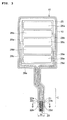
- Figure 3 is a plan view of a board 10 on which electrodes of the electrical capacitance sensor according to the present embodiment are formed
- figure 4 is a rear view thereof
- figure 5 is a cross sectional view along the line V-V in figure 3 .
- sensor electrodes 26a to 26e formed on one main surface of the board are sensor electrodes 26a to 26e each for detecting an electrical capacitance between each sensor electrode and an object, and a first guard electrode 25 formed in the vicinity of the sensor electrodes 26a to 26e, more specifically formed around the sensor electrodes 26a to 26e.
- the sensor electrodes 26a to 26e are connected with third terminal connecting portions 22a to 22e respectively via connecting wirings 28a to 28e, and the first guard electrode 25 is connected with a first terminal connecting portion 21 via a connecting wiring 25a.
- an additional first guard electrode 25 may be provided on an upper layer of a laminated board configured as the board 10 such that the additional first guard electrode 25 is located via an insulating layer above the connecting wirings 28a to 28e connected with the sensor electrodes 26a to 26e.
- the first terminal connecting portion 21 may be common for the two first guard electrodes 25 by providing a contact therebetween at a certain position of the first guard electrode 25 shown in figure 3 .
- a second guard electrode 27 is formed on the other main surface (rear surface) of the board 10.
- the second guard electrode 27 is connected with a second terminal connecting portion 23 via a connecting wiring 27a.
- five dummy terminal connecting portions 24a to 24e are provided in parallel to one another and adjacently to and parallelly to the second terminal connecting portion 23.
- essential parts constituting a connecting section 20 are the first terminal connecting portion 21 and the third terminal connecting portions 22a to 22e provided on the one main surface side of the board 10 and the second terminal connecting portion 23 and the dummy terminal connecting portions 24a to 24e provided on the other main surface side of the board.
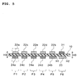
- Figure 5 which is a cross sectional view along the line V-V in figure 3 , illustrates a cross section of the connecting section 20 including the first terminal connecting portion 21, the second terminal connecting portion 23, the third terminal connecting portions 22a to 22e, and the dummy terminal connecting portions 24a to 24e.
- the first terminal connecting portion 21 for the first guard electrode 25 and the second terminal connecting portion 23 for the second guard electrode 27 are provided at positions opposing each other on both main surfaces of the board 10.
- the first guard electrode 25 and the second guard electrode 27 are provided respectively on the one main surface and the other main surface of the board 10. Therefore, both the guard electrodes 25 and 27 are to be applied same voltage and to perform similarly in spite of being provided on which surface of the board 10.
- features of the present embodiment include that the first terminal connecting portion 21 for the first guard electrode 25 and the second terminal connecting portion 23 for the second guard electrode 27, which have same performances, are provided at positions opposing each other on both main surfaces of the board 10, that a single terminal clamp is attached to the pair of terminal connecting portions (terminal connecting portion pair P6) opposing each other, and that a certain voltage is applied to these terminal connecting portions.
- the width size W (refer to figure 3 ) of the connecting section 20 including the first terminal connecting portion 21 and the second terminal connecting portion 23 is prevented from becoming large, and it is enabled to reduce the width size W of the connecting section 20.
- the dummy terminal connecting portions 24a to 24e are provided on the other main surface side of the board 10 and at positions opposing respectively the third terminal connecting portions 22a to 22e.
- each of the third terminal connecting portions 22a to 22e provided on the one main surface side of the board 10 becomes paired together with each of the dummy terminal connecting portions 24a to 24e provided on the other main surface side of the board 10, and therefore five terminal connecting portion pairs P1 to P5 each being counterparts are arranged in substantially parallel to one another.
- Each dummy terminal connecting portion 24 is formed to have the height (thickness) H1 thereof approximately equal to the height (thickness) H2 of the second terminal connecting portion 23. Accordingly, the heights H1 and H2 on the other main surface side of the connecting section 20 can be obtained evenly. As a result, the height H3 of a connecting region C ( figures 3 and 4 ) may become uniformly even. Thus, in the connecting region C, the height H3 of the terminal connecting portion pair P6 comprising the first terminal connecting portion 21 and the second terminal connecting portion 23 becomes even with the heights H3 of the terminal connecting portion pairs P1 to P5 comprising the third terminal connecting portions 22a to 22e and the dummy terminal connecting portions 24a to 24e.
- each terminal connecting portion pair is electrically conducted by using each terminal clamp 5 such that a pair of clamping plates provided with the terminal clamp 5 holds the terminal connecting portion pair therebetween from both main surface sides of the board 10, the variation of connecting conditions (pressing forces and the like) is suppressed, thereby improving a connecting reliability.
- the connecting section 20 which includes the terminal connecting portion pair P6 comprising the first terminal connecting portion 21 and the second terminal connecting portion 23 and the terminal connecting portion pairs P1 to P5 comprising the third terminal connecting portions 22a to 22e and the dummy terminal connecting portions 24a to 24e, is electrically connected with the sensor circuit 110 shown in figure 2 in such a manner that the pair of clamping plates provided with each of six terminal clamps 5 to be described later holds each terminal connecting portion pair therebetween from both main surface sides of the board 10.
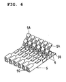
- FIGS 6 to 8 the terminal clamps 5 and a connector 200 provided therein with the terminal clamps 5 according to the present embodiment will be described.
- Figures 6 and 7 are perspective views each illustrating the terminal clamps 5, and figure 8 is an exploded perspective view illustrating the connector 200 including the terminal clamps 5.
- each of the terminal clamps 5 is configured of an electrically conductive material and is provided with a pair of clamping plates 5A and 5B for holding the board 10 not shown in figure 6 .
- the clamping plate 5B has barrels 6 (hooks 6) capable of being swaged into barrel shapes.
- Each terminal clamp 5 has an insertion opening 5C formed at one end side thereof into which a male terminal is to be inserted.
- six terminal connecting portion pairs P1 to P6 are provided with certain intervals according to the present embodiment, and therefore six terminal clamps 5 are provided with the certain intervals.
- Figure 7 illustrates the terminal clamps 5 in a condition where the barrels 6 have been swaged by using a jig or a tool not shown. As shown in figure 7 , six terminal clamps 5 are fixed to the connecting section 20 of the board 10 with intervals corresponding to the certain intervals of the terminal connecting portion pairs P1 to P6.
- the clamping plates 5A and 5B are fixed to each of the terminal connecting portion pairs P1 to P6 through the following steps: a step where the terminal clamps 5 are set such that each of the terminal connecting portion pairs P1 to P6 is located between each pair of the clamping plates 5A and 5B; a step where the tops of the barrels 6 projecting from each clamping plate 5B are passed through openings 3 provided at the board 10; a step where each of the terminal connecting portion pairs P1 to P6 are clamped between the each pair of the clamping plates 5A and 5B; and a step where the barrels 6 are swaged such that the clamping plates 5A and 5B are pressed towards the board 10 from both main surface sides thereof.
- the connecting section 20 which includes the terminal connecting portion pair P6 comprising the first terminal connecting portion 21 and the second terminal connecting portion 23 and the terminal connecting portion pairs P1 to P5 comprising the third terminal connecting portions 22 and the dummy terminal connecting portions 24, is fixed to the terminal clamps 5 so as to be clamped respective clamping plates 5A and 5B.
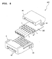
- Figure 8 is an exploded perspective view illustrating a situation where the terminal connecting portion pairs P1 to P6 and the terminal clamps 5 are placed in a connector housing 9 after being connected with one another.
- the connector housing 9 has an engaging projection 94 to be engaged into an engaging opening 93 of a cover 92 provided with the connector housing 9, and the positions of the terminal clamps 5 are determined after the engaging opening 93 being engaged with the engaging projection 94.
- terminal plugs of the counterpart connector connected with the sensor circuit 110 shown in figure 2 are inserted into six openings 95 of the connector housing 9, thereby the sensor electrodes 26a to 26e, the first guard electrode 25, and the second guard electrode 27 are electrically connected to the sensor circuit 110.
- the electrical capacitance sensor 100 is a sensor having an electrode section with a board of membrane. More specifically, the electrode section is obtained by forming electrodes and wirings through a printing method on the surface of an insulating base material with flexibility.
- an insulating base material for constituting the board 10 is prepared.
- a resin material may be used as the insulating base material because of having significant flexibility. Examples thereof include resin films such as polyimide-based film, polyamide-based resin film, polyethylene terephthalate film, and polyethylene naphthalate film.
- the conductive paste include paste obtained by dispersing conductive filler of metal powder, such as silver, platinum, gold, copper, nickel, and palladium, into binder resin. It is to be noted that the printing method of the conductive paste is not particularly limited, and a method known in the art is available.
- the second guard electrode 27, the connecting wiring 27a, the second terminal connecting portion 23, and the dummy terminal connecting portions 24 are formed on the insulating base material. Same manner as for the sensor electrodes 26 and the like is available as the printing method.
- the dummy terminal connecting portions 24 are formed of the same conductive materials as for the second terminal connecting portion 23. Therefore, the second terminal connecting portion 23 and the dummy terminal connecting portions 24a to 24e can be formed through a single printing process. Thus, a particular process for providing the dummy terminal connecting portions 24a to 24e is unnecessary because the second terminal connecting portion 23 and the dummy terminal connecting portions 24a to 24e are simultaneously formed.
- the electrical capacitance sensor 100 has a configuration where the first terminal connecting portion 21 for the first guard electrode 25 formed on one main surface of the board 10 and the second terminal connecting portion 23 for the second guard electrode 27 formed on the other main surface of the board 10 are arranged so as to oppose each other. Therefore, both the first terminal connecting portion 21 and the second terminal connecting portion 23 can be connected with one terminal clamp 5.
- the electrical capacitance sensor 100 is configured such that the first terminal connecting portion 21 and the second terminal connecting portion 23 are arranged to be opposed each other. Therefore, in the case of forming the second guard electrode 27 on the other main surface of the board 10 as the above embodiment, it is unnecessary to ensure an additional region to be assigned to the second terminal connecting portion 23 for the second guard electrode 27. Accordingly, the width size W (refer to figure 3 ) of the connecting section 20, to which the terminal clamps 5 are fixed, is prevented from increasing, thereby providing the electrical capacitance sensor 100 with a small width size W of the connecting section 20.
- the number of the terminal clamps 5 to be connected with the connecting section 20 is common for the cases that the guard electrodes 25 and 27 are provided on both main surfaces of the board 10 and that the guard electrode 25 is provided only on one main surface of the board 10, connectors according to common specs are available for connecting sections 20 of these cases.
- the electrode section 10 is arranged so as to be along the front surface of the headrest H, and the sensor circuit 110 is located at the rear side of the headrest H. Therefore, it is required that a penetrating hole is formed in a cushion material (sponge) of the headrest H in order for the connector 200 of the board 10 to pass through from the front surface side to the rear surface side of the headrest H. Because the size of the penetrating hole is determined in accordance with the width size of the connector 200, the penetrating hole becomes large as the connector 200 becomes large. If the penetration hole is large, the occupant contacting with the headrest H may be bothered by a feeling of strangeness. Accordingly, it is desired to reduce sizes of the terminal clamps 5 and the connector 200.
- the headrest H with high performances are developed through providing functions of adjusting right and left position, up and down position and the like in addition to the adjustment of forth and back position, it is anticipated that the number of the sensor electrodes 26 used in the electrical capacitance sensor 100 increases. Also in this case, it is highly expected to suppress the increase of the number of the terminal clamps 5 to be connected with the terminal connecting portions and to reduce the size of the connector 200.
- the electrical capacitance sensor 100 has futures including that the number of the terminal clamps 5 to be connected with the terminal connecting portions in the connecting section 20 is suppressed thereby reducing the size of the connector 200.
- the second guard electrode 27 on the other main surface. Therefore, it is enabled to heighten the detection accuracy while trying to reduce the size of the connecting section 20.
- the presence of metal members such as shafts supporting the headrest H may cause to deteriorate the detection accuracy in the case of providing the electrode section 10 of the electrical capacitance sensor such that the main surface of the board is along the surface of the headrest H. In such a case, it is possible to maintain the high detection accuracy by forming the second guard electrode 27 on the other main surface of the board.
- the plurality of the third terminal connecting portions 22a to 22e and the plurality of the dummy terminal connecting portions 24a to 24e are arranged to oppose one another, thereby forming the plurality of the terminal connecting portion pairs P1 to P5.
- the terminal connecting portion pairs P1 to P6 can be clamped at the same time by the terminal clamps 5 in the same condition as for the terminal connecting portion pair P6 of the first terminal connecting portion 21 and the second terminal connecting portion 23. Therefore, it is enabled to provide a simple production process compared with the case of clamping pair-by-pair the terminal portion pairs.
- the first terminal connecting portion 21, the second terminal connecting portion 23, the third terminal connecting portions 22, and the dummy terminal connecting portions 24 can be clamped at one time operation to form a connector, it is enabled to obtain uniform connecting conditions for the terminal connecting portions. As a result, the connection reliability can be improved through suppressing the variability in connecting conditions of the terminal connecting portions.
- clamping is used as a method of electrical connection for the first terminal connecting portion 21, second terminal connecting portion 23, the third terminal connecting portions 22, and the dummy terminal connecting portions 24 formed on the board 10. Therefore, electrodes on one main surface can be conducted to electrodes on the other main surface without forming through-holes and the like, and a simple production process can be obtained.
- the heights (thicknesses) H1 of the dummy terminal connecting portions 24 are approximately equal to the height (thickness) H2 of the second terminal connecting portion 23, uniform heights H3 can be obtained within the connecting section 20 of the board 10 to be clamped by the terminal clamps 5. Therefore, uniform pressing forces are given by the terminal clamps 5 clamping the terminal connecting portions 21, 22, 23, and 24, and the connection reliability can be improved through suppressing the variability in connecting conditions of the terminals.
- the electrical capacitance sensor 100 is a sensor having an electrode section with a board of membrane, in which the electrode section is obtained by forming electrodes and wirings through a printing method on the surface of an insulating base material with flexibility, it may be hard to form through-holes as means for conducting both main surfaces of the board 10.
- the first terminal connecting portion 21 and the second terminal connecting portion 23 formed on both main surfaces of the board 10 can be conducted by means of the terminal clamp 5.
- circuit conducting structures according to the second embodiment will be described.
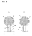
- Figures 9(A) and 9(B) are views illustrating a circuit board according to the present embodiment.
- figure 9(A) is a view illustrating the front surface side of the circuit board according to the present embodiment
- figure 9(B) is a view illustrating the rear surface side of the circuit board according to the present embodiment.
- a sensor electrode 26 As shown in figure 9(A) , formed on the front surface of the circuit board 10 are a sensor electrode 26, a first guard electrode 25 arranged around the sensor electrode 26, a third circuit 22 having an end connected with the sensor electrode 26, and a first circuit 21 having an end connected with the first guard electrode 25. Also as shown in figure 9(B) , formed on the rear surface of the circuit board 10 are a second guard electrode 27 and a second circuit 23 having an end connected with the second guard electrode 27.
- the circuit board 10 is, for example, a flexible circuit board obtained by providing the sensor electrode 26, the first guard electrode 25, the second guard electrode 27, and the first to third circuits 21, 23, and 22 each formed of copper (Cu) foil onto an insulating base material configured of a resin sheet of polyimide, polyethylene naphthalate, polyethylene terephthalate, or the like.
- the first circuit 21 has one end connected with the first guard electrode 25 and the other end reaching an end portion 11 of the circuit board
- the third circuit 22 has one end connected with the sensor electrode 26 and the other end reaching the end portion 11 of the circuit board.
- the second circuit 23 has one end connected with the second guard electrode 27 and the other end reaching the end portion 11 of the circuit board.
- the circuit end of the first circuit 21 and the circuit end of the second circuit 23 are located at positions on the front and the rear surfaces of the circuit board opposing each other. Also regarding the end portion 11 of the circuit board, a dummy circuit 24 is provided such that the circuit end of the third circuit 22 and the dummy circuit 24 are located at positions on the front and the rear surfaces of the circuit board opposing each other.
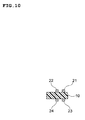
- Figure 10 is an enlarged sectional view of the circuit board according to the present embodiment along the line A-A in figure 9(A) .
- the end portion of the second circuit 23 is elongated on the opposing surface corresponding via the circuit board 10 to the end portion of the first circuit 21 elongated to the end portion 11 of the circuit board 10, and the dummy circuit 24 is arranged on the opposing surface corresponding via the circuit board 10 to the end portion of the third circuit 22.
- connections for two circuits 21 and 23 can be achieved at one time through using a both-sided connecting terminal capable of connecting two circuits provided on both surfaces of the board with another circuit by clamping in up-and-down direction.
- connections for the circuit 22 and the dummy circuit 24 can be achieved by using a both-sided connecting terminal capable of connecting two circuits with another circuit by clamping in up-and-down direction.
- FIGS. 11(A) and 11(B) are schematic views illustrating the connecting structure according to the present embodiment.
- figure 11(A) is a view illustrating the front surface side of the circuit board to which the connecting structure according to the present embodiment is applied
- figure 11 (B) is a view illustrating the rear surface side of the circuit board to which the connecting structure according to the present embodiment is applied.
- the first to the third circuits 21, 23, and 22 are respectively elongated to the end portion 11 of the circuit board 10 and connected to wires 41 and 42 by means of both-sided connecting terminals 31 and 32.
- end portion 11 the both-sided connecting terminals 31 and 32, and the circuit board 10 side end portions of the wires 41 and 42 are molded by a hot melt mold 50.
- the end portion of the first circuit 21 connected with the first guard electrode 25 and the end portion of the second circuit 23 connected with the second guard electrode 27 are clamped by the both-sided connecting terminal 31 in up-and-down direction, thereby being connected with the wire 41.
- a guard voltage may be applied to the wire 41 connected with the first and the second circuits 21 and 23. In this case, it is unnecessary to apply the guard voltage independently to each of the first and the second circuits 21 and 23 through a wire.
- the third circuit 22 can be connected with the wire 42 by using the both-sided connecting terminal 32 to clamp the third circuit 22 and the dummy circuit 24 in up-and-down direction under the same pressure bonding condition as for a circuit end pair comprising the circuit ends of the first circuit 21 and the second circuit23.
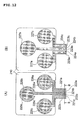
- Figures 12(A) and 12(B) are views illustrating a circuit board for multi channel electrical capacitance sensor.
- figure 12(A) is a view illustrating the front surface side of the circuit board for multi channel electrical capacitance sensor
- figure 12(B) is a view illustrating the rear surface side of the circuit board for multi channel electrical capacitance sensor.
- the circuit board 210 formed on the front surface of the circuit board 210 are three sensor electrodes 226a to 226c, three first guard electrodes 225a to 225c arranged respectively around the sensor electrodes 226a to 226c, three third circuits 222a to 222c having ends connected respectively with the sensor electrodes 226a to 226c, and three first circuits 221a to 221c having ends connected respectively with the first guard electrodes 225a to 225c.
- the rear surface of the circuit board 210 formed on the rear surface of the circuit board 210 are three second guard electrodes 227a to 227c and three second circuits 223a to 223c having ends connected respectively with the second guard electrodes 227a to 227c.
- the circuit board 210 is, similarly as the above embodiment, a flexible circuit board obtained by providing the sensor electrodes 226a to 226c, the first guard electrodes 225a to 225c, the second guard electrodes 227a to 227c, and the first to third circuits 221a to 221c, 223a to 223c, and 222a to 222c each formed of copper (Cu) foil onto an insulating base material configured of an insulating sheet of polyimide, polyethylene naphthalate, polyethylene terephthalate, or the like.
- Cu copper
- the three first circuits 221a to 221c have one ends connected respectively with the first guard electrodes 225a to 225c and the other ends reaching an end portion 211 of the circuit board, and the three third circuits 222a to 222c have one ends connected respectively with the sensor electrodes 226a to 226c and the other ends reaching the end portion 211 of the circuit board.
- the three second circuits 223a to 223c have one ends connected respectively with the second guard electrodes 227a to 227c and the other ends reaching the end portion 211 of the circuit board.
- the circuit ends of the three first circuits 221a to 221c and the circuit ends of the three second circuits 223a to 223c are located at positions on the front and the rear surfaces of the circuit board opposing one another.
- three dummy circuits 224a to 224c are provided such that the circuit ends of the three third circuits 222a to 222c and the dummy circuits 224a to 224c are located respectively at positions on the front and the rear surfaces of the circuit board opposing one another.
- Figure 13 is an enlarged sectional view of the circuit board for the multi channel electrical capacitance sensor along the line B-B in figure 12(A) .
- the end portions of the second circuits 223a to 223c are elongated on the opposing surface corresponding via the circuit board 210 to the end portions of the first circuits 221 a to 221c elongated to the end portion 211 of the circuit board 210, and the dummy circuits 224a to 224c are arranged on the opposing surface corresponding via the circuit board 210 to the end portions of the third circuits 222a to 222c.
- connections for respective two circuits of the first circuits 221a to 221c and the second circuits 223a to 223c can be achieved at one time through using both-sided connecting terminals each capable of connecting two circuits provided on both surfaces of the board with another circuit by clamping in up-and-down direction.
- connections for the third circuits 222a to 222c and the dummy circuits 224a to 224c can be achieved by using both-sided connecting terminals each capable of connecting two circuits with another circuit by clamping in up-and-down direction.
- circuit end pairs are formed on the end portion 211 of the circuit board 210, and the both-sided connecting terminal is to be attached to each circuit end pair. If the dummy circuits 224a to 224c are absent, differences in thicknesses among the circuit end pairs may occur when trying to attach six both-sided connecting terminals to the circuit end pairs at one time, thereby deteriorating the reliability of the connection between each both-sided connecting terminal and each circuit.
- the differences in thicknesses among the circuit end pairs are prevented from occurring because the dummy circuits 224a to 224c are provided. Therefore, it is enabled to press bond the circuit end pairs of the third circuits 222a to 222c and the dummy circuits 224a to 224c under the same press bonding condition as for the circuit end pairs of the circuits 221a to 221c and the second circuits 223a to 223c.
- the flexible circuit board should be understood as including a membrane obtained by printing silver paste as electrodes and circuits onto an insulating base material of insulating film formed of polyethylene naphthalate, polyethylene terephthalate, or the like.
Claims (5)
- Elektrischer Kapazitätssensor (100) mit:einer Platine (10), die eine Hauptfläche und eine andere Hauptfläche aufweist,einer Sensorelektrode (26a-e), die auf der einen Hauptfläche der Platine (10) gebildet ist und eine elektrische Kapazität zwischen der Sensorelektrode und einem Objekt detektiert,einer ersten Schutzelektrode (25), die auf der einen Hauptfläche der Platine (10) und in der Nachbarschaft der ersten Sensorelektrode (26a-e) angeordnet ist,einer zweiten Schutzelektrode (27), die auf der anderen Hauptfläche der Platine (10) gebildet ist,wobei ein erster Klemmenanschlussteil (21) für die erste Schutzelektrode (25) und ein zweiter Klemmenanschlussteil (23) für die zweite Schutzelektrode (27) in einander gegenüberliegenden Positionen angeordnet sind,wobei der Kapazitätssensor weiterhin aufweist:einen dritten Klemmenanschlussteil (22a-e) für die Sensorelektrode, welcher dritte Klemmenanschlussteil auf der einen Hauptfläche der Platine (10) gebildet ist, gekennzeichnet durch:einen Blindklemmenanschlussteil (24a-e), der in einer Position gegenüberliegend zu dem dritten Klemmenanschlussteil (22a-22e) und auf der anderen Hauptfläche der Platine (10) gebildet ist,wobei der Blindklemmenanschlussteil (24a-e) eine Höhe hat, die annähernd gleich der Höhe des zweiten Klemmenanschlussteils (22a-e) ist.
- Elektrischer Kapazitätssensor nach Anspruch 1, bei dem
eine Anschlussklemme (5), die zwei Klemmplatten zum Klemmen der Platine von beiden Seiten her aufweist, sowohl an einem durch den ersten Klemmenanschlussteil (21) und den zweiten Klemmenanschlussteil (23) gebildeten Paar als auch an einem durch den dritten Klemmenanschlussteil (22a-e) und dem Blindklemmenanschlussteil (24a-e) gebildeten Paar angebracht ist. - Elektrischer Kapazitätssensor nach Anspruch 1, bei dem
der Blindklemmenanschlussteil (24a-e) aus dem gleichen leitfähigen Material gebildet ist wie der zweite Klemmenanschlussteil (23). - Elektrischer Kapazitätssensor nach Anspruch 1, bei dem
ein durch den dritten Klemmenanschlussteil (22a-e) und den Blindklemmenanschlussteil (24a-e), die einander gegenüberliegen, gebildetes Paar mehrere Paare der dritten Klemmenanschlussteile und der Blindklemmenanschlussteile aufweist und die mehreren Paare im wesentlichen parallel zueinander angeordnet sind. - Elektrischer Kapazitätssensor nach Anspruch 1, bei dem die Platine (10) als eine Membran mit einem Elektrodenteil ausgebildet ist.
Applications Claiming Priority (2)
| Application Number | Priority Date | Filing Date | Title |
|---|---|---|---|
| JP2008309408 | 2008-12-04 | ||
| PCT/JP2009/070297 WO2010064677A1 (ja) | 2008-12-04 | 2009-12-03 | 静電容量センサ |
Publications (3)
| Publication Number | Publication Date |
|---|---|
| EP2354814A1 EP2354814A1 (de) | 2011-08-10 |
| EP2354814A4 EP2354814A4 (de) | 2013-10-09 |
| EP2354814B1 true EP2354814B1 (de) | 2014-10-08 |
Family
ID=42233324
Family Applications (1)
| Application Number | Title | Priority Date | Filing Date |
|---|---|---|---|
| EP09830443.9A Not-in-force EP2354814B1 (de) | 2008-12-04 | 2009-12-03 | Kapazitätssensor |
Country Status (6)
| Country | Link |
|---|---|
| US (1) | US8487638B2 (de) |
| EP (1) | EP2354814B1 (de) |
| JP (1) | JP5161320B2 (de) |
| KR (1) | KR101248127B1 (de) |
| CN (1) | CN102124305B (de) |
| WO (1) | WO2010064677A1 (de) |
Families Citing this family (14)
| Publication number | Priority date | Publication date | Assignee | Title |
|---|---|---|---|---|
| US20130342189A1 (en) * | 2010-09-06 | 2013-12-26 | Cummins Ltd. | Rotational device |
| JP5353991B2 (ja) * | 2010-11-30 | 2013-11-27 | 株式会社日本自動車部品総合研究所 | 静電容量式乗員検知装置 |
| DE102011078077A1 (de) * | 2011-06-24 | 2012-12-27 | Ident Technology Ag | Leiterplatte mit Elektrodenkonfiguration eines kapazitiven Sensors |
| JP5838408B2 (ja) * | 2011-10-27 | 2016-01-06 | 株式会社生方製作所 | 静電容量式液面センサー |
| US8981602B2 (en) * | 2012-05-29 | 2015-03-17 | Ford Global Technologies, Llc | Proximity switch assembly having non-switch contact and method |
| JP6028479B2 (ja) * | 2012-09-14 | 2016-11-16 | オムロン株式会社 | 静電容量型センサ、音響センサ及びマイクロフォン |
| JP6020745B2 (ja) * | 2014-04-07 | 2016-11-02 | 株式会社村田製作所 | タッチセンサ |
| JP6645978B2 (ja) * | 2014-10-22 | 2020-02-14 | バンドー化学株式会社 | 静電容量型センサ |
| DE102015205560A1 (de) * | 2015-03-26 | 2016-09-29 | Conti Temic Microelectronic Gmbh | Vorrichtung zur Erkennung der Anwesenheit und/oder Bewegungsrichtung von Objekten im Nahbereich mittels eines elektrischen Felds |
| DE102015212166A1 (de) * | 2015-06-30 | 2017-01-05 | Robert Bosch Gmbh | Ortungsvorrichtung |
| US10571423B2 (en) | 2016-06-24 | 2020-02-25 | Stanley Black & Decker Inc. | Systems and methods for locating a stud |
| DE102016218179A1 (de) * | 2016-09-21 | 2018-03-22 | Brose Fahrzeugteile Gmbh & Co. Kommanditgesellschaft, Bamberg | Kapazitiver Näherungssensor |
| JP6574213B2 (ja) * | 2017-03-08 | 2019-09-11 | アイシン精機株式会社 | 着座センサ |
| US20190324073A1 (en) * | 2018-04-19 | 2019-10-24 | Simplex Quantum Inc. | Capacitive sensor and capacitive sensor head |
Family Cites Families (11)
| Publication number | Priority date | Publication date | Assignee | Title |
|---|---|---|---|---|
| US4766368A (en) * | 1986-09-30 | 1988-08-23 | Cox Harold A | Capacitive sensor |
| US5844486A (en) * | 1997-01-02 | 1998-12-01 | Advanced Safety Concepts, Inc. | Integral capacitive sensor array |
| US6249130B1 (en) * | 1998-12-21 | 2001-06-19 | Agrichem, Inc. | Shielded flat-plate proximity/dielectric properties sensor |
| US6828806B1 (en) * | 1999-07-22 | 2004-12-07 | Sumitomo Metal Industries, Ltd. | Electrostatic capacitance sensor, electrostatic capacitance sensor component, object mounting body and object mounting apparatus |
| JP4198306B2 (ja) * | 1999-07-22 | 2008-12-17 | 東京エレクトロン株式会社 | 静電容量型センサ、半導体製造装置および液晶表示素子製造装置 |
| JP2002062105A (ja) * | 2000-08-23 | 2002-02-28 | Sunx Ltd | ヘッド分離型センサ、静電容量式センサ及びウエハ検出装置 |
| JP4531469B2 (ja) * | 2004-07-15 | 2010-08-25 | 株式会社フジクラ | 静電容量式近接センサ |
| JP4229071B2 (ja) * | 2005-01-24 | 2009-02-25 | 株式会社デンソー | 静電容量式センサおよび乗員検知システム |
| JP4306673B2 (ja) * | 2005-11-08 | 2009-08-05 | トヨタ自動車株式会社 | 乗員保護装置 |
| JP4520932B2 (ja) * | 2005-11-17 | 2010-08-11 | アイシン精機株式会社 | 車両用シート |
| JP2008309408A (ja) | 2007-06-15 | 2008-12-25 | Panasonic Corp | ダンパー装置 |
-
2009
- 2009-12-03 CN CN2009801322739A patent/CN102124305B/zh not_active Expired - Fee Related
- 2009-12-03 WO PCT/JP2009/070297 patent/WO2010064677A1/ja active Application Filing
- 2009-12-03 KR KR1020117002803A patent/KR101248127B1/ko not_active IP Right Cessation
- 2009-12-03 JP JP2010541345A patent/JP5161320B2/ja active Active
- 2009-12-03 EP EP09830443.9A patent/EP2354814B1/de not_active Not-in-force
-
2011
- 2011-02-08 US US13/023,012 patent/US8487638B2/en not_active Expired - Fee Related
Also Published As
| Publication number | Publication date |
|---|---|
| WO2010064677A1 (ja) | 2010-06-10 |
| EP2354814A4 (de) | 2013-10-09 |
| JP5161320B2 (ja) | 2013-03-13 |
| CN102124305A (zh) | 2011-07-13 |
| US20110163763A1 (en) | 2011-07-07 |
| JPWO2010064677A1 (ja) | 2012-05-10 |
| CN102124305B (zh) | 2013-01-30 |
| KR20110036824A (ko) | 2011-04-11 |
| US8487638B2 (en) | 2013-07-16 |
| KR101248127B1 (ko) | 2013-04-01 |
| EP2354814A1 (de) | 2011-08-10 |
Similar Documents
| Publication | Publication Date | Title |
|---|---|---|
| EP2354814B1 (de) | Kapazitätssensor | |
| EP2337650B1 (de) | Vorrichtung und verfahren zum kompaktierschweissen | |
| EP1157892B1 (de) | Kabelbaumverbindung | |
| EP3734745A1 (de) | Fpcb-anordnung für ein batteriemodul, verfahren zu deren herstellung und batteriemodul damit | |
| EP3059801B1 (de) | Stromversorgungsstruktur, kunstharzplatte für fenster mit dieser struktur und verfahren zur herstellung der kunstharzplatte für fenster mit der stromversorgungsstruktur | |
| CN105493641B (zh) | 印刷布线板以及连接该布线板的连接器 | |
| CN110709680B (zh) | 压力传感器和压力传感器的制造方法 | |
| JP2013149426A (ja) | フラット回路体と端子金具との接続構造、及び接続方法 | |
| CN102405505A (zh) | 落座传感器 | |
| JP4640986B2 (ja) | ケーブルコネクタ及びケーブル接続方法 | |
| US6217373B1 (en) | Thin-film electrical termination and method for making | |
| US8702443B2 (en) | Electrical terminal having crimp members with different number of crimp teeth | |
| JP3935036B2 (ja) | フラットハーネス | |
| JP3881812B2 (ja) | 着座センサ | |
| CN105489288A (zh) | 扁平电缆以及扁平电缆的制造方法 | |
| EP1311025A2 (de) | Montagestruktur für ein Bauteil und Verfahren zur Montage | |
| JP3738959B2 (ja) | 端子加締め方法及び装置 | |
| JP5874434B2 (ja) | 端子接続構造体 | |
| CN211291818U (zh) | 汽车座椅压力传感器、薄膜开关片与汽车 | |
| CN113892214B (zh) | 端子及带端子的可挠性基板 | |
| JP4057465B2 (ja) | フレキシブルフラット電気構造体の接続構造 | |
| JP3923318B2 (ja) | フラットケーブルと配線回路体との接続部及びフラットケーブルと配線回路体との接続方法 | |
| US20230239996A1 (en) | Circuit board and method of manufacturing circuit board | |
| US20220386459A1 (en) | Wiring circuit board and producing method thereof | |
| JP3977566B2 (ja) | 端子付きテープ電線およびワイヤハーネス |
Legal Events
| Date | Code | Title | Description |
|---|---|---|---|
| PUAI | Public reference made under article 153(3) epc to a published international application that has entered the european phase |
Free format text: ORIGINAL CODE: 0009012 |
|
| 17P | Request for examination filed |
Effective date: 20110126 |
|
| AK | Designated contracting states |
Kind code of ref document: A1 Designated state(s): AT BE BG CH CY CZ DE DK EE ES FI FR GB GR HR HU IE IS IT LI LT LU LV MC MK MT NL NO PL PT RO SE SI SK SM TR |
|
| DAX | Request for extension of the european patent (deleted) | ||
| A4 | Supplementary search report drawn up and despatched |
Effective date: 20130905 |
|
| RIC1 | Information provided on ipc code assigned before grant |
Ipc: G01B 7/00 20060101ALI20130830BHEP Ipc: G01V 3/08 20060101AFI20130830BHEP Ipc: H01R 12/69 20110101ALI20130830BHEP Ipc: H01H 36/00 20060101ALI20130830BHEP Ipc: G01B 7/28 20060101ALI20130830BHEP Ipc: H05K 1/02 20060101ALI20130830BHEP Ipc: H01R 13/66 20060101ALI20130830BHEP Ipc: H05K 1/18 20060101ALI20130830BHEP Ipc: H03K 17/955 20060101ALI20130830BHEP Ipc: H05K 1/11 20060101ALI20130830BHEP Ipc: H03K 17/96 20060101ALI20130830BHEP |
|
| GRAP | Despatch of communication of intention to grant a patent |
Free format text: ORIGINAL CODE: EPIDOSNIGR1 |
|
| INTG | Intention to grant announced |
Effective date: 20140502 |
|
| GRAS | Grant fee paid |
Free format text: ORIGINAL CODE: EPIDOSNIGR3 |
|
| GRAA | (expected) grant |
Free format text: ORIGINAL CODE: 0009210 |
|
| AK | Designated contracting states |
Kind code of ref document: B1 Designated state(s): AT BE BG CH CY CZ DE DK EE ES FI FR GB GR HR HU IE IS IT LI LT LU LV MC MK MT NL NO PL PT RO SE SI SK SM TR |
|
| REG | Reference to a national code |
Ref country code: GB Ref legal event code: FG4D |
|
| REG | Reference to a national code |
Ref country code: CH Ref legal event code: EP Ref country code: AT Ref legal event code: REF Ref document number: 690921 Country of ref document: AT Kind code of ref document: T Effective date: 20141015 |
|
| REG | Reference to a national code |
Ref country code: IE Ref legal event code: FG4D |
|
| REG | Reference to a national code |
Ref country code: DE Ref legal event code: R096 Ref document number: 602009027129 Country of ref document: DE Effective date: 20141120 |
|
| REG | Reference to a national code |
Ref country code: NL Ref legal event code: VDEP Effective date: 20141008 |
|
| REG | Reference to a national code |
Ref country code: AT Ref legal event code: MK05 Ref document number: 690921 Country of ref document: AT Kind code of ref document: T Effective date: 20141008 |
|
| REG | Reference to a national code |
Ref country code: LT Ref legal event code: MG4D |
|
| PG25 | Lapsed in a contracting state [announced via postgrant information from national office to epo] |
Ref country code: NL Free format text: LAPSE BECAUSE OF FAILURE TO SUBMIT A TRANSLATION OF THE DESCRIPTION OR TO PAY THE FEE WITHIN THE PRESCRIBED TIME-LIMIT Effective date: 20141008 |
|
| PG25 | Lapsed in a contracting state [announced via postgrant information from national office to epo] |
Ref country code: PT Free format text: LAPSE BECAUSE OF FAILURE TO SUBMIT A TRANSLATION OF THE DESCRIPTION OR TO PAY THE FEE WITHIN THE PRESCRIBED TIME-LIMIT Effective date: 20150209 Ref country code: NO Free format text: LAPSE BECAUSE OF FAILURE TO SUBMIT A TRANSLATION OF THE DESCRIPTION OR TO PAY THE FEE WITHIN THE PRESCRIBED TIME-LIMIT Effective date: 20150108 Ref country code: ES Free format text: LAPSE BECAUSE OF FAILURE TO SUBMIT A TRANSLATION OF THE DESCRIPTION OR TO PAY THE FEE WITHIN THE PRESCRIBED TIME-LIMIT Effective date: 20141008 Ref country code: IS Free format text: LAPSE BECAUSE OF FAILURE TO SUBMIT A TRANSLATION OF THE DESCRIPTION OR TO PAY THE FEE WITHIN THE PRESCRIBED TIME-LIMIT Effective date: 20150208 Ref country code: LT Free format text: LAPSE BECAUSE OF FAILURE TO SUBMIT A TRANSLATION OF THE DESCRIPTION OR TO PAY THE FEE WITHIN THE PRESCRIBED TIME-LIMIT Effective date: 20141008 Ref country code: FI Free format text: LAPSE BECAUSE OF FAILURE TO SUBMIT A TRANSLATION OF THE DESCRIPTION OR TO PAY THE FEE WITHIN THE PRESCRIBED TIME-LIMIT Effective date: 20141008 |
|
| PG25 | Lapsed in a contracting state [announced via postgrant information from national office to epo] |
Ref country code: CY Free format text: LAPSE BECAUSE OF FAILURE TO SUBMIT A TRANSLATION OF THE DESCRIPTION OR TO PAY THE FEE WITHIN THE PRESCRIBED TIME-LIMIT Effective date: 20141008 Ref country code: HR Free format text: LAPSE BECAUSE OF FAILURE TO SUBMIT A TRANSLATION OF THE DESCRIPTION OR TO PAY THE FEE WITHIN THE PRESCRIBED TIME-LIMIT Effective date: 20141008 Ref country code: GR Free format text: LAPSE BECAUSE OF FAILURE TO SUBMIT A TRANSLATION OF THE DESCRIPTION OR TO PAY THE FEE WITHIN THE PRESCRIBED TIME-LIMIT Effective date: 20150109 Ref country code: LV Free format text: LAPSE BECAUSE OF FAILURE TO SUBMIT A TRANSLATION OF THE DESCRIPTION OR TO PAY THE FEE WITHIN THE PRESCRIBED TIME-LIMIT Effective date: 20141008 Ref country code: PL Free format text: LAPSE BECAUSE OF FAILURE TO SUBMIT A TRANSLATION OF THE DESCRIPTION OR TO PAY THE FEE WITHIN THE PRESCRIBED TIME-LIMIT Effective date: 20141008 Ref country code: AT Free format text: LAPSE BECAUSE OF FAILURE TO SUBMIT A TRANSLATION OF THE DESCRIPTION OR TO PAY THE FEE WITHIN THE PRESCRIBED TIME-LIMIT Effective date: 20141008 Ref country code: SE Free format text: LAPSE BECAUSE OF FAILURE TO SUBMIT A TRANSLATION OF THE DESCRIPTION OR TO PAY THE FEE WITHIN THE PRESCRIBED TIME-LIMIT Effective date: 20141008 |
|
| PG25 | Lapsed in a contracting state [announced via postgrant information from national office to epo] |
Ref country code: BE Free format text: LAPSE BECAUSE OF NON-PAYMENT OF DUE FEES Effective date: 20141231 |
|
| REG | Reference to a national code |
Ref country code: DE Ref legal event code: R097 Ref document number: 602009027129 Country of ref document: DE |
|
| PG25 | Lapsed in a contracting state [announced via postgrant information from national office to epo] |
Ref country code: EE Free format text: LAPSE BECAUSE OF FAILURE TO SUBMIT A TRANSLATION OF THE DESCRIPTION OR TO PAY THE FEE WITHIN THE PRESCRIBED TIME-LIMIT Effective date: 20141008 Ref country code: DK Free format text: LAPSE BECAUSE OF FAILURE TO SUBMIT A TRANSLATION OF THE DESCRIPTION OR TO PAY THE FEE WITHIN THE PRESCRIBED TIME-LIMIT Effective date: 20141008 Ref country code: LU Free format text: LAPSE BECAUSE OF FAILURE TO SUBMIT A TRANSLATION OF THE DESCRIPTION OR TO PAY THE FEE WITHIN THE PRESCRIBED TIME-LIMIT Effective date: 20141203 Ref country code: SK Free format text: LAPSE BECAUSE OF FAILURE TO SUBMIT A TRANSLATION OF THE DESCRIPTION OR TO PAY THE FEE WITHIN THE PRESCRIBED TIME-LIMIT Effective date: 20141008 Ref country code: CZ Free format text: LAPSE BECAUSE OF FAILURE TO SUBMIT A TRANSLATION OF THE DESCRIPTION OR TO PAY THE FEE WITHIN THE PRESCRIBED TIME-LIMIT Effective date: 20141008 Ref country code: RO Free format text: LAPSE BECAUSE OF FAILURE TO SUBMIT A TRANSLATION OF THE DESCRIPTION OR TO PAY THE FEE WITHIN THE PRESCRIBED TIME-LIMIT Effective date: 20141008 |
|
| REG | Reference to a national code |
Ref country code: CH Ref legal event code: PL |
|
| PLBE | No opposition filed within time limit |
Free format text: ORIGINAL CODE: 0009261 |
|
| STAA | Information on the status of an ep patent application or granted ep patent |
Free format text: STATUS: NO OPPOSITION FILED WITHIN TIME LIMIT |
|
| PG25 | Lapsed in a contracting state [announced via postgrant information from national office to epo] |
Ref country code: IT Free format text: LAPSE BECAUSE OF FAILURE TO SUBMIT A TRANSLATION OF THE DESCRIPTION OR TO PAY THE FEE WITHIN THE PRESCRIBED TIME-LIMIT Effective date: 20141008 |
|
| 26N | No opposition filed |
Effective date: 20150709 |
|
| GBPC | Gb: european patent ceased through non-payment of renewal fee |
Effective date: 20150108 |
|
| REG | Reference to a national code |
Ref country code: IE Ref legal event code: MM4A |
|
| PG25 | Lapsed in a contracting state [announced via postgrant information from national office to epo] |
Ref country code: CH Free format text: LAPSE BECAUSE OF NON-PAYMENT OF DUE FEES Effective date: 20141231 Ref country code: IE Free format text: LAPSE BECAUSE OF NON-PAYMENT OF DUE FEES Effective date: 20141203 Ref country code: LI Free format text: LAPSE BECAUSE OF NON-PAYMENT OF DUE FEES Effective date: 20141231 Ref country code: GB Free format text: LAPSE BECAUSE OF NON-PAYMENT OF DUE FEES Effective date: 20150108 |
|
| REG | Reference to a national code |
Ref country code: FR Ref legal event code: PLFP Year of fee payment: 7 |
|
| PG25 | Lapsed in a contracting state [announced via postgrant information from national office to epo] |
Ref country code: SI Free format text: LAPSE BECAUSE OF FAILURE TO SUBMIT A TRANSLATION OF THE DESCRIPTION OR TO PAY THE FEE WITHIN THE PRESCRIBED TIME-LIMIT Effective date: 20141008 |
|
| PG25 | Lapsed in a contracting state [announced via postgrant information from national office to epo] |
Ref country code: SM Free format text: LAPSE BECAUSE OF FAILURE TO SUBMIT A TRANSLATION OF THE DESCRIPTION OR TO PAY THE FEE WITHIN THE PRESCRIBED TIME-LIMIT Effective date: 20141008 |
|
| PG25 | Lapsed in a contracting state [announced via postgrant information from national office to epo] |
Ref country code: MC Free format text: LAPSE BECAUSE OF FAILURE TO SUBMIT A TRANSLATION OF THE DESCRIPTION OR TO PAY THE FEE WITHIN THE PRESCRIBED TIME-LIMIT Effective date: 20141008 |
|
| PG25 | Lapsed in a contracting state [announced via postgrant information from national office to epo] |
Ref country code: BG Free format text: LAPSE BECAUSE OF FAILURE TO SUBMIT A TRANSLATION OF THE DESCRIPTION OR TO PAY THE FEE WITHIN THE PRESCRIBED TIME-LIMIT Effective date: 20141008 |
|
| PG25 | Lapsed in a contracting state [announced via postgrant information from national office to epo] |
Ref country code: MT Free format text: LAPSE BECAUSE OF FAILURE TO SUBMIT A TRANSLATION OF THE DESCRIPTION OR TO PAY THE FEE WITHIN THE PRESCRIBED TIME-LIMIT Effective date: 20141008 Ref country code: TR Free format text: LAPSE BECAUSE OF FAILURE TO SUBMIT A TRANSLATION OF THE DESCRIPTION OR TO PAY THE FEE WITHIN THE PRESCRIBED TIME-LIMIT Effective date: 20141008 Ref country code: HU Free format text: LAPSE BECAUSE OF FAILURE TO SUBMIT A TRANSLATION OF THE DESCRIPTION OR TO PAY THE FEE WITHIN THE PRESCRIBED TIME-LIMIT; INVALID AB INITIO Effective date: 20091203 |
|
| REG | Reference to a national code |
Ref country code: FR Ref legal event code: PLFP Year of fee payment: 8 |
|
| PGFP | Annual fee paid to national office [announced via postgrant information from national office to epo] |
Ref country code: FR Payment date: 20161111 Year of fee payment: 8 |
|
| PG25 | Lapsed in a contracting state [announced via postgrant information from national office to epo] |
Ref country code: MK Free format text: LAPSE BECAUSE OF FAILURE TO SUBMIT A TRANSLATION OF THE DESCRIPTION OR TO PAY THE FEE WITHIN THE PRESCRIBED TIME-LIMIT Effective date: 20141008 |
|
| REG | Reference to a national code |
Ref country code: FR Ref legal event code: ST Effective date: 20180831 |
|
| PG25 | Lapsed in a contracting state [announced via postgrant information from national office to epo] |
Ref country code: FR Free format text: LAPSE BECAUSE OF NON-PAYMENT OF DUE FEES Effective date: 20180102 |
|
| PGFP | Annual fee paid to national office [announced via postgrant information from national office to epo] |
Ref country code: DE Payment date: 20181120 Year of fee payment: 10 |
|
| REG | Reference to a national code |
Ref country code: DE Ref legal event code: R119 Ref document number: 602009027129 Country of ref document: DE |
|
| PG25 | Lapsed in a contracting state [announced via postgrant information from national office to epo] |
Ref country code: DE Free format text: LAPSE BECAUSE OF NON-PAYMENT OF DUE FEES Effective date: 20200701 |