EP2319689A2 - Manufacturing system of optical display device and manufacturing method of optical display device - Google Patents
Manufacturing system of optical display device and manufacturing method of optical display device Download PDFInfo
- Publication number
- EP2319689A2 EP2319689A2 EP11153124A EP11153124A EP2319689A2 EP 2319689 A2 EP2319689 A2 EP 2319689A2 EP 11153124 A EP11153124 A EP 11153124A EP 11153124 A EP11153124 A EP 11153124A EP 2319689 A2 EP2319689 A2 EP 2319689A2
- Authority
- EP
- European Patent Office
- Prior art keywords
- optical member
- optical
- releasing film
- excluded
- peeling
- Prior art date
- Legal status (The legal status is an assumption and is not a legal conclusion. Google has not performed a legal analysis and makes no representation as to the accuracy of the status listed.)
- Withdrawn
Links
Images


Classifications
-
- G—PHYSICS
- G02—OPTICS
- G02F—OPTICAL DEVICES OR ARRANGEMENTS FOR THE CONTROL OF LIGHT BY MODIFICATION OF THE OPTICAL PROPERTIES OF THE MEDIA OF THE ELEMENTS INVOLVED THEREIN; NON-LINEAR OPTICS; FREQUENCY-CHANGING OF LIGHT; OPTICAL LOGIC ELEMENTS; OPTICAL ANALOGUE/DIGITAL CONVERTERS
- G02F1/00—Devices or arrangements for the control of the intensity, colour, phase, polarisation or direction of light arriving from an independent light source, e.g. switching, gating or modulating; Non-linear optics
- G02F1/01—Devices or arrangements for the control of the intensity, colour, phase, polarisation or direction of light arriving from an independent light source, e.g. switching, gating or modulating; Non-linear optics for the control of the intensity, phase, polarisation or colour
- G02F1/13—Devices or arrangements for the control of the intensity, colour, phase, polarisation or direction of light arriving from an independent light source, e.g. switching, gating or modulating; Non-linear optics for the control of the intensity, phase, polarisation or colour based on liquid crystals, e.g. single liquid crystal display cells
- G02F1/133—Constructional arrangements; Operation of liquid crystal cells; Circuit arrangements
- G02F1/1333—Constructional arrangements; Manufacturing methods
- G02F1/1335—Structural association of cells with optical devices, e.g. polarisers or reflectors
- G02F1/133528—Polarisers
-
- G—PHYSICS
- G02—OPTICS
- G02F—OPTICAL DEVICES OR ARRANGEMENTS FOR THE CONTROL OF LIGHT BY MODIFICATION OF THE OPTICAL PROPERTIES OF THE MEDIA OF THE ELEMENTS INVOLVED THEREIN; NON-LINEAR OPTICS; FREQUENCY-CHANGING OF LIGHT; OPTICAL LOGIC ELEMENTS; OPTICAL ANALOGUE/DIGITAL CONVERTERS
- G02F1/00—Devices or arrangements for the control of the intensity, colour, phase, polarisation or direction of light arriving from an independent light source, e.g. switching, gating or modulating; Non-linear optics
- G02F1/01—Devices or arrangements for the control of the intensity, colour, phase, polarisation or direction of light arriving from an independent light source, e.g. switching, gating or modulating; Non-linear optics for the control of the intensity, phase, polarisation or colour
- G02F1/13—Devices or arrangements for the control of the intensity, colour, phase, polarisation or direction of light arriving from an independent light source, e.g. switching, gating or modulating; Non-linear optics for the control of the intensity, phase, polarisation or colour based on liquid crystals, e.g. single liquid crystal display cells
-
- B—PERFORMING OPERATIONS; TRANSPORTING
- B32—LAYERED PRODUCTS
- B32B—LAYERED PRODUCTS, i.e. PRODUCTS BUILT-UP OF STRATA OF FLAT OR NON-FLAT, e.g. CELLULAR OR HONEYCOMB, FORM
- B32B37/00—Methods or apparatus for laminating, e.g. by curing or by ultrasonic bonding
- B32B37/14—Methods or apparatus for laminating, e.g. by curing or by ultrasonic bonding characterised by the properties of the layers
- B32B37/16—Methods or apparatus for laminating, e.g. by curing or by ultrasonic bonding characterised by the properties of the layers with all layers existing as coherent layers before laminating
- B32B37/18—Methods or apparatus for laminating, e.g. by curing or by ultrasonic bonding characterised by the properties of the layers with all layers existing as coherent layers before laminating involving the assembly of discrete sheets or panels only
- B32B37/182—Methods or apparatus for laminating, e.g. by curing or by ultrasonic bonding characterised by the properties of the layers with all layers existing as coherent layers before laminating involving the assembly of discrete sheets or panels only one or more of the layers being plastic
-
- B—PERFORMING OPERATIONS; TRANSPORTING
- B32—LAYERED PRODUCTS
- B32B—LAYERED PRODUCTS, i.e. PRODUCTS BUILT-UP OF STRATA OF FLAT OR NON-FLAT, e.g. CELLULAR OR HONEYCOMB, FORM
- B32B38/00—Ancillary operations in connection with laminating processes
- B32B38/0004—Cutting, tearing or severing, e.g. bursting; Cutter details
-
- B—PERFORMING OPERATIONS; TRANSPORTING
- B32—LAYERED PRODUCTS
- B32B—LAYERED PRODUCTS, i.e. PRODUCTS BUILT-UP OF STRATA OF FLAT OR NON-FLAT, e.g. CELLULAR OR HONEYCOMB, FORM
- B32B38/00—Ancillary operations in connection with laminating processes
- B32B38/10—Removing layers, or parts of layers, mechanically or chemically
-
- G—PHYSICS
- G02—OPTICS
- G02F—OPTICAL DEVICES OR ARRANGEMENTS FOR THE CONTROL OF LIGHT BY MODIFICATION OF THE OPTICAL PROPERTIES OF THE MEDIA OF THE ELEMENTS INVOLVED THEREIN; NON-LINEAR OPTICS; FREQUENCY-CHANGING OF LIGHT; OPTICAL LOGIC ELEMENTS; OPTICAL ANALOGUE/DIGITAL CONVERTERS
- G02F1/00—Devices or arrangements for the control of the intensity, colour, phase, polarisation or direction of light arriving from an independent light source, e.g. switching, gating or modulating; Non-linear optics
- G02F1/01—Devices or arrangements for the control of the intensity, colour, phase, polarisation or direction of light arriving from an independent light source, e.g. switching, gating or modulating; Non-linear optics for the control of the intensity, phase, polarisation or colour
- G02F1/13—Devices or arrangements for the control of the intensity, colour, phase, polarisation or direction of light arriving from an independent light source, e.g. switching, gating or modulating; Non-linear optics for the control of the intensity, phase, polarisation or colour based on liquid crystals, e.g. single liquid crystal display cells
- G02F1/1303—Apparatus specially adapted to the manufacture of LCDs
-
- G—PHYSICS
- G02—OPTICS
- G02F—OPTICAL DEVICES OR ARRANGEMENTS FOR THE CONTROL OF LIGHT BY MODIFICATION OF THE OPTICAL PROPERTIES OF THE MEDIA OF THE ELEMENTS INVOLVED THEREIN; NON-LINEAR OPTICS; FREQUENCY-CHANGING OF LIGHT; OPTICAL LOGIC ELEMENTS; OPTICAL ANALOGUE/DIGITAL CONVERTERS
- G02F1/00—Devices or arrangements for the control of the intensity, colour, phase, polarisation or direction of light arriving from an independent light source, e.g. switching, gating or modulating; Non-linear optics
- G02F1/01—Devices or arrangements for the control of the intensity, colour, phase, polarisation or direction of light arriving from an independent light source, e.g. switching, gating or modulating; Non-linear optics for the control of the intensity, phase, polarisation or colour
- G02F1/13—Devices or arrangements for the control of the intensity, colour, phase, polarisation or direction of light arriving from an independent light source, e.g. switching, gating or modulating; Non-linear optics for the control of the intensity, phase, polarisation or colour based on liquid crystals, e.g. single liquid crystal display cells
- G02F1/133—Constructional arrangements; Operation of liquid crystal cells; Circuit arrangements
- G02F1/1333—Constructional arrangements; Manufacturing methods
- G02F1/1335—Structural association of cells with optical devices, e.g. polarisers or reflectors
-
- B—PERFORMING OPERATIONS; TRANSPORTING
- B32—LAYERED PRODUCTS
- B32B—LAYERED PRODUCTS, i.e. PRODUCTS BUILT-UP OF STRATA OF FLAT OR NON-FLAT, e.g. CELLULAR OR HONEYCOMB, FORM
- B32B2309/00—Parameters for the laminating or treatment process; Apparatus details
- B32B2309/60—In a particular environment
- B32B2309/65—Dust free, e.g. clean room
-
- B—PERFORMING OPERATIONS; TRANSPORTING
- B32—LAYERED PRODUCTS
- B32B—LAYERED PRODUCTS, i.e. PRODUCTS BUILT-UP OF STRATA OF FLAT OR NON-FLAT, e.g. CELLULAR OR HONEYCOMB, FORM
- B32B2457/00—Electrical equipment
- B32B2457/20—Displays, e.g. liquid crystal displays, plasma displays
- B32B2457/202—LCD, i.e. liquid crystal displays
-
- B—PERFORMING OPERATIONS; TRANSPORTING
- B32—LAYERED PRODUCTS
- B32B—LAYERED PRODUCTS, i.e. PRODUCTS BUILT-UP OF STRATA OF FLAT OR NON-FLAT, e.g. CELLULAR OR HONEYCOMB, FORM
- B32B37/00—Methods or apparatus for laminating, e.g. by curing or by ultrasonic bonding
- B32B37/12—Methods or apparatus for laminating, e.g. by curing or by ultrasonic bonding characterised by using adhesives
-
- B—PERFORMING OPERATIONS; TRANSPORTING
- B32—LAYERED PRODUCTS
- B32B—LAYERED PRODUCTS, i.e. PRODUCTS BUILT-UP OF STRATA OF FLAT OR NON-FLAT, e.g. CELLULAR OR HONEYCOMB, FORM
- B32B41/00—Arrangements for controlling or monitoring lamination processes; Safety arrangements
-
- G—PHYSICS
- G02—OPTICS
- G02B—OPTICAL ELEMENTS, SYSTEMS OR APPARATUS
- G02B5/00—Optical elements other than lenses
- G02B5/30—Polarising elements
- G02B5/3025—Polarisers, i.e. arrangements capable of producing a definite output polarisation state from an unpolarised input state
- G02B5/3033—Polarisers, i.e. arrangements capable of producing a definite output polarisation state from an unpolarised input state in the form of a thin sheet or foil, e.g. Polaroid
-
- G—PHYSICS
- G02—OPTICS
- G02F—OPTICAL DEVICES OR ARRANGEMENTS FOR THE CONTROL OF LIGHT BY MODIFICATION OF THE OPTICAL PROPERTIES OF THE MEDIA OF THE ELEMENTS INVOLVED THEREIN; NON-LINEAR OPTICS; FREQUENCY-CHANGING OF LIGHT; OPTICAL LOGIC ELEMENTS; OPTICAL ANALOGUE/DIGITAL CONVERTERS
- G02F1/00—Devices or arrangements for the control of the intensity, colour, phase, polarisation or direction of light arriving from an independent light source, e.g. switching, gating or modulating; Non-linear optics
- G02F1/01—Devices or arrangements for the control of the intensity, colour, phase, polarisation or direction of light arriving from an independent light source, e.g. switching, gating or modulating; Non-linear optics for the control of the intensity, phase, polarisation or colour
- G02F1/13—Devices or arrangements for the control of the intensity, colour, phase, polarisation or direction of light arriving from an independent light source, e.g. switching, gating or modulating; Non-linear optics for the control of the intensity, phase, polarisation or colour based on liquid crystals, e.g. single liquid crystal display cells
- G02F1/1306—Details
- G02F1/1309—Repairing; Testing
-
- Y—GENERAL TAGGING OF NEW TECHNOLOGICAL DEVELOPMENTS; GENERAL TAGGING OF CROSS-SECTIONAL TECHNOLOGIES SPANNING OVER SEVERAL SECTIONS OF THE IPC; TECHNICAL SUBJECTS COVERED BY FORMER USPC CROSS-REFERENCE ART COLLECTIONS [XRACs] AND DIGESTS
- Y10—TECHNICAL SUBJECTS COVERED BY FORMER USPC
- Y10T—TECHNICAL SUBJECTS COVERED BY FORMER US CLASSIFICATION
- Y10T156/00—Adhesive bonding and miscellaneous chemical manufacture
- Y10T156/10—Methods of surface bonding and/or assembly therefor
- Y10T156/1089—Methods of surface bonding and/or assembly therefor of discrete laminae to single face of additional lamina
-
- Y—GENERAL TAGGING OF NEW TECHNOLOGICAL DEVELOPMENTS; GENERAL TAGGING OF CROSS-SECTIONAL TECHNOLOGIES SPANNING OVER SEVERAL SECTIONS OF THE IPC; TECHNICAL SUBJECTS COVERED BY FORMER USPC CROSS-REFERENCE ART COLLECTIONS [XRACs] AND DIGESTS
- Y10—TECHNICAL SUBJECTS COVERED BY FORMER USPC
- Y10T—TECHNICAL SUBJECTS COVERED BY FORMER US CLASSIFICATION
- Y10T156/00—Adhesive bonding and miscellaneous chemical manufacture
- Y10T156/11—Methods of delaminating, per se; i.e., separating at bonding face
- Y10T156/1168—Gripping and pulling work apart during delaminating
- Y10T156/1195—Delaminating from release surface
-
- Y—GENERAL TAGGING OF NEW TECHNOLOGICAL DEVELOPMENTS; GENERAL TAGGING OF CROSS-SECTIONAL TECHNOLOGIES SPANNING OVER SEVERAL SECTIONS OF THE IPC; TECHNICAL SUBJECTS COVERED BY FORMER USPC CROSS-REFERENCE ART COLLECTIONS [XRACs] AND DIGESTS
- Y10—TECHNICAL SUBJECTS COVERED BY FORMER USPC
- Y10T—TECHNICAL SUBJECTS COVERED BY FORMER US CLASSIFICATION
- Y10T156/00—Adhesive bonding and miscellaneous chemical manufacture
- Y10T156/12—Surface bonding means and/or assembly means with cutting, punching, piercing, severing or tearing
-
- Y—GENERAL TAGGING OF NEW TECHNOLOGICAL DEVELOPMENTS; GENERAL TAGGING OF CROSS-SECTIONAL TECHNOLOGIES SPANNING OVER SEVERAL SECTIONS OF THE IPC; TECHNICAL SUBJECTS COVERED BY FORMER USPC CROSS-REFERENCE ART COLLECTIONS [XRACs] AND DIGESTS
- Y10—TECHNICAL SUBJECTS COVERED BY FORMER USPC
- Y10T—TECHNICAL SUBJECTS COVERED BY FORMER US CLASSIFICATION
- Y10T156/00—Adhesive bonding and miscellaneous chemical manufacture
- Y10T156/19—Delaminating means
- Y10T156/195—Delaminating roller means
-
- Y—GENERAL TAGGING OF NEW TECHNOLOGICAL DEVELOPMENTS; GENERAL TAGGING OF CROSS-SECTIONAL TECHNOLOGIES SPANNING OVER SEVERAL SECTIONS OF THE IPC; TECHNICAL SUBJECTS COVERED BY FORMER USPC CROSS-REFERENCE ART COLLECTIONS [XRACs] AND DIGESTS
- Y10—TECHNICAL SUBJECTS COVERED BY FORMER USPC
- Y10T—TECHNICAL SUBJECTS COVERED BY FORMER US CLASSIFICATION
- Y10T156/00—Adhesive bonding and miscellaneous chemical manufacture
- Y10T156/19—Delaminating means
- Y10T156/1994—Means for delaminating from release surface
Definitions
- the present invention relates to a manufacturing system of an optical display device having an optical display unit, and an optical member bonded onto the optical display unit and having a predetermined size, and a manufacturing method thereof.
- Patent Document 1 a manufacturing method of Patent Document 1 has been known.
- this manufacturing method from a material l roll in which a sheet product having an optical member is wound, the sheet product is unrolled up, a defect of the sheet product is detected, and then the sheet product is cut based on the detection result to be formed into each sheet product piece. Next, the releasing film thereon is peeled therefrom, and then the optical member is bonded onto a liquid crystal cell.
- the manufacturing method is a method wherein: without cutting a releasing film in a sheet product, some other optical member (for example, a polarizing plate) therein is cut; this releasing film allows the continuity of the sheet product to be kept; and while this releasing film is peeled, one piece of the optical member is bonded onto an optical display unit (liquid crystal cell) through a pressure-sensitive adhesive interposed therebetween.
- some other optical member for example, a polarizing plate
- Patent Document 1 an optical member therein is in the state of a sheet piece obtained by cutting all members of a long sheet product; therefore, a defect inspection thereof can easily be made. Additionally, the optical member judged as a defective member in the defect inspection can easily be excluded. In the meantime, in the case of a method of cutting, without cutting partial members (such as a releasing film) of a sheet product, the other members (the method may be referred to as half cut hereinafter) as in Patent Document 2, an optical member judged as a defective member is not easily excluded.
- cut optical members are present on a releasing film through a pressure-sensitive adhesive interposed therebetween, and further optical members each judged as a non-defective member are present to be adjacent to optical members each judged as a defective member; therefore, it is very difficult to remove only the optical members judged to be defective so that the members are not bonded onto a liquid crystal cell.
- An object thereof is to provide a manufacturing system of an optical display device in which the following can be attained in the case of bonding optical members to optical display units, respectively: an optical member to be excluded, which is, for example, an optical member judged as a defective member, can be appropriately excluded so that the optical member is not bonded onto any optical display unit and a manufacturing method of an optical display device.
- the present invention is a manufacturing system of an optical display device having an optical display unit and an optical member of a predetermined size bonded onto the optical display unit, the system includes:
- the optical member to be excluded which is cut by the cutting device, is appropriately excluded from the releasing film; thus, without bonding the member onto any optical display unit, only the optical member of the predetermined size can be appropriately bonded onto the optical display unit.
- the system may be made so as to read defect data (defect position coordinates) attached to an end region of the optical member or the releasing film (the reading is a function of a reading device) at the time of the exclusion, analyze the data, determine the position of a defect, and apply excluding treatment to the defect-containing optical member.
- the system may also be configured so as to read a defect mark attached to an end region of the optical member (the mark means that a defect is present from the position to which the mark is attached in the width direction of the film), and apply excluding treatment to the mark-containing optical member.
- the "pressure-sensitive adhesive surface” is, for example, a pressure-sensitive adhesive or a pressure-sensitive adhesive layer formed on a surface of each of a roll, a tape, a flat plate, a warped plate, or the like.
- the excluding device has a rotatable roller for exclusion around which a pressure-sensitive adhesive tape is wound, and excludes, from the releasing film, the optical member to be excluded which is formed by the cutting device by allowing the optical member to be excluded to bond onto the pressure-sensitive adhesive surface.
- the system further includes an inspecting device to make a defect inspection of the laminated optical product, wherein the optical member of the predetermined size is a member judged as a non-defective member in the defect inspection by the inspecting device, and the optical member to be excluded is a member judged as a defective member in the defect inspection by the inspecting device.
- the defect inspection of the optical member can be favorably made without the necessity of considering a retardation inherent in the releasing film, and defects such as foreign substances or scratches bonding to or included in the releasing film. It is allowable to make a defect inspection of the optical member without peeling the releasing film from the laminated optical product.
- this defect inspection the kind and coordinates of a defect are detected as defect data, and based on the defect data, the optical member is judged as a non-defective member or a defective member.
- the cutting device has a structure in which the long laminated optical product is cut into a predetermined size which is beforehand set.
- the optical member is cut at positions which contain the defect and are apart from the position of the defect by a predetermined distance (the distance is set to, for example, about 50 mm, which gives a margin for the cutting positions) .
- the optical product is cut into the predetermined size to avoid the optical member containing the defect.
- This cutting method is called "skip cut".
- the optical member containing the defect, which is judged as a defective product is excluded by the excluding device. In this manner, the yield of optical display devices is largely improved.
- the excluding device excludes, from the releasing film, the optical member to be excluded, by allowing a surface of the optical member to be excluded, the surface being opposite to the optical member surface onto which the releasing film is bonded, to bond onto the pressure-sensitive adhesive surface of the pressure-sensitive adhesive tape.
- the optical member to be excluded when the surface of the optical member to be excluded that is opposite to the optical member surface onto which the releasing film is bonded is bonded onto the pressure-sensitive adhesive surface of the pressure-sensitive adhesive tape (for example, a pressure-sensitive adhesive tape having adhesive strength stronger than the force for peeling the optical member and the releasing film from each other) to exclude the optical member to be excluded, the optical member to be excluded can be appropriately excluded without interrupting the treatment by means of the bonding device for bonding the optical display unit and the optical member onto each other, nor setting an accumulating mechanism between the excluding device and the bonding device.
- the pressure-sensitive adhesive surface of the pressure-sensitive adhesive tape for example, a pressure-sensitive adhesive tape having adhesive strength stronger than the force for peeling the optical member and the releasing film from each other
- the excluding device excludes the optical member to be excluded at an upstream position relative to the bonding device in the course of carrying the laminated optical product.
- the productivity is favorably made particularly better.
- the productivity is largely affected by a time loss based on a matter that the excluding treatment by the excluding device and the bonding treatment by the bonding device are conducted in the same space; thus, when the matter is removed, the productivity is largely improved.
- the excluding device excludes the optical member to be excluded by pressing the pressure-sensitive adhesive surface of the pressure-sensitive adhesive tape wound around the roller for exclusion, onto the optical member to be excluded, at a roll member of a carrying means for carrying the laminated optical product and thereby allowing the optical member to be excluded to bond onto the pressure-sensitive adhesive tape.
- the pressure-sensitive adhesive surface of the pressure-sensitive adhesive tape which is wound around the roller for exclusion, is pressed onto the optical member to be excluded that is positioned at the roll member of the carrying means, thereby bonding the optical member to be excluded onto the pressure-sensitive adhesive tape so that the optical member to be excluded can be appropriately excluded.
- the structure is preferred.
- the roll member may be comprised of a single roller, or a plurality of rollers.
- the carrying direction of the laminated optical member wound around the roll member is changed preferably by less than 180°, more preferably by 120°, even more preferably by a value in the range of 90 to 60° in a state where the releasing film of the laminated optical product is faced inwards.
- the manufacturing method of an optical display device is a manufacturing method of an optical display device an optical display unit and an optical member of a predetermined size bonded onto the optical display unit, the method includes:
- Another embodiment has a structure in which the bonding device has a rotatable pushing roller for pressing the optical member toward the optical unit, and by means of the pushing roller, the optical member to be excluded from which the releasing film is peeled is pressed onto the surface of the tape member wound around the roller for exclusion, thereby bonding the optical member to be excluded onto the tape member to be excluded.
- the tape member may be a tape on which a pressure-sensitive adhesive is formed, and may be a simple tape.
- the size, the thickness, the material and the like of the tape are not particularly limited. Examples of the tape include various plastic tapes.
- the tape is preferably comprised of a material capable of being appropriately bonded onto the pressure-sensitive adhesive between the optical member and the releasing film.
- the pressure-sensitive adhesive layer of the optical member to be excluded from which the releasing film is peeled is pressed onto the surface of the tape member wound around the roller for exclusion, thereby bonding the optical member to be excluded onto the tape member through the pressure-sensitive adhesive layer of the optical member so that the optical member can be favorably excluded.
- the excluding device is located near the bonding device to make use of a partial function of the bonding device. Thus, the excluding device can be made compact. In this point, the structure is preferred.
- the tape member may be a tape on which a pressure-sensitive adhesive is formed, and may be a simple tape.
- the size, the thickness, the material and the like of the tape are not particularly limited. Examples of the tape include various plastic tapes.
- the tape is preferably comprised of a material capable of being appropriately bonded onto the pressure-sensitive adhesive between the optical member and the releasing film. The use of a tape as the tape member can favorably make costs far lower and make the handling of the member in the use simpler than that of a pressure-sensitive adhesive tape.
- the excluding device has a peeling means to peel the releasing film from the optical member to be excluded, and a pushing roller for exclusion to press the optical member to be excluded, from which the releasing film is peeled by the peeling means, toward the roller for exclusion, wherein by means of the pushing roller for exclusion, the pressure-sensitive adhesive layer of the optical member to be excluded, from which the releasing film is peeled, is pressed onto the surface of the tape member wound around the roller for exclusion, thereby bonding the optical member to be excluded onto the tape member to be excluded.
- the pushing roller for exclusion makes it possible to press the pressure-sensitive adhesive layer of the optical member to be excluded, from which the releasing film is peeled, onto the surface of the tape member wound around the roller for exclusion, thereby bonding the optical member to be excluded onto the tape member to be appropriately excluded.
- the optical display device of the present invention is, for example, a liquid crystal display device, or an organic EL display device.
- the liquid crystal display device has, as its optical display unit, a liquid crystal cell.
- the organic EL display device has, as its optical display unit, an organic EL cell.
- a defect means, for example, a stain, a scratch, an especial defect in a bruise form, as is twisted, in which a foreign substance is nipped (the defect may be referred as knick), an air bubble, or a foreign substance on a surface of an object or the inside thereof.
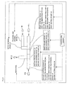
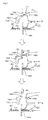
- Fig. 1 shows a flow chart of a manufacturing method of an optical display device.
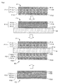
- Fig. 2 shows a schematic view of a sectional structure of first and second laminated optical products F1 and F2, first and second optical members F11 and F22, and a liquid crystal cell W (optical display unit) .
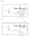
- Fig. 3 shows an example of an arrangement plan view of a manufacturing system of an optical display device in Embodiment 1 of Fig. 1 .
- Figs. 4 to 10C are each a view for explaining an example of the manufacturing system of an optical display device in Embodiment 1.
- Embodiment 1 may have a structure of excluding an optical member judged to contain a defect at a position where the optical member is bonded onto an optical display unit, or may have a structure of excluding the optical member at the upstream side relative to the bonding position. For example, a case where an optical member is excluded for the purpose of sampling for process-inspection, sampling for quality-inspection, or the like is also illustrated, as well as a case where an optical member judged to contain a defect is excluded.
- Examples of the optical member, which is bonded onto the optical display unit include a polarizer film, a retardation film, a viewing angle compensating film and a brightness enhancement film; and any combination of two or more of these films.
- a transparent film for protection may be laminated on one surface or both surfaces of any one of these optical members.
- the second laminated optical product F2 also has the same structure.
- the structure of the first laminated optical product F1 may be different from that of the second laminated optical product F2.
- the first laminated optical product F1 has a laminated structure having a first optical member F11, a releasing film F12, and a surface protecting member F13.
- the first optical member F11 is comprised of a first polarizer F11a, a first polarizer protecting film F11b on one surface thereof through an adhesive layer (not illustrated) interposed therebetween, and a second polarizer protecting film F11c on the other surface thereof through an adhesive layer (not illustrated) interposed therebetween.
- a laminated structure comprised of a polarizer and a polarizer protecting film may be referred as a polarizing plate.
- the first and second polarizer protecting films F11b and F11c may each be, for example, a triacetylcellulose (TAC) film or a polyethylene terephthalate (PET) film.
- TAC triacetylcellulose
- PET polyethylene terephthalate
- the surface protecting film F13 is laid on the first polarizer protecting film F11b through a weak pressure-sensitive adhesive layer F15 interposed therebetween.
- the releasing film F12 is laid on the second polarizer protecting film F11c through a pressure-sensitive adhesive layer F14 interposed therebetween.
- the first and second polarizer protecting films F11b and F11c are not particularly limited, and are each comprised of, for example, a film whose material is a thermoplastic resin excellent in transparency, mechanical strength, thermal stability, water blocking property, isotropy and the like.
- thermoplastic resin examples include cellulose resins such as triacetylcellulose, polyester resin, polyethersulfone resin, polysulfone resin, polycarbonate resin, polyamide resin, polyimide resin, polyolefin resin, (meth) acrylic resin, cyclic polyolefin resin (norbornene based resin), polyarylate resin, polystyrene resin, and polyvinyl alcohol resin; and mixtures thereof.
- cellulose resins such as triacetylcellulose, polyester resin, polyethersulfone resin, polysulfone resin, polycarbonate resin, polyamide resin, polyimide resin, polyolefin resin, (meth) acrylic resin, cyclic polyolefin resin (norbornene based resin), polyarylate resin, polystyrene resin, and polyvinyl alcohol resin; and mixtures thereof.
- the first optical member F11 is an optical film having a multi-layer laminated structure in which various optical layers are laminated onto each other when the layers are practically used.
- the optical layers are not particularly limited.
- An example thereof is a method of applying a hard coating treatment, antireflective treatment or a surface treatment for prevention of sticking, or for diffusion or antiglare to a surface of the polarizer protecting film on which the polarizer is not bonded (a surface on which no adhesive coating layer is laid), or laminating an aligned liquid crystal layer for viewing angle compensation, or the like onto the surface; or a member in which one or more of the following are laminated onto the surface: a reflector, a semi-transmissive plate, a retardation plate (including such as a 1/2 or 1/4 wavelength plate ( ⁇ plate)), or an optical film used to form a liquid crystal display device or the like, such as a viewing angle compensating film.
- the first polarizer F11a is comprised of, for example, a polyvinyl alcohol based film.
- the releasing film F12 is temporarily bonded onto an uncovered surface of the first pressure-sensitive adhesive layer F14 in order to prevent the surface from being polluted, or the like. This makes it possible to prevent the pressure-sensitive adhesive layer F14 from being contacted when the laminated product is in an ordinarily-handled state.
- the releasing film F12 may be an appropriate film according to prior art, for example, an appropriate thin sheet piece which is optionally subjected to coating treatment with an appropriate peeling agent, such as a silicone based, long-chain alkyl based or fluorine-contained peeling agent, or molybdenum sulfite;
- an appropriate peeling agent such as a silicone based, long-chain alkyl based or fluorine-contained peeling agent, or molybdenum sulfite
- examples of the sheet piece include a plastic film, a rubber sheet, a paper piece, a nonwoven cloth, a net, a foamed sheet and a metallic foil piece, and any laminated product thereof.
- the surface protecting member F13 is formed through the weak pressure-sensitive adhesive layer F15.
- a main purpose thereof is the prevention of a scratch or a stain, or the like.
- the surface protecting member may be, for example, an appropriate member according to prior art, for example, an appropriate thin sheet piece which is optionally subjected to coating treatment with an appropriate peeling agent, such as a silicone based, long-chain alkyl based or fluorine-contained peeling agent, or molybdenum sulfite; examples of the sheet piece include a plastic film, a rubber sheet, a paper piece, a nonwoven cloth, a net, a foamed sheet and a metallic foil piece, and any laminated product thereof.
- an appropriate peeling agent such as a silicone based, long-chain alkyl based or fluorine-contained peeling agent, or molybdenum sulfite
- examples of the sheet piece include a plastic film, a rubber sheet, a paper piece, a nonwoven cloth, a net
- the pressure-sensitive adhesive layer F14 and the weak pressure-sensitive adhesive layer F15 are laid in order to attain bonding with other members such as a liquid crystal cell.
- the pressure-sensitive adhesive which constitutes the pressure-sensitive adhesive layer F14 and the weak pressure-sensitive adhesive layer F15, respectively, are not particularly limited, and each of the layers may be formed by an appropriate pressure-sensitive adhesive according to the prior art, such as an acrylic pressure-sensitive adhesive.
- the isolating structure 50 is comprised of walls made of a transparent material, and a framework structure. Blowers 40 are set to the ceiling of the isolating structure 50. The blowers 40 are each equipped with an HEPA filter so that highly clean air is sent into the division wall structure 50 to generate a flow of the clean air. Air discharging openings 50a are made in the wall surface underneath of the division wall structure 50 in order to discharge the air therein to the outside. Filters may also be set to the planes of the openings to prevent invading materials from the outside.
- the division wall structure 50 and the blowers 40 make it possible to maintain a clean environment of the whole of the manufacturing system and appropriately prevent the contamination of foreign substances from the outside. It is unnecessary to render the whole of the factory a clean room since only the manufacturing system is isolated from the outside by the division wall structure 50.
- the defect data obtained in the first defect inspecting device 14 are tied to positional data (for example, position coordinates) thereof, and transmitted to the controlling device so that the data can contribute to a cutting method through a first cutting device 16, which will be described later.
- the defect-containing first laminated optical product F1 is configured to be excluded by a first excluding device 19, which will be described later, so as not to be bonded onto any optical display unit W.
- the first releasing film bonding device 15 adheres the releasing film F12a onto the first optical member F11 through the first pressure-sensitive adhesive layer F14 interposed therebetween.
- the releasing film F12a is unrolled from a material roll 151 of the releasing film F12a, and then the releasing film F12a and the first laminated optical product F1 are sandwiched between one or more roll pairs 152.
- the roller pair(s) 152 allow(s) predetermined pressure to act thereon, thereby bonding the releasing film F12a onto the first optical member F11 through the first pressure-sensitive adhesive layer F14 interposed therebetween.
- a peeling mechanism 171 of the first peeling device has a knife edge region having a sharp tip, and is configured in such a manner that the releasing film F12a is wound around this knife edge region to be transferred reversely, whereby the releasing film F12a is peeled and additionally the first laminated optical product F1 after the releasing film F12a is peeled is sent onto a surface of the optical display unit W.
- the peeled releasing film F12a is wound up around a roll 172.
- a pushing roller 181 is brought into contact with a surface of the surface protecting member F13, and a guide roller 182 is brought into contact with the lower surface of the optical display unit W to press the first laminated optical product F1 onto the optical display unit W surface, thereby bonding the uncovered bonding-surface of the first optical member F11 (the surface of the first pressure-sensitive adhesive layer F14), from which the releasing film F12a has been peeled, onto the optical display unit W surface.
- the pushing roller 181 and the guide roller 182 may each be an elastic roller (made of, for example, a silicone rubber), or a roller made of metal.
- the first optical member F11 is bonded onto one of the surfaces of the optical display unit W.
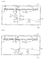
- the following will describe a manufacturing step of bonding a second optical member F21 onto the other surface with reference to Figs. 9 , and 10A to 10C .
- the same steps as in the above-mentioned manufacturing step may be briefly described.
- a peeling mechanism 271 of the second peeling device has a knife edge region having a sharp tip, and is configured in such a manner that the releasing film F22a is wound around this knife edge region to be transferred reversely, whereby the releasing film F22a is peeled and additionally the second laminated optical product F2 after the releasing film F22a is peeled is sent onto a surface of the optical display unit W1.
- the peeled releasing film F22a is wound up around a roll 272.
- a pushing roller 281 is brought into contact with a surface of the surface protecting member F23, and a guide roller 282 is brought into contact with the upper surface of the optical display unit W1 to press the second laminated optical product F2 onto the optical display unit W1 surface, thereby bonding the uncovered bonding-surface of the second optical member F21 (the surface of the second pressure-sensitive adhesive layer F24), from which the releasing film has been peeled, onto the optical display unit W1 surface.
- Step of inspecting an optical display device W12 An inspecting device 30 inspects an optical display device W12 having both surfaces on which the optical members are bonded, respectively.
- the method for the inspection is, for example, a method of applying image-photographing and image-processing to both the surfaces of the optical display device W12 through reflective right.
- Another example thereof is a method of setting a polarizing film for inspection between a CCD camera and an inspection target.
- the algorithm for the image-processing may be a known manner. For example, defects can be detected by, for example, gray-scale decision based on binary image processing.
- the optical display device W12 is a non-defective product or not.
- the display device W12 is carried to the next mounting step.
- the display device W12 is judged to be defective, the display device is subjected to reworking treatment to adhere an optical film thereon newly.
- the resultant product is inspected.
- the product is carried to the mounting step.
- the product is again subjected to reworking treatment or disposal treatment.
- an optical display device By carrying out, in a series of the above-mentioned manufacturing steps, the bonding step for the first optical member F11 and the bonding step for the second optical member F21 in a continuous manufacturing line, an optical display device can be favorably manufactured.
- the above-mentioned individual steps are particularly performed inside an isolating structure isolated from any factory, optical members can be bonded onto an optical display unit in an environment where cleanness is kept, so that a high-quality optical display device can be manufactured.
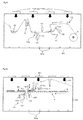
- Figs. 5A to 5C and Figs. 7 to 9 are views for explaining structural examples of the excluding device.
- the structure of the first excluding device 19 is not limited to structures given herein as examples. Various modifications of these structures may be used, and the modifications are included in the technical scope of the present invention.
- the first excluding device 19 for excluding the first laminated optical product F1 is described.
- the action of the first excluding device 19 illustrated in Fig. 5A is described with reference to Fig. 6 .
- Example 1 of the first excluding device 19 has a structure in which the optical member F1 to be excluded is excluded at a position where the optical display unit W and the optical member F11 are bonded onto each other.
- a roller 192 for exclusion may be an elastic roller (made of, for example, silicone rubber), or may be a roller made of metal.
- Example 2 of the first excluding device 19, which is illustrated in Fig. 5B has a structure in which the optical member F11 to be excluded is excluded at the upstream side relative to the position where the optical display unit W and the optical member F11 are bonded onto each other.
- This structure is higher in productivity than the structure of Example 1 since the treatment for bonding the optical display unit W and the optical member F11 onto each other is not interrupted for a long period of time.
- the action of Example 2 of the first excluding device 19, which is illustrated in Fig. 5B is described with reference to Fig. 7 .
- the first excluding device 19 is comprised of a peeling mechanism 195 for peeling the releasing film F12a from the first laminated optical product F1, a tape 191, a roller 192 for exclusion around which the tape 191 is wound, a pushing roller 194 for exclusion which pushes, toward the roller 192 for exclusion, the first optical member F11 to be excluded from which the releasing film F12a is peeled, a winding roller 193 for winding the tape 191 onto which the first optical member F11 to be excluded is bonded, and an accumulating device A arranged at the downstream side of the device.
- the roller 192 for exclusion and the pushing roller 194 for exclusion may each be an elastic roller (made of, for example, silicone rubber), or may be a roller made of metal. The action thereof is as follows.
- Example 3 of the first excluding device 19, which is illustrated in Fig. 5C has a structure in which the optical member F11 to be excluded is excluded at the upstream side relative to the position where the optical display unit W and the optical member F11 are bonded onto each other.
- This structure is higher in productivity than the structure of Example 1 since the treatment for bonding the optical display unit W and the optical member onto each other is not interrupted for a long period of time.
- the action of Example 3 of the first excluding device 19, which is illustrated in Fig. 5C is described with reference to Fig. 8 .
- the first excluding device 19 is comprised of a pressure-sensitive adhesive tape 191, a roller 192 for exclusion around which the pressure-sensitive adhesive tape 191 is wound, and a winding roller 193 for winding the pressure-sensitive adhesive tape 191.
- Example 3 is not equipped with the peeling mechanism 195, the pushing roller 194 nor the accumulating device A as in Example 2. Thus, Example 3 makes it possible to make the device simple. The action thereof is as follows.
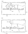
- the following will describe a second excluding device 29 for excluding the second optical member F21 to be excluded.
- the structure and the action of the second excluding device 29 illustrated in Fig. 10A are similar to the structure in Fig. 5A and the action thereof, respectively.
- a guide roller 282 is shifted vertically and upward.
- a roller 292 for exclusion around which a tape 291 is wound is shifted to the bonding position, which is the position where the guide roller 282 is fixed.
- a pushing roller 281 is shifted vertically and upward to push the pressure-sensitive adhesive layer F24 surface of the defect-containing second optical member F21 onto the tape 291 to adhere the second optical member F21 onto the tape 291.
- the defect-containing second optical member F21, together with the tape 291, is then wound around a roller 293.
- the structure of a second excluding device 29 illustrated in Fig. 10B is similar, in effect structure, to the structure in Fig. 5B .
- the structure of a second excluding device 29 illustrated in Fig. 10C is similar to that in Fig. 5C ; the action thereof is also similar although they are different from each other in arrangement position.
- a first laminated optical product F1 in Fig. 11 is carried to face its releasing film F12 upward.
- the structure and the function of each of a first pre-inspection peeling device 13, a first defect inspecting device 14, a first releasing film bonding device 15 and a first cutting device 16 are the similar to those described above. However, the arrangements of these members are different in accordance with the positions of the releasing film F12 and a releasing film F12a.
- a second laminated optical product F2 in Fig. 13 is carried to face its releasing film F22 downward.
- the structure and the function of each of a second pre-inspection peeling device 23, a second defect inspecting device 24, a second releasing film bonding device 25 and a second cutting device 26 are similar to those described above. However, the arrangements of these members are different in accordance with the positions of the releasing film F22 and a releasing film F22a.
- each of a second peeling device 27, a second bonding device 28 and a second excluding device 29 in Figs. 14A to 14C are also similar to those described above.
- the arrangements of these members are different in accordance with the positions of releasing films F22 and F22a.
- the invention provides the following embodiments 1 - 7 as listed hereafter
Landscapes
- Physics & Mathematics (AREA)
- Nonlinear Science (AREA)
- Optics & Photonics (AREA)
- Crystallography & Structural Chemistry (AREA)
- Chemical & Material Sciences (AREA)
- General Physics & Mathematics (AREA)
- Engineering & Computer Science (AREA)
- Mathematical Physics (AREA)
- Manufacturing & Machinery (AREA)
- Mechanical Engineering (AREA)
- Polarising Elements (AREA)
- Liquid Crystal (AREA)
- Devices For Indicating Variable Information By Combining Individual Elements (AREA)
Applications Claiming Priority (3)
| Application Number | Priority Date | Filing Date | Title |
|---|---|---|---|
| JP2008002428 | 2008-01-09 | ||
| JP2008324290A JP4724742B2 (ja) | 2008-01-09 | 2008-12-19 | 光学表示装置の製造システムおよび光学表示装置の製造方法 |
| EP08869545A EP2237249A1 (en) | 2008-01-09 | 2008-12-24 | Manufacturing system of optical display device and manufacturing method of optical display device |
Related Parent Applications (1)
| Application Number | Title | Priority Date | Filing Date |
|---|---|---|---|
| EP08869545.7 Division | 2008-12-24 |
Publications (1)
| Publication Number | Publication Date |
|---|---|
| EP2319689A2 true EP2319689A2 (en) | 2011-05-11 |
Family
ID=41070245
Family Applications (2)
| Application Number | Title | Priority Date | Filing Date |
|---|---|---|---|
| EP08869545A Withdrawn EP2237249A1 (en) | 2008-01-09 | 2008-12-24 | Manufacturing system of optical display device and manufacturing method of optical display device |
| EP11153124A Withdrawn EP2319689A2 (en) | 2008-01-09 | 2008-12-24 | Manufacturing system of optical display device and manufacturing method of optical display device |
Family Applications Before (1)
| Application Number | Title | Priority Date | Filing Date |
|---|---|---|---|
| EP08869545A Withdrawn EP2237249A1 (en) | 2008-01-09 | 2008-12-24 | Manufacturing system of optical display device and manufacturing method of optical display device |
Country Status (7)
| Country | Link |
|---|---|
| US (2) | US20100288432A1 (zh) |
| EP (2) | EP2237249A1 (zh) |
| JP (2) | JP4724742B2 (zh) |
| KR (3) | KR20100103517A (zh) |
| CN (2) | CN101893782B (zh) |
| TW (2) | TW201037651A (zh) |
| WO (1) | WO2009087895A1 (zh) |
Families Citing this family (29)
| Publication number | Priority date | Publication date | Assignee | Title |
|---|---|---|---|---|
| JP4588783B2 (ja) * | 2007-12-11 | 2010-12-01 | 日東電工株式会社 | 光学表示装置の製造方法および光学表示装置の製造システム |
| KR101008418B1 (ko) | 2008-04-08 | 2011-01-14 | 닛토덴코 가부시키가이샤 | 광학 표시 장치의 제조 시스템, 광학 표시 장치의 제조 방법, 배제 장치 및 배제 방법 |
| WO2009128115A1 (ja) | 2008-04-15 | 2009-10-22 | 日東電工株式会社 | 光学フィルム積層体ロールならびにその製造方法および装置 |
| KR101435126B1 (ko) | 2009-12-25 | 2014-09-01 | 닛토덴코 가부시키가이샤 | 액정표시소자의 연속제조방법 및 장치 |
| JP4657378B1 (ja) * | 2010-08-05 | 2011-03-23 | 日東電工株式会社 | ロール原反、並びに、光学表示装置の製造システム及び製造方法 |
| JP5701679B2 (ja) * | 2010-09-03 | 2015-04-15 | 日東電工株式会社 | 矩形形状のパネルに偏光膜を有する光学フィルムを順次的に貼り付ける方法及び装置 |
| JP5474869B2 (ja) | 2010-09-03 | 2014-04-16 | 日東電工株式会社 | 偏光膜を有する積層体ストリップロールの製造方法 |
| JP5181011B2 (ja) * | 2010-10-21 | 2013-04-10 | 日東電工株式会社 | 液晶表示素子の連続製造システムおよび液晶表示素子の連続製造方法 |
| JP5461371B2 (ja) * | 2010-11-25 | 2014-04-02 | 日東電工株式会社 | 液晶表示素子の製造方法および液晶表示素子の製造システム |
| US8633044B2 (en) * | 2011-02-01 | 2014-01-21 | Sharp Kabushiki Kaisha | Display device and method for fabricating same |
| JP4844857B1 (ja) * | 2011-02-23 | 2011-12-28 | 住友化学株式会社 | 回収装置、貼合システム及び回収方法 |
| TWI432838B (zh) * | 2011-02-25 | 2014-04-01 | Innolux Corp | 顯示器及其製造方法 |
| CN103608718B (zh) * | 2011-06-29 | 2017-04-05 | 住友化学株式会社 | 刀刃以及包含该刀刃的液晶显示装置的制造系统 |
| JP5068879B1 (ja) * | 2011-07-19 | 2012-11-07 | 日東電工株式会社 | 液晶表示素子の連続製造方法及び装置 |
| KR101973832B1 (ko) * | 2012-02-29 | 2019-04-29 | 수미토모 케미칼 컴퍼니 리미티드 | 광학 표시 디바이스의 생산 시스템 및 광학 표시 디바이스의 생산 방법 |
| TW201343526A (zh) * | 2012-04-24 | 2013-11-01 | Hon Hai Prec Ind Co Ltd | 供料器 |
| KR101975632B1 (ko) * | 2012-08-08 | 2019-05-07 | 스미또모 가가꾸 가부시키가이샤 | 광학 표시 디바이스의 생산 방법 및 광학 표시 디바이스의 생산 시스템 |
| CN104520916B (zh) * | 2012-08-08 | 2016-10-26 | 住友化学株式会社 | 光学显示器件的生产系统以及生产方法 |
| KR102044588B1 (ko) * | 2012-09-07 | 2019-11-13 | 스미또모 가가꾸 가부시키가이샤 | 광학 부재 접합체의 제조 장치 |
| KR101932562B1 (ko) * | 2012-09-18 | 2018-12-28 | 삼성디스플레이 주식회사 | 필름 부착장치 및 그것을 이용한 필름 부착방법 |
| JP5724147B2 (ja) * | 2013-02-27 | 2015-05-27 | 住友化学株式会社 | 光学表示デバイスの生産システム |
| CN103223765B (zh) * | 2013-03-07 | 2015-12-09 | 京东方科技集团股份有限公司 | 剥膜设备 |
| WO2014185099A1 (ja) * | 2013-05-17 | 2014-11-20 | 住友化学株式会社 | 光学表示デバイスの生産システム |
| KR102182888B1 (ko) * | 2013-10-11 | 2020-11-26 | 삼성디스플레이 주식회사 | 편광 필름 절단용 나이프 및 이를 이용한 편광판 제조 방법 |
| US9498943B2 (en) * | 2014-01-08 | 2016-11-22 | Lg Chem, Ltd. | System for laminating optical film and method for manufacturing display unit using the same |
| KR102184993B1 (ko) * | 2015-04-24 | 2020-12-01 | 엘지전자 주식회사 | 편광 필름 부착 시스템 및 편광 필름 부착 방법 |
| JP2018072689A (ja) * | 2016-11-01 | 2018-05-10 | 日東電工株式会社 | 光学的表示装置を製造する方法 |
| CN107444725B (zh) * | 2017-08-07 | 2019-10-25 | 台州市黄岩康亿丰塑业有限公司 | 一种全自动撕膜装置及其撕膜方法 |
| CN114080149A (zh) * | 2020-08-20 | 2022-02-22 | 三赢科技(深圳)有限公司 | 剥离装置 |
Citations (2)
| Publication number | Priority date | Publication date | Assignee | Title |
|---|---|---|---|---|
| JP2005037416A (ja) | 2003-05-16 | 2005-02-10 | Fuji Photo Film Co Ltd | 偏光板貼合方法及び装置 |
| JP2007140046A (ja) | 2005-11-17 | 2007-06-07 | Nitto Denko Corp | 光学表示装置の製造システム及びその製造方法 |
Family Cites Families (16)
| Publication number | Priority date | Publication date | Assignee | Title |
|---|---|---|---|---|
| JPS5752017A (en) * | 1980-08-08 | 1982-03-27 | Sharp Corp | Tacky-polarizing-plate defective removing device automatic tacky-polarizing-plate sticking machine |
| JP3156419B2 (ja) * | 1993-02-15 | 2001-04-16 | 松下電器産業株式会社 | 異方性導電フィルム保護用セパレータの剥離方法 |
| JPH07270742A (ja) * | 1994-03-30 | 1995-10-20 | Matsushita Electric Ind Co Ltd | テープ圧着装置 |
| KR100513653B1 (ko) * | 1998-08-24 | 2005-11-25 | 비오이 하이디스 테크놀로지 주식회사 | 액정표시소자의 편광판 부착 장치 |
| US6500291B1 (en) * | 1998-09-11 | 2002-12-31 | Hitachi Chemical Co. Ltd. | Device and method for lamination |
| US6383321B2 (en) * | 1999-05-14 | 2002-05-07 | Profold, Inc. | Apparatus and method for applying labels to mail |
| JP4166920B2 (ja) * | 2000-02-24 | 2008-10-15 | リンテック株式会社 | シート剥離装置および方法 |
| US20040095526A1 (en) | 2001-11-27 | 2004-05-20 | Koji Yamabuchi | Liquid crystal panel, method and device for manufacturing liquid crystal panel, and polarizing plate stamping device |
| US7202923B2 (en) | 2001-11-27 | 2007-04-10 | Sharp Kabushiki Kaisha | Liquid crystal display with polarizer with inclined edge portion |
| KR20040002796A (ko) * | 2002-06-28 | 2004-01-07 | 후지 샤신 필름 가부시기가이샤 | 편광판 점착방법 및 그 장치 |
| KR100512192B1 (ko) * | 2003-03-19 | 2005-09-21 | 주식회사 엘지에스 | 광학필름 검사 및 포장장비 |
| JP2005321582A (ja) * | 2004-05-10 | 2005-11-17 | Hitachi Industries Co Ltd | フィルム貼付方法及びフィルム貼付装置 |
| US8040469B2 (en) * | 2004-09-10 | 2011-10-18 | Semiconductor Energy Laboratory Co., Ltd. | Display device, method for manufacturing the same and apparatus for manufacturing the same |
| CN101146682B (zh) * | 2005-03-23 | 2012-02-01 | 富士胶片株式会社 | 用于制造感光性层积体的装置和方法 |
| JP4736717B2 (ja) | 2005-10-28 | 2011-07-27 | ソニー株式会社 | 配線基板の製造方法、及びディスプレイ装置の製造方法 |
| JP2008026631A (ja) | 2006-07-21 | 2008-02-07 | Sharp Corp | 表示パネルの製造方法、表示パネルの検査装置 |
-
2008
- 2008-12-19 JP JP2008324290A patent/JP4724742B2/ja active Active
- 2008-12-24 EP EP08869545A patent/EP2237249A1/en not_active Withdrawn
- 2008-12-24 CN CN2010102289268A patent/CN101893782B/zh active Active
- 2008-12-24 EP EP11153124A patent/EP2319689A2/en not_active Withdrawn
- 2008-12-24 CN CN2008801244152A patent/CN101911156B/zh not_active Expired - Fee Related
- 2008-12-24 US US12/811,640 patent/US20100288432A1/en not_active Abandoned
- 2008-12-24 KR KR1020107013230A patent/KR20100103517A/ko not_active Application Discontinuation
- 2008-12-24 KR KR1020117015297A patent/KR101529757B1/ko active IP Right Grant
- 2008-12-24 WO PCT/JP2008/073420 patent/WO2009087895A1/ja active Application Filing
- 2008-12-24 KR KR1020107016459A patent/KR101099944B1/ko active IP Right Grant
- 2008-12-26 TW TW099120888A patent/TW201037651A/zh unknown
- 2008-12-26 TW TW097151097A patent/TW200951903A/zh unknown
-
2010
- 2010-06-11 JP JP2010134190A patent/JP4759091B2/ja active Active
- 2010-11-22 US US12/951,452 patent/US8500937B2/en not_active Expired - Fee Related
Patent Citations (2)
| Publication number | Priority date | Publication date | Assignee | Title |
|---|---|---|---|---|
| JP2005037416A (ja) | 2003-05-16 | 2005-02-10 | Fuji Photo Film Co Ltd | 偏光板貼合方法及び装置 |
| JP2007140046A (ja) | 2005-11-17 | 2007-06-07 | Nitto Denko Corp | 光学表示装置の製造システム及びその製造方法 |
Also Published As
| Publication number | Publication date |
|---|---|
| KR20100103638A (ko) | 2010-09-27 |
| JP2010191479A (ja) | 2010-09-02 |
| WO2009087895A1 (ja) | 2009-07-16 |
| US8500937B2 (en) | 2013-08-06 |
| CN101911156A (zh) | 2010-12-08 |
| KR20100103517A (ko) | 2010-09-27 |
| KR101099944B1 (ko) | 2011-12-28 |
| EP2237249A1 (en) | 2010-10-06 |
| CN101893782B (zh) | 2013-04-03 |
| JP2009186994A (ja) | 2009-08-20 |
| US20100288432A1 (en) | 2010-11-18 |
| CN101893782A (zh) | 2010-11-24 |
| KR101529757B1 (ko) | 2015-06-17 |
| TWI358687B (zh) | 2012-02-21 |
| JP4759091B2 (ja) | 2011-08-31 |
| US20110061801A1 (en) | 2011-03-17 |
| TW200951903A (en) | 2009-12-16 |
| CN101911156B (zh) | 2012-10-03 |
| TW201037651A (en) | 2010-10-16 |
| KR20110086189A (ko) | 2011-07-27 |
| JP4724742B2 (ja) | 2011-07-13 |
Similar Documents
| Publication | Publication Date | Title |
|---|---|---|
| US8500937B2 (en) | Manufacturing system of optical display device and manufacturing method of optical display device | |
| EP2264516B1 (en) | Method and apparatus for continuously manufacturing liquid crystal display element | |
| US8414993B2 (en) | Roll of continuous web of optical film laminate with predefined slit lines, and method and system for manufacturing the same | |
| EP2415593B1 (en) | Method for manufacturing an optical display device | |
| KR101583101B1 (ko) | 광학 표시 장치의 제조 방법 | |
| EP2246835B1 (en) | Manufacturing system for an optical display device, manufacturing method for an optical display device, removal device, and removal method | |
| JP5792597B2 (ja) | 液晶表示素子の製造方法および液晶表示素子の製造システム | |
| KR20130012150A (ko) | 광학 표시 장치의 제조 방법 및 광학 표시 장치의 제조 시스템 | |
| KR100943404B1 (ko) | 롤 원반 세트 및 롤 원반의 제조 방법 | |
| KR101774623B1 (ko) | 액정 표시 소자의 제조 방법 및 액정 표시 소자의 제조 시스템 |
Legal Events
| Date | Code | Title | Description |
|---|---|---|---|
| PUAI | Public reference made under article 153(3) epc to a published international application that has entered the european phase |
Free format text: ORIGINAL CODE: 0009012 |
|
| AC | Divisional application: reference to earlier application |
Ref document number: 2237249 Country of ref document: EP Kind code of ref document: P |
|
| AK | Designated contracting states |
Kind code of ref document: A2 Designated state(s): AT BE BG CH CY CZ DE DK EE ES FI FR GB GR HR HU IE IS IT LI LT LU LV MC MT NL NO PL PT RO SE SI SK TR |
|
| AX | Request for extension of the european patent |
Extension state: AL BA MK RS |
|
| STAA | Information on the status of an ep patent application or granted ep patent |
Free format text: STATUS: THE APPLICATION HAS BEEN WITHDRAWN |
|
| 18W | Application withdrawn |
Effective date: 20130830 |