EP2309513B1 - Bias sensing in dram sense amplifiers - Google Patents
Bias sensing in dram sense amplifiers Download PDFInfo
- Publication number
- EP2309513B1 EP2309513B1 EP10185622.7A EP10185622A EP2309513B1 EP 2309513 B1 EP2309513 B1 EP 2309513B1 EP 10185622 A EP10185622 A EP 10185622A EP 2309513 B1 EP2309513 B1 EP 2309513B1
- Authority
- EP
- European Patent Office
- Prior art keywords
- voltage
- digit line
- sense amplifier
- coupling
- node
- Prior art date
- Legal status (The legal status is an assumption and is not a legal conclusion. Google has not performed a legal analysis and makes no representation as to the accuracy of the status listed.)
- Expired - Lifetime
Links
- 230000008878 coupling Effects 0.000 claims description 121
- 238000010168 coupling process Methods 0.000 claims description 121
- 238000005859 coupling reaction Methods 0.000 claims description 121
- 239000003990 capacitor Substances 0.000 claims description 64
- 238000002955 isolation Methods 0.000 claims description 55
- 238000000034 method Methods 0.000 claims description 9
- 238000010304 firing Methods 0.000 claims description 7
- 238000010586 diagram Methods 0.000 description 26
- 230000007704 transition Effects 0.000 description 13
- 230000008859 change Effects 0.000 description 10
- 230000007423 decrease Effects 0.000 description 6
- 230000003071 parasitic effect Effects 0.000 description 5
- 230000008901 benefit Effects 0.000 description 3
- 238000004519 manufacturing process Methods 0.000 description 3
- 230000011664 signaling Effects 0.000 description 3
- 230000003247 decreasing effect Effects 0.000 description 2
- 230000003213 activating effect Effects 0.000 description 1
- 238000003491 array Methods 0.000 description 1
- 230000015556 catabolic process Effects 0.000 description 1
- 238000006731 degradation reaction Methods 0.000 description 1
- 238000001514 detection method Methods 0.000 description 1
- 230000003292 diminished effect Effects 0.000 description 1
- 238000007599 discharging Methods 0.000 description 1
- 230000006870 function Effects 0.000 description 1
- 230000008569 process Effects 0.000 description 1
Images


Classifications
-
- G—PHYSICS
- G11—INFORMATION STORAGE
- G11C—STATIC STORES
- G11C11/00—Digital stores characterised by the use of particular electric or magnetic storage elements; Storage elements therefor
- G11C11/21—Digital stores characterised by the use of particular electric or magnetic storage elements; Storage elements therefor using electric elements
- G11C11/34—Digital stores characterised by the use of particular electric or magnetic storage elements; Storage elements therefor using electric elements using semiconductor devices
- G11C11/40—Digital stores characterised by the use of particular electric or magnetic storage elements; Storage elements therefor using electric elements using semiconductor devices using transistors
- G11C11/401—Digital stores characterised by the use of particular electric or magnetic storage elements; Storage elements therefor using electric elements using semiconductor devices using transistors forming cells needing refreshing or charge regeneration, i.e. dynamic cells
- G11C11/4063—Auxiliary circuits, e.g. for addressing, decoding, driving, writing, sensing or timing
- G11C11/407—Auxiliary circuits, e.g. for addressing, decoding, driving, writing, sensing or timing for memory cells of the field-effect type
- G11C11/409—Read-write [R-W] circuits
- G11C11/4091—Sense or sense/refresh amplifiers, or associated sense circuitry, e.g. for coupled bit-line precharging, equalising or isolating
-
- G—PHYSICS
- G11—INFORMATION STORAGE
- G11C—STATIC STORES
- G11C11/00—Digital stores characterised by the use of particular electric or magnetic storage elements; Storage elements therefor
- G11C11/21—Digital stores characterised by the use of particular electric or magnetic storage elements; Storage elements therefor using electric elements
- G11C11/34—Digital stores characterised by the use of particular electric or magnetic storage elements; Storage elements therefor using electric elements using semiconductor devices
- G11C11/40—Digital stores characterised by the use of particular electric or magnetic storage elements; Storage elements therefor using electric elements using semiconductor devices using transistors
- G11C11/401—Digital stores characterised by the use of particular electric or magnetic storage elements; Storage elements therefor using electric elements using semiconductor devices using transistors forming cells needing refreshing or charge regeneration, i.e. dynamic cells
- G11C11/406—Management or control of the refreshing or charge-regeneration cycles
-
- G—PHYSICS
- G11—INFORMATION STORAGE
- G11C—STATIC STORES
- G11C11/00—Digital stores characterised by the use of particular electric or magnetic storage elements; Storage elements therefor
- G11C11/21—Digital stores characterised by the use of particular electric or magnetic storage elements; Storage elements therefor using electric elements
- G11C11/34—Digital stores characterised by the use of particular electric or magnetic storage elements; Storage elements therefor using electric elements using semiconductor devices
- G11C11/40—Digital stores characterised by the use of particular electric or magnetic storage elements; Storage elements therefor using electric elements using semiconductor devices using transistors
- G11C11/401—Digital stores characterised by the use of particular electric or magnetic storage elements; Storage elements therefor using electric elements using semiconductor devices using transistors forming cells needing refreshing or charge regeneration, i.e. dynamic cells
- G11C11/4063—Auxiliary circuits, e.g. for addressing, decoding, driving, writing, sensing or timing
- G11C11/407—Auxiliary circuits, e.g. for addressing, decoding, driving, writing, sensing or timing for memory cells of the field-effect type
- G11C11/4074—Power supply or voltage generation circuits, e.g. bias voltage generators, substrate voltage generators, back-up power, power control circuits
-
- G—PHYSICS
- G11—INFORMATION STORAGE
- G11C—STATIC STORES
- G11C11/00—Digital stores characterised by the use of particular electric or magnetic storage elements; Storage elements therefor
- G11C11/21—Digital stores characterised by the use of particular electric or magnetic storage elements; Storage elements therefor using electric elements
- G11C11/34—Digital stores characterised by the use of particular electric or magnetic storage elements; Storage elements therefor using electric elements using semiconductor devices
- G11C11/40—Digital stores characterised by the use of particular electric or magnetic storage elements; Storage elements therefor using electric elements using semiconductor devices using transistors
- G11C11/401—Digital stores characterised by the use of particular electric or magnetic storage elements; Storage elements therefor using electric elements using semiconductor devices using transistors forming cells needing refreshing or charge regeneration, i.e. dynamic cells
- G11C11/4063—Auxiliary circuits, e.g. for addressing, decoding, driving, writing, sensing or timing
- G11C11/407—Auxiliary circuits, e.g. for addressing, decoding, driving, writing, sensing or timing for memory cells of the field-effect type
- G11C11/409—Read-write [R-W] circuits
- G11C11/4094—Bit-line management or control circuits
-
- G—PHYSICS
- G11—INFORMATION STORAGE
- G11C—STATIC STORES
- G11C7/00—Arrangements for writing information into, or reading information out from, a digital store
- G11C7/06—Sense amplifiers; Associated circuits, e.g. timing or triggering circuits
- G11C7/065—Differential amplifiers of latching type
-
- G—PHYSICS
- G11—INFORMATION STORAGE
- G11C—STATIC STORES
- G11C7/00—Arrangements for writing information into, or reading information out from, a digital store
- G11C7/12—Bit line control circuits, e.g. drivers, boosters, pull-up circuits, pull-down circuits, precharging circuits, equalising circuits, for bit lines
-
- G—PHYSICS
- G11—INFORMATION STORAGE
- G11C—STATIC STORES
- G11C2207/00—Indexing scheme relating to arrangements for writing information into, or reading information out from, a digital store
- G11C2207/005—Transfer gates, i.e. gates coupling the sense amplifier output to data lines, I/O lines or global bit lines
Definitions
- This invention relates to bias sensing in DRAM (dynamic random access memory) sense amplifiers. More particularly, this invention relates to improving the refresh performance of DRAM devices.
- DRAM dynamic random access memory
- sense amplifier devices sense (or sample) and restore electrical charge within each of the memory cells of a given DRAM device.
- a sense amplifier compares the bias voltage on a "reference" digit line with the bias voltage on the digit line connected to the memory cell that is accessed (i.e., read).
- the refresh time or interval between sensing (i.e., reading) and restoring the electrical charge within memory cells is limited to the bias voltage level applied to the reference digit lines. For example, a DRAM memory cell holding an electrical charge representative of a logic "1," is sensed after a finite time interval (refresh time). The sense amplifier then determines that a logic "1" is stored in the memory cell and restores its electrical charge to full value. However, if this refresh duration is too long, the electrical charge stored within this memory cell will degrade too much. When this occurs, the sense amplifier erroneously determines that a logic "0" is stored in the memory cell. Thus, it does not restore the memory cell electrical charge to its full value (i.e., logic "1").
- the refresh time must occur before the voltage on the sensed memory cell digit line drops below the reference digit line bias voltage. Otherwise, the DRAM device erroneously detects a logic "0.” To avoid this, the interval between refresh times must be reduced. However, by reducing the interval between refresh times, the power dissipation within the DRAM device undesirably increases. This becomes progressively problematic as DRAM memory arrays increase in memory capacity as their physical dimensions decrease. By reducing the reference digit line bias voltage, the time interval between the refresh operation (refresh time) increases as a result of providing an increased margin for electrical charge degradation in the memory cell.
- the bias voltage for any particular reference digit line can be reduced to improve the refresh performance.
- this bias voltage threshold level
- the probability of logic "1" detection increases (increasing reliability), and therefore, the required time between refresh operations increases.
- US 5701268 discloses a DRAM with a sensing scheme using capacitive coupling of a signal BS to the digit lines.
- a DRAM device is provided according to independent claim 1 and a method of bias sensing according to independent claim 6.
- An embodiment of a DRAM device in accordance with the invention has first and second digit lines, first and second transistors, sense amplifiers, and first and second voltage coupling/decoupling devices.
- the first and second digit lines have a line connection.
- the first and second transistors each have a first and second terminal. The second terminal of the first transistor couples to the line connection of the first digit line, and the second terminal of the second transistor couples to the line connection of the second digit line.
- This embodiment preferably operates as follows in accordance with the invention: a voltage is applied to the first and second digit lines. Electrical-charge within the memory cell is accessed such that electrical charge sharing occurs between the memory cell and the first digit line, generating a first digit line bias voltage. After the memory cell is accessed, the first isolation transistor is switched ON so that the first sensing connection couples to the first digit line, and the second isolation transistor is switched ON so that the second sensing connection couples to the second digit line. The first and second isolation transistors are then switched OFF so that the first and second sensing connections are electrically isolated from the first and second digit lines. Following the isolation of the sense amplifier connections from the digit lines, a second voltage is capacitively decoupled from the second sense amplifier connection, thus reducing its bias voltage. The DRAM sense amplifier is then fired in order to restore the electrical charge in the memory cell to its designated charge value (logic "1" or logic "0").
- the invention provides DRAM sense amplifier devices with improved bias sensing.
- These sense amplifiers include additional devices for either capacitively decoupling voltages from “reference” digit lines, capacitively coupling voltages onto “active” digit lines, or both.
- a digit line attached to an accessed memory cell is designated as being the “active” digit line.
- a digit line adjacent to the "active" digit line and sharing a common sense amplifier with it is designated as the “reference” digit line. Therefore, “active” and “reference” digit lines dynamically change based on which of the two digit lines is coupled to an accessed memory cell.
- FIG. 1 shows a DRAM sense amplifier circuit 100 within a DRAM array, wherein sense amplifier 100 is connected to a pair of adjacent digit lines 102, 104 through a pair of isolation transistors 106, 108.
- Sense amplifier 100 is coupled to digit line 104 through isolation transistor 108 and coupled to digit line 102 through isolation transistor 106.
- Isolation transistor 108 has terminals 109a, 109b, wherein terminal 109b connects to digit line 104, and terminal 109a couples to sense amplifier 100.
- Isolation transistor 106 has terminals 107a, 107b, wherein terminal 107b connects to second digit line 102, and terminal 107a couples to sense amplifier 100.
- Both isolation transistors 106 and 108 are controlled by a multi-level gate driver 110 that simultaneously applies suitable drive voltages to respective terminals 112, 114 of isolation transistors 106 and 108.
- the drive voltages switch the isolation transistors 106, 108 ON or OFF to control the electrical isolation between digit lines 102, 104 and sense amplifier 100.
- a plurality of memory cells such as memory cells 116 and 150 are connected respectively to digit lines 104 and 102. For clarity, only memory cells 116 and 150 are shown in FIG. 1 .
- Memory cell 116 includes a transistor 118 and a capacitor 120, wherein the gate of transistor 118 connects to a wordline 122 (WL) within the DRAM array.
- Terminal 124 of transistor 118 connects to one end of capacitor 120, wherein the other end of capacitor 120 is grounded.
- the other terminal 126 of transistor 118 connects to digit line 104, at node 128.
- a first voltage coupling/decoupling device 130 is also connected to digit line 104.
- Voltage coupling device 130 includes a coupling/decoupling capacitor 134 and a signal driver device 132.
- Capacitor 134 connects to the output of signal driver 132 at node 136 and connects to digit line 104 at node 138.
- Node 138 is the output of voltage coupling/decoupling device 130.
- a second voltage coupling/decoupling device 140 is connected to digit line 102.
- Voltage coupling device 140 includes capacitor 144 and a second signal driver device 142.
- Capacitor 144 connects to the output of signal driver 142 at node 146 and connects to digit line 102 at node 148.
- Node 148 is the output of voltage coupling/decoupling device 140.
- Sense amplifier device 100 includes an N-sense and a P-sense amplifier.
- the P-sense amplifier includes a cross-coupled PMOS transistor pair having a first PMOS transistor 158 and a second PMOS transistor 160.
- the N-sense amplifier includes a cross coupled NMOS transistor pair having a first NMOS transistor 162 and a second NMOS transistor 164.
- the first PMOS transistor 158 and the first NMOS transistor 162 share a common connection 178 that couples to digit line 102 through node B and isolation transistor 106.
- Second PMOS transistor 160 and second NMOS transistor 164 share a common sensing connection 180 that couples to digit line 104 through node A and isolation transistor 108.
- a common node connection 166 between NMOS transistor pair 162, 164 is normally biased at Vcc/2 (half the supply rail).
- the N-sense amplifier is "fired” or activated by connecting common node connection 166 to ground via turned ON transistor 168. This effectively pulls the common node connection 166 from Vcc/2 to ground (0V).
- a common node connection 170 between PMOS transistor pair 158, 160 is normally biased at about 0V (ground).
- the P-sense amplifier is "fired” or activated by connecting common node connection 170 to Vcc (supply rail) via turned ON transistor 172. This effectively pulls the common node connection from 0V to Vcc.
- both the N-sense and P-sense amplifiers are fired sequentially, with the N-sense amplifier "fired" first, followed by the P-sense amplifier.
- digit line 102 is designated the "reference” digit line 102 and digit line 104 is designated the “active” digit line.
- Voltage coupling/decoupling device 140 decouples a percentage (or fraction) of voltage from the "reference” digit line 102 to reduce the bias voltage on this line.
- Voltage coupling/decoupling device 130 may (optionally) couple a percentage (or fraction) of voltage onto the "active" digit line 104 to increase the bias voltage on this line.
- an increase in the voltage difference between "reference" digit line 102 and “active” digit line 104 can be accomplished by either decoupling voltage from “reference” digit line 102, coupling voltage to "active” digit line 104, or both decoupling voltage from “reference” digit line 102 and coupling voltage onto "active” digit line 104.
- the voltage coupling or decoupling function of voltage coupling/decoupling devices 130, 140 depends on whether their corresponding digit lines are designated as being an "active" digit line or a "reference” digit line.
- FIG. 2 shows an electrical representation of the voltage coupling/decoupling device of FIG. 1 (device 130 or 140).
- the digit line capacitance 204 is denoted by C digitline and is electrically represented as a capacitor having a first connection to digit line 206 and a second connection to ground.
- the digit line capacitance is not a fabricated component such as coupling/decoupling capacitor 210. It is an existing parasitic effect and is therefore not included in the circuit diagram of FIG. 1 .
- Coupling/decoupling capacitor 210 has first and second connection terminals 212, 214, wherein first connection terminal 212 receives a coupling/decoupling drive voltage signal (V CSL ) from a voltage driver device or signal source. Second connection terminal 214 connects to digit line 206 and thus to the first connection of the digit line capacitance 204. A capacitive network is therefore formed between coupling/decoupling capacitor 210 and digit line capacitance 204. By applying a suitable coupling/decoupling drive voltage signal (V CSL ) to connection terminal 212, voltage can be decoupled from, or coupled to, digit line 206.
- V CSL coupling/decoupling drive voltage signal
- ⁇ V NODE C C C + C digitline ⁇ ⁇ V CSL
- ⁇ V NODE the change in voltage on digit line 206
- C C is the capacitance of coupling/decoupling capacitor 210
- C digitline is the capacitance 204 of digit line 206
- ⁇ V CSL is the voltage switching magnitude generated by the coupling/decoupling drive voltage signal (V CSL ).
- FIGS. 5 and 6 illustrate the coupling and decoupling process in more detail.
- coupling/decoupling capacitor 210 is equivalent to coupling/decoupling capacitors 134 and 144.
- V CSL is generated by each signal driver device 132, 142, wherein signal driver device 132 generates a first drive voltage signal (V CSL1 ) and signal driver device 142 generates a second drive voltage signal (V CSL2 ).
- the voltage switching magnitude ⁇ V SCL generated by both drive voltage signals (V CSL ) provides the necessary signaling for coupling or decoupling voltage onto or off of corresponding digit lines 102 and 104.
- the capacitance (C digitline ) 204 of digit line 206 is equivalent to the parasitic capacitance of digit lines 102 and 104.
- the signal driver devices (132 or 142) apply the coupling/decoupling drive voltage signals (V CSL ) onto signal lines 136, 146, where the drive voltage signals (V CSL ) are received by coupling/decoupling capacitors 134, 144, respectively.
- the switching transition direction (low-to-high or high-to-low) of the voltage switching magnitude ⁇ V CSL determines whether voltage is coupled onto or off of the digit line.
- the change in voltage on the digit line ( ⁇ V NODE ) depends on whether a voltage is coupled to the digit line (increasing its bias voltage), or whether a voltage is decoupled from the digit line (reducing its bias voltage).
- Equation (1) that by increasing both the capacitance value of coupling/decoupling capacitor 210 and the voltage switching magnitude ⁇ V CSL , a higher percentage (or fraction) of coupling or decoupling can be achieved.
- the coupling/decoupling capacitance should be approximately one tenth (1/10), or ten percent of the digit line capacitance.
- the coupling/decoupling capacitor must be proportionally increased, which results in the fabrication of larger capacitor devices at the expense of reducing DRAM memory capacity per device size.
- the voltage switching magnitude ( ⁇ V SC ) generated by the signal driver device (132 or 142) is normally between ground and the supply rail (Vcc) in order to maximize the coupling/decoupling fraction.
- the voltage switching magnitude ( ⁇ V SCL ) can be varied (increased or decreased) between a first and second voltage by the signal driver device (132 or 142) in order to vary the coupling/decoupling fraction.
- Both the first and second voltage generated by the signal driver device (132 or 142) are controllably variable.
- more than one coupling/decoupling capacitor may be connected between any given digit line and signal driver device.
- memory cell 116 is considered to hold electrical-charge corresponding to a stored logic "1.”
- digit line 104 is considered the "active" digit line
- adjacent digit line 102 is considered the "reference” digit line.
- both digit lines are pre-biased at Vcc/2 (half the supply rail) prior to firing the N-sense and P-sense amplifiers.
- ⁇ V detectable voltage difference
- gate driver 110 applies a gate voltage to gate terminal 114 and to gate terminal 112 of isolation transistors 108, 106, respectively. This causes both isolation transistors 106, 108 to fully turn ON. With isolation transistor 106 in the ON state, an electrical connection is established between node B and "reference" digit line 102. Sensing connection 178 of sense amplifier 100 connects to node B and therefore to "reference" digit line 102. Similarly, with transistor 108 in the ON state, an electrical connection is established between node A and "active" digit line 104. Sensing connection 180 of sense amplifier 100 connects to node A and therefore to "active" digit line 104.
- the voltage on "active" digit line 104 is received by the sense amplifier's sensing connection 180, and the voltage on "reference” digit line 102 is received by the sense amplifier's sensing connection 178.
- sense amplifier connections 178 and 180 are isolated from respective digit lines 102, 104.
- the voltages on digit lines 102 and 104 remain stored on nodes A and B and sensing connections 178, 180.
- the voltage difference between "active" digit line 104 and "reference" digit line 102 is relatively small. By increasing this voltage difference, both the sensing and the refresh performance of the DRAM device can be improved. In terms of the sensing operation, for example, there will be less probability of sense amplifier 100 erroneously allocating or not allocating the appropriate electrical charge to an accessed memory cell. Also, as the voltage difference between "active" digit line 104 and “reference” digit line 102 increases, the time interval between necessary refresh operations advantageously increases. This is due to the bias voltage on "reference" digit line 102 having a lower voltage threshold, which in turn allows the electrical-charge in accessed memory cell 116 to further deteriorate without becoming undetectable.
- the bias voltage on "active" digit line 104 is still higher than reference digit line 102.
- the bias voltage on "active" digit line 104 must have a lower bias voltage value than that of "reference" digit line 104.
- the aforementioned increase in the voltage difference between "active" digit line 104 and “reference” digit line 102 is achieved by activating voltage coupling/decoupling device 140 such that a fraction or percentage of the existing reference digit line bias voltage (i.e., Vcc/2) is decoupled from reference digit line 102.
- Vcc/2 the existing reference digit line bias voltage
- the sense amplifier's sensing connections 180, 178 receive the respective bias voltages present on the "active" and “reference” digit lines from nodes A and B, respectively.
- isolation transistors 106, 108 Prior to “firing” the P- and N-sense amplifiers, isolation transistors 106, 108 are turned OFF such that the P- and N-sense amplifiers are isolated from the parasitic capacitance of digit lines 102 and 104. Therefore, gate driver 110 removes the previously applied voltage from both isolation transistor gates 112, 114. This turns both transistors 106, 108 OFF, resulting in the electrical isolation of nodes A and B and sensing connections 180, 179 from digit lines 104, 102.
- the increase in the active digit line 104 bias voltage (also present at node A) relative to the reference digit line 102 bias voltage is detected when the N-sense amplifier is "fired.” Once "fired,” transistor 162 turns ON, connecting "reference” digit line 102 to ground (0V). The higher bias voltage on "active" digit line 104 causes transistor 162 to start conducting prior to the conduction of transistor 164. Transistor 164 is thus held in the OFF state when transistor 162 turns ON.
- memory cell 116 stores relatively no electrical-charge (i.e., logic "0")
- the charge sharing will conversely cause the "active" digit line 104 bias voltage to decrease relative to the "reference" digit line 102 bias voltage.
- isolation transistors 106, 108 are turned ON, both the "active" digit line 104 bias voltage and the "reference” digit line 102 bias voltage are received by sensing connections 180, 178, respectively. Isolation transistors 106, 108 are then turned OFF and the sense amplifier is “fired.” The decrease in the "active" digit line 104 bias voltage relative to the "reference" digit line 102 bias voltage is detected by sense amplifier 100.
- a ground reference signal is applied (i.e., 0V) to the "active" digit line 104 via node A and isolation transistor 108 (which is ON).
- 0V ground reference signal
- FIG. 3 illustrates an embodiment of the invention.
- One difference between FIGS. 1 and 3 is that in FIG. 3 coupling/decoupling capacitors 134, 144 are connected to nodes A and B rather than directly to digit lines 104 and 102 as in FIG. 1 .
- sensing connection 180 of sense amplifier 100 connects to terminal 109a of isolation transistor 108 via node A.
- This connection between sense amplifier 100 and isolation transistor 108 is referred to as a first "gut-node" 300.
- Terminal 136 of coupling/decoupling capacitor 134 connects to signal driver 132 (as in FIG. 1 ).
- Terminal 138 of coupling/decoupling capacitor 134 connects to "gut-node" 300 at node A.
- sensing connection 178 of sense amplifier 100 connects to terminal 107b of isolation transistor 106 via node B.
- This connection between sense amplifier 100 and isolation transistor 106 is referred to as a second "gut-node” 302.
- Terminal 146 of coupling/decoupling capacitor 144 connects to signal driver 142 (as in FIG. 1 ).
- Terminal 148 of coupling/decoupling capacitor 144 connects to "gut-node” 302 at node B.
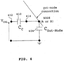
- FIG. 4 shows an electrical representation of the coupling/decoupling device configuration used in FIG. 3 .
- coupling/decoupling capacitors 134 and 144 are respectively connected to "gut-nodes" 300 and 302 as opposed to directly connecting them to the digit lines.
- "Gut-node” capacitance 404 is electrically represented as a capacitor having a first connection to the "gut-node,” and a second connection to ground.
- the "gut-node” capacitance is not a fabricated component, such as coupling/ decoupling capacitor 410. It is an existing parasitic effect and is therefore not included in the circuit diagram of FIG. 3 .
- Coupling/decoupling capacitor 410 has a first and second connection terminal, wherein the first connection terminal 412 receives a coupling/decoupling drive voltage signal (V CSL ) from a voltage driver device or signal source.
- Terminal 414 of coupling/decoupling capacitor 410 connects to the "gut-node” and thus to the first connection of "gut-node” capacitor 404.
- a capacitive network is formed between coupling/decoupling capacitor 410 and "gut-node” capacitor 404, wherein by applying a suitable coupling/decoupling drive voltage signal (V CSL ) to terminal 412 of coupling/decoupling capacitor 410, voltage can be decoupled from, or coupled to, the "gut-node.”
- V CSL coupling/decoupling drive voltage signal
- coupling/decoupling capacitor 410 is equivalent to coupling/decoupling capacitors 134 and 144.
- V CSL is generated by the first or second signal driver devices 132, 142, wherein signal driver device 132 generates a first drive voltage signal (V CSL1 ) and signal driver device 142 generates a second drive voltage signal (V CSL2 ).
- the voltage switching magnitude ⁇ V CSL generated by both drive voltage signals V CSL provides the necessary signaling for coupling or decoupling voltage onto or off of corresponding digit lines 102 and 104.
- the "gut-node” capacitance (C gut-node ) 404 is a parasitic element.
- the signal driver devices (132 or 142) generate the coupling/decoupling drive voltage signals (V CSL ) that are received by coupling/decoupling capacitors 134 and 144.
- the switching transition direction (low-to-high or high-to-low) of the voltage switching magnitude ⁇ V CSL determines whether voltage is coupled to or decoupled from the digit line.
- Equation (2) shows that by increasing the capacitance value of coupling/decoupling capacitor 410 and the voltage level change ⁇ V SCL , a higher percentage (or fraction) of coupling or decoupling can be achieved.
- the advantage of connecting coupling/decoupling capacitors 134 and 144 to "gut-nodes" 300 and 302 is that a higher fraction or percentage of voltage coupling/decoupling can be achieved. This is due to the much lower capacitance value of "gut-nodes" 300 and 302.
- the capacitance of coupling/decoupling capacitors 134 and 144 can be substantially less as a result of the relatively low capacitance of "gut-nodes" 300, 302.
- the relatively high capacitance (C digitline ) of digit lines 102 and 104 required that coupling/decoupling capacitors 134 and 144 also have a proportionally high capacitance as well. Therefore, the "gut-node" capacitance provides voltage coupling with the use of much smaller coupling/decoupling capacitors 134, 144.
- the increase in total capacitance in the denominator will reduce the voltage coupling/decoupling fraction or percentage considerably.
- the advantage of exploiting the "gut-node" capacitance will be substantially diminished if the isolation transistors are fully ON. Both isolation transistors 106, 108 should be either OFF or partially OFF.
- the voltage switching magnitude ( ⁇ V CSL ) generated by the signal driver device (132 or 142) is normally between ground and the supply rail (Vcc) in order to maximize the coupling/decoupling fraction.
- the voltage level change value ( ⁇ V CSL ) can be varied (increased or decreased) between a first and a second voltage by the signal driver device (132 or 142) in order to vary the coupling/decoupling fraction.
- more than one coupling/decoupling capacitor may be connected between any given digit line and signal driver device.
- timing diagram 500 in order to access memory cell 116, at a time t 0 , a wordline voltage signal 502 (Vccp) is applied to gate 122 of transistor 118.
- Vccp wordline voltage signal 502
- the magnitude of this voltage signal ensures that memory cell 116 is fully turned ON during the subsequent sense and restore operations.
- an ISO gate signal 506 is raised from Vcc/2 to Vccp so that the gate voltages of isolation transistors 106 and 108 are raised above their threshold value.
- This turns isolation transistors 106, 108 ON such that the voltage on "active" digit line 104 and “reference” digit line 102 are received by respective "gut-nodes" 300 and 302, and are therefore received by sensing connections 180 and 178 of sensing amplifier 100.
- Timing diagram 508 shows the bias voltages at gut-nodes 300 and 302. As illustrated, prior to time t 0 , both gut-nodes 300, 302 are biased at Vcc/2. At t 0 , once memory cell 116 (i.e., stored logic "1") and isolation transistor 108 are accessed, electrical-charge sharing occurs between "active" digit line 104 and memory cell 116. This causes a voltage increase (V2) in the "active" digit line bias voltage. As the "active" digit line 104 and gut-node 300 are connected via the turned ON isolation transistor, the first "gut-node” bias voltage 510 is charged to the increased “active" digit line bias voltage (V2 increase). Also following time t 0 , the second "gut-node” bias voltage 512 is the same as the “reference" digit line bias voltage.
- the gate signal 506 applied to isolation transistors 106 and 108 returns to Vcc/2 (or lower). This causes transistors 106, 108 to partially or completely turn OFF (depending on device threshold).
- digit lines 102 and 104 are isolated from respective gut-nodes 302 and 300.
- both the increased "active" digit line bias voltage and the "reference” digit line bias voltage are present (stored) on both "gut-node” 300 and "gut-node 302 respectively. Therefore, these bias voltages are also received at sensing connections 178 and 180 of sensing amplifier 100.
- Timing diagram 514 shows the coupling/decoupling drive voltage signal (V CSL2 ) 516 generated by signal driver device 142.
- V CSL2 the coupling/decoupling drive voltage signal 516 makes a high-to-low voltage transition from Vcc to ground ( ⁇ V CSL) .
- the N-sense amplifier is "fired," wherein the common node bias voltage 522 on common node connection 166 is dropped from Vcc/2 (half the supply voltage) to near ground. This connects gut-node 302 to ground, as illustrated in timing diagram 508 at time t 4 .
- the P-sense amplifier is "fired,” wherein the common node bias voltage 524 on common node connection 170 is raised from ground (0V) to Vcc (supply voltage). This connects gut-node 300 to the supply voltage, as illustrated in timing diagram 508 at time instant t 6 .
- the isolation transistors are turned ON by increasing the voltage of the ISO gate signal 506 from Vcc/2 to Vccp. Consequently, an electrical path between "gut-node” 300 and "active" digit line 104 is established. Therefore, the applied supply voltage on "gut-node” 300 is also received by "active" digit line 104. Because memory cell transistor 118 is still fully ON, memory cell capacitor 120 is fully charged by the supply voltage. Thus, the electrical charge within memory cell 116 is fully restored by the application of a charge voltage (e.g., supply voltage) to "active" digit line 104.
- a charge voltage e.g., supply voltage
- FIG. 6 illustrates different signaling schemes for coupling and decoupling voltage onto or off of digit lines and their respective "gut-nodes" during the sensing operation of the sense amplifiers.
- Timing diagram 602 is identical to timing diagram 514 shown in FIG. 5 .
- Timing diagram 602 shows that at time t 2 , the second coupling/decoupling drive voltage signal 604 (V CSL2 ) makes a high-to-low voltage transition ( ⁇ V CSL ) from Vcc to ground. This provides voltage decoupling from the "reference" digit line bias voltage stored on "gut-node” 302.
- the first coupling/decoupling drive voltage signal 606 (V CSL1 ) is in the "logic high” state and makes no voltage transition at time t 2 . Therefore, no voltage change is applied to the "active" digit line bias voltage stored on "gut-node” 300.
- Timing diagram 608 shows the first coupling/decoupling drive voltage signal 610 (V CSL1 ) in the "logic low” state. Once again, no voltage change is applied to the "active" digit line bias voltage stored on "gut-node” 300. Thus, the "gut-node” bias voltage remains unchanged (i.e., no coupling or decoupling). If the voltage is kept constant, no voltage coupling or decoupling will occur.
- the refresh performance of a DRAM device can also be improved by both coupling bias voltage onto an active digit line or "gut-node,” and decoupling bias voltage from a "reference” digit line or “gut-node.”
- the coupling/decoupling drive signals for achieving this are shown in timing diagram 612.
- Timing diagram 612 shows that at time t 2 , second coupling/decoupling drive voltage signal 614 (V CSL2 ) makes a high-to-low voltage transition ( ⁇ V CSL ) from Vcc to ground. This provides voltage decoupling from the "reference" digit line bias voltage stored on "gut-node” 302.
- first coupling/decoupling drive voltage signal 616 makes a low-to-high voltage transition ( ⁇ V CSL ) from ground to Vcc. This provides voltage coupling onto the "active" digit line bias voltage stored on "gut-node” 300. This couples a percentage or fraction of the low-to-high voltage transition ( ⁇ V CSL ) onto the "active" digit line or "gut-node,” wherein the fraction or percentage of coupling is determined by the capacitor values in the formed capacitor network.
- the first coupling/decoupling drive voltage signal 616 (V CSL1 ) makes a low-to-high voltage transition ( ⁇ V CSL ) and couples a percentage or fraction of the low-to-high voltage transition ( ⁇ V CSL ) onto the "active" digit line or "gut-node.”
- the second coupling/decoupling drive voltage signal 614 (V SCL2 ) may be kept at a constant voltage (i.e., no voltage transition) such that voltage is not decoupled from the "reference" digit line.
- the coupling/decoupling fraction or coupling/decoupling percentage is determined by the capacitance of the coupling/decoupling capacitor (e.g., capacitor 134) and the digit line capacitance (e.g., C digitline of "active" digit line 104).
- the coupling fraction or coupling percentage is determined by the capacitance of the coupling/decoupling capacitor (e.g., capacitor 134) and the corresponding "gut-node” capacitance (e.g., C gut-node located at 300).
- coupling/decoupling devices are connected to any pair of digit lines that correspond to a particular sense amplifier.
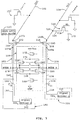
- FIG. 7 shows a system that incorporates the invention.
- System 700 includes a plurality of DRAM chips 775, a processor 770, a memory controller 772, input devices 774, output devices 776, and optional storage devices 778.
- DRAM chips 775 include the embodiment illustrated in FIG. 3 .
- Data and control signals are transferred between processor 770 and memory controller 772 via bus 771.
- data and control signals are transferred between memory controller 772 and DRAM chips 775 via bus 773.
- Input devices 774 can include, for example, a keyboard, a mouse, a touch-pad display screen, or any other appropriate device that allows a user to enter information into system 700.
- DRAM sense amplifiers are provided that have improved refresh performances.
- One skilled in the art will appreciate that the invention can be practiced by other than the described embodiment, which is presented for purposes of illustration and not of limitation, and the invention is limited only by the claims which follow.
Landscapes
- Engineering & Computer Science (AREA)
- Microelectronics & Electronic Packaging (AREA)
- Computer Hardware Design (AREA)
- Dram (AREA)
- Semiconductor Memories (AREA)
Applications Claiming Priority (3)
| Application Number | Priority Date | Filing Date | Title |
|---|---|---|---|
| US10/233,871 US6757202B2 (en) | 2002-08-29 | 2002-08-29 | Bias sensing in DRAM sense amplifiers |
| PCT/US2003/026736 WO2004021354A1 (en) | 2002-08-29 | 2003-08-26 | Bias sensing in dram sense amplifiers |
| EP03791803.4A EP1540655B1 (en) | 2002-08-29 | 2003-08-26 | Bias sensing in dram sense amplifiers |
Related Parent Applications (3)
| Application Number | Title | Priority Date | Filing Date |
|---|---|---|---|
| EP03791803.4 Division | 2003-08-26 | ||
| EP03791803.4A Division-Into EP1540655B1 (en) | 2002-08-29 | 2003-08-26 | Bias sensing in dram sense amplifiers |
| EP03791803.4A Division EP1540655B1 (en) | 2002-08-29 | 2003-08-26 | Bias sensing in dram sense amplifiers |
Publications (3)
| Publication Number | Publication Date |
|---|---|
| EP2309513A2 EP2309513A2 (en) | 2011-04-13 |
| EP2309513A3 EP2309513A3 (en) | 2011-05-25 |
| EP2309513B1 true EP2309513B1 (en) | 2019-07-10 |
Family
ID=31977313
Family Applications (2)
| Application Number | Title | Priority Date | Filing Date |
|---|---|---|---|
| EP10185622.7A Expired - Lifetime EP2309513B1 (en) | 2002-08-29 | 2003-08-26 | Bias sensing in dram sense amplifiers |
| EP03791803.4A Expired - Lifetime EP1540655B1 (en) | 2002-08-29 | 2003-08-26 | Bias sensing in dram sense amplifiers |
Family Applications After (1)
| Application Number | Title | Priority Date | Filing Date |
|---|---|---|---|
| EP03791803.4A Expired - Lifetime EP1540655B1 (en) | 2002-08-29 | 2003-08-26 | Bias sensing in dram sense amplifiers |
Country Status (9)
| Country | Link |
|---|---|
| US (6) | US6757202B2 (enExample) |
| EP (2) | EP2309513B1 (enExample) |
| JP (2) | JP2005536827A (enExample) |
| KR (2) | KR100939054B1 (enExample) |
| CN (1) | CN1685438B (enExample) |
| AU (1) | AU2003260089A1 (enExample) |
| SG (1) | SG153662A1 (enExample) |
| TW (1) | TWI311319B (enExample) |
| WO (1) | WO2004021354A1 (enExample) |
Families Citing this family (22)
| Publication number | Priority date | Publication date | Assignee | Title |
|---|---|---|---|---|
| US6978088B2 (en) * | 2002-08-27 | 2005-12-20 | Pentax Corporation | Optical element retracting mechanism for a retractable lens |
| US6757202B2 (en) * | 2002-08-29 | 2004-06-29 | Micron Technology, Inc. | Bias sensing in DRAM sense amplifiers |
| US20040257882A1 (en) * | 2003-06-20 | 2004-12-23 | Blaine Stackhouse | Bias generation having adjustable range and resolution through metal programming |
| US8324872B2 (en) * | 2004-03-26 | 2012-12-04 | Marvell World Trade, Ltd. | Voltage regulator with coupled inductors having high coefficient of coupling |
| US7372092B2 (en) * | 2005-05-05 | 2008-05-13 | Micron Technology, Inc. | Memory cell, device, and system |
| KR100869541B1 (ko) * | 2006-05-26 | 2008-11-19 | 삼성전자주식회사 | 오픈 비트라인 구조의 메모리 장치 및 이 장치의 비트라인데이터 센싱 방법 |
| US7408813B2 (en) * | 2006-08-03 | 2008-08-05 | Micron Technology, Inc. | Block erase for volatile memory |
| TWI381394B (zh) * | 2008-06-09 | 2013-01-01 | Promos Technologies Inc | 動態隨機存取記憶體之資料感測方法 |
| US8625372B2 (en) | 2008-12-24 | 2014-01-07 | Stmicroelectronics International N.V. | Noise tolerant sense circuit |
| US8164942B2 (en) * | 2010-02-01 | 2012-04-24 | International Business Machines Corporation | High performance eDRAM sense amplifier |
| US9087559B2 (en) * | 2012-12-27 | 2015-07-21 | Intel Corporation | Memory sense amplifier voltage modulation |
| US9053960B2 (en) * | 2013-03-04 | 2015-06-09 | Qualcomm Incorporated | Decoupling capacitor for integrated circuit |
| WO2014151659A1 (en) * | 2013-03-15 | 2014-09-25 | Silicon Image, Inc. | Method and apparatus for implementing wide data range and wide common-mode receivers |
| US9245604B2 (en) | 2013-05-08 | 2016-01-26 | International Business Machines Corporation | Prioritizing refreshes in a memory device |
| US9224450B2 (en) * | 2013-05-08 | 2015-12-29 | International Business Machines Corporation | Reference voltage modification in a memory device |
| US9318187B2 (en) * | 2013-07-23 | 2016-04-19 | Micron Technology, Inc. | Method and apparatus for sensing in a memory |
| US9378781B1 (en) | 2015-04-09 | 2016-06-28 | Qualcomm Incorporated | System, apparatus, and method for sense amplifiers |
| US9378780B1 (en) | 2015-06-16 | 2016-06-28 | National Tsing Hua University | Sense amplifier |
| US10395697B1 (en) * | 2018-02-08 | 2019-08-27 | Micron Technology, Inc. | Self-referencing sensing schemes with coupling capacitance |
| DE102018202871B4 (de) * | 2018-02-26 | 2019-09-12 | Dialog Semiconductor (Uk) Limited | Leistungseffiziente Treiberschaltung, die Ladungsrückgewinnung nutzt, und Verfahren zum Ansteuern einer Last |
| US10699755B2 (en) * | 2018-09-18 | 2020-06-30 | Micron Technology, Inc. | Apparatuses and methods for plate coupled sense amplifiers |
| US11727980B2 (en) * | 2021-03-30 | 2023-08-15 | Micron Technology, Inc. | Apparatuses and methods for single-ended global and local input/output architecture |
Family Cites Families (30)
| Publication number | Priority date | Publication date | Assignee | Title |
|---|---|---|---|---|
| US4625300A (en) * | 1982-12-01 | 1986-11-25 | Texas Instruments Incorporated | Single-ended sense amplifier for dynamic memory array |
| JPS60236191A (ja) | 1984-05-08 | 1985-11-22 | Matsushita Electric Ind Co Ltd | 半導体記憶装置 |
| JPS61217986A (ja) * | 1985-03-25 | 1986-09-27 | Hitachi Ltd | ダイナミツク型ram |
| JPS63282993A (ja) * | 1987-05-15 | 1988-11-18 | Mitsubishi Electric Corp | 半導体ダイナミック・ランダム・アクセス・メモリ |
| JPS63282994A (ja) * | 1987-05-15 | 1988-11-18 | Mitsubishi Electric Corp | 半導体ダイナミック・ランダム・アクセス・メモリ |
| JPH0758592B2 (ja) * | 1987-11-30 | 1995-06-21 | 日本電気株式会社 | 半導体メモリ |
| JPH03296989A (ja) * | 1990-04-16 | 1991-12-27 | Nec Corp | ダイナミック型センスアンプ |
| US5157634A (en) | 1990-10-23 | 1992-10-20 | International Business Machines Corporation | Dram having extended refresh time |
| JP2817552B2 (ja) * | 1992-01-30 | 1998-10-30 | 日本電気株式会社 | 半導体メモリ装置 |
| JPH05210975A (ja) * | 1992-01-30 | 1993-08-20 | Nec Corp | ダイナミックram |
| US5291437A (en) | 1992-06-25 | 1994-03-01 | Texas Instruments Incorporated | Shared dummy cell |
| JP3315293B2 (ja) * | 1995-01-05 | 2002-08-19 | 株式会社東芝 | 半導体記憶装置 |
| JP3272193B2 (ja) * | 1995-06-12 | 2002-04-08 | 株式会社東芝 | 半導体装置およびその動作方法 |
| KR0177776B1 (ko) * | 1995-08-23 | 1999-04-15 | 김광호 | 고집적 반도체 메모리 장치의 데이타 센싱회로 |
| KR100214462B1 (ko) | 1995-11-27 | 1999-08-02 | 구본준 | 반도체메모리셀의 라이트 방법 |
| JP3824370B2 (ja) * | 1997-03-03 | 2006-09-20 | 富士通株式会社 | 半導体装置 |
| JP3296989B2 (ja) | 1997-03-31 | 2002-07-02 | ユニ・チャーム株式会社 | 水解性シート及びその製造方法 |
| JPH10302469A (ja) * | 1997-04-25 | 1998-11-13 | Fujitsu Ltd | 半導体記憶装置 |
| JPH1144292A (ja) | 1997-07-25 | 1999-02-16 | Ishikawajima Harima Heavy Ind Co Ltd | 訓練シミュレータのポンプモデル |
| DE19735137C1 (de) | 1997-08-13 | 1998-10-01 | Siemens Ag | Schaltungsvorrichtung für die Bewertung des Dateninhalts von Speicherzellen |
| US5995421A (en) * | 1998-05-29 | 1999-11-30 | Stmicroelectronics, Inc. | Circuit and method for reading a memory cell |
| JP2000057772A (ja) | 1998-08-12 | 2000-02-25 | Nec Corp | 半導体記憶装置 |
| JP2000187985A (ja) | 1998-12-24 | 2000-07-04 | Hitachi Ltd | 半導体記憶装置 |
| US6157578A (en) * | 1999-07-15 | 2000-12-05 | Stmicroelectronics, Inc. | Method and apparatus for accessing a memory device |
| JP2001351383A (ja) * | 2000-06-07 | 2001-12-21 | Mitsubishi Electric Corp | 半導体集積回路装置 |
| FR2810782B1 (fr) * | 2000-06-26 | 2002-10-04 | St Microelectronics Sa | Procede de commande d'un acces en lesture d'une memoire vive dynamique et memoire correspondante |
| JP3856424B2 (ja) * | 2000-12-25 | 2006-12-13 | 株式会社東芝 | 半導体記憶装置 |
| KR100393224B1 (ko) * | 2001-06-30 | 2003-07-31 | 삼성전자주식회사 | 비트라인 쌍들의 부하를 차단하는 회로를 구비하는 반도체메모리장치 |
| US6757202B2 (en) * | 2002-08-29 | 2004-06-29 | Micron Technology, Inc. | Bias sensing in DRAM sense amplifiers |
| US6862208B2 (en) * | 2003-04-11 | 2005-03-01 | Freescale Semiconductor, Inc. | Memory device with sense amplifier and self-timed latch |
-
2002
- 2002-08-29 US US10/233,871 patent/US6757202B2/en not_active Expired - Lifetime
-
2003
- 2003-08-26 EP EP10185622.7A patent/EP2309513B1/en not_active Expired - Lifetime
- 2003-08-26 JP JP2004531500A patent/JP2005536827A/ja active Pending
- 2003-08-26 KR KR1020087020886A patent/KR100939054B1/ko not_active Expired - Lifetime
- 2003-08-26 AU AU2003260089A patent/AU2003260089A1/en not_active Abandoned
- 2003-08-26 CN CN038226332A patent/CN1685438B/zh not_active Expired - Lifetime
- 2003-08-26 SG SG200701489-7A patent/SG153662A1/en unknown
- 2003-08-26 WO PCT/US2003/026736 patent/WO2004021354A1/en not_active Ceased
- 2003-08-26 KR KR1020057003148A patent/KR100976830B1/ko not_active Expired - Lifetime
- 2003-08-26 EP EP03791803.4A patent/EP1540655B1/en not_active Expired - Lifetime
- 2003-08-29 TW TW092123964A patent/TWI311319B/zh not_active IP Right Cessation
-
2004
- 2004-06-23 US US10/874,995 patent/US7072235B2/en not_active Expired - Lifetime
-
2006
- 2006-06-13 US US11/452,783 patent/US7567477B2/en not_active Expired - Lifetime
-
2009
- 2009-07-07 US US12/498,541 patent/US7903488B2/en not_active Expired - Lifetime
- 2009-08-11 JP JP2009186921A patent/JP2009301700A/ja active Pending
-
2011
- 2011-03-02 US US13/039,169 patent/US8767496B2/en not_active Expired - Lifetime
-
2014
- 2014-06-26 US US14/316,368 patent/US9633714B2/en not_active Expired - Fee Related
Non-Patent Citations (1)
| Title |
|---|
| None * |
Also Published As
| Publication number | Publication date |
|---|---|
| EP1540655B1 (en) | 2019-07-03 |
| KR100976830B1 (ko) | 2010-08-20 |
| US20040042276A1 (en) | 2004-03-04 |
| JP2005536827A (ja) | 2005-12-02 |
| US20090323448A1 (en) | 2009-12-31 |
| US20040228195A1 (en) | 2004-11-18 |
| KR20080083215A (ko) | 2008-09-16 |
| US6757202B2 (en) | 2004-06-29 |
| EP2309513A2 (en) | 2011-04-13 |
| US7903488B2 (en) | 2011-03-08 |
| AU2003260089A1 (en) | 2004-03-19 |
| TWI311319B (en) | 2009-06-21 |
| US9633714B2 (en) | 2017-04-25 |
| EP1540655A1 (en) | 2005-06-15 |
| TW200426836A (en) | 2004-12-01 |
| US20110157962A1 (en) | 2011-06-30 |
| US20140307516A1 (en) | 2014-10-16 |
| EP2309513A3 (en) | 2011-05-25 |
| US8767496B2 (en) | 2014-07-01 |
| KR100939054B1 (ko) | 2010-01-28 |
| KR20070089894A (ko) | 2007-09-04 |
| US20060280011A1 (en) | 2006-12-14 |
| US7072235B2 (en) | 2006-07-04 |
| JP2009301700A (ja) | 2009-12-24 |
| WO2004021354A1 (en) | 2004-03-11 |
| SG153662A1 (en) | 2009-07-29 |
| CN1685438A (zh) | 2005-10-19 |
| CN1685438B (zh) | 2011-11-16 |
| US7567477B2 (en) | 2009-07-28 |
Similar Documents
| Publication | Publication Date | Title |
|---|---|---|
| US9633714B2 (en) | Methods for bias sensing in DRAM sense amplifiers through voltage-coupling/decoupling devices | |
| US5701268A (en) | Sense amplifier for integrated circuit memory devices having boosted sense and current drive capability and methods of operating same | |
| US5917746A (en) | Cell plate structure for a ferroelectric memory | |
| US5905672A (en) | Ferroelectric memory using ferroelectric reference cells | |
| US5574681A (en) | Method for DRAM sensing current control | |
| EP0061289B1 (en) | Dynamic type semiconductor monolithic memory | |
| US5650970A (en) | semiconductor memory device having a flash write function | |
| US6049493A (en) | Semiconductor memory device having a precharge device | |
| US7663952B2 (en) | Capacitor supported precharging of memory digit lines | |
| US7251153B2 (en) | Memory | |
| WO1994003900A1 (en) | Six transistor dynamic content addressable memory circuit | |
| US6111803A (en) | Reduced cell voltage for memory device | |
| US4734890A (en) | Dynamic RAM having full-sized dummy cell | |
| US20010010641A1 (en) | Memory array architecture, method of operating a dynamic random access memory, and method of manufacturing a dynamic random access memory | |
| KR100373352B1 (ko) | 셀 저장노드의 전압다운 보상을 위한 저항을 갖는 강유전체 메모리 장치의 메모리 셀 | |
| JPS63244395A (ja) | ダイナミツク型半導体記憶装置 | |
| JPS63244489A (ja) | ダイナミツクramのセンスアンプ回路の駆動方法 |
Legal Events
| Date | Code | Title | Description |
|---|---|---|---|
| PUAI | Public reference made under article 153(3) epc to a published international application that has entered the european phase |
Free format text: ORIGINAL CODE: 0009012 |
|
| AC | Divisional application: reference to earlier application |
Ref document number: 1540655 Country of ref document: EP Kind code of ref document: P |
|
| AK | Designated contracting states |
Kind code of ref document: A2 Designated state(s): AT BE BG CH CY CZ DE DK EE ES FI FR GB GR HU IE IT LI LU MC NL PT RO SE SI SK TR |
|
| AX | Request for extension of the european patent |
Extension state: AL LT LV MK |
|
| PUAL | Search report despatched |
Free format text: ORIGINAL CODE: 0009013 |
|
| RIN1 | Information on inventor provided before grant (corrected) |
Inventor name: MCELROY, DAVID J. Inventor name: CASPER, STEPHEN L. |
|
| AK | Designated contracting states |
Kind code of ref document: A3 Designated state(s): AT BE BG CH CY CZ DE DK EE ES FI FR GB GR HU IE IT LI LU MC NL PT RO SE SI SK TR |
|
| AX | Request for extension of the european patent |
Extension state: AL LT LV MK |
|
| 17P | Request for examination filed |
Effective date: 20111125 |
|
| 17Q | First examination report despatched |
Effective date: 20130911 |
|
| STAA | Information on the status of an ep patent application or granted ep patent |
Free format text: STATUS: EXAMINATION IS IN PROGRESS |
|
| GRAP | Despatch of communication of intention to grant a patent |
Free format text: ORIGINAL CODE: EPIDOSNIGR1 |
|
| STAA | Information on the status of an ep patent application or granted ep patent |
Free format text: STATUS: GRANT OF PATENT IS INTENDED |
|
| INTG | Intention to grant announced |
Effective date: 20190207 |
|
| GRAS | Grant fee paid |
Free format text: ORIGINAL CODE: EPIDOSNIGR3 |
|
| GRAA | (expected) grant |
Free format text: ORIGINAL CODE: 0009210 |
|
| STAA | Information on the status of an ep patent application or granted ep patent |
Free format text: STATUS: THE PATENT HAS BEEN GRANTED |
|
| AC | Divisional application: reference to earlier application |
Ref document number: 1540655 Country of ref document: EP Kind code of ref document: P |
|
| AK | Designated contracting states |
Kind code of ref document: B1 Designated state(s): AT BE BG CH CY CZ DE DK EE ES FI FR GB GR HU IE IT LI LU MC NL PT RO SE SI SK TR |
|
| REG | Reference to a national code |
Ref country code: GB Ref legal event code: FG4D |
|
| REG | Reference to a national code |
Ref country code: CH Ref legal event code: EP Ref country code: AT Ref legal event code: REF Ref document number: 1154400 Country of ref document: AT Kind code of ref document: T Effective date: 20190715 |
|
| REG | Reference to a national code |
Ref country code: DE Ref legal event code: R096 Ref document number: 60352135 Country of ref document: DE |
|
| REG | Reference to a national code |
Ref country code: IE Ref legal event code: FG4D |
|
| REG | Reference to a national code |
Ref country code: NL Ref legal event code: MP Effective date: 20190710 |
|
| REG | Reference to a national code |
Ref country code: AT Ref legal event code: MK05 Ref document number: 1154400 Country of ref document: AT Kind code of ref document: T Effective date: 20190710 |
|
| PG25 | Lapsed in a contracting state [announced via postgrant information from national office to epo] |
Ref country code: FI Free format text: LAPSE BECAUSE OF FAILURE TO SUBMIT A TRANSLATION OF THE DESCRIPTION OR TO PAY THE FEE WITHIN THE PRESCRIBED TIME-LIMIT Effective date: 20190710 Ref country code: BG Free format text: LAPSE BECAUSE OF FAILURE TO SUBMIT A TRANSLATION OF THE DESCRIPTION OR TO PAY THE FEE WITHIN THE PRESCRIBED TIME-LIMIT Effective date: 20191010 Ref country code: SE Free format text: LAPSE BECAUSE OF FAILURE TO SUBMIT A TRANSLATION OF THE DESCRIPTION OR TO PAY THE FEE WITHIN THE PRESCRIBED TIME-LIMIT Effective date: 20190710 Ref country code: PT Free format text: LAPSE BECAUSE OF FAILURE TO SUBMIT A TRANSLATION OF THE DESCRIPTION OR TO PAY THE FEE WITHIN THE PRESCRIBED TIME-LIMIT Effective date: 20191111 Ref country code: NL Free format text: LAPSE BECAUSE OF FAILURE TO SUBMIT A TRANSLATION OF THE DESCRIPTION OR TO PAY THE FEE WITHIN THE PRESCRIBED TIME-LIMIT Effective date: 20190710 Ref country code: AT Free format text: LAPSE BECAUSE OF FAILURE TO SUBMIT A TRANSLATION OF THE DESCRIPTION OR TO PAY THE FEE WITHIN THE PRESCRIBED TIME-LIMIT Effective date: 20190710 |
|
| PG25 | Lapsed in a contracting state [announced via postgrant information from national office to epo] |
Ref country code: ES Free format text: LAPSE BECAUSE OF FAILURE TO SUBMIT A TRANSLATION OF THE DESCRIPTION OR TO PAY THE FEE WITHIN THE PRESCRIBED TIME-LIMIT Effective date: 20190710 Ref country code: GR Free format text: LAPSE BECAUSE OF FAILURE TO SUBMIT A TRANSLATION OF THE DESCRIPTION OR TO PAY THE FEE WITHIN THE PRESCRIBED TIME-LIMIT Effective date: 20191011 |
|
| PG25 | Lapsed in a contracting state [announced via postgrant information from national office to epo] |
Ref country code: TR Free format text: LAPSE BECAUSE OF FAILURE TO SUBMIT A TRANSLATION OF THE DESCRIPTION OR TO PAY THE FEE WITHIN THE PRESCRIBED TIME-LIMIT Effective date: 20190710 |
|
| PG25 | Lapsed in a contracting state [announced via postgrant information from national office to epo] |
Ref country code: EE Free format text: LAPSE BECAUSE OF FAILURE TO SUBMIT A TRANSLATION OF THE DESCRIPTION OR TO PAY THE FEE WITHIN THE PRESCRIBED TIME-LIMIT Effective date: 20190710 Ref country code: IT Free format text: LAPSE BECAUSE OF FAILURE TO SUBMIT A TRANSLATION OF THE DESCRIPTION OR TO PAY THE FEE WITHIN THE PRESCRIBED TIME-LIMIT Effective date: 20190710 Ref country code: RO Free format text: LAPSE BECAUSE OF FAILURE TO SUBMIT A TRANSLATION OF THE DESCRIPTION OR TO PAY THE FEE WITHIN THE PRESCRIBED TIME-LIMIT Effective date: 20190710 Ref country code: DK Free format text: LAPSE BECAUSE OF FAILURE TO SUBMIT A TRANSLATION OF THE DESCRIPTION OR TO PAY THE FEE WITHIN THE PRESCRIBED TIME-LIMIT Effective date: 20190710 |
|
| PG25 | Lapsed in a contracting state [announced via postgrant information from national office to epo] |
Ref country code: LU Free format text: LAPSE BECAUSE OF NON-PAYMENT OF DUE FEES Effective date: 20190826 Ref country code: CH Free format text: LAPSE BECAUSE OF NON-PAYMENT OF DUE FEES Effective date: 20190831 Ref country code: SK Free format text: LAPSE BECAUSE OF FAILURE TO SUBMIT A TRANSLATION OF THE DESCRIPTION OR TO PAY THE FEE WITHIN THE PRESCRIBED TIME-LIMIT Effective date: 20190710 Ref country code: LI Free format text: LAPSE BECAUSE OF NON-PAYMENT OF DUE FEES Effective date: 20190831 Ref country code: MC Free format text: LAPSE BECAUSE OF FAILURE TO SUBMIT A TRANSLATION OF THE DESCRIPTION OR TO PAY THE FEE WITHIN THE PRESCRIBED TIME-LIMIT Effective date: 20190710 Ref country code: CZ Free format text: LAPSE BECAUSE OF FAILURE TO SUBMIT A TRANSLATION OF THE DESCRIPTION OR TO PAY THE FEE WITHIN THE PRESCRIBED TIME-LIMIT Effective date: 20190710 |
|
| REG | Reference to a national code |
Ref country code: BE Ref legal event code: MM Effective date: 20190831 |
|
| REG | Reference to a national code |
Ref country code: DE Ref legal event code: R097 Ref document number: 60352135 Country of ref document: DE |
|
| PLBE | No opposition filed within time limit |
Free format text: ORIGINAL CODE: 0009261 |
|
| STAA | Information on the status of an ep patent application or granted ep patent |
Free format text: STATUS: NO OPPOSITION FILED WITHIN TIME LIMIT |
|
| PG25 | Lapsed in a contracting state [announced via postgrant information from national office to epo] |
Ref country code: IE Free format text: LAPSE BECAUSE OF NON-PAYMENT OF DUE FEES Effective date: 20190826 |
|
| 26N | No opposition filed |
Effective date: 20200603 |
|
| PG25 | Lapsed in a contracting state [announced via postgrant information from national office to epo] |
Ref country code: SI Free format text: LAPSE BECAUSE OF FAILURE TO SUBMIT A TRANSLATION OF THE DESCRIPTION OR TO PAY THE FEE WITHIN THE PRESCRIBED TIME-LIMIT Effective date: 20190710 Ref country code: BE Free format text: LAPSE BECAUSE OF NON-PAYMENT OF DUE FEES Effective date: 20190831 |
|
| PG25 | Lapsed in a contracting state [announced via postgrant information from national office to epo] |
Ref country code: CY Free format text: LAPSE BECAUSE OF FAILURE TO SUBMIT A TRANSLATION OF THE DESCRIPTION OR TO PAY THE FEE WITHIN THE PRESCRIBED TIME-LIMIT Effective date: 20190710 |
|
| PG25 | Lapsed in a contracting state [announced via postgrant information from national office to epo] |
Ref country code: HU Free format text: LAPSE BECAUSE OF FAILURE TO SUBMIT A TRANSLATION OF THE DESCRIPTION OR TO PAY THE FEE WITHIN THE PRESCRIBED TIME-LIMIT; INVALID AB INITIO Effective date: 20030826 |
|
| PGFP | Annual fee paid to national office [announced via postgrant information from national office to epo] |
Ref country code: GB Payment date: 20220823 Year of fee payment: 20 Ref country code: DE Payment date: 20220527 Year of fee payment: 20 |
|
| PGFP | Annual fee paid to national office [announced via postgrant information from national office to epo] |
Ref country code: FR Payment date: 20220824 Year of fee payment: 20 |
|
| REG | Reference to a national code |
Ref country code: DE Ref legal event code: R071 Ref document number: 60352135 Country of ref document: DE |
|
| REG | Reference to a national code |
Ref country code: GB Ref legal event code: PE20 Expiry date: 20230825 |
|
| PG25 | Lapsed in a contracting state [announced via postgrant information from national office to epo] |
Ref country code: GB Free format text: LAPSE BECAUSE OF EXPIRATION OF PROTECTION Effective date: 20230825 |