EP2302742B1 - Verbinder, substrat damit und elektronische anordnung - Google Patents
Verbinder, substrat damit und elektronische anordnung Download PDFInfo
- Publication number
- EP2302742B1 EP2302742B1 EP08790749.9A EP08790749A EP2302742B1 EP 2302742 B1 EP2302742 B1 EP 2302742B1 EP 08790749 A EP08790749 A EP 08790749A EP 2302742 B1 EP2302742 B1 EP 2302742B1
- Authority
- EP
- European Patent Office
- Prior art keywords
- board
- connector
- signal pin
- end member
- rear end
- Prior art date
- Legal status (The legal status is an assumption and is not a legal conclusion. Google has not performed a legal analysis and makes no representation as to the accuracy of the status listed.)
- Not-in-force
Links
Images







Classifications
-
- H—ELECTRICITY
- H01—ELECTRIC ELEMENTS
- H01R—ELECTRICALLY-CONDUCTIVE CONNECTIONS; STRUCTURAL ASSOCIATIONS OF A PLURALITY OF MUTUALLY-INSULATED ELECTRICAL CONNECTING ELEMENTS; COUPLING DEVICES; CURRENT COLLECTORS
- H01R13/00—Details of coupling devices of the kinds covered by groups H01R12/70 or H01R24/00 - H01R33/00
- H01R13/62—Means for facilitating engagement or disengagement of coupling parts or for holding them in engagement
- H01R13/629—Additional means for facilitating engagement or disengagement of coupling parts, e.g. aligning or guiding means, levers, gas pressure electrical locking indicators, manufacturing tolerances
- H01R13/631—Additional means for facilitating engagement or disengagement of coupling parts, e.g. aligning or guiding means, levers, gas pressure electrical locking indicators, manufacturing tolerances for engagement only
- H01R13/6315—Additional means for facilitating engagement or disengagement of coupling parts, e.g. aligning or guiding means, levers, gas pressure electrical locking indicators, manufacturing tolerances for engagement only allowing relative movement between coupling parts, e.g. floating connection
-
- G—PHYSICS
- G06—COMPUTING OR CALCULATING; COUNTING
- G06F—ELECTRIC DIGITAL DATA PROCESSING
- G06F1/00—Details not covered by groups G06F3/00 - G06F13/00 and G06F21/00
- G06F1/16—Constructional details or arrangements
- G06F1/18—Packaging or power distribution
- G06F1/183—Internal mounting support structures, e.g. for supporting printed circuit boards
- G06F1/184—Mounting of motherboards
-
- H—ELECTRICITY
- H01—ELECTRIC ELEMENTS
- H01R—ELECTRICALLY-CONDUCTIVE CONNECTIONS; STRUCTURAL ASSOCIATIONS OF A PLURALITY OF MUTUALLY-INSULATED ELECTRICAL CONNECTING ELEMENTS; COUPLING DEVICES; CURRENT COLLECTORS
- H01R12/00—Structural associations of a plurality of mutually-insulated electrical connecting elements, specially adapted for printed circuits, e.g. printed circuit boards [PCB], flat or ribbon cables, or like generally planar structures, e.g. terminal strips, terminal blocks; Coupling devices specially adapted for printed circuits, flat or ribbon cables, or like generally planar structures; Terminals specially adapted for contact with, or insertion into, printed circuits, flat or ribbon cables, or like generally planar structures
- H01R12/70—Coupling devices
- H01R12/71—Coupling devices for rigid printing circuits or like structures
- H01R12/72—Coupling devices for rigid printing circuits or like structures coupling with the edge of the rigid printed circuits or like structures
- H01R12/722—Coupling devices for rigid printing circuits or like structures coupling with the edge of the rigid printed circuits or like structures coupling devices mounted on the edge of the printed circuits
- H01R12/724—Coupling devices for rigid printing circuits or like structures coupling with the edge of the rigid printed circuits or like structures coupling devices mounted on the edge of the printed circuits containing contact members forming a right angle
-
- H—ELECTRICITY
- H01—ELECTRIC ELEMENTS
- H01R—ELECTRICALLY-CONDUCTIVE CONNECTIONS; STRUCTURAL ASSOCIATIONS OF A PLURALITY OF MUTUALLY-INSULATED ELECTRICAL CONNECTING ELEMENTS; COUPLING DEVICES; CURRENT COLLECTORS
- H01R13/00—Details of coupling devices of the kinds covered by groups H01R12/70 or H01R24/00 - H01R33/00
- H01R13/46—Bases; Cases
- H01R13/502—Bases; Cases composed of different pieces
-
- H—ELECTRICITY
- H01—ELECTRIC ELEMENTS
- H01R—ELECTRICALLY-CONDUCTIVE CONNECTIONS; STRUCTURAL ASSOCIATIONS OF A PLURALITY OF MUTUALLY-INSULATED ELECTRICAL CONNECTING ELEMENTS; COUPLING DEVICES; CURRENT COLLECTORS
- H01R13/00—Details of coupling devices of the kinds covered by groups H01R12/70 or H01R24/00 - H01R33/00
- H01R13/46—Bases; Cases
- H01R13/533—Bases, cases made for use in extreme conditions, e.g. high temperature, radiation, vibration, corrosive environment, pressure
Definitions
- the present invention relates to a connector, a board having the same, and an electronic device having the same.
- a connector ensures connection between a board provided in an electronic device such as a notebook computer and an electronic component attachable and detachable to and from the board.
- the general type of the attachable/detachable electronic component is a storage device such as an Optical Disc Drive (ODD) or a Hard Disc Drive (HDD).
- a housing of such a connector includes one end portion located in the storage device and a rear end portion located in the board. One end and rear end portions are integrally formed with each other. Then, a signal pin housed in the housing is secured within the housing by plastic molding.
- the signal pin is inserted and soldered on the board, and the rear end portion is secured by screws, thereby attaching such a connector on the board.
- the board might vibrate. The vibration of the board is caused by the use of a speaker installed within the electronic device or by the falling of the electronic device. The vibration of the board is transmitted to the storage device through the connector.
- the ODD and HDD each includes: a rotational mechanism for rotating a disk (storage medium) storing data; and a head accessing the rotating disk.
- the vibration transmitted from the board to the ODD or HDD causes the head to vibrate. Further, the vibration transmitted from the board to the ODD or HDD might cause a contact failure between a terminal of the connector and a terminal of the ODD or HDD. The vibration of the head or the contact failure between these terminals might cause an error in reading or writing data.
- a connector which absorbs the transmission of the vibration from a chassis to the HDD via the connector at the time the dropping impact is applied to the chassis of the notebook computer.
- a connector including an elastic member supporting a first connector portion on a second connector portion with the first and second connector portions separated from each other.
- an upper connector is used as the first connector portion
- a lower connector is used as the second connector portion.
- an electrical connecting pin is used as the elastic member.
- This electrical connecting pin is made of a metallic material having a plate shape.
- the plate-shaped metallic material configured as the electrical connecting pin includes a bending portion bent in the thickness direction thereof, and the bending portion functions as an elastically deformable portion (see Patent Document 1).
- an electrical connector including a plastic member, as the conventional technique.
- an electrical connector where a viscoelastic member with plastic properties is arranged at a clearance defined between a connector housing and a fixing frame supporting the connector housing (see Patent Document 2).
- Patent Document 3 discloses a connector having a shock absorbing function comprising the technical features disclosed in the preamble of the independent claim 1.
- Patent Document 1 Japanese Unexamined Patent application publication No. 2004-71356
- Patent Document 2 Japanese Unexamined utility model application publication No. 5-31158
- Patent Document 3 Japanese utility model application publication No. 3-7273
- the vibration of the board provided in the electronic device might be caused by various reasons.
- its chassis houses a speaker.
- the use of this speaker might cause the vibration of the board.
- the vibration caused by the use of the speaker might include the rightward, leftward, forward, and rearward components, in addition to the upward and downward components. In such a way, the vibration occurring on the board might include the component other than the upward and downward components.
- the connector including the elastic member supporting the first connector portion on the second connector portion to effectively absorb and attenuate the impact or vibration in a direction other than the upward and downward directions.
- the bending portion bent in the thickness direction is formed in the plate-shaped metallic material embodied as the electrical connecting pin corresponding to the elastic member.
- the elastic member with such a shape has the primary purpose of absorbing and restricting of the impact and the vibration in the upward and downward directions.
- the rightward, leftward, forward and rearward vibrations might be transmitted to the ODD or HDD. Further, the vibration is transmitted to the ODD or HDD, so that the contact failure might be caused in a terminal of the ODD or HDD. This might result in an error in reading or writing data.
- the electrical connector where the viscoelastic member with plastic properties is arranged the clearance defined between the connector housing and the fixing frame supporting the connector housing, has the purpose of facilitating the fitting operation of the connector.
- This electrical connector has a self-correcting mechanism of the fitting angle between the female and male connectors connected. That is, it is not assumed that this electrical connector absorbs the vibration of the board.
- this electrical connector is supposed to be attached to an end of a harness. That is, it is not assumed that the signal pin is directly inserted into the board and is then soldered. It is difficult for this connector to correspond to be applicable to the conformation in which the signal pin are directly inserted into the board
- the present invention has been made in view of the above circumstances. It is an object in one aspect of the embodiments to provide a connector that attenuates the vibrations of a board including rightward, leftward, forward, and rearward components in addition to upward and downward components, the connector being secured on the board.
- a connector discussed herein includes the technical features disclosed in the characterising portion of the independent claim 1.
- the rear end member vibrates together with the board.
- the block-shaped elastic member elastically deforms in response to the vibration of the rear end member. Accordingly, the vibration is restricted from being transmitted to the front end member. Consequently, the vibration is restricted from being transmitted to the electronic component.
- the signal pin is secured within the front end member. This maintains the fine connection between a terminal provided in the electronic component and a terminal formed at an end of the signal pin, even when the board vibrates.
- a connector discussed herein that can attenuate the vibrations of a board including rightward, leftward, forward, and rearward components in addition to upward and downward components, the connector being secured on the board.
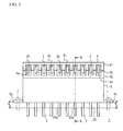
- FIG. 1 is a front view of a connector 1 according to an embodiment.
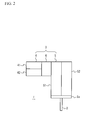
- FIG. 2 is a side view of the connector 1.
- FIG. 3 is a side view of a board 20 on which the connector 1 is mounted.
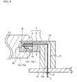
- FIG. 4 is a cross-sectional view taken along line A-A of FIG. 1 .
- the connector 1 includes ten signal pins made of a metal and a housing 3 housing the signal pins 2.
- the housing 3 includes: a front end member 4; a rear end member 5; and an elastic member 6 having a block shape and arranged between the front end member 4 and the rear end member 5.
- the front end member 4 and the elastic member 6 are arranged in series with each other. Further, the rear end member 5 is arranged in a direction perpendicular to the series direction in which the front end member 4 and the elastic member 6 are arranged. Therefore, the side shape of the housing 3 is an L shape, as illustrated in FIG. 2 .
- Each signal pin 2 is bent to correspond to the side shape of the housing 3.
- a bending portion 2a of the signal pin 2 is positioned within the rear end member 5.
- Each signal pin 2 has a terminal 2b at its end. The signal pin 2 is bent to form the terminal 2b.
- the rear end member 5 stands and is secured on one surface of the board 20, as illustrated in FIG. 4 .
- the signal pin 2 is inserted into an attachment hole 20a and is soldered with the other surface of the board 20.
- the rear end member 5 includes flange portions 5a for being secured on the board 20.
- the flange portions 5a are secured on the board 20 with screws.
- the connector 1 is attached in the board 20.
- FIG. 6 is a schematic view of a notebook computer 100 as an example of an electronic device.
- the notebook computer 100 includes a main chassis 101 and a display chassis 102.
- a monitor 102a is installed in the display chassis 102.
- the board 20 is arranged within the main chassis 101.
- a speaker 21 is connected to the board 20.
- an ODD (Optical Disc Drive) 15 and a HDD (Hard Disc Drive) 16 are arranged within the main chassis 101.
- the ODD 15 and the HDD 16 are attached in the main chassis 101.
- the display chassis 102 is connected to the main chassis 101 so as to be openable and closable by means of hinges not illustrated.
- the connector 1 is used to connect the ODD 15 and the board 20, as illustrated in FIG 6 .
- the front end member 4 is connected to a connector 15a provided in the ODD 15.
- the connector 1 is used to connect the HDD 16 and the board 20.
- the front end member 4 is connected to a connector 16a provided in the HDD 16.
- the terminal 2b of the signal pin 2 contacts a terminal 15a1 provided in the ODD 15 to electrically conduct the ODD 15 with the board 20. Further, the terminal 2b of the signal pin 2, a terminal 16a1 of the HDD 16, and the board 20 come into contact with each other to electrically conduct the HDD 16 with the board 20.
- the number of the signal pins 2 provided corresponds to the number of the terminals 15a1 of the ODD 15 and the number of the terminals 16a1 of the HDD 16.
- the front end member 4 is made of a resin and includes a space 4a in its inside.
- the space 4a is defined by every signal pin 2.
- the terminal 2b is housed within the space 4a.
- a resin filled layer 4b is provided within the space 4a.
- the resin filled layer 4b is provided by filling the space 4a with a resin.
- the signal pin 2 is buried by the filling resin to be secured within the front end member 4.
- the rear end member 5 is made of a resin.
- the rear end member 5 is provided with flange portions 5a at a lower portion of its side walls, respectively. As mentioned above, the flange portions 5a are secured on the board 20 with the screws 7.
- the rear end member 5 is provided with spaces 8 in its inside.
- the signal pin 2 can freely move within the space 8.
- the space 8 includes: a first section extending in a direction intersecting the front surface of the board 20, and a second section being continuous with the first section and extending parallel with the front surface of the board 20.
- the space 8 is provided for each signal pin 2.
- the bending portion 2a is positioned within the space 8.
- the space 8 is provided so as not to restrict the relative movement and the bending deformation of the signal pin 2 at the time the rear end member 5 is moved by the vibration of the board 20.
- the elastic member 6 is elastically deformed and the rear end member 5 secured on the board 20 moves relative to the front end member 4.
- the signal pin 2 is soldered with the board 20 and is secured at the front end member 4.
- the signal pin 2 moves relative to the rear end member 5.
- the bending deformation is developed.
- the space 8 permits such a relative movement and such a bending deformation of the signal pin 2.
- the elastic member 6 is made of a rubber material as an example of a elastic material.
- the elastic member 6 has a block shape and can be elastically deformed. Specifically, the elastic member 6 can be deformed in compression deformation, extension deformation, bending deformation, twisting deformation, and a combination thereof. This permits the rear end member 5 to move relative to the front end member 4 upwardly, downwardly, rightwardly, leftwardly, forwardly, and rearwardly.
- a space 9 is defined within the elastic member 6 and the signal pin 2 freely moves within the space 9.
- the space 9 is continuous with the second section of the space 9 of the rear end member 5 and extends in the same direction in which the second section of the space 9 extends.
- the space 9 is provided for each signal pin 2.
- the liner portion of the signal pin 2 is arranged within the space 9.
- the space 9 is provided so as not to restrict the relative movement and the bending deformation of the signal pin 2 at the time the rear end member 5 is moved by the vibration of the board 20.
- the elastic member 6 is deformed.
- the signal pin 2 itself moves with being bent and deformed. Accordingly, the signal pin 2 moves relative to the elastic member 6.
- the space 9 permits such a relative movement and such a bending deformation of the signal pin 2.
- the elastic member 6 is made of a rubber material, the elastic member 6 is deformed by the contact with the signal pin 2. This permits the relative movement of the signal pin 2. For this reason, the space 9 may not be provided. However, the provision of the space 9 permits the signal pin 2 to broadly move.
- the elastic member 6 may be made of a silicon material instead of a rubber material.
- a sponge material may be used instead of a rubber material.
- FIG. 7A is a view of the movement of the signal pin 2 when viewed from its upper.
- FIG. 7B is a view of the movement of the signal pin 2 when viewed from its side.
- the side of the bending portion 2a can move rightwardly and leftwardly.
- the side of the bending portion 2a can move upwardly and downwardly.
- the bending portion 2a can move forwardly and rearwardly.
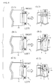
- FIGs. 8 (A-1) to 8(C-2) are explanatory views of the manner where the rightward and leftward vibration of the board 20 secured with the rear end member 5 is absorbed.
- FIG. 8 (A-1) schematically illustrates the connector 1 viewed from its upper side when the board 20 does not vibrate.
- FIG. 8 (A-2) schematically illustrates the signal pin 2 when the board 20 does not vibrate. When the board 20 does not vibrate, the rear end member 5 does not vibrate. Also, the signal pin 2 does not move.
- FIG. 8 (B-1) schematically illustrates the connector 1 viewed from its upper side when the board 20 vibrates rightwardly.
- FIG. 8 (B-2) schematically illustrates the signal pin 2 when the board 20 vibrates rightwardly.
- FIG. 8 (C-1) schematically illustrates the connector 1 viewed from its upper side when the board 20 vibrates leftwardly.
- FIG. 8 (B-2) schematically illustrates the signal pin 2 when the board 20 vibrates leftwardly.
- FIGs. 9A to 9C are explanatory views of the manner where the upward and downward vibration of the board 20 secured with the rear end member 5 is absorbed.
- FIG. 9A schematically illustrates the connector 1 when viewed from its upper side when the board 20 vibrates leftward.
- FIG. 9A also illustrates the signal pin 2.
- the board 20 does not vibrate, the rear end member 5 does not move.
- the signal pin 2 does not move.
- FIG. 9B schematically illustrates the connector 1 when viewed from its side when the board 20 vibrates upwardly.
- FIG. 9B also illustrates the signal pin 2.
- FIG. 9C schematically illustrates the connector 1 when viewed from its side when the board 20 vibrates downwardly.
- FIG. 9C also illustrates the signal pin 2.
- FIGs. 10A to 10C are explanatory views of the manner where the front and rear vibration of the board 20 secured with the rear end member 5 is absorbed.
- FIG. 10A schematically illustrates the connector 1 when viewed from its rear side when the board 20 does not vibrate. Also, FIG. 10A illustrates the signal pin 2. When the board 20 does not vibrate, the rear end member 5 does not move. Also, the signal pin 2 does not move.
- FIG. 10B schematically illustrates the connector 1 when viewed from its side when the board 20 vibrates rearwardly.
- FIG. 10B also illustrates the signal pin 2.
- FIG. 10C schematically illustrates the connector 1 when viewed from its side when the board 20 vibrates frontwardly.
- FIG. 10C also illustrates the signal pin 2.
- the elastic member 6 is elastically deformed so as to follow the movement of the rear end member 5.
- the vibration is restricted from being transmitted to the ODD 15. That is, the elastic deformation of the elastic member 6 restricts the movement of the front end member 4 and the vibration of the ODD 15 connected to the front end member 4.
- the terminal 2b of the signal pin 2 is secured and the vibration of the ODD 15 is restricted, thereby maintaining the stable conduction between the terminals 15a1 and 2b. This result can restrict an error in reading or writing data in the ODD 15.
- the side of the bending portion 2a of the signal pin 2 is permitted to move with the board 20. Moreover, the bending portion 2a is permitted to bend. This can restrict the signal pin 2 from locally receiving a stress. Since the local stress in the signal pin 2 is restricted, damage of the signal pin 2 can be avoided.
- FIG. 11 is an explanatory view of the disassembled housing 3 when viewed from its side.
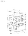
- FIG. 12 is a perspective view of the disassembled housing 3.
- the front end member 4 and the rear end member 5 are provided in the housing 3 of the connector 1. Further, the elastic member 6 having a block shape is provided between the front end member 4 and the rear end member 5.
- the front end member 4 is divided into an upper member 41 and a lower member 42.
- the rear end member 5 is divided into a front member 51 and a rear member 52.
- the upper member 41 has grooves 41 a.
- the groove 41 a is provided for each signal pin 2.
- the groove 41a is provided with a resin filled layer 4b.
- the lower member 42 has grooves 42a.
- the groove 42a is provided for each signal pin 2.
- the grooves 41 a and 42a define the space 4a when the housing 3 is assembled.
- FIG. 13 is a cross-sectional view of the upper member 41 within which the signal pin 2 is arranged and which is filled with the resin.
- the signal pin 2 is secured on the upper member 41 by the resin filled layer 4b formed within the upper member 41. After this, the end portion of the signal pin 2 is bent to provide the terminal 2b. Additionally, the bending for providing the signal pin 2 may be performed later.
- the signal pin 2 is secured in the upper member 41 with the resin filled layer 4b, the upper member 41 and the lower member 42 are jointed by bonding. Therefore, the front end member 4 is formed.
- the elastic member 6 beforehand prepared and the front end member 4 are jointed by bonding.
- the elastic member 6 is beforehand provided with the space 9 for each signal pin 2. Before the elastic member 6 and the front end member 4 are jointed, first, the signal pin 2 is penetrated though the space 9. Next, the elastic member 6 and the front end member 4 are jointed.
- the front member 51 After the jointing of the elastic member 6 with the front end member 4 is accomplished, the front member 51 beforehand prepared and the elastic member 6 are jointed by bonding.
- the front member 51 is beforehand provided with grooves 51a and grooves 51b respectively continuous with the grooves 51a.
- the groove 51a is continuous with the space 9 of the elastic member 6.
- the groove 51b extends in a direction perpendicular to the direction of the groove 51a.
- the groove 51a defines the space 8 within the rear end member 5 in conjunction with a groove 52a, as will be described later.
- the signal pin 2 is penetrated through the front member 51.
- the elastic member 6 and the front member 51 are jointed.
- the elastic member 6 and the front end member 4 may be jointed after the elastic member 6 and the front member 51 are jointed.
- the bending portion 2a of the signal pin 2 is formed, after accomplishing the jointing of three members, specifically, the front end member 4, the elastic member 6, and the front member 51.
- the bending portion 2a is formed by bending the signal pin 2 in the direction toward which the groove 51b extends. That is, the signal pin 2 is bent at the bending portion 2a by 90 degrees.
- the rear member 52 After the bending portion 2a is formed in the signal pin 2, the rear member 52 beforehand prepared and the front member 51 are jointed by bonding.
- the rear member 52 is beforehand provided with the grooves 52a.
- the groove 52a defines the space 8 in conjunction with the groove 51b. Further, the flange portion 5a is continuously provided at the lower edge of the rear member 52.
- the rear end member 5 By jointing the front member 51 with the rear member 52, the rear end member 5 is formed.
- the space 8 is defined within the rear end member 5, and houses the signal pin 2.
- FIG. 14 is a cross-sectional view of the front end member 45.
- the signal pin 2 is integrally formed in the front end member 45 from the beginning of the formation and is fixed. For this reason, the front end member 45 does not need the resin filled layer 4b, in contrast to the front end member 4. Further, the front end member 45 is not divided into two members, in contrast to the front end member 4. That is, the entire front end member 45 is formed by plastic molding.
- the bonding is used for jointing the members.
- other methods may joint the members.
- the jointing may be ensured by a claw 61 and a receiving portion 62 fitted onto the claw 61 as illustrated in FIG. 15.
- FIG. 15 illustrates an example of the receiving portion 62 formed in the upper member 41 defining the front end member 4, and the claw 61 formed in the lower member 42.
- the upper member 41 and the lower member 42 can be jointed by fitting the claw 61 into the receiving portion 62.
- other members can be jointed.
- the flange portions 5a are secured by the screws 7, whereby the connector 1 formed as mentioned above is attached to the board 20.
- each of the signal pin 2 is inserted into the attachment hole 20a provided in the board 20.
- a jig 70 for positioning the signal pin 2 can be used.
- the jig 70 has plural grooves 70a and has a comb shape.
- the signal pin 2 is not secured within the space 8 provided in the rear end member 5. For this reason, the free end of the signal pin 2 inserted into the attachment hole 20a might vibrate and the position thereof might be stable. Thus, the free end of each signal pin 2 is supported within the grooves 70a of the jig 70 and is them positioned.
- the free end is inserted into the attachment hole 20a with the free end of each signal pin 2 supported by the jig 70. Then, the jig 70 is pulled toward its side. Successively, the signal pin 2 is further inserted. After this, the back side of the board 20 is soldered to attach the connector 1 on the board 20. In the drawing, the numerous number 22 depicts the solder.
- FIG. 17 is a cross-sectional view of the connector 1.
- the resin filled layer 72 is provided within the space 8 at the lower edge of the rear end member 5.
- This resin filled layer 72 supports the free end of the signal pin 2. This facilitates the positioning of the signal pin 2. Consequently, the jig 70 is not needed. Additionally, the resin filled layer 72 may be provided within all of the spaces 8, or only within a part of the space 8.
- the board 20 attached with the connector 1 is arranged within the main chassis 101 of the notebook computer 100.
- the board 20 is connected to the ODD 15 via the connector 1.
- the board 20 is connected to the ODD 15 via the connector 1.
- the board 20 might vibrate. Even when such vibration of the board 20 is generated, the connector 1 absorbs the vibration in the manner mentioned above. Thus, the transmission of the vibration to the ODD 15 is restricted. Consequently, the transmission of the vibration of the head of the ODD 15 is restricted. Further, the terminal 2b of the signal pin 2 is secured in the front end member 4 and the vibration of the ODD 15 is restricted, whereby the electrical conduction between the terminals 15a1 and 2b are stably maintained. This result restricts an error in reading or writing data in the ODD 15. Also, this result restricts an error in reading or writing data in the HDD 16 is restricted.
- the reason why the board 20 vibrates has another factor such as falling of the notebook computer 100 or the vibration thereof in addition to the use of the speaker 21. Even when the vibration of the board 20 is generated due to another factor, the connector 1 according to the present embodiment can restrict an error in reading or writing data in the ODD 15 or in the HDD 16.
- the ODD 15 and the HDD 16 are exemplified as an electronic component.
- the connector 1 can be used for electrically conducting the board and another type of electronic component such as a Personal Computer Memory Card International Association (PCMCIA) card. Even in cases where the connector is used for such another type of electronic component, the electrical conduction between the board and the electronic component is also stably maintained.
- PCMCIA Personal Computer Memory Card International Association
- the materials of the elastic member and the signal pin can be varied in light of the application of the connector.
- the material of the signal pin can be decided in light of its electrical conductivity or its elasticity.
- the personal computer is exemplified as an electronic device.
- the connector 1 is applicable for another electronic device such as a DVD player, an audio player providing with a HDD, and the like.
Landscapes
- Engineering & Computer Science (AREA)
- Theoretical Computer Science (AREA)
- Computer Hardware Design (AREA)
- Power Engineering (AREA)
- Human Computer Interaction (AREA)
- Physics & Mathematics (AREA)
- General Engineering & Computer Science (AREA)
- General Physics & Mathematics (AREA)
- Coupling Device And Connection With Printed Circuit (AREA)
- Details Of Connecting Devices For Male And Female Coupling (AREA)
- Connector Housings Or Holding Contact Members (AREA)
Claims (6)
- Eine Verbindungseinheit (1), umfassend:einen Signalpin (2), an einer Stirnseite davon mit einem Anschluss (2b) versehen, ausgebildet zum Kontaktieren eines in einem elektronischen Bauelement (15, 16) vorgesehenen Anschlusses (15a1,16a1), und zum elektrischen Verbinden einer Platine (20) mit dem elektronischen Bauelement (15, 16); undein Gehäuse (3) zum Aufnehmen des Signalpins (2),wobei das Gehäuse (3) umfasst:ein Stirnseitenelement (4), innerhalb welchem der Signalpin (2) befestigt ist, und welches mit einer in dem elektronischen Bauelement (15, 16) vorgesehenen Verbindungseinheit (15a, 16a) verbindbar ist;ein Rückseitenelement (5), befestigbar in der Platine (20); undein elastisches Element (6), welches zwischen dem Stirnseitenelement (4) und dem Rückseitenelement (5) angeordnet ist und eine Blockform aufweist;dadurch gekennzeichnet, dass:das Rückseitenelement (5) eine Aussparung (8) dazwischen definiert, wobei der Signalpin (2) nicht innerhalb der in dem Rückseitenelement (5) vorgesehenen Aussparung (8) befestigt ist, sodass der Signalpin (2) innerhalb der Aussparung (8) frei beweglich ist, unddas elastische Element (6) eine Aussparung (9) dazwischen definiert, wobei der Signalpin (2) innerhalb der Aussparung (9) frei beweglich ist, wobeidie Aussparung (8) des Rückseitenelements (5) umfasst:eine erste Sektion, welche sich in einer eine Oberfläche der Platine (20) schneidenden Richtung erstreckt; undeine zweite Sektion, welche durchgehend mit der ersten Sektion ist und sich in einer Richtung quer zu der Richtung erstreckt, in welcher sich die erste Sektion erstreckt, undwobei die Aussparung (9) des elastischen Elements (6) mit der zweiten Sektion des Rückseitenelements (5) durchgehend ist und sich in einer Richtung identisch zu der Richtung erstreckt, in welcher sich die zweite Sektion erstreckt.
- Verbindungseinheit (1) aus Anspruch 1, dadurch gekennzeichnet, dass das elastische Element (6) aus Gummi, Silikon oder Schwammmaterial gefertigt ist.
- Eine elektronische Vorrichtung, umfassend:ein elektronisches Bauelement (15, 16), welches mit der Verbindungseinheit (1) aus Anspruch 1 oder Anspruch 2 verbunden ist; undeine Platine (20), welche durch die Verbindungseinheit (1) in elektrischer Verbindung mit dem elektronischen Bauelement (15, 16) ist.
- Die elektronische Vorrichtung aus Anspruch 3, weiter umfassend ein Chassis (101), welches das elektronische Bauelement (15, 16) und die Platine (20) aufnimmt.
- Die elektronische Vorrichtung aus Anspruch 3 oder Anspruch 4, dadurch gekennzeichnet, dass die elektronische Komponente (15, 16) eine Speichervorrichtung ist, welche auf ein durch einen Rotationsmechanismus rotiertes Speichermedium zugreift und Daten von dem Speichermedium ausliest oder darauf schreibt.
- Die elektronische Vorrichtung nach einem der Ansprüche 3 bis 5, weiter umfassend ein weiteres elektronisches Bauelement (23), welches innerhalb des Chassis (101) aufgenommen ist und welches bei Verwendung vibriert.
Applications Claiming Priority (1)
| Application Number | Priority Date | Filing Date | Title |
|---|---|---|---|
| PCT/JP2008/061836 WO2010001450A1 (ja) | 2008-06-30 | 2008-06-30 | コネクタ並びにこれを備えた基板及び電子機器 |
Publications (3)
| Publication Number | Publication Date |
|---|---|
| EP2302742A1 EP2302742A1 (de) | 2011-03-30 |
| EP2302742A4 EP2302742A4 (de) | 2011-11-16 |
| EP2302742B1 true EP2302742B1 (de) | 2015-09-02 |
Family
ID=41465566
Family Applications (1)
| Application Number | Title | Priority Date | Filing Date |
|---|---|---|---|
| EP08790749.9A Not-in-force EP2302742B1 (de) | 2008-06-30 | 2008-06-30 | Verbinder, substrat damit und elektronische anordnung |
Country Status (6)
| Country | Link |
|---|---|
| US (1) | US8033851B2 (de) |
| EP (1) | EP2302742B1 (de) |
| JP (1) | JP5126361B2 (de) |
| KR (1) | KR101193574B1 (de) |
| CN (1) | CN102077426B (de) |
| WO (1) | WO2010001450A1 (de) |
Families Citing this family (8)
| Publication number | Priority date | Publication date | Assignee | Title |
|---|---|---|---|---|
| JP5033144B2 (ja) * | 2009-01-20 | 2012-09-26 | Toa株式会社 | ユニット式電子機器 |
| JP5923253B2 (ja) * | 2011-08-01 | 2016-05-24 | 矢崎総業株式会社 | 圧接端子固定構造 |
| JP5975326B2 (ja) * | 2012-03-01 | 2016-08-23 | 日本電気株式会社 | コネクタ構造及び電子装置 |
| DE202013006067U1 (de) * | 2013-07-05 | 2013-08-12 | Rosenberger Hochfrequenztechnik Gmbh & Co. Kg | Steckverbinder |
| DE102017002853A1 (de) | 2017-03-23 | 2018-09-27 | Yamaichi Electronics Deutschland Gmbh | Schalthebelbaugruppe |
| CN209744330U (zh) * | 2019-04-17 | 2019-12-06 | 漳州立达信灯具有限公司 | 一种柔性灯体拼接件 |
| JP7321878B2 (ja) * | 2019-10-15 | 2023-08-07 | ヒロセ電機株式会社 | コネクタ |
| JP2022188680A (ja) * | 2021-06-09 | 2022-12-21 | イリソ電子工業株式会社 | フローティングコネクタ |
Family Cites Families (17)
| Publication number | Priority date | Publication date | Assignee | Title |
|---|---|---|---|---|
| JP2831382B2 (ja) | 1988-12-15 | 1998-12-02 | 三井化学株式会社 | 2、3―ジヒドロベンゾフラン誘導体及びこれらを有効成分とする除草剤 |
| JPH051914Y2 (de) * | 1989-06-09 | 1993-01-19 | ||
| JP3016164B2 (ja) * | 1991-06-19 | 2000-03-06 | 日本エー・エム・ピー株式会社 | 可動型コネクタ |
| JPH0531158A (ja) | 1991-07-31 | 1993-02-09 | Morita Mfg Co Ltd | 医科・歯科用診療機材 |
| JPH0531158U (ja) | 1991-09-25 | 1993-04-23 | 株式会社カンセイ | 電気コネクタ |
| EP0625810B1 (de) * | 1993-05-20 | 1999-01-20 | Sumitomo Wiring Systems, Ltd. | Elektrischer Steckverbinder |
| JP3166119B2 (ja) * | 1996-02-16 | 2001-05-14 | 矢崎総業株式会社 | 基板用可動コネクタ及びコネクタ端子 |
| JP4183102B2 (ja) * | 1996-11-11 | 2008-11-19 | ソニー株式会社 | プラグコネクタ |
| JP2001326037A (ja) * | 2000-05-16 | 2001-11-22 | Tokai Rika Co Ltd | プリント配線板用コネクタ装置 |
| JP2001332358A (ja) * | 2000-05-19 | 2001-11-30 | Tokai Rika Co Ltd | コネクタ装置 |
| JP4265892B2 (ja) * | 2002-08-06 | 2009-05-20 | インターナショナル・ビジネス・マシーンズ・コーポレーション | コネクタ装置 |
| JP4356548B2 (ja) * | 2004-07-20 | 2009-11-04 | 住友電装株式会社 | 基板用コネクタ |
| JP2006338970A (ja) * | 2005-05-31 | 2006-12-14 | Toshiba Corp | コネクタ装置、回路基板、電子機器 |
| JP4665848B2 (ja) * | 2006-03-15 | 2011-04-06 | 日立電線株式会社 | コネクタ構造 |
| US7530830B1 (en) * | 2007-07-19 | 2009-05-12 | Sunpower Corporation | Misalignment tolerant connector |
| CN201142419Y (zh) * | 2007-10-26 | 2008-10-29 | 实盈电子(东莞)有限公司 | 连接器防震结构 |
| US7766684B2 (en) * | 2008-02-22 | 2010-08-03 | International Business Machines Corporation | Connector actuation mechanism |
-
2008
- 2008-06-30 EP EP08790749.9A patent/EP2302742B1/de not_active Not-in-force
- 2008-06-30 KR KR1020107029260A patent/KR101193574B1/ko not_active Expired - Fee Related
- 2008-06-30 CN CN200880130104.7A patent/CN102077426B/zh not_active Expired - Fee Related
- 2008-06-30 WO PCT/JP2008/061836 patent/WO2010001450A1/ja not_active Ceased
- 2008-06-30 JP JP2010518836A patent/JP5126361B2/ja not_active Expired - Fee Related
-
2010
- 2010-12-14 US US12/967,376 patent/US8033851B2/en not_active Expired - Fee Related
Also Published As
| Publication number | Publication date |
|---|---|
| EP2302742A4 (de) | 2011-11-16 |
| US20110081792A1 (en) | 2011-04-07 |
| CN102077426A (zh) | 2011-05-25 |
| US8033851B2 (en) | 2011-10-11 |
| EP2302742A1 (de) | 2011-03-30 |
| JP5126361B2 (ja) | 2013-01-23 |
| WO2010001450A1 (ja) | 2010-01-07 |
| KR101193574B1 (ko) | 2012-10-23 |
| KR20110028593A (ko) | 2011-03-21 |
| CN102077426B (zh) | 2013-07-03 |
| JPWO2010001450A1 (ja) | 2011-12-15 |
Similar Documents
| Publication | Publication Date | Title |
|---|---|---|
| EP2302742B1 (de) | Verbinder, substrat damit und elektronische anordnung | |
| US6595786B2 (en) | Electrical connecting structure of mounted part, computer apparatus, and electronic equipment | |
| CN103872542B (zh) | 具有防水与避振功能的连接器的电子装置 | |
| CN108633163B (zh) | 用于电子装置的电路板的避震结构及其电子装置 | |
| CN101364133B (zh) | 电子部件安装构件及电子装置 | |
| US20080024972A1 (en) | Buffer member | |
| WO2007119814A1 (ja) | 光伝送モジュール、接続部品、および光伝送モジュールを備えた電子機器 | |
| US7215506B2 (en) | Hard disk drive (HDD) assembly of small form-factor HDD shock-mounted in frame having dimensions of larger form-factor HDD | |
| US7688575B2 (en) | Display device and information processing apparatus | |
| US20080057781A1 (en) | Mounting assembly for connectors | |
| CN201170866Y (zh) | 固定件 | |
| EP2474876A1 (de) | Elektronische vorrichtung | |
| JP3544937B2 (ja) | ディスク挿抜装置 | |
| JP4221725B2 (ja) | ハードディスク接続コネクタ | |
| JP5434952B2 (ja) | データカートリッジ装置 | |
| JP4487099B2 (ja) | データ記録装置の接続ユニット | |
| KR101014023B1 (ko) | 자동차용 미니 비 타입 유에스비 커넥터 | |
| US8526141B2 (en) | Magnetic disk device and guide member for guiding a flexible wiring board | |
| JP4412553B2 (ja) | 光ピックアップ装置 | |
| KR101417021B1 (ko) | 광 픽업 장착장치 및 광 픽업이 장착된 노트북 컴퓨터 | |
| JP2008152895A (ja) | ハードディスク内蔵dvdレコーダ及びハードディスクユニットの取付構造 | |
| JP2010108573A (ja) | 光ディスク装置及びその製造方法 | |
| JP2010210787A (ja) | 表示装置 | |
| JP2004006543A (ja) | 電子機器の筐体構造 | |
| JP2007234357A (ja) | カードコネクタ装置、および電子機器 |
Legal Events
| Date | Code | Title | Description |
|---|---|---|---|
| PUAI | Public reference made under article 153(3) epc to a published international application that has entered the european phase |
Free format text: ORIGINAL CODE: 0009012 |
|
| 17P | Request for examination filed |
Effective date: 20110124 |
|
| AK | Designated contracting states |
Kind code of ref document: A1 Designated state(s): AT BE BG CH CY CZ DE DK EE ES FI FR GB GR HR HU IE IS IT LI LT LU LV MC MT NL NO PL PT RO SE SI SK TR |
|
| AX | Request for extension of the european patent |
Extension state: AL BA MK RS |
|
| DAX | Request for extension of the european patent (deleted) | ||
| A4 | Supplementary search report drawn up and despatched |
Effective date: 20111018 |
|
| RIC1 | Information provided on ipc code assigned before grant |
Ipc: H01R 13/631 20060101ALI20111012BHEP Ipc: H01R 12/72 20110101ALI20111012BHEP Ipc: H01R 13/533 20060101AFI20111012BHEP |
|
| 17Q | First examination report despatched |
Effective date: 20130328 |
|
| REG | Reference to a national code |
Ref country code: DE Ref legal event code: R079 Ref document number: 602008039969 Country of ref document: DE Free format text: PREVIOUS MAIN CLASS: H01R0013533000 Ipc: G06F0001180000 |
|
| GRAP | Despatch of communication of intention to grant a patent |
Free format text: ORIGINAL CODE: EPIDOSNIGR1 |
|
| RIC1 | Information provided on ipc code assigned before grant |
Ipc: H01R 13/533 20060101ALI20150218BHEP Ipc: G11B 33/08 20060101ALI20150218BHEP Ipc: H01R 12/72 20110101ALI20150218BHEP Ipc: G06F 1/18 20060101AFI20150218BHEP Ipc: H01R 13/502 20060101ALI20150218BHEP Ipc: H01R 13/631 20060101ALI20150218BHEP |
|
| INTG | Intention to grant announced |
Effective date: 20150323 |
|
| GRAS | Grant fee paid |
Free format text: ORIGINAL CODE: EPIDOSNIGR3 |
|
| GRAA | (expected) grant |
Free format text: ORIGINAL CODE: 0009210 |
|
| AK | Designated contracting states |
Kind code of ref document: B1 Designated state(s): AT BE BG CH CY CZ DE DK EE ES FI FR GB GR HR HU IE IS IT LI LT LU LV MC MT NL NO PL PT RO SE SI SK TR |
|
| REG | Reference to a national code |
Ref country code: GB Ref legal event code: FG4D |
|
| REG | Reference to a national code |
Ref country code: AT Ref legal event code: REF Ref document number: 747010 Country of ref document: AT Kind code of ref document: T Effective date: 20150915 Ref country code: CH Ref legal event code: EP |
|
| REG | Reference to a national code |
Ref country code: IE Ref legal event code: FG4D |
|
| REG | Reference to a national code |
Ref country code: DE Ref legal event code: R096 Ref document number: 602008039969 Country of ref document: DE |
|
| REG | Reference to a national code |
Ref country code: AT Ref legal event code: MK05 Ref document number: 747010 Country of ref document: AT Kind code of ref document: T Effective date: 20150902 |
|
| PG25 | Lapsed in a contracting state [announced via postgrant information from national office to epo] |
Ref country code: NO Free format text: LAPSE BECAUSE OF FAILURE TO SUBMIT A TRANSLATION OF THE DESCRIPTION OR TO PAY THE FEE WITHIN THE PRESCRIBED TIME-LIMIT Effective date: 20151202 Ref country code: LT Free format text: LAPSE BECAUSE OF FAILURE TO SUBMIT A TRANSLATION OF THE DESCRIPTION OR TO PAY THE FEE WITHIN THE PRESCRIBED TIME-LIMIT Effective date: 20150902 Ref country code: LV Free format text: LAPSE BECAUSE OF FAILURE TO SUBMIT A TRANSLATION OF THE DESCRIPTION OR TO PAY THE FEE WITHIN THE PRESCRIBED TIME-LIMIT Effective date: 20150902 Ref country code: FI Free format text: LAPSE BECAUSE OF FAILURE TO SUBMIT A TRANSLATION OF THE DESCRIPTION OR TO PAY THE FEE WITHIN THE PRESCRIBED TIME-LIMIT Effective date: 20150902 Ref country code: GR Free format text: LAPSE BECAUSE OF FAILURE TO SUBMIT A TRANSLATION OF THE DESCRIPTION OR TO PAY THE FEE WITHIN THE PRESCRIBED TIME-LIMIT Effective date: 20151203 |
|
| REG | Reference to a national code |
Ref country code: LT Ref legal event code: MG4D Ref country code: NL Ref legal event code: MP Effective date: 20150902 |
|
| PG25 | Lapsed in a contracting state [announced via postgrant information from national office to epo] |
Ref country code: AT Free format text: LAPSE BECAUSE OF FAILURE TO SUBMIT A TRANSLATION OF THE DESCRIPTION OR TO PAY THE FEE WITHIN THE PRESCRIBED TIME-LIMIT Effective date: 20150902 Ref country code: SE Free format text: LAPSE BECAUSE OF FAILURE TO SUBMIT A TRANSLATION OF THE DESCRIPTION OR TO PAY THE FEE WITHIN THE PRESCRIBED TIME-LIMIT Effective date: 20150902 Ref country code: ES Free format text: LAPSE BECAUSE OF FAILURE TO SUBMIT A TRANSLATION OF THE DESCRIPTION OR TO PAY THE FEE WITHIN THE PRESCRIBED TIME-LIMIT Effective date: 20150902 Ref country code: PL Free format text: LAPSE BECAUSE OF FAILURE TO SUBMIT A TRANSLATION OF THE DESCRIPTION OR TO PAY THE FEE WITHIN THE PRESCRIBED TIME-LIMIT Effective date: 20150902 |
|
| PG25 | Lapsed in a contracting state [announced via postgrant information from national office to epo] |
Ref country code: SK Free format text: LAPSE BECAUSE OF FAILURE TO SUBMIT A TRANSLATION OF THE DESCRIPTION OR TO PAY THE FEE WITHIN THE PRESCRIBED TIME-LIMIT Effective date: 20150902 Ref country code: IT Free format text: LAPSE BECAUSE OF FAILURE TO SUBMIT A TRANSLATION OF THE DESCRIPTION OR TO PAY THE FEE WITHIN THE PRESCRIBED TIME-LIMIT Effective date: 20150902 Ref country code: IS Free format text: LAPSE BECAUSE OF FAILURE TO SUBMIT A TRANSLATION OF THE DESCRIPTION OR TO PAY THE FEE WITHIN THE PRESCRIBED TIME-LIMIT Effective date: 20160102 Ref country code: CZ Free format text: LAPSE BECAUSE OF FAILURE TO SUBMIT A TRANSLATION OF THE DESCRIPTION OR TO PAY THE FEE WITHIN THE PRESCRIBED TIME-LIMIT Effective date: 20150902 Ref country code: NL Free format text: LAPSE BECAUSE OF FAILURE TO SUBMIT A TRANSLATION OF THE DESCRIPTION OR TO PAY THE FEE WITHIN THE PRESCRIBED TIME-LIMIT Effective date: 20150902 Ref country code: EE Free format text: LAPSE BECAUSE OF FAILURE TO SUBMIT A TRANSLATION OF THE DESCRIPTION OR TO PAY THE FEE WITHIN THE PRESCRIBED TIME-LIMIT Effective date: 20150902 |
|
| PG25 | Lapsed in a contracting state [announced via postgrant information from national office to epo] |
Ref country code: PT Free format text: LAPSE BECAUSE OF FAILURE TO SUBMIT A TRANSLATION OF THE DESCRIPTION OR TO PAY THE FEE WITHIN THE PRESCRIBED TIME-LIMIT Effective date: 20160104 Ref country code: RO Free format text: LAPSE BECAUSE OF FAILURE TO SUBMIT A TRANSLATION OF THE DESCRIPTION OR TO PAY THE FEE WITHIN THE PRESCRIBED TIME-LIMIT Effective date: 20150902 |
|
| REG | Reference to a national code |
Ref country code: FR Ref legal event code: PLFP Year of fee payment: 9 Ref country code: DE Ref legal event code: R097 Ref document number: 602008039969 Country of ref document: DE |
|
| PLBE | No opposition filed within time limit |
Free format text: ORIGINAL CODE: 0009261 |
|
| STAA | Information on the status of an ep patent application or granted ep patent |
Free format text: STATUS: NO OPPOSITION FILED WITHIN TIME LIMIT |
|
| 26N | No opposition filed |
Effective date: 20160603 |
|
| PG25 | Lapsed in a contracting state [announced via postgrant information from national office to epo] |
Ref country code: DK Free format text: LAPSE BECAUSE OF FAILURE TO SUBMIT A TRANSLATION OF THE DESCRIPTION OR TO PAY THE FEE WITHIN THE PRESCRIBED TIME-LIMIT Effective date: 20150902 Ref country code: SI Free format text: LAPSE BECAUSE OF FAILURE TO SUBMIT A TRANSLATION OF THE DESCRIPTION OR TO PAY THE FEE WITHIN THE PRESCRIBED TIME-LIMIT Effective date: 20150902 |
|
| PG25 | Lapsed in a contracting state [announced via postgrant information from national office to epo] |
Ref country code: BE Free format text: LAPSE BECAUSE OF FAILURE TO SUBMIT A TRANSLATION OF THE DESCRIPTION OR TO PAY THE FEE WITHIN THE PRESCRIBED TIME-LIMIT Effective date: 20150902 |
|
| PG25 | Lapsed in a contracting state [announced via postgrant information from national office to epo] |
Ref country code: MC Free format text: LAPSE BECAUSE OF FAILURE TO SUBMIT A TRANSLATION OF THE DESCRIPTION OR TO PAY THE FEE WITHIN THE PRESCRIBED TIME-LIMIT Effective date: 20150902 |
|
| REG | Reference to a national code |
Ref country code: CH Ref legal event code: PL |
|
| REG | Reference to a national code |
Ref country code: IE Ref legal event code: MM4A |
|
| PG25 | Lapsed in a contracting state [announced via postgrant information from national office to epo] |
Ref country code: LI Free format text: LAPSE BECAUSE OF NON-PAYMENT OF DUE FEES Effective date: 20160630 Ref country code: CH Free format text: LAPSE BECAUSE OF NON-PAYMENT OF DUE FEES Effective date: 20160630 |
|
| REG | Reference to a national code |
Ref country code: FR Ref legal event code: PLFP Year of fee payment: 10 |
|
| PG25 | Lapsed in a contracting state [announced via postgrant information from national office to epo] |
Ref country code: IE Free format text: LAPSE BECAUSE OF NON-PAYMENT OF DUE FEES Effective date: 20160630 |
|
| REG | Reference to a national code |
Ref country code: FR Ref legal event code: PLFP Year of fee payment: 11 |
|
| PG25 | Lapsed in a contracting state [announced via postgrant information from national office to epo] |
Ref country code: HU Free format text: LAPSE BECAUSE OF FAILURE TO SUBMIT A TRANSLATION OF THE DESCRIPTION OR TO PAY THE FEE WITHIN THE PRESCRIBED TIME-LIMIT; INVALID AB INITIO Effective date: 20080630 Ref country code: CY Free format text: LAPSE BECAUSE OF FAILURE TO SUBMIT A TRANSLATION OF THE DESCRIPTION OR TO PAY THE FEE WITHIN THE PRESCRIBED TIME-LIMIT Effective date: 20150902 |
|
| PG25 | Lapsed in a contracting state [announced via postgrant information from national office to epo] |
Ref country code: LU Free format text: LAPSE BECAUSE OF NON-PAYMENT OF DUE FEES Effective date: 20160630 Ref country code: HR Free format text: LAPSE BECAUSE OF FAILURE TO SUBMIT A TRANSLATION OF THE DESCRIPTION OR TO PAY THE FEE WITHIN THE PRESCRIBED TIME-LIMIT Effective date: 20150902 Ref country code: TR Free format text: LAPSE BECAUSE OF FAILURE TO SUBMIT A TRANSLATION OF THE DESCRIPTION OR TO PAY THE FEE WITHIN THE PRESCRIBED TIME-LIMIT Effective date: 20150902 Ref country code: MT Free format text: LAPSE BECAUSE OF NON-PAYMENT OF DUE FEES Effective date: 20160630 |
|
| PG25 | Lapsed in a contracting state [announced via postgrant information from national office to epo] |
Ref country code: BG Free format text: LAPSE BECAUSE OF FAILURE TO SUBMIT A TRANSLATION OF THE DESCRIPTION OR TO PAY THE FEE WITHIN THE PRESCRIBED TIME-LIMIT Effective date: 20150902 |
|
| PGFP | Annual fee paid to national office [announced via postgrant information from national office to epo] |
Ref country code: DE Payment date: 20180619 Year of fee payment: 11 |
|
| PGFP | Annual fee paid to national office [announced via postgrant information from national office to epo] |
Ref country code: FR Payment date: 20180511 Year of fee payment: 11 |
|
| PGFP | Annual fee paid to national office [announced via postgrant information from national office to epo] |
Ref country code: GB Payment date: 20180627 Year of fee payment: 11 |
|
| REG | Reference to a national code |
Ref country code: DE Ref legal event code: R081 Ref document number: 602008039969 Country of ref document: DE Owner name: FUJITSU CLIENT COMPUTING LIMITED, KAWASAKI-SHI, JP Free format text: FORMER OWNER: FUJITSU LTD., KAWASAKI-SHI, KANAGAWA, JP Ref country code: DE Ref legal event code: R082 Ref document number: 602008039969 Country of ref document: DE Representative=s name: HOFFMANN - EITLE PATENT- UND RECHTSANWAELTE PA, DE |
|
| REG | Reference to a national code |
Ref country code: GB Ref legal event code: 732E Free format text: REGISTERED BETWEEN 20190207 AND 20190213 |
|
| REG | Reference to a national code |
Ref country code: DE Ref legal event code: R119 Ref document number: 602008039969 Country of ref document: DE |
|
| GBPC | Gb: european patent ceased through non-payment of renewal fee |
Effective date: 20190630 |
|
| PG25 | Lapsed in a contracting state [announced via postgrant information from national office to epo] |
Ref country code: GB Free format text: LAPSE BECAUSE OF NON-PAYMENT OF DUE FEES Effective date: 20190630 Ref country code: DE Free format text: LAPSE BECAUSE OF NON-PAYMENT OF DUE FEES Effective date: 20200101 |
|
| PG25 | Lapsed in a contracting state [announced via postgrant information from national office to epo] |
Ref country code: FR Free format text: LAPSE BECAUSE OF NON-PAYMENT OF DUE FEES Effective date: 20190630 |