EP2289076B1 - Elektrische bauelementanordnung - Google Patents
Elektrische bauelementanordnung Download PDFInfo
- Publication number
- EP2289076B1 EP2289076B1 EP09749927.1A EP09749927A EP2289076B1 EP 2289076 B1 EP2289076 B1 EP 2289076B1 EP 09749927 A EP09749927 A EP 09749927A EP 2289076 B1 EP2289076 B1 EP 2289076B1
- Authority
- EP
- European Patent Office
- Prior art keywords
- varistor body
- varistor
- arrangement according
- component
- component arrangement
- Prior art date
- Legal status (The legal status is an assumption and is not a legal conclusion. Google has not performed a legal analysis and makes no representation as to the accuracy of the status listed.)
- Not-in-force
Links
Images


Classifications
-
- H—ELECTRICITY
- H01—ELECTRIC ELEMENTS
- H01C—RESISTORS
- H01C7/00—Non-adjustable resistors formed as one or more layers or coatings; Non-adjustable resistors made from powdered conducting material or powdered semi-conducting material with or without insulating material
- H01C7/10—Non-adjustable resistors formed as one or more layers or coatings; Non-adjustable resistors made from powdered conducting material or powdered semi-conducting material with or without insulating material voltage responsive, i.e. varistors
- H01C7/12—Overvoltage protection resistors; Arresters
-
- H—ELECTRICITY
- H01—ELECTRIC ELEMENTS
- H01C—RESISTORS
- H01C7/00—Non-adjustable resistors formed as one or more layers or coatings; Non-adjustable resistors made from powdered conducting material or powdered semi-conducting material with or without insulating material
- H01C7/10—Non-adjustable resistors formed as one or more layers or coatings; Non-adjustable resistors made from powdered conducting material or powdered semi-conducting material with or without insulating material voltage responsive, i.e. varistors
- H01C7/102—Varistor boundary, e.g. surface layers
-
- H—ELECTRICITY
- H01—ELECTRIC ELEMENTS
- H01C—RESISTORS
- H01C7/00—Non-adjustable resistors formed as one or more layers or coatings; Non-adjustable resistors made from powdered conducting material or powdered semi-conducting material with or without insulating material
- H01C7/10—Non-adjustable resistors formed as one or more layers or coatings; Non-adjustable resistors made from powdered conducting material or powdered semi-conducting material with or without insulating material voltage responsive, i.e. varistors
- H01C7/105—Varistor cores
-
- H—ELECTRICITY
- H10—SEMICONDUCTOR DEVICES; ELECTRIC SOLID-STATE DEVICES NOT OTHERWISE PROVIDED FOR
- H10W—GENERIC PACKAGES, INTERCONNECTIONS, CONNECTORS OR OTHER CONSTRUCTIONAL DETAILS OF DEVICES COVERED BY CLASS H10
- H10W72/00—Interconnections or connectors in packages
- H10W72/50—Bond wires
- H10W72/531—Shapes of wire connectors
- H10W72/536—Shapes of wire connectors the connected ends being ball-shaped
-
- H—ELECTRICITY
- H10—SEMICONDUCTOR DEVICES; ELECTRIC SOLID-STATE DEVICES NOT OTHERWISE PROVIDED FOR
- H10W—GENERIC PACKAGES, INTERCONNECTIONS, CONNECTORS OR OTHER CONSTRUCTIONAL DETAILS OF DEVICES COVERED BY CLASS H10
- H10W72/00—Interconnections or connectors in packages
- H10W72/50—Bond wires
- H10W72/531—Shapes of wire connectors
- H10W72/5363—Shapes of wire connectors the connected ends being wedge-shaped
-
- H—ELECTRICITY
- H10—SEMICONDUCTOR DEVICES; ELECTRIC SOLID-STATE DEVICES NOT OTHERWISE PROVIDED FOR
- H10W—GENERIC PACKAGES, INTERCONNECTIONS, CONNECTORS OR OTHER CONSTRUCTIONAL DETAILS OF DEVICES COVERED BY CLASS H10
- H10W72/00—Interconnections or connectors in packages
- H10W72/50—Bond wires
- H10W72/541—Dispositions of bond wires
- H10W72/5434—Dispositions of bond wires the connected ends being on auxiliary connecting means on bond pads, e.g. on other bond wires
Definitions
- An object to be solved is to provide a device or means by which or with which an electrical component can be gently protected against overvoltages.
- the invention is defined by the features of claim 1.
- a semiconductor component is mounted on a varistor body or is supported by this.
- the varistor body is electrically contacted with this to protect the electrical component.
- the semiconductor component and the varistor body are preferably interconnected electrically in parallel.
- the varistor body contains a composite material which is composed of at least one varistor ceramic and a good heat-conducting material, wherein the good heat-conducting material differs from the varistor ceramic, which is selected mainly for non-linear resistance function of the varistor body.
- one or more layers of a varistor body designed as a multilayer varistor may comprise zirconium oxide.
- the cover layer of the multilayer varistor on which the semiconductor component is mounted contains zirconium oxide.
- the base layer also contains zirconium oxide in order to achieve the same effect as described above with respect to the housing or printed circuit board.
- the varistor body has a plurality of electrical connections, of which at least one first electrical connection makes contact with the semiconductor component.
- This electrical connection is preferably designed as a metallic layer.
- the metallic layer can be applied to at least one area of the upper side of the varistor body, for example by screen printing.
- the component arrangement is provided with a designed as a layer of electrical connection a particularly compact form.
- other forms of electrical connections are conceivable, such as e.g. a contact wire.
- Both a first electrical connection and a second electrical connection can be embodied as metallic layers.
- Electrical connections of the varistor body designed as metallic layers may contain at least one of the following materials: gold, nickel, chromium, palladium.
- the semiconductor component has a flip-chip contact on its mounting side or underside.
- the Flipchiprome ist may have an array or an array of solder balls on the underside of the semiconductor device.
- the varistor body serves as a thermomechanical buffer between the semiconductor component and the housing.
- An LED as a semiconductor device is preferably composed of one or more of the following materials: gallium phosphide (GaP), gallium nitride (GaN), gallium arsenic phosphide (GaAsP), aluminum gallium indium phosphide (AlGaInP), aluminum gallium phosphide (AlGaP), aluminum gallium arsenide (AlGaAs), indium gallium nitride (InGaN), aluminum nitride (AlN), aluminum gallium indium nitride (AlGaInN), tin selenide (ZnSe).
- GaP gallium phosphide
- GaN gallium nitride
- GaAsP gallium arsenic phosphide
- AlGaInP aluminum gallium indium phosphide
- AlGaP aluminum gallium phosphide
- AlGaAs aluminum gallium arsenide
- FIG. 1b shows how the varistor body 2 according to FIG. 1a is provided on its underside with a designed as a contact layer second electrical connection 3b, which may serve as a cathode or ground contact, for example. It is preferred that the lower contact layer 3b is one containing aluminum, preferably mostly.
- the contact layer 3b is preferably used for contacting the varistor body 2 to the outside, for example for contacting with a housing or with its electrically conductive part.
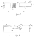
- FIG. 2 shows a cross-sectional view of an optoelectronic component arrangement in which a LED 1 is mounted on a varistor body 2 as a semiconductor device.
- the component arrangement comprises a housing 7, one part of which is shown.
- the varistor body 2 is mounted on the housing 7 and is supported by the latter.
- the varistor body 2 is via a layer, preferably containing aluminum, executed ground terminal 3b contacted with an electrically conductive part of the housing 7.
- the varistor body 2 is contacted to the LED 1 by means of an anode contact 3a designed as a layer or via a first electrical connection.
- the LED is provided on the upper side with a cathode contact 8 designed as a layer or bonding pad.
- the cathode contact 8 has a contact wire connected to the bonding pad, which produces an electrical connection to the corresponding cathode contact 9 of the housing 7.
- the cathode contact 9 of the housing may be designed as a conductor track.
- the housing also has an anode contact 10 designed, for example, as a conductor track, which is brought into electrically conductive connection with the anode contact 3a between the varistor body 2 and the LED 1 by means of a contact wire.
- the first electrical terminal 3a has an area left free by the semiconductor device, which provides space to contact the outside of the same on the same top side of the varistor body.
- the varistor body 2 is provided on its underside with a ground terminal 3b, which contacts a ground contact 13 of the housing 7 which is insulated from the anode part 9 or cathode part 10 of the housing.
- the insulation takes place via an insulating layer 14, which may be designed as part of the housing.
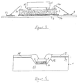
- FIG. 5a shows a plan view of a component arrangement in which on the upper side of the varistor body 2, two separate electrical terminals 3a and 3b are arranged or applied in each case as an electrically conductive layer.
- the first electrical connection 3a which is shown as a dashed frame, contacts a semiconductor component 1 mounted on the varistor body 2, this semiconductor component itself having an electrical connection opposite the electrical connection 3a, for example on its upper side (see, for example, FIGS FIG. 6 ).
- a second electrical connection 3b is likewise arranged on the upper side of the varistor body 2, which contacts the varistor body 2 to the outside, for example to an electrically conductive part 9 of the housing.
- the second electrical connection 3b preferably has, in addition to the metallic layer applied to the varistor body, a contact wire which electrically contacts the varistor with the housing 7.
- FIG. 5b shows a cross-sectional view of the component arrangement according to FIG. 5a , in particular additionally the ground connection 3b on the underside of the component arrangement.
- the varistor body 2 has a varistor-ceramic layer stack, the inner electrode being arranged between two adjacent layers of the stack.
- the varistor body 2 has a plurality of heat-conducting channels 6, which can also be referred to as thermal vias. They run side by side perpendicular to the support surface of the semiconductor device 1 on the varistor body 2 and extend from there to the bottom of the varistor body or up to its base.
- the thermal vias can be designed as vertical holes filled with a good heat conducting material of the varistor body.
- the thermal vias 6 may each comprise metals. According to one embodiment, however, they have a good heat-conducting ceramic, in particular a ceramic, which has a higher thermal conductivity than that of the surrounding material. You can also have a mixture of a metal and a good heat conducting ceramic.
- a single thermal via 6 could also extend from the top to the bottom of the varistor body 2.
- Thermal vias as shown with this figure may be present in the varistor body in all embodiments of the device arrangement described in this document.
- FIG. 8 FIG. 2 also shows that, in addition to the thermal vias 6 (relative to the contact surface of the semiconductor component), a plurality of inner electrodes 4 arranged one above the other are present in the varistor body, which are each connected to a plated-through hole 5.
- a first inner electrode 4 is electrically connected by means of a via 5 to the ground terminal 3b on the underside of the varistor body 2 and contacted the second inner electrode by means of another via 5 with a varistor body outwardly contacting electrical terminal 3b, for example, on the top of the varistor body can be arranged.
- FIG. 9 shows a lying on its longitudinal side Dahl Anlagenvaristorianu 2, wherein between adjacent varistor ceramic layers metal structures are present.
- Below the semiconductor component 1 mounted on the upper longitudinal side of the multilayer varistor body run thin metallic layers which dissipate the heat from the semiconductor component to the housing 7.
- second Electrical connections 3b of the multilayer Varistor stressess 2 wherein one of these terminals is a ground terminal, internal electrodes 4 are connected, wherein in each case a first set of internal electrodes to the ground terminal and a second set of internal electrodes to the further electrical terminal 3b are contacted.
- an inner electrode 4 of the first set is adjacent to an inner electrode 4 of the second set.
Landscapes
- Engineering & Computer Science (AREA)
- Microelectronics & Electronic Packaging (AREA)
- Physics & Mathematics (AREA)
- Electromagnetism (AREA)
- Thermistors And Varistors (AREA)
- Cooling Or The Like Of Electrical Apparatus (AREA)
Applications Claiming Priority (2)
| Application Number | Priority Date | Filing Date | Title |
|---|---|---|---|
| DE102008024479A DE102008024479A1 (de) | 2008-05-21 | 2008-05-21 | Elektrische Bauelementanordnung |
| PCT/EP2009/056247 WO2009141437A1 (de) | 2008-05-21 | 2009-05-22 | Elektrische bauelementanordnung |
Publications (2)
| Publication Number | Publication Date |
|---|---|
| EP2289076A1 EP2289076A1 (de) | 2011-03-02 |
| EP2289076B1 true EP2289076B1 (de) | 2016-04-06 |
Family
ID=41010059
Family Applications (1)
| Application Number | Title | Priority Date | Filing Date |
|---|---|---|---|
| EP09749927.1A Not-in-force EP2289076B1 (de) | 2008-05-21 | 2009-05-22 | Elektrische bauelementanordnung |
Country Status (8)
| Country | Link |
|---|---|
| US (1) | US9177703B2 (https=) |
| EP (1) | EP2289076B1 (https=) |
| JP (1) | JP2011523778A (https=) |
| KR (1) | KR101666230B1 (https=) |
| CN (1) | CN102160129A (https=) |
| DE (1) | DE102008024479A1 (https=) |
| TW (1) | TWI427761B (https=) |
| WO (1) | WO2009141437A1 (https=) |
Families Citing this family (14)
| Publication number | Priority date | Publication date | Assignee | Title |
|---|---|---|---|---|
| DE102008024479A1 (de) * | 2008-05-21 | 2009-12-03 | Epcos Ag | Elektrische Bauelementanordnung |
| WO2012035484A1 (en) * | 2010-09-15 | 2012-03-22 | Koninklijke Philips Electronics N.V. | Embedded transient voltage suppression for light emitting devices |
| TW201221501A (en) * | 2010-11-26 | 2012-06-01 | Sfi Electronics Technology Inc | Process for producing ZnO varistor particularly having internal electrode composed of pure silver and sintered at a lower sintering temperature |
| AU2011334962B2 (en) * | 2010-12-02 | 2015-10-29 | Société des Produits Nestlé S.A. | Low-inertia thermal sensor in a beverage machine |
| DE102012111458B4 (de) * | 2012-11-27 | 2022-12-08 | Tdk Electronics Ag | Halbleitervorrichtung |
| DE102012113014A1 (de) * | 2012-12-21 | 2014-06-26 | Epcos Ag | Bauelementträger und Bauelementträgeranordnung |
| DE102014101092B4 (de) * | 2014-01-29 | 2024-09-12 | Tdk Electronics Ag | Chip mit Schutzfunktion und Verfahren zur Herstellung |
| DE102014020163B4 (de) * | 2014-01-29 | 2025-09-18 | Tdk Electronics Ag | Chip mit Schutzfunktion und Verfahren zur Herstellung |
| DE112014006583B4 (de) * | 2014-05-23 | 2021-05-27 | Mitsubishi Electric Corporation | Überspannungsschutzelement |
| DE102014115375A1 (de) | 2014-08-08 | 2016-02-11 | Epcos Ag | Träger für eine LED |
| DE102016107495B4 (de) * | 2016-04-22 | 2022-04-14 | Tdk Electronics Ag | Vielschicht-Trägersystem, Verfahren zur Herstellung eines Vielschicht-Trägersystems und Verwendung eines Vielschicht-Trägersystems |
| CN106124994A (zh) * | 2016-06-12 | 2016-11-16 | 北京长城华冠汽车科技股份有限公司 | 一种电动汽车的电池参数检测装置和电动汽车 |
| DE102016122014A1 (de) * | 2016-11-16 | 2018-05-17 | Epcos Ag | Leistungsmodul mit verringerter Defektanfälligkeit und Verwendung desselben |
| US10741313B1 (en) | 2019-02-06 | 2020-08-11 | Eaton Intelligent Power Limited | Bus bar assembly with integrated surge arrestor |
Family Cites Families (35)
| Publication number | Priority date | Publication date | Assignee | Title |
|---|---|---|---|---|
| FR2024999A1 (https=) * | 1968-12-02 | 1970-09-04 | Matsushita Electric Industrial Co Ltd | |
| US3928242A (en) * | 1973-11-19 | 1975-12-23 | Gen Electric | Metal oxide varistor with discrete bodies of metallic material therein and method for the manufacture thereof |
| US4272411A (en) * | 1979-03-08 | 1981-06-09 | Electric Power Research Institute | Metal oxide varistor and method |
| JPS6329804B2 (https=) | 1980-09-18 | 1988-06-15 | Tokyo Shibaura Electric Co | |
| JPS58171478A (ja) | 1982-04-02 | 1983-10-08 | Mitsubishi Chem Ind Ltd | 石炭液化方法 |
| US4681717A (en) * | 1986-02-19 | 1987-07-21 | The United States Of America As Represented By The United States Department Of Energy | Process for the chemical preparation of high-field ZnO varistors |
| JPS6325902A (ja) | 1986-07-17 | 1988-02-03 | 株式会社村田製作所 | 電圧非直線抵抗体用磁器組成物 |
| JPS63296307A (ja) | 1987-05-28 | 1988-12-02 | Matsushita Electric Ind Co Ltd | 酸化亜鉛形バリスタの製造方法 |
| JPH07105588B2 (ja) | 1988-02-05 | 1995-11-13 | 富士通株式会社 | 加熱チップの位置決め方式 |
| EP0353166A3 (en) * | 1988-07-25 | 1991-04-10 | John Fluke Mfg. Co., Inc. | Overvoltage protection circuit |
| DE69013252T2 (de) * | 1989-07-11 | 1995-04-27 | Ngk Insulators Ltd | Verfahren zur Herstellung eines nichtlinearen spannungsabhängigen Widerstandes unter Verwendung eines Zinkoxidmaterials. |
| JPH0514104A (ja) | 1991-06-27 | 1993-01-22 | Murata Mfg Co Ltd | ノイズフイルタ |
| US5712757A (en) * | 1996-06-27 | 1998-01-27 | Raychem Corporation | Surge arrester having ridged terminals |
| JPH1197215A (ja) | 1997-09-19 | 1999-04-09 | Fujitsu Ltd | バリスタおよびバリスタ内蔵電源装置 |
| JP2001167908A (ja) * | 1999-12-03 | 2001-06-22 | Tdk Corp | 半導体電子部品 |
| JP3822768B2 (ja) * | 1999-12-03 | 2006-09-20 | 株式会社ルネサステクノロジ | Icカードの製造方法 |
| JP2002110405A (ja) * | 2000-09-28 | 2002-04-12 | Kaho Kagi Kofun Yugenkoshi | 過電圧保護素子の材料及び製造方法 |
| JP2002329872A (ja) * | 2001-04-25 | 2002-11-15 | Kaho Kagi Kofun Yugenkoshi | 過渡過電圧保護素子の材料 |
| US7132922B2 (en) * | 2002-04-08 | 2006-11-07 | Littelfuse, Inc. | Direct application voltage variable material, components thereof and devices employing same |
| JP4292901B2 (ja) * | 2002-08-20 | 2009-07-08 | 株式会社村田製作所 | バリスタ |
| US7279724B2 (en) * | 2004-02-25 | 2007-10-09 | Philips Lumileds Lighting Company, Llc | Ceramic substrate for a light emitting diode where the substrate incorporates ESD protection |
| US20070200133A1 (en) * | 2005-04-01 | 2007-08-30 | Akira Hashimoto | Led assembly and manufacturing method |
| JP2007088173A (ja) | 2005-09-21 | 2007-04-05 | Tdk Corp | 積層型チップバリスタ及び電子機器の製造方法 |
| JP4134135B2 (ja) * | 2005-09-30 | 2008-08-13 | Tdk株式会社 | 発光装置 |
| US7671468B2 (en) * | 2005-09-30 | 2010-03-02 | Tdk Corporation | Light emitting apparatus |
| JP4600309B2 (ja) | 2006-02-13 | 2010-12-15 | Tdk株式会社 | バリスタ及び発光装置 |
| US7696856B2 (en) * | 2006-03-20 | 2010-04-13 | Tdk Corporation | Varistor element |
| JP4984930B2 (ja) * | 2006-03-20 | 2012-07-25 | Tdk株式会社 | バリスタ素子 |
| JP4487963B2 (ja) | 2006-03-27 | 2010-06-23 | Tdk株式会社 | バリスタ及び発光装置 |
| TW200903530A (en) * | 2007-03-30 | 2009-01-16 | Tdk Corp | Voltage non-linear resistance ceramic composition and voltage non-linear resistance element |
| WO2009015298A2 (en) * | 2007-07-25 | 2009-01-29 | Intermolecular, Inc. | Nonvolatile memory elements |
| US8350252B2 (en) * | 2008-03-14 | 2013-01-08 | University Of Connecticut | Boundary-modulated nanoparticle junctions and a method for manufacture thereof |
| US8203421B2 (en) * | 2008-04-14 | 2012-06-19 | Shocking Technologies, Inc. | Substrate device or package using embedded layer of voltage switchable dielectric material in a vertical switching configuration |
| DE102008024479A1 (de) * | 2008-05-21 | 2009-12-03 | Epcos Ag | Elektrische Bauelementanordnung |
| DE102012104494A1 (de) * | 2012-05-24 | 2013-11-28 | Epcos Ag | Leuchtdiodenvorrichtung |
-
2008
- 2008-05-21 DE DE102008024479A patent/DE102008024479A1/de not_active Ceased
-
2009
- 2009-05-20 TW TW098116655A patent/TWI427761B/zh not_active IP Right Cessation
- 2009-05-22 JP JP2011509997A patent/JP2011523778A/ja active Pending
- 2009-05-22 WO PCT/EP2009/056247 patent/WO2009141437A1/de not_active Ceased
- 2009-05-22 EP EP09749927.1A patent/EP2289076B1/de not_active Not-in-force
- 2009-05-22 KR KR1020107028773A patent/KR101666230B1/ko not_active Expired - Fee Related
- 2009-05-22 CN CN200980128602.2A patent/CN102160129A/zh active Pending
- 2009-05-22 US US12/994,146 patent/US9177703B2/en active Active
Also Published As
| Publication number | Publication date |
|---|---|
| CN102160129A (zh) | 2011-08-17 |
| TWI427761B (zh) | 2014-02-21 |
| EP2289076A1 (de) | 2011-03-02 |
| DE102008024479A1 (de) | 2009-12-03 |
| JP2011523778A (ja) | 2011-08-18 |
| US20110188161A1 (en) | 2011-08-04 |
| US9177703B2 (en) | 2015-11-03 |
| KR101666230B1 (ko) | 2016-10-13 |
| KR20110031163A (ko) | 2011-03-24 |
| WO2009141437A1 (de) | 2009-11-26 |
| TW201001668A (en) | 2010-01-01 |
Similar Documents
| Publication | Publication Date | Title |
|---|---|---|
| EP2289076B1 (de) | Elektrische bauelementanordnung | |
| EP2289075B1 (de) | Elektrische bauelementanordnung mit varisor und halbleiterbauelement | |
| EP2289074B1 (de) | Elektrische bauelementanordnung mit einem varistor und einem halbleiterbauelement | |
| EP2856504B1 (de) | Leuchtdiodenvorrichtung | |
| DE10351934B4 (de) | Leuchtdioden-Anordnung mit wärmeabführender Platine | |
| EP2891193B1 (de) | Leuchtdiodenvorrichtung | |
| DE102016107495B4 (de) | Vielschicht-Trägersystem, Verfahren zur Herstellung eines Vielschicht-Trägersystems und Verwendung eines Vielschicht-Trägersystems | |
| WO2004032249A2 (de) | Optoelektronisches bauelement und bauelement-modul | |
| DE102012101606B4 (de) | ESD-Schutzbauelement und Bauelement mit einem ESD-Schutzbauelement und einer LED | |
| DE102012107668A1 (de) | Bauelementanordnung | |
| DE102012101560B4 (de) | Leuchtdiodenvorrichtung | |
| WO2014000988A1 (de) | Optoelektronisches bauelement und verfahren zur herstellung eines optoelektronischen bauelements | |
| DE102007006157A1 (de) | Varistor und Leuchtvorrichtung | |
| EP3178117B1 (de) | Träger für eine led | |
| DE102008054235A1 (de) | Optoelektronisches Bauteil | |
| WO2019081658A1 (de) | Optoelektronischer halbleiterchip | |
| EP2438613A1 (de) | Optoelektronisches halbleiterbauelement |
Legal Events
| Date | Code | Title | Description |
|---|---|---|---|
| PUAI | Public reference made under article 153(3) epc to a published international application that has entered the european phase |
Free format text: ORIGINAL CODE: 0009012 |
|
| 17P | Request for examination filed |
Effective date: 20101217 |
|
| AK | Designated contracting states |
Kind code of ref document: A1 Designated state(s): AT BE BG CH CY CZ DE DK EE ES FI FR GB GR HR HU IE IS IT LI LT LU LV MC MK MT NL NO PL PT RO SE SI SK TR |
|
| AX | Request for extension of the european patent |
Extension state: AL BA RS |
|
| DAX | Request for extension of the european patent (deleted) | ||
| GRAP | Despatch of communication of intention to grant a patent |
Free format text: ORIGINAL CODE: EPIDOSNIGR1 |
|
| INTG | Intention to grant announced |
Effective date: 20151023 |
|
| GRAS | Grant fee paid |
Free format text: ORIGINAL CODE: EPIDOSNIGR3 |
|
| GRAA | (expected) grant |
Free format text: ORIGINAL CODE: 0009210 |
|
| AK | Designated contracting states |
Kind code of ref document: B1 Designated state(s): AT BE BG CH CY CZ DE DK EE ES FI FR GB GR HR HU IE IS IT LI LT LU LV MC MK MT NL NO PL PT RO SE SI SK TR |
|
| REG | Reference to a national code |
Ref country code: GB Ref legal event code: FG4D Free format text: NOT ENGLISH |
|
| REG | Reference to a national code |
Ref country code: AT Ref legal event code: REF Ref document number: 788563 Country of ref document: AT Kind code of ref document: T Effective date: 20160415 Ref country code: CH Ref legal event code: EP |
|
| REG | Reference to a national code |
Ref country code: IE Ref legal event code: FG4D Free format text: LANGUAGE OF EP DOCUMENT: GERMAN |
|
| REG | Reference to a national code |
Ref country code: DE Ref legal event code: R096 Ref document number: 502009012383 Country of ref document: DE |
|
| REG | Reference to a national code |
Ref country code: LT Ref legal event code: MG4D Ref country code: NL Ref legal event code: MP Effective date: 20160406 |
|
| PG25 | Lapsed in a contracting state [announced via postgrant information from national office to epo] |
Ref country code: BE Free format text: LAPSE BECAUSE OF NON-PAYMENT OF DUE FEES Effective date: 20160531 |
|
| PG25 | Lapsed in a contracting state [announced via postgrant information from national office to epo] |
Ref country code: NL Free format text: LAPSE BECAUSE OF FAILURE TO SUBMIT A TRANSLATION OF THE DESCRIPTION OR TO PAY THE FEE WITHIN THE PRESCRIBED TIME-LIMIT Effective date: 20160406 |
|
| PG25 | Lapsed in a contracting state [announced via postgrant information from national office to epo] |
Ref country code: NO Free format text: LAPSE BECAUSE OF FAILURE TO SUBMIT A TRANSLATION OF THE DESCRIPTION OR TO PAY THE FEE WITHIN THE PRESCRIBED TIME-LIMIT Effective date: 20160706 Ref country code: LT Free format text: LAPSE BECAUSE OF FAILURE TO SUBMIT A TRANSLATION OF THE DESCRIPTION OR TO PAY THE FEE WITHIN THE PRESCRIBED TIME-LIMIT Effective date: 20160406 Ref country code: IS Free format text: LAPSE BECAUSE OF FAILURE TO SUBMIT A TRANSLATION OF THE DESCRIPTION OR TO PAY THE FEE WITHIN THE PRESCRIBED TIME-LIMIT Effective date: 20160806 Ref country code: PL Free format text: LAPSE BECAUSE OF FAILURE TO SUBMIT A TRANSLATION OF THE DESCRIPTION OR TO PAY THE FEE WITHIN THE PRESCRIBED TIME-LIMIT Effective date: 20160406 Ref country code: FI Free format text: LAPSE BECAUSE OF FAILURE TO SUBMIT A TRANSLATION OF THE DESCRIPTION OR TO PAY THE FEE WITHIN THE PRESCRIBED TIME-LIMIT Effective date: 20160406 |
|
| PG25 | Lapsed in a contracting state [announced via postgrant information from national office to epo] |
Ref country code: HR Free format text: LAPSE BECAUSE OF FAILURE TO SUBMIT A TRANSLATION OF THE DESCRIPTION OR TO PAY THE FEE WITHIN THE PRESCRIBED TIME-LIMIT Effective date: 20160406 Ref country code: GR Free format text: LAPSE BECAUSE OF FAILURE TO SUBMIT A TRANSLATION OF THE DESCRIPTION OR TO PAY THE FEE WITHIN THE PRESCRIBED TIME-LIMIT Effective date: 20160707 Ref country code: SE Free format text: LAPSE BECAUSE OF FAILURE TO SUBMIT A TRANSLATION OF THE DESCRIPTION OR TO PAY THE FEE WITHIN THE PRESCRIBED TIME-LIMIT Effective date: 20160406 Ref country code: PT Free format text: LAPSE BECAUSE OF FAILURE TO SUBMIT A TRANSLATION OF THE DESCRIPTION OR TO PAY THE FEE WITHIN THE PRESCRIBED TIME-LIMIT Effective date: 20160808 Ref country code: ES Free format text: LAPSE BECAUSE OF FAILURE TO SUBMIT A TRANSLATION OF THE DESCRIPTION OR TO PAY THE FEE WITHIN THE PRESCRIBED TIME-LIMIT Effective date: 20160406 Ref country code: LV Free format text: LAPSE BECAUSE OF FAILURE TO SUBMIT A TRANSLATION OF THE DESCRIPTION OR TO PAY THE FEE WITHIN THE PRESCRIBED TIME-LIMIT Effective date: 20160406 |
|
| PG25 | Lapsed in a contracting state [announced via postgrant information from national office to epo] |
Ref country code: IT Free format text: LAPSE BECAUSE OF FAILURE TO SUBMIT A TRANSLATION OF THE DESCRIPTION OR TO PAY THE FEE WITHIN THE PRESCRIBED TIME-LIMIT Effective date: 20160406 |
|
| REG | Reference to a national code |
Ref country code: CH Ref legal event code: PL |
|
| REG | Reference to a national code |
Ref country code: DE Ref legal event code: R097 Ref document number: 502009012383 Country of ref document: DE |
|
| PG25 | Lapsed in a contracting state [announced via postgrant information from national office to epo] |
Ref country code: CH Free format text: LAPSE BECAUSE OF NON-PAYMENT OF DUE FEES Effective date: 20160531 Ref country code: RO Free format text: LAPSE BECAUSE OF FAILURE TO SUBMIT A TRANSLATION OF THE DESCRIPTION OR TO PAY THE FEE WITHIN THE PRESCRIBED TIME-LIMIT Effective date: 20160406 Ref country code: MC Free format text: LAPSE BECAUSE OF FAILURE TO SUBMIT A TRANSLATION OF THE DESCRIPTION OR TO PAY THE FEE WITHIN THE PRESCRIBED TIME-LIMIT Effective date: 20160406 Ref country code: SK Free format text: LAPSE BECAUSE OF FAILURE TO SUBMIT A TRANSLATION OF THE DESCRIPTION OR TO PAY THE FEE WITHIN THE PRESCRIBED TIME-LIMIT Effective date: 20160406 Ref country code: CZ Free format text: LAPSE BECAUSE OF FAILURE TO SUBMIT A TRANSLATION OF THE DESCRIPTION OR TO PAY THE FEE WITHIN THE PRESCRIBED TIME-LIMIT Effective date: 20160406 Ref country code: EE Free format text: LAPSE BECAUSE OF FAILURE TO SUBMIT A TRANSLATION OF THE DESCRIPTION OR TO PAY THE FEE WITHIN THE PRESCRIBED TIME-LIMIT Effective date: 20160406 Ref country code: LI Free format text: LAPSE BECAUSE OF NON-PAYMENT OF DUE FEES Effective date: 20160531 Ref country code: DK Free format text: LAPSE BECAUSE OF FAILURE TO SUBMIT A TRANSLATION OF THE DESCRIPTION OR TO PAY THE FEE WITHIN THE PRESCRIBED TIME-LIMIT Effective date: 20160406 |
|
| PLBE | No opposition filed within time limit |
Free format text: ORIGINAL CODE: 0009261 |
|
| STAA | Information on the status of an ep patent application or granted ep patent |
Free format text: STATUS: NO OPPOSITION FILED WITHIN TIME LIMIT |
|
| REG | Reference to a national code |
Ref country code: IE Ref legal event code: MM4A |
|
| REG | Reference to a national code |
Ref country code: FR Ref legal event code: ST Effective date: 20170131 |
|
| 26N | No opposition filed |
Effective date: 20170110 |
|
| GBPC | Gb: european patent ceased through non-payment of renewal fee |
Effective date: 20160706 |
|
| PG25 | Lapsed in a contracting state [announced via postgrant information from national office to epo] |
Ref country code: FR Free format text: LAPSE BECAUSE OF NON-PAYMENT OF DUE FEES Effective date: 20160606 |
|
| PG25 | Lapsed in a contracting state [announced via postgrant information from national office to epo] |
Ref country code: GB Free format text: LAPSE BECAUSE OF NON-PAYMENT OF DUE FEES Effective date: 20160706 Ref country code: IE Free format text: LAPSE BECAUSE OF NON-PAYMENT OF DUE FEES Effective date: 20160522 Ref country code: SI Free format text: LAPSE BECAUSE OF FAILURE TO SUBMIT A TRANSLATION OF THE DESCRIPTION OR TO PAY THE FEE WITHIN THE PRESCRIBED TIME-LIMIT Effective date: 20160406 |
|
| REG | Reference to a national code |
Ref country code: AT Ref legal event code: MM01 Ref document number: 788563 Country of ref document: AT Kind code of ref document: T Effective date: 20160522 |
|
| PG25 | Lapsed in a contracting state [announced via postgrant information from national office to epo] |
Ref country code: AT Free format text: LAPSE BECAUSE OF NON-PAYMENT OF DUE FEES Effective date: 20160522 |
|
| PG25 | Lapsed in a contracting state [announced via postgrant information from national office to epo] |
Ref country code: CY Free format text: LAPSE BECAUSE OF FAILURE TO SUBMIT A TRANSLATION OF THE DESCRIPTION OR TO PAY THE FEE WITHIN THE PRESCRIBED TIME-LIMIT Effective date: 20160406 Ref country code: HU Free format text: LAPSE BECAUSE OF FAILURE TO SUBMIT A TRANSLATION OF THE DESCRIPTION OR TO PAY THE FEE WITHIN THE PRESCRIBED TIME-LIMIT; INVALID AB INITIO Effective date: 20090522 |
|
| PG25 | Lapsed in a contracting state [announced via postgrant information from national office to epo] |
Ref country code: TR Free format text: LAPSE BECAUSE OF FAILURE TO SUBMIT A TRANSLATION OF THE DESCRIPTION OR TO PAY THE FEE WITHIN THE PRESCRIBED TIME-LIMIT Effective date: 20160406 Ref country code: MT Free format text: LAPSE BECAUSE OF FAILURE TO SUBMIT A TRANSLATION OF THE DESCRIPTION OR TO PAY THE FEE WITHIN THE PRESCRIBED TIME-LIMIT Effective date: 20160406 Ref country code: LU Free format text: LAPSE BECAUSE OF NON-PAYMENT OF DUE FEES Effective date: 20160522 Ref country code: MK Free format text: LAPSE BECAUSE OF FAILURE TO SUBMIT A TRANSLATION OF THE DESCRIPTION OR TO PAY THE FEE WITHIN THE PRESCRIBED TIME-LIMIT Effective date: 20160406 |
|
| PG25 | Lapsed in a contracting state [announced via postgrant information from national office to epo] |
Ref country code: BG Free format text: LAPSE BECAUSE OF FAILURE TO SUBMIT A TRANSLATION OF THE DESCRIPTION OR TO PAY THE FEE WITHIN THE PRESCRIBED TIME-LIMIT Effective date: 20160406 |
|
| REG | Reference to a national code |
Ref country code: DE Ref legal event code: R082 Ref document number: 502009012383 Country of ref document: DE Representative=s name: EPPING HERMANN FISCHER PATENTANWALTSGESELLSCHA, DE Ref country code: DE Ref legal event code: R081 Ref document number: 502009012383 Country of ref document: DE Owner name: TDK ELECTRONICS AG, DE Free format text: FORMER OWNER: EPCOS AG, 81669 MUENCHEN, DE |
|
| P01 | Opt-out of the competence of the unified patent court (upc) registered |
Effective date: 20230521 |
|
| PGFP | Annual fee paid to national office [announced via postgrant information from national office to epo] |
Ref country code: DE Payment date: 20230523 Year of fee payment: 15 |
|
| REG | Reference to a national code |
Ref country code: DE Ref legal event code: R119 Ref document number: 502009012383 Country of ref document: DE |
|
| PG25 | Lapsed in a contracting state [announced via postgrant information from national office to epo] |
Ref country code: DE Free format text: LAPSE BECAUSE OF NON-PAYMENT OF DUE FEES Effective date: 20241203 |