EP2289076B1 - Electric component assembly - Google Patents
Electric component assembly Download PDFInfo
- Publication number
- EP2289076B1 EP2289076B1 EP09749927.1A EP09749927A EP2289076B1 EP 2289076 B1 EP2289076 B1 EP 2289076B1 EP 09749927 A EP09749927 A EP 09749927A EP 2289076 B1 EP2289076 B1 EP 2289076B1
- Authority
- EP
- European Patent Office
- Prior art keywords
- varistor body
- varistor
- arrangement according
- component
- component arrangement
- Prior art date
- Legal status (The legal status is an assumption and is not a legal conclusion. Google has not performed a legal analysis and makes no representation as to the accuracy of the status listed.)
- Active
Links
Images


Classifications
-
- H—ELECTRICITY
- H01—ELECTRIC ELEMENTS
- H01C—RESISTORS
- H01C7/00—Non-adjustable resistors formed as one or more layers or coatings; Non-adjustable resistors made from powdered conducting material or powdered semi-conducting material with or without insulating material
- H01C7/10—Non-adjustable resistors formed as one or more layers or coatings; Non-adjustable resistors made from powdered conducting material or powdered semi-conducting material with or without insulating material voltage responsive, i.e. varistors
- H01C7/12—Overvoltage protection resistors
-
- H—ELECTRICITY
- H01—ELECTRIC ELEMENTS
- H01C—RESISTORS
- H01C7/00—Non-adjustable resistors formed as one or more layers or coatings; Non-adjustable resistors made from powdered conducting material or powdered semi-conducting material with or without insulating material
- H01C7/10—Non-adjustable resistors formed as one or more layers or coatings; Non-adjustable resistors made from powdered conducting material or powdered semi-conducting material with or without insulating material voltage responsive, i.e. varistors
- H01C7/102—Varistor boundary, e.g. surface layers
-
- H—ELECTRICITY
- H01—ELECTRIC ELEMENTS
- H01C—RESISTORS
- H01C7/00—Non-adjustable resistors formed as one or more layers or coatings; Non-adjustable resistors made from powdered conducting material or powdered semi-conducting material with or without insulating material
- H01C7/10—Non-adjustable resistors formed as one or more layers or coatings; Non-adjustable resistors made from powdered conducting material or powdered semi-conducting material with or without insulating material voltage responsive, i.e. varistors
- H01C7/105—Varistor cores
-
- H—ELECTRICITY
- H01—ELECTRIC ELEMENTS
- H01L—SEMICONDUCTOR DEVICES NOT COVERED BY CLASS H10
- H01L2224/00—Indexing scheme for arrangements for connecting or disconnecting semiconductor or solid-state bodies and methods related thereto as covered by H01L24/00
- H01L2224/01—Means for bonding being attached to, or being formed on, the surface to be connected, e.g. chip-to-package, die-attach, "first-level" interconnects; Manufacturing methods related thereto
- H01L2224/42—Wire connectors; Manufacturing methods related thereto
- H01L2224/47—Structure, shape, material or disposition of the wire connectors after the connecting process
- H01L2224/48—Structure, shape, material or disposition of the wire connectors after the connecting process of an individual wire connector
- H01L2224/4805—Shape
- H01L2224/4809—Loop shape
- H01L2224/48091—Arched
-
- H—ELECTRICITY
- H01—ELECTRIC ELEMENTS
- H01L—SEMICONDUCTOR DEVICES NOT COVERED BY CLASS H10
- H01L2224/00—Indexing scheme for arrangements for connecting or disconnecting semiconductor or solid-state bodies and methods related thereto as covered by H01L24/00
- H01L2224/01—Means for bonding being attached to, or being formed on, the surface to be connected, e.g. chip-to-package, die-attach, "first-level" interconnects; Manufacturing methods related thereto
- H01L2224/42—Wire connectors; Manufacturing methods related thereto
- H01L2224/47—Structure, shape, material or disposition of the wire connectors after the connecting process
- H01L2224/48—Structure, shape, material or disposition of the wire connectors after the connecting process of an individual wire connector
- H01L2224/484—Connecting portions
- H01L2224/48463—Connecting portions the connecting portion on the bonding area of the semiconductor or solid-state body being a ball bond
- H01L2224/48465—Connecting portions the connecting portion on the bonding area of the semiconductor or solid-state body being a ball bond the other connecting portion not on the bonding area being a wedge bond, i.e. ball-to-wedge, regular stitch
-
- H—ELECTRICITY
- H01—ELECTRIC ELEMENTS
- H01L—SEMICONDUCTOR DEVICES NOT COVERED BY CLASS H10
- H01L2224/00—Indexing scheme for arrangements for connecting or disconnecting semiconductor or solid-state bodies and methods related thereto as covered by H01L24/00
- H01L2224/01—Means for bonding being attached to, or being formed on, the surface to be connected, e.g. chip-to-package, die-attach, "first-level" interconnects; Manufacturing methods related thereto
- H01L2224/42—Wire connectors; Manufacturing methods related thereto
- H01L2224/47—Structure, shape, material or disposition of the wire connectors after the connecting process
- H01L2224/48—Structure, shape, material or disposition of the wire connectors after the connecting process of an individual wire connector
- H01L2224/484—Connecting portions
- H01L2224/48475—Connecting portions connected to auxiliary connecting means on the bonding areas, e.g. pre-ball, wedge-on-ball, ball-on-ball
- H01L2224/48476—Connecting portions connected to auxiliary connecting means on the bonding areas, e.g. pre-ball, wedge-on-ball, ball-on-ball between the wire connector and the bonding area
- H01L2224/48477—Connecting portions connected to auxiliary connecting means on the bonding areas, e.g. pre-ball, wedge-on-ball, ball-on-ball between the wire connector and the bonding area being a pre-ball (i.e. a ball formed by capillary bonding)
- H01L2224/48478—Connecting portions connected to auxiliary connecting means on the bonding areas, e.g. pre-ball, wedge-on-ball, ball-on-ball between the wire connector and the bonding area being a pre-ball (i.e. a ball formed by capillary bonding) the connecting portion being a wedge bond, i.e. wedge on pre-ball
- H01L2224/4848—Connecting portions connected to auxiliary connecting means on the bonding areas, e.g. pre-ball, wedge-on-ball, ball-on-ball between the wire connector and the bonding area being a pre-ball (i.e. a ball formed by capillary bonding) the connecting portion being a wedge bond, i.e. wedge on pre-ball outside the semiconductor or solid-state body
Definitions
- An object to be solved is to provide a device or means by which or with which an electrical component can be gently protected against overvoltages.
- the invention is defined by the features of claim 1.
- a semiconductor component is mounted on a varistor body or is supported by this.
- the varistor body is electrically contacted with this to protect the electrical component.
- the semiconductor component and the varistor body are preferably interconnected electrically in parallel.
- the varistor body contains a composite material which is composed of at least one varistor ceramic and a good heat-conducting material, wherein the good heat-conducting material differs from the varistor ceramic, which is selected mainly for non-linear resistance function of the varistor body.
- one or more layers of a varistor body designed as a multilayer varistor may comprise zirconium oxide.
- the cover layer of the multilayer varistor on which the semiconductor component is mounted contains zirconium oxide.
- the base layer also contains zirconium oxide in order to achieve the same effect as described above with respect to the housing or printed circuit board.
- the varistor body has a plurality of electrical connections, of which at least one first electrical connection makes contact with the semiconductor component.
- This electrical connection is preferably designed as a metallic layer.
- the metallic layer can be applied to at least one area of the upper side of the varistor body, for example by screen printing.
- the component arrangement is provided with a designed as a layer of electrical connection a particularly compact form.
- other forms of electrical connections are conceivable, such as e.g. a contact wire.
- Both a first electrical connection and a second electrical connection can be embodied as metallic layers.
- Electrical connections of the varistor body designed as metallic layers may contain at least one of the following materials: gold, nickel, chromium, palladium.
- the semiconductor component has a flip-chip contact on its mounting side or underside.
- the Flipchiprome ist may have an array or an array of solder balls on the underside of the semiconductor device.
- the varistor body serves as a thermomechanical buffer between the semiconductor component and the housing.
- An LED as a semiconductor device is preferably composed of one or more of the following materials: gallium phosphide (GaP), gallium nitride (GaN), gallium arsenic phosphide (GaAsP), aluminum gallium indium phosphide (AlGaInP), aluminum gallium phosphide (AlGaP), aluminum gallium arsenide (AlGaAs), indium gallium nitride (InGaN), aluminum nitride (AlN), aluminum gallium indium nitride (AlGaInN), tin selenide (ZnSe).
- GaP gallium phosphide
- GaN gallium nitride
- GaAsP gallium arsenic phosphide
- AlGaInP aluminum gallium indium phosphide
- AlGaP aluminum gallium phosphide
- AlGaAs aluminum gallium arsenide
- FIG. 1b shows how the varistor body 2 according to FIG. 1a is provided on its underside with a designed as a contact layer second electrical connection 3b, which may serve as a cathode or ground contact, for example. It is preferred that the lower contact layer 3b is one containing aluminum, preferably mostly.
- the contact layer 3b is preferably used for contacting the varistor body 2 to the outside, for example for contacting with a housing or with its electrically conductive part.
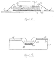
- FIG. 2 shows a cross-sectional view of an optoelectronic component arrangement in which a LED 1 is mounted on a varistor body 2 as a semiconductor device.
- the component arrangement comprises a housing 7, one part of which is shown.
- the varistor body 2 is mounted on the housing 7 and is supported by the latter.
- the varistor body 2 is via a layer, preferably containing aluminum, executed ground terminal 3b contacted with an electrically conductive part of the housing 7.
- the varistor body 2 is contacted to the LED 1 by means of an anode contact 3a designed as a layer or via a first electrical connection.
- the LED is provided on the upper side with a cathode contact 8 designed as a layer or bonding pad.
- the cathode contact 8 has a contact wire connected to the bonding pad, which produces an electrical connection to the corresponding cathode contact 9 of the housing 7.
- the cathode contact 9 of the housing may be designed as a conductor track.
- the housing also has an anode contact 10 designed, for example, as a conductor track, which is brought into electrically conductive connection with the anode contact 3a between the varistor body 2 and the LED 1 by means of a contact wire.
- the first electrical terminal 3a has an area left free by the semiconductor device, which provides space to contact the outside of the same on the same top side of the varistor body.
- the varistor body 2 is provided on its underside with a ground terminal 3b, which contacts a ground contact 13 of the housing 7 which is insulated from the anode part 9 or cathode part 10 of the housing.
- the insulation takes place via an insulating layer 14, which may be designed as part of the housing.
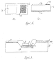
- FIG. 5a shows a plan view of a component arrangement in which on the upper side of the varistor body 2, two separate electrical terminals 3a and 3b are arranged or applied in each case as an electrically conductive layer.
- the first electrical connection 3a which is shown as a dashed frame, contacts a semiconductor component 1 mounted on the varistor body 2, this semiconductor component itself having an electrical connection opposite the electrical connection 3a, for example on its upper side (see, for example, FIGS FIG. 6 ).
- a second electrical connection 3b is likewise arranged on the upper side of the varistor body 2, which contacts the varistor body 2 to the outside, for example to an electrically conductive part 9 of the housing.
- the second electrical connection 3b preferably has, in addition to the metallic layer applied to the varistor body, a contact wire which electrically contacts the varistor with the housing 7.
- FIG. 5b shows a cross-sectional view of the component arrangement according to FIG. 5a , in particular additionally the ground connection 3b on the underside of the component arrangement.
- the varistor body 2 has a varistor-ceramic layer stack, the inner electrode being arranged between two adjacent layers of the stack.
- the varistor body 2 has a plurality of heat-conducting channels 6, which can also be referred to as thermal vias. They run side by side perpendicular to the support surface of the semiconductor device 1 on the varistor body 2 and extend from there to the bottom of the varistor body or up to its base.
- the thermal vias can be designed as vertical holes filled with a good heat conducting material of the varistor body.
- the thermal vias 6 may each comprise metals. According to one embodiment, however, they have a good heat-conducting ceramic, in particular a ceramic, which has a higher thermal conductivity than that of the surrounding material. You can also have a mixture of a metal and a good heat conducting ceramic.
- a single thermal via 6 could also extend from the top to the bottom of the varistor body 2.
- Thermal vias as shown with this figure may be present in the varistor body in all embodiments of the device arrangement described in this document.
- FIG. 8 FIG. 2 also shows that, in addition to the thermal vias 6 (relative to the contact surface of the semiconductor component), a plurality of inner electrodes 4 arranged one above the other are present in the varistor body, which are each connected to a plated-through hole 5.
- a first inner electrode 4 is electrically connected by means of a via 5 to the ground terminal 3b on the underside of the varistor body 2 and contacted the second inner electrode by means of another via 5 with a varistor body outwardly contacting electrical terminal 3b, for example, on the top of the varistor body can be arranged.
- FIG. 9 shows a lying on its longitudinal side Dahl Anlagenvaristorianu 2, wherein between adjacent varistor ceramic layers metal structures are present.
- Below the semiconductor component 1 mounted on the upper longitudinal side of the multilayer varistor body run thin metallic layers which dissipate the heat from the semiconductor component to the housing 7.
- second Electrical connections 3b of the multilayer Varistor stressess 2 wherein one of these terminals is a ground terminal, internal electrodes 4 are connected, wherein in each case a first set of internal electrodes to the ground terminal and a second set of internal electrodes to the further electrical terminal 3b are contacted.
- an inner electrode 4 of the first set is adjacent to an inner electrode 4 of the second set.
Landscapes
- Engineering & Computer Science (AREA)
- Microelectronics & Electronic Packaging (AREA)
- Physics & Mathematics (AREA)
- Electromagnetism (AREA)
- Thermistors And Varistors (AREA)
- Cooling Or The Like Of Electrical Apparatus (AREA)
Description
Es wird eine Anordnung von elektrischen Bauelementen, insbesondere mit Mittel zum Schutz vor Überspannungen, beschrieben.An arrangement of electrical components, in particular with means for protection against overvoltages, is described.
Aus
Aus
Eine zu lösende Aufgabe besteht darin, ein Vorrichtung bzw. Mittel anzugeben, mit der bzw. mit denen ein elektrisches Bauelement schonend vor Überspannungen geschützt werden kann.An object to be solved is to provide a device or means by which or with which an electrical component can be gently protected against overvoltages.
Die Erfindung ist mit den Merkmale des Anspruchs 1 definiert.The invention is defined by the features of
Es wird vorgeschlagen, dass in einer elektrischen Bauelementanordnung ein Halbleiterbauelement auf einem Varistorkörper montiert ist bzw. von diesem getragen wird. Der Varistorkörper ist zum Schutz des elektrischen Bauelements mit diesem elektrisch kontaktiert. Das Halbleiterbauelement und der Varistorkörper sind vorzugsweise elektrisch parallel miteinander verschaltet.It is proposed that in a electrical component arrangement, a semiconductor component is mounted on a varistor body or is supported by this. The varistor body is electrically contacted with this to protect the electrical component. The semiconductor component and the varistor body are preferably interconnected electrically in parallel.
Der Varistorkörper ist als eigenständige mechanische Einheit gebildet und als Träger des Halbleiterbauelements zu verstehen. Er kann vom Halbleiterbauelement separat hergestellt werden und weist eine Form auf, die dem Halbleiterbauelement eine Auflage- bzw. Montagefläche bietet.The varistor body is formed as an independent mechanical unit and to be understood as a carrier of the semiconductor device. It can be manufactured separately from the semiconductor component and has a shape which offers the semiconductor component a support or mounting surface.
Mittels des als Träger für das Halbleiterbauelement dienenden Varistorkörpers wird dem Halbleiterbauelement ein einfaches Mittel zum Schutz gegenüber Überspannungen, insbesondere gegenüber elektrostatischen Entladungen, geboten, wobei das Halbleiterbauelement vorteilhafterweise selbst zu diesem Zweck nicht weitergebildet bzw. angepasst werden muss. Der Varistorkörper kann zum Zweck des bestmöglichen Schutzes vor Überspannungen eines mit dem Varistorkörper gekoppelten Halbleiterbauelements ohne Berücksichtigung der Bauform des Halbleiterbauelements separat hergestellt bzw. entworfen werden. Die Funktion des Schutzes vor Überspannungen des Varistorkörpers darf somit ohne einer durch die Struktur des Halbleiterbauelements bedingten Einschränkung voll ausgeschöpft werden.By means of the varistor body serving as a support for the semiconductor component, the semiconductor component is provided with a simple means of protection against overvoltages, in particular with respect to electrostatic discharges, wherein the Semiconductor device advantageously even for this purpose does not need to be further developed or adapted. The varistor body can be manufactured or designed separately for the purpose of the best possible protection against overvoltages of a semiconductor device coupled to the varistor body without consideration of the design of the semiconductor device. The function of protection against overvoltages of the varistor body may thus be fully utilized without a restriction imposed by the structure of the semiconductor device.
Gemäß einer bevorzugten Ausführungsform der Bauelementanordnung enthält der Varistorkörper ein Kompositmaterial, das zumindest aus einer Varistorkeramik und einem gut wärmeleitenden Material zusammengesetzt ist, wobei das gut wärmeleitende Material sich von der Varistorkeramik, die hauptsächlich zur nichtlinearen Widerstandsfunktion des Varistkörpers gewählt ist, unterscheidet.According to a preferred embodiment of the component arrangement, the varistor body contains a composite material which is composed of at least one varistor ceramic and a good heat-conducting material, wherein the good heat-conducting material differs from the varistor ceramic, which is selected mainly for non-linear resistance function of the varistor body.
Gemäß einer Ausführungsform ist die Varistorkeramik als Hauptkomponente bzw. als Matrix des Kompositmaterials und das wärmeleitende Material als Füllstoff in dieser Matrix gebildet. Ein Beispiel eines gut wärmeleitenden Füllstoffs ist ein Metall; insbesondere sind Metalle mit einer Wärmeleitfähigkeit größer 100 W/(m*K) und Edelmetalle der 2. und 3. Übergangsmetallperiode bzw. deren Legierungen zu nennen. Der Füllstoff liegt vorzugsweise als eine Verteilung von gut wärmeleitenden Partikeln im Varistorkörper vor.According to one embodiment, the varistor ceramic is formed as a main component or as a matrix of the composite material and the heat-conducting material as a filler in this matrix. An example of a good heat-conducting filler is a metal; In particular, metals with a thermal conductivity greater than 100 W / (m * K) and precious metals of the second and third transition metal period or their alloys may be mentioned. The filler is preferably present as a distribution of highly thermally conductive particles in the varistor body.
Ein vorzugsweise als Füllstoff in der Varistorkeramik vorliegendes Metall hat den Vorteil, dem Varistorkörper eine höhere Wärmeleitfähigkeit zu verleihen, so dass auch Wärme vom Halbleiterbauelement über den Varistorkörper abgeleitet werden kann. Somit kann der Varistorkörper gleichzeitig zwei Funktionen aufweisen: die des Schutzes vor Überspannungen und die der Wärmeableitung.A metal preferably present as a filler in the varistor ceramic has the advantage of giving the varistor body a higher thermal conductivity, so that also heat is dissipated from the semiconductor component via the varistor body can be. Thus, the varistor body can simultaneously have two functions: the protection against overvoltages and the heat dissipation.
Vorteilhaft ist eine Ausführungsform, bei der der Varistorkörper eine gut wärmeleitende Keramik enthält, die sich von der Varistorkeramik unterscheidet bzw. eine höhere Wärmeleitfähigkeit aufweist, als die Varistorkeramik. Als geeignete Keramiken haben sich zum Beispiel Aluminiumnitrid, Siliziumkarbid, Hafniumoxid und Manganoxid herausgestellt, insbesondere auch deshalb, weil sie sich mit einer bevorzugten Varistorkeramik wie zum Beispiel Zinkoxid gut versintern lassen, ohne dass sich unerwünschte kristalline Unterbrechungen im Varistorkörper ausbilden. Die zusätzliche, gut wärmeleitende Keramik kann ähnlich wie beim Metall als Füllstoff in der als Matrix ausgeführten Varistorkeramik vorliegen.Advantageous is an embodiment in which the varistor body contains a good heat-conducting ceramic, which differs from the varistor ceramic or has a higher thermal conductivity than the varistor ceramic. Aluminum nitride, silicon carbide, hafnium oxide and manganese oxide, for example, have proven to be suitable ceramics, in particular because they can be sintered well with a preferred varistor ceramic such as zinc oxide, without formation of undesired crystalline interruptions in the varistor body. The additional, highly thermally conductive ceramic may be similar to the metal as a filler in the running as a matrix varistor ceramic.
Der Varistorkörper kann als Vielschichtvaristor mit einem Stapel von Varistorkeramikschichten und zumindest bereichsweise dazwischenliegenden Innenelektrodenschichten ausgeführt sein. Es wird bevorzugt, dass der Vielschichtvaristor ein gesintertes, monolithisches Vielschichtbauelement ist. Als Varistorkeramik der einzelnen Schichten wird hauptanteilig Zinkoxid gewählt, wobei die Innenelektroden Silber, Palladium, Platin, Kupfer, Nickel oder eine Legierung dieser Materialien enthalten können.The varistor body can be embodied as a multilayer varistor with a stack of varistor ceramic layers and inner electrode layers intervening at least in some areas. It is preferred that the multilayer varistor is a sintered monolithic multilayer device. As the varistor ceramic of the individual layers, zinc oxide is selected to a large extent, it being possible for the internal electrodes to contain silver, palladium, platinum, copper, nickel or an alloy of these materials.
Nach einer Ausführungsform können ein oder mehrere Schichten eines als Vielschichtvaristor ausgebildeten Varistorkörpers Zirkonoxid aufweisen. Dabei wird bevorzugt, dass zumindest die Deckschicht des Vielschichtvaristors, auf der das Halbleiterbauelement montiert ist, Zirkonoxid enthält. Dadurch können die Einflüsse von Streukapazitäten des Vielschichtvaristors auf dem Halbleiterbauelement reduziert werden. Ist der Vielschichtvaristor in einem Gehäuse integriert bzw. liegt der Vielschichtvaristor auf einer Leiterplatte, so wird bevorzugt, dass auch die Grundschicht Zirkonoxid enthält um den gleichen oben beschriebenen Effekt gegenüber dem Gehäuse bzw. der Leiterplatte zu erreichen.According to one embodiment, one or more layers of a varistor body designed as a multilayer varistor may comprise zirconium oxide. In this case, it is preferred that at least the cover layer of the multilayer varistor on which the semiconductor component is mounted contains zirconium oxide. As a result, the influences of stray capacitances of the multilayer varistor on the semiconductor component can be reduced. If the multilayer varistor is integrated in a housing or if the multilayer varistor is located on a printed circuit board, it is preferred that the base layer also contains zirconium oxide in order to achieve the same effect as described above with respect to the housing or printed circuit board.
Anstelle eines Vielschichtvaristors kann ein Bulkvaristor als Träger für das Halbleiterbauelement dienen. Dieser weist an seiner Außenseite gegenpolige Außenkontakte auf, ist im Innern jedoch frei von metallischen Schichten.Instead of a multilayer varistor, a bulk varistor can serve as a carrier for the semiconductor component. This has on its outer side opposite polarity external contacts, but is internally free of metallic layers.
Gemäß einer Ausführungsform weist der Varistorkörper mehrere elektrische Anschlüsse auf, von denen zumindest ein erster elektrischer Anschluss das Halbleiterbauelement kontaktiert. Dieser elektrische Anschluss ist vorzugsweise als metallische Schicht ausgeführt. Die metallische Schicht kann auf zumindest einem Bereich der Oberseite des Varistorkörpers aufgebracht sein, beispielsweise mittels Siebdrucken. Der Bauelementanordnung wird mit einem als Schicht ausgeführten elektrischen Anschluss eine besonders kompakte Form geboten. Andere Formen von elektrischen Anschlüssen sind jedoch denkbar, wie z.B. ein Kontaktdraht.According to one embodiment, the varistor body has a plurality of electrical connections, of which at least one first electrical connection makes contact with the semiconductor component. This electrical connection is preferably designed as a metallic layer. The metallic layer can be applied to at least one area of the upper side of the varistor body, for example by screen printing. The component arrangement is provided with a designed as a layer of electrical connection a particularly compact form. However, other forms of electrical connections are conceivable, such as e.g. a contact wire.
Gemäß einer Ausführungsform der Bauelementanordnung umfassen die mehreren elektrischen Anschlüsse des Varistorkörpers zumindest einen vom ersten elektrischen Anschluss separaten, zweiten elektrischen Anschluss, der den Varistorkörper nach außen kontaktiert, welches bedeutet, dass der Varistor mit diesem zweiten elektrischen Anschluss mit einem vom Halbleiterbauelement getrennten zweiten elektrischen Potential verbunden ist. Dabei kann der zweite elektrische Anschluss mit einer Leiterbahn auf einer Leiterplatte kontaktiert sein. Es kann sich bei einem zweiten elektrischen Anschluss beispielsweise um einen Masseanschluss handeln.According to one embodiment of the component arrangement, the plurality of electrical terminals of the varistor body comprise at least one second electrical connection separate from the first electrical connection, which contacts the varistor body to the outside, which means that the varistor with this second electrical connection has a second electrical potential separated from the semiconductor component connected is. In this case, the second electrical Connection to be contacted with a conductor on a circuit board. For example, a second electrical connection may be a ground connection.
Sowohl ein erster elektrischer Anschluss als auch ein zweiter elektrischer Anschluss können als metallische Schichten ausgeführt sein. Als metallische Schichten ausgeführte elektrische Anschlüsse des Varistorkörpers können zumindest eines der folgenden Materialien enthalten: Gold, Nickel, Chromium, Palladium.Both a first electrical connection and a second electrical connection can be embodied as metallic layers. Electrical connections of the varistor body designed as metallic layers may contain at least one of the following materials: gold, nickel, chromium, palladium.
Gemäß einer Ausführungsform der Bauelementanordnung ist der zweite elektrische Anschluss, der den Varistorkörper nach außen kontaktiert, auf der Unterseite des Varistorkörpers, d.h., auf der der Montagefläche des Halbleiterbauelements senkrecht gegenüberliegenden Fläche, angeordnet. Der zweite elektrische Anschluss kann beispielsweise als Bondpad ausgeführt sein. Dieser zweite elektrische Anschluss kann mit einer elektrisch leitenden Struktur einer Leiterplatte oder eines Gehäuses kontaktiert werden. Der zweite elektrische Anschluss kann darüber hinaus einen Kontaktdraht umfassen, wobei dieser beispielsweise mit einem vom elektrischen Anschluss umfassten Bondpad verbunden sein kann. Auch ist es nach einer Ausführungsform vorgesehen, dass der zweite elektrische Anschluss vom ersten elektrischen Anschluss beabstandet auf der Oberseite des Varistorkörpers angeordnet ist.According to one embodiment of the component arrangement, the second electrical connection, which contacts the varistor body to the outside, is arranged on the underside of the varistor body, that is, on the surface perpendicular to the mounting surface of the semiconductor component. The second electrical connection can be designed, for example, as a bonding pad. This second electrical connection can be contacted with an electrically conductive structure of a printed circuit board or of a housing. The second electrical connection can furthermore comprise a contact wire, which can be connected, for example, to a bonding pad encompassed by the electrical connection. It is also provided according to an embodiment that the second electrical connection from the first electrical connection spaced on the top of the varistor body is arranged.
Es wird bevorzugt, dass das Halbleiterbauelement auf seiner Montageseite bzw. Unterseite eine Flipchipkontaktierung aufweist. Die Flipchipkontaktierung kann eine Anordnung bzw. ein Array von Lotkugeln auf der Unterseite des Halbleiterbauelements aufweisen.It is preferred that the semiconductor component has a flip-chip contact on its mounting side or underside. The Flipchipkontaktierung may have an array or an array of solder balls on the underside of the semiconductor device.
Nach einer Ausführungsform ist es vorgesehen, dass der erste elektrische Anschluss des Varistorkörpers, der das Halbleiterbauelement kontaktiert, gleichzeitig einen Kontakt des Varistorkörpers nach außen bildet, gegebenenfalls unter Verwendung eines mit dem ersten elektrischen Anschluss verwendeten Kontaktdrahtes.According to one embodiment, it is provided that the first electrical connection of the varistor body, which contacts the semiconductor component, simultaneously forms a contact of the varistor body to the outside, optionally using a contact wire used with the first electrical connection.
Gemäß einer Ausführungsform weist der Varistorkörper zumindest eine Innenelektrode auf, welche zur Abstimmung der Kapazität des Varistorkörpers dienen kann. Es kann sich bei der Innenelektrode um eine Masseelektrode handeln, welche Überspannungen bzw. Stoßströme durch den Varistor bzw. vom Varistorkörper ableitet. Die Innenelektrode ist mit zumindest einem elektrischen Anschluss des Varistorkörpers verbunden. Beispielsweise kann die Innenelektrode mittels zumindest einer Durchkontaktierung, auch als Via zu bezeichnen, mit dem zumindest einen elektrischen Anschluss verbunden sein.According to one embodiment, the varistor body has at least one inner electrode, which can serve to tune the capacitance of the varistor body. The internal electrode may be a ground electrode which dissipates overvoltages or surge currents through the varistor or from the varistor body. The inner electrode is connected to at least one electrical connection of the varistor body. For example, the inner electrode can be connected to the at least one electrical connection by means of at least one through-connection, also referred to as a via.
Gemäß einer Ausführungsform sind mehrere Innenelektroden im Varistorkörper vorhanden und kontaktieren unterschiedliche elektrische Anschlüsse des Varistorkörpers. Dabei wird bevorzugt, dass sie mittels einer Varistorkeramik bzw. mittels eines Dielektrikums voneinander getrennt sind und Überlappflächen aufweisen, durch die Kapazitäten erzeugbar sind. Die Innenelektroden verlaufen gemäß einer Ausführungsform senkrecht zur Montagefläche des Halbleiterbauelements.According to one embodiment, a plurality of internal electrodes are provided in the varistor body and contact different electrical terminals of the varistor body. It is preferred that they are separated from one another by means of a varistor ceramic or by means of a dielectric and have overlapping surfaces through which capacitances can be generated. The inner electrodes are perpendicular to the mounting surface of the semiconductor device according to an embodiment.
Gemäß der Erfindung weist der Varistorkörper zumindest einen wärmeleitenden Kanal auf, durch den Wärme vom Halbleiterbauelement ableitbar ist. Der wärmeleitende Kanal ist vorzugsweise als eine mit einem gut wärmeleitenden Material gefüllte Bohrung ausgeführt. Er kann als metallischer Pfad zwischen der Oberseite und der Unterseite des Varistorkörpers verlaufen. Dabei kann er im Wesentlichen stiftförmig ausgebildet sein. Der wärmeleitende Kanal kann jedoch auch als keramischer Pfad mit hoher Wärmeleitfähigkeit ausgeführt sein, wobei dieser keramische Pfad bzw. die Keramik des Pfads eine im Vergleich zum umliegenden Material des Varistorkörpers höhere Wärmeleitfähigkeit aufweist.According to the invention, the varistor body has at least one heat-conducting channel, by means of which heat can be dissipated from the semiconductor component. The thermally conductive channel is preferably one with a good one heat-conducting material filled bore executed. It can run as a metallic path between the top and bottom of the varistor body. He may be formed substantially pin-shaped. However, the heat-conducting channel can also be embodied as a ceramic path with high thermal conductivity, wherein this ceramic path or the ceramic of the path has a higher thermal conductivity compared to the surrounding material of the varistor body.
Bevorzugt wird eine Bauelementanordnung mit einem Gehäuse, das zumindest einen elektrisch leitenden Teil oder Bereich aufweist, der mit dem Varistorkörper und / oder mit dem Halbleiterbauelement kontaktiert ist. Das Gehäuse trägt den Varistorkörper, wobei das Halbleiterbauelement und der Varistorkörper mit dem elektrisch leitenden Teil des Gehäuses parallel verschaltet sind. Der elektrisch leitende Teil des Gehäuses kann als metallische Schicht, beispielsweise als Leiterbahn ausgeführt sein. Der elektrisch leitende Teil des Gehäuses enthält vorzugsweise Aluminium oder Kupfer.Preference is given to a component arrangement having a housing which has at least one electrically conductive part or region which is contacted with the varistor body and / or with the semiconductor component. The housing carries the varistor body, wherein the semiconductor component and the varistor body are connected in parallel with the electrically conductive part of the housing. The electrically conductive part of the housing can be designed as a metallic layer, for example as a conductor track. The electrically conductive part of the housing preferably contains aluminum or copper.
Bei einer gut wärmeleitenden Ausführung des Varistorkörpers dient er als thermomechanischer Buffer zwischen dem Halbleiterbauelement und dem Gehäuse.In a highly thermally conductive embodiment of the varistor body, it serves as a thermomechanical buffer between the semiconductor component and the housing.
Gemäß einer Ausführungsform weist das Gehäuse zumindest einen wärmeleitenden Bereich auf, der thermisch mit dem Varistorkörper gekoppelt ist. Dadurch kann vom Varistorkörper aufgenommene Wärme vom Gehäuse abgeleitet werden. Dabei kann dieser Bereich ein gut wärmeleitendes Material, wie zum Beispiel eine gut wärmeleitende Keramik oder ein Metall aufweisen.According to one embodiment, the housing has at least one heat-conducting region which is thermally coupled to the varistor body. As a result, heat absorbed by the varistor body can be dissipated from the housing. In this case, this area may have a good heat-conducting material, such as a good heat-conducting ceramic or a metal.
Gemäß einer günstigen Ausführungsform der Bauelementanordnung weist sie zusätzlich einen Thermistor auf, der mit dem Halbleiterbauelement verschaltet ist. In Abhängigkeit seiner Widerstands / Temperaturkennlinie trägt der Thermistor zur Regulierung des Steuerstroms des Halbleiterbauelements bei, sodass dieser schonend betrieben werden kann. Der Thermistor ist gemäß einer Ausführungsform auf dem Varistorkörper montiert, muss es aber nicht sein. Stattdessen könnte er beispielsweise neben dem Varistorkörper in einem gemeinsamen Gehäuse integriert sein. Der Thermistor kann mit einer Auswerteeinheit verbunden sein, die gemessene Werte des Thermistors verwendet um den das Halbleiterbauelement speisenden Strom zu regulieren. Die Regulierung des Steuerstroms erfolgt derart, dass die LED keinen Stoßströmen ausgesetzt wird bzw. unter möglichst konstantem Wechselstrom betrieben wird.According to a favorable embodiment of the component arrangement, it additionally has a thermistor, which is connected to the semiconductor component. Depending on its resistance / temperature characteristic of the thermistor contributes to the regulation of the control current of the semiconductor device, so that it can be operated gently. The thermistor is mounted on the varistor body according to one embodiment, but need not be. Instead, for example, it could be integrated next to the varistor body in a common housing. The thermistor may be connected to an evaluation unit that uses measured values of the thermistor to regulate the current feeding the semiconductor device. The regulation of the control current takes place in such a way that the LED is not exposed to surge currents or is operated under as constant alternating current as possible.
Das Halbleiterbauelement kann aus einer Vielzahl von Bauelementen gewählt sein. Es kann ein optoelektronisches Bauelement, wie z.B. eine LED, ein Kondensator bzw. ein Vielschichtkondensator, ein Thermistor bzw. ein Vielschichtthermistor mit PTC oder NTC Eigenschaften, eine Diode oder ein Verstärker sein. In jedem Falle ist der Varistorkörper in der Lage, das von ihm getragene Halbleiterbauelement vor Überspannungen schonend zu schützen und sogar nach einigen in diesem Dokument beschriebenen Ausführungsformen in der Lage, Wärme vom Halbleiterbauelement abzuleiten. Eine LED als Halbleiterbauelement ist zusammengesetzt vorzugsweise aus einem oder mehreren der folgenden Materialien: Galliumphosphid (GaP), Galliumnitrid (GaN), Galliumarsenphosphid (GaAsP), Aluminiumgalliumindiumphosphid (AlGaInP), Aluminiumgalliumphosphid (AlGaP), Aluminiumgalliumarsenid (AlGaAs), Indiumgalliumnitrid (InGaN), Aluminiumnitrid (AlN), Aluminiumgalliumindiumnitrid (AlGaInN), Zinnselenid (ZnSe).The semiconductor device may be selected from a variety of components. It may be an optoelectronic component, such as an LED, a capacitor or a multilayer capacitor, a thermistor or a multilayer thermistor with PTC or NTC properties, a diode or an amplifier. In any case, the varistor body is capable of gently protecting the semiconductor device carried by it from overvoltages and even, by some embodiments described in this document, capable of dissipating heat from the semiconductor device. An LED as a semiconductor device is preferably composed of one or more of the following materials: gallium phosphide (GaP), gallium nitride (GaN), gallium arsenic phosphide (GaAsP), aluminum gallium indium phosphide (AlGaInP), aluminum gallium phosphide (AlGaP), aluminum gallium arsenide (AlGaAs), indium gallium nitride (InGaN), aluminum nitride (AlN), aluminum gallium indium nitride (AlGaInN), tin selenide (ZnSe).
Die beschriebenen Gegenstände werden anhand der folgenden Figuren und Ausführungsbeispiele näher erläutert. Dabei zeigt:
- Figur 1a
- eine Draufsicht einer Bauelementanordnung mit einer ersten Anordnung von elektrischen Anschlüssen,
- Figur 1b
- eine Querschnittsansicht der mit der
Figur 1a gezeigten Bauelementanordnung, Figur 2- eine Querschnittsansicht einer Bauelementanordnung mit einem Gehäuse mit einer ersten elektrischen Verschaltung,
- Figur 3
- eine Querschnittsansicht einer Bauelementanordnung mit einem Gehäuse mit einer zweiten elektrischen Verschaltung,
- Figur 4
- eine Querschnittsansicht einer Bauelementanordnung mit einer ersten elektrischen Verschaltung mit einem Gehäuse,
- Figur 5a
- eine Draufsicht auf eine Bauelementanordnung mit zwei separaten, oberseitigen elektrischen Anschlüssen,
- Figur 5b
- eine Querschnittsansicht der mit der
Figur 5a vorgestellten Bauelementanordnung, Figur 6- eine Querschnittsansicht einer Bauelementanordnung mit einem eine Vertiefung aufweisenden Gehäuse,
Figur 7- eine Querschnittsansicht einer Bauelementanordnung mit einer Oberseite gemäß der
Figuren 5a und 5b , wobei der Varistorkörper eine Innenelektrode und eine Durchkontaktierung aufweist, - Figur 8
- eine Querschnittsansicht einer Bauelementanordnung mit einem Varistorkörper mit einer Oberseite gemäß der
Figuren 5a und 5b , wobei zusätzlich ein Halbleiterbauelement und ein Varistorkörper mit wärmeleitenden Kanälen sowie mehreren Innenelektroden gezeigt sind, - Figur 9
- eine Querschnittsansicht einer Bauelementanordnung gemäß
Figur 8 mit alternativen wärmeleitenden Kanälen und Innenelektroden.
- FIG. 1a
- a top view of a component arrangement with a first arrangement of electrical connections,
- FIG. 1b
- a cross-sectional view of the with
FIG. 1a shown component arrangement, - FIG. 2
- FIG. 2 a cross-sectional view of a component arrangement with a housing with a first electrical interconnection, FIG.
- FIG. 3
- 3 a cross-sectional view of a component arrangement with a housing with a second electrical connection,
- FIG. 4
- 3 is a cross-sectional view of a component arrangement with a first electrical connection to a housing;
- FIG. 5a
- a top view of a component arrangement with two separate, top-side electrical connections,
- FIG. 5b
- a cross-sectional view of the with
FIG. 5a presented component arrangement, - FIG. 6
- a cross-sectional view of a component assembly having a recess having a housing,
- FIG. 7
- a cross-sectional view of a component assembly with an upper surface according to the
FIGS. 5a and 5b wherein the varistor body has an inner electrode and a via, - FIG. 8
- a cross-sectional view of a device arrangement with a varistor body with an upper surface according to the
FIGS. 5a and 5b in which additionally a semiconductor component and a varistor body with heat-conducting channels and a plurality of internal electrodes are shown, - FIG. 9
- a cross-sectional view of a component arrangement according to
FIG. 8 with alternative heat-conducting channels and internal electrodes.
Die Keramik des Varistorkörpers besteht vorzugsweise hauptanteilig aus einem Kompositmaterial, das als Matrix eine Varistorkeramik und als Füllstoff ein Metall aufweist. Als Varistorkeramik bzw. als Matrix kann Zinkoxid bzw. die Mischung Zinkoxid - Wismut (Bi) - Antimon (Sb) oder die Mischung Zinkoxid - Präseodym (Pr) verwendet werden, wobei im Gegensatz zum nachfolgend beschriebenen Metallfüllstoff die mit dem Zinkoxid verbundenen Metalle bzw. Metalloiden Wismut, Antimon bzw. Blei nicht als von der Matrix separate Partikel vorliegen. Das als Füllstoff vorliegende Metall ist vorzugsweise gewählt aus Silber (Ag), Palladium (Pd), Platin (Pt), Wolfram (W), Legierungen dieser Elemente oder Mischungen der vorgenannten Stoffe. Als Legierungen kommen Legierungen der genannten Metalle untereinander und/oder mit anderen Elementen in Betracht; beispielsweise sind Silber-Palladium-Legierungen zu nennen. Als Füllstoff sind vorzugsweise stochastisch in der Varistorkeramik verteilte Metallpartikel zu verstehen, die jeweils aus Metallverbindungen bestehen können. Eine möglichst homogene Verteilung von Partikeln ist bevorzugt.The ceramic of the varistor body preferably consists predominantly of a composite material which has a varistor ceramic as matrix and a metal as filler. Zinc oxide or the mixture zinc oxide-bismuth (Bi) -simony (Sb) or the mixture zinc oxide-preseodymium (Pr) can be used as the varistor ceramic or as a matrix, in which case, in contrast to the metal filler described below, the metals associated with the zinc oxide or Metalloids bismuth, antimony or lead are not present as particles separate from the matrix. The metal present as a filler is preferably selected from silver (Ag), palladium (Pd), platinum (Pt), tungsten (W), alloys of these elements or mixtures of the aforementioned substances. Suitable alloys are alloys of said metals with one another and / or with other elements; For example, silver-palladium alloys are mentioned. The filler are preferably stochastically in the varistor ceramic distributed metal particles to understand, which may each consist of metal compounds. The most homogeneous possible distribution of particles is preferred.
In dem Falle, dass als Halbleiterbauelement eine LED vom Varistorkörper 2 getragen wird, ist die der LED zugewandte Oberfläche des Gehäuses 7, insbesondere die Innenfläche der Vertiefung 12, vorzugsweise mit einer reflektiven Schicht versehen, die die gesamte Auskopplung des von der LED emittierten Lichts verbessert. Zum selben Zweck kann eine freiliegende Oberfläche des Varistorkörpers ebenfalls mit einer reflektiven Schicht versehen sein.In the event that an LED is carried by the
Vorzugsweise ist der Varistorkörper 2 mit einem gut wärmeleitenden Bereich des Gehäuses mechanisch verbunden, in jedem Fall jedoch thermisch mit ihm gekoppelt, damit das Gehäuse vom Varistorkörper aufgenommene Wärme, welche vom Varistorkörper 2 und / oder vom Halbleiterelement 1 stammt bzw. von diesen abgegeben wird, weiter nach außen ableiten kann.Preferably, the
Der Varistorkörper 2 weist einen varistorkeramischen Schichtstapel auf, wobei die Innenelektrode zwischen zwei benachbarten Schichten des Stapels angeordnet ist.The
Bei der Bauelementanordnung gemäß
Thermische Vias wie sie mit dieser Figur gezeigt werden können bei allen in diesem Dokument beschriebenen Ausführungsformen der Bauelementanordnung im Varistorkörper vorhanden sein.Thermal vias as shown with this figure may be present in the varistor body in all embodiments of the device arrangement described in this document.
Besonders vorteilhaft ist es bei einer Ausführungsform gemäß
Im Rahmen dieses Dokuments beschriebene Ausführungsbeispiele sollen derart verstanden werden, dass jeder Varistorkörper ein Kompositmaterial aus einer Varistorkeramik als Hauptkomponente bzw. als Matrix und einem gut wärmeleitenden Material als Füllstoff enthalten kann. Bei einem Vielschichtvaristor können einzelne oder alle varistorkeramischen Schichten eine solche Zusammensetzung aufweisen.Embodiments described in the context of this document should be understood such that each varistor body may contain a composite material made of a varistor ceramic as a main component or as a matrix and a material having good heat conductivity as a filler. In a multilayer varistor, individual or all varistor ceramic layers may have such a composition.
- 11
- HalbleiterbauelementSemiconductor device
- 22
- Varistorkörpervaristor
- 3a3a
- elektrischer Kontakt des Varistorkörpers zur LEDelectrical contact of the varistor body to the LED
- 3b3b
- elektrischer Kontakt des Varistorkörpers nach außenelectrical contact of the varistor body to the outside
- 44
- Innenelektrode des VaristorkörpersInner electrode of the varistor body
- 55
- Durchkontaktierung des VaristorkörpersThrough contact of the varistor body
- 66
- wärmeleitender Kanal des Varistorkörpersheat-conducting channel of the varistor body
- 77
- Gehäusecasing
- 88th
- erster elektrischer Kontakt der LEDfirst electrical contact of the LED
- 99
- erster elektrischer Teil des Gehäusesfirst electrical part of the housing
- 1010
- zweiter elektrisch leitender Teil des Gehäusessecond electrically conductive part of the housing
- 1111
- Flipchipkontaktierung der LEDFlipchip contact of the LED
- 1212
- Einbuchtung des GehäusesIndentation of the housing
- 1313
- Masseanschluss des GehäusesGround connection of the housing
- 1414
- Isolierschicht des GehäusesInsulating layer of the housing
Claims (14)
- Electric component arrangement, comprising at least one semiconductor component (1) mounted on a bearing area of a varistor body (2),
wherein the varistor body is contact-connected to the semiconductor component for the protection thereof against electrostatic discharges,
wherein the varistor body contains a composite material comprising as matrix a varistor ceramic and as filler a thermally conductive material that differs from the varistor ceramic, and characterized in that the varistor body (2) comprises at least one thermally conductive channel (6) through which heat from the semiconductor component (1) can be dissipated, and wherein the thermally conductive channel (6) runs, in particular perpendicularly, from the bearing area to the underside of the varistor body (2). - Component arrangement according to Claim 1, wherein the filler is chosen from at least one material of the selection: metal, thermally conductive ceramic.
- Component arrangement according to either of the preceding claims, wherein the varistor body (2) has a plurality of electrical terminals (3a, 3b), at least one first electrical terminal (3a) of which makes contact with the semiconductor component (1).
- Component arrangement according to Claim 3, wherein the plurality of electrical terminals (3a, 3b) of the varistor body (2) comprise a second electrical terminal (3b), which is separate from the first electrical terminal and which makes contact with the varistor body toward the outside.
- Component arrangement according to Claim 4, wherein the second electrical terminal (3b) is arranged on the underside of the varistor body (2).
- Component arrangement according to any of the preceding claims, wherein the semiconductor component (1) is flip-chip contact-connected to the varistor body (2).
- Component arrangement according to any of Claims 3 to 6, wherein the varistor body (2) has at least one internal electrode (4) connected to an electrical terminal (3a, 3b).
- Component arrangement according to Claim 7, wherein the internal electrode (4) is connected to the electrical terminal (3a, 3b) by means of at least one plated-through hole (5).
- Component arrangement according to either of Claims 7 and 8, wherein a plurality of internal electrodes (4) make contact with different electrical terminals (3a, 3b) of the varistor body (2) and have common overlap areas.
- Component arrangement according to any of the preceding claims, wherein the thermally conductive channel (6) contains a material chosen from at least one material of the selection: metal, thermally conductive ceramic.
- Component arrangement according to any of the preceding claims, wherein the varistor body (2) with the semiconductor component (1) mounted on it is integrated in a housing (7), wherein the housing has a thermally conductive region which is connected to the varistor body and which is thermally coupled to the varistor body.
- Component arrangement according to any of the preceding claims, wherein the varistor body (2) and the semiconductor component (1) are connected in parallel.
- Component arrangement according to any of the preceding claims, wherein the semiconductor component (1) is chosen from a set of components containing: LED, capacitor, thermistor, diode, amplifier, transformer.
- Component arrangement according to any of the preceding claims, additionally comprising a thermistor which contributes, in a manner dependent on its resistance/temperature characteristic curve, to the regulation of the control current of the semiconductor component (1).
Applications Claiming Priority (2)
| Application Number | Priority Date | Filing Date | Title |
|---|---|---|---|
| DE102008024479A DE102008024479A1 (en) | 2008-05-21 | 2008-05-21 | Electrical component arrangement |
| PCT/EP2009/056247 WO2009141437A1 (en) | 2008-05-21 | 2009-05-22 | Electric component assembly |
Publications (2)
| Publication Number | Publication Date |
|---|---|
| EP2289076A1 EP2289076A1 (en) | 2011-03-02 |
| EP2289076B1 true EP2289076B1 (en) | 2016-04-06 |
Family
ID=41010059
Family Applications (1)
| Application Number | Title | Priority Date | Filing Date |
|---|---|---|---|
| EP09749927.1A Active EP2289076B1 (en) | 2008-05-21 | 2009-05-22 | Electric component assembly |
Country Status (8)
| Country | Link |
|---|---|
| US (1) | US9177703B2 (en) |
| EP (1) | EP2289076B1 (en) |
| JP (1) | JP2011523778A (en) |
| KR (1) | KR101666230B1 (en) |
| CN (1) | CN102160129A (en) |
| DE (1) | DE102008024479A1 (en) |
| TW (1) | TWI427761B (en) |
| WO (1) | WO2009141437A1 (en) |
Families Citing this family (13)
| Publication number | Priority date | Publication date | Assignee | Title |
|---|---|---|---|---|
| DE102008024479A1 (en) * | 2008-05-21 | 2009-12-03 | Epcos Ag | Electrical component arrangement |
| WO2012035484A1 (en) * | 2010-09-15 | 2012-03-22 | Koninklijke Philips Electronics N.V. | Embedded transient voltage suppression for light emitting devices |
| TW201221501A (en) * | 2010-11-26 | 2012-06-01 | Sfi Electronics Technology Inc | Process for producing ZnO varistor particularly having internal electrode composed of pure silver and sintered at a lower sintering temperature |
| KR20130121917A (en) * | 2010-12-02 | 2013-11-06 | 네스텍 소시에테아노님 | Low-inertia thermal sensor in a beverage machine |
| DE102012111458B4 (en) * | 2012-11-27 | 2022-12-08 | Tdk Electronics Ag | semiconductor device |
| DE102012113014A1 (en) * | 2012-12-21 | 2014-06-26 | Epcos Ag | Component carrier and component carrier assembly |
| DE102014101092B4 (en) | 2014-01-29 | 2024-09-12 | Tdk Electronics Ag | Chip with protective function and method for manufacturing |
| DE112014006583B4 (en) * | 2014-05-23 | 2021-05-27 | Mitsubishi Electric Corporation | Overvoltage protection element |
| DE102014115375A1 (en) * | 2014-08-08 | 2016-02-11 | Epcos Ag | Carrier for an LED |
| DE102016107495B4 (en) * | 2016-04-22 | 2022-04-14 | Tdk Electronics Ag | Multi-layer carrier system, method for producing a multi-layer carrier system and use of a multi-layer carrier system |
| CN106124994A (en) * | 2016-06-12 | 2016-11-16 | 北京长城华冠汽车科技股份有限公司 | The battery parameter detection device of a kind of electric automobile and electric automobile |
| DE102016122014A1 (en) * | 2016-11-16 | 2018-05-17 | Epcos Ag | Power module with reduced susceptibility to defects and use thereof |
| US10741313B1 (en) | 2019-02-06 | 2020-08-11 | Eaton Intelligent Power Limited | Bus bar assembly with integrated surge arrestor |
Family Cites Families (35)
| Publication number | Priority date | Publication date | Assignee | Title |
|---|---|---|---|---|
| FR2024999A1 (en) * | 1968-12-02 | 1970-09-04 | Matsushita Electric Ind Co Ltd | |
| US3928242A (en) * | 1973-11-19 | 1975-12-23 | Gen Electric | Metal oxide varistor with discrete bodies of metallic material therein and method for the manufacture thereof |
| US4272411A (en) * | 1979-03-08 | 1981-06-09 | Electric Power Research Institute | Metal oxide varistor and method |
| JPS6329804B2 (en) * | 1980-09-18 | 1988-06-15 | Tokyo Shibaura Electric Co | |
| JPS58171478A (en) | 1982-04-02 | 1983-10-08 | Mitsubishi Chem Ind Ltd | Liquefaction of coal |
| US4681717A (en) * | 1986-02-19 | 1987-07-21 | The United States Of America As Represented By The United States Department Of Energy | Process for the chemical preparation of high-field ZnO varistors |
| JPS6325902A (en) * | 1986-07-17 | 1988-02-03 | 株式会社村田製作所 | Porcelain compound for voltage nonlinear resistor |
| JPS63296307A (en) * | 1987-05-28 | 1988-12-02 | Matsushita Electric Ind Co Ltd | Manufacture of zinc oxide type varistor |
| JPH07105588B2 (en) | 1988-02-05 | 1995-11-13 | 富士通株式会社 | Heating tip positioning method |
| EP0353166A3 (en) * | 1988-07-25 | 1991-04-10 | John Fluke Mfg. Co., Inc. | Overvoltage protection circuit |
| CA2020788C (en) * | 1989-07-11 | 1994-09-27 | Osamu Imai | Process for manufacturing a voltage non-linear resistor and a zinc oxide material to be used therefor |
| JPH0514104A (en) * | 1991-06-27 | 1993-01-22 | Murata Mfg Co Ltd | Noise filter |
| US5712757A (en) * | 1996-06-27 | 1998-01-27 | Raychem Corporation | Surge arrester having ridged terminals |
| JPH1197215A (en) * | 1997-09-19 | 1999-04-09 | Fujitsu Ltd | Varistor device and varistor device built-in power supply apparatus |
| JP2001167908A (en) * | 1999-12-03 | 2001-06-22 | Tdk Corp | Semiconductor electronic component |
| JP3822768B2 (en) * | 1999-12-03 | 2006-09-20 | 株式会社ルネサステクノロジ | IC card manufacturing method |
| JP2002110405A (en) | 2000-09-28 | 2002-04-12 | Kaho Kagi Kofun Yugenkoshi | Overvoltage protective device material and method of manufacturing the same |
| JP2002329872A (en) | 2001-04-25 | 2002-11-15 | Kaho Kagi Kofun Yugenkoshi | Material of protection element for transient overvoltage |
| US7132922B2 (en) * | 2002-04-08 | 2006-11-07 | Littelfuse, Inc. | Direct application voltage variable material, components thereof and devices employing same |
| JP4292901B2 (en) * | 2002-08-20 | 2009-07-08 | 株式会社村田製作所 | Barista |
| US7279724B2 (en) * | 2004-02-25 | 2007-10-09 | Philips Lumileds Lighting Company, Llc | Ceramic substrate for a light emitting diode where the substrate incorporates ESD protection |
| WO2006106901A1 (en) * | 2005-04-01 | 2006-10-12 | Matsushita Electric Industrial Co., Ltd. | Led component and method for manufacturing same |
| JP2007088173A (en) | 2005-09-21 | 2007-04-05 | Tdk Corp | Laminated chip varistor and method for manufacturing electronic apparatus |
| JP4134135B2 (en) * | 2005-09-30 | 2008-08-13 | Tdk株式会社 | Light emitting device |
| US7671468B2 (en) * | 2005-09-30 | 2010-03-02 | Tdk Corporation | Light emitting apparatus |
| JP4600309B2 (en) * | 2006-02-13 | 2010-12-15 | Tdk株式会社 | Varistor and light emitting device |
| JP4984930B2 (en) | 2006-03-20 | 2012-07-25 | Tdk株式会社 | Varistor element |
| US7696856B2 (en) | 2006-03-20 | 2010-04-13 | Tdk Corporation | Varistor element |
| JP4487963B2 (en) | 2006-03-27 | 2010-06-23 | Tdk株式会社 | Varistor and light emitting device |
| TW200903530A (en) * | 2007-03-30 | 2009-01-16 | Tdk Corp | Voltage non-linear resistance ceramic composition and voltage non-linear resistance element |
| WO2009015298A2 (en) * | 2007-07-25 | 2009-01-29 | Intermolecular, Inc. | Nonvolatile memory elements |
| US8350252B2 (en) * | 2008-03-14 | 2013-01-08 | University Of Connecticut | Boundary-modulated nanoparticle junctions and a method for manufacture thereof |
| US8203421B2 (en) * | 2008-04-14 | 2012-06-19 | Shocking Technologies, Inc. | Substrate device or package using embedded layer of voltage switchable dielectric material in a vertical switching configuration |
| DE102008024479A1 (en) * | 2008-05-21 | 2009-12-03 | Epcos Ag | Electrical component arrangement |
| DE102012104494A1 (en) * | 2012-05-24 | 2013-11-28 | Epcos Ag | light emitting diode device |
-
2008
- 2008-05-21 DE DE102008024479A patent/DE102008024479A1/en not_active Ceased
-
2009
- 2009-05-20 TW TW98116655A patent/TWI427761B/en active
- 2009-05-22 JP JP2011509997A patent/JP2011523778A/en active Pending
- 2009-05-22 CN CN200980128602.2A patent/CN102160129A/en active Pending
- 2009-05-22 US US12/994,146 patent/US9177703B2/en active Active
- 2009-05-22 WO PCT/EP2009/056247 patent/WO2009141437A1/en active Application Filing
- 2009-05-22 KR KR1020107028773A patent/KR101666230B1/en active IP Right Grant
- 2009-05-22 EP EP09749927.1A patent/EP2289076B1/en active Active
Also Published As
| Publication number | Publication date |
|---|---|
| DE102008024479A1 (en) | 2009-12-03 |
| US9177703B2 (en) | 2015-11-03 |
| KR101666230B1 (en) | 2016-10-13 |
| KR20110031163A (en) | 2011-03-24 |
| TW201001668A (en) | 2010-01-01 |
| EP2289076A1 (en) | 2011-03-02 |
| CN102160129A (en) | 2011-08-17 |
| TWI427761B (en) | 2014-02-21 |
| US20110188161A1 (en) | 2011-08-04 |
| WO2009141437A1 (en) | 2009-11-26 |
| JP2011523778A (en) | 2011-08-18 |
Similar Documents
| Publication | Publication Date | Title |
|---|---|---|
| EP2289076B1 (en) | Electric component assembly | |
| EP2289075B1 (en) | Electric component assembly comprising a varistor and a semiconductor component | |
| EP2289074B1 (en) | Electric component arrangement comprising a varistor and a semiconductor component | |
| EP2856504B1 (en) | Light diode device | |
| DE10351934B4 (en) | Light-emitting diode arrangement with heat dissipating board | |
| EP2891193B1 (en) | Light-emitting diode device | |
| EP1547163A2 (en) | Optoelectronic component and a module based thereon | |
| DE102016107495B4 (en) | Multi-layer carrier system, method for producing a multi-layer carrier system and use of a multi-layer carrier system | |
| DE102013216526A1 (en) | laser device | |
| DE102016122014A1 (en) | Power module with reduced susceptibility to defects and use thereof | |
| EP2771890A1 (en) | Esd protective component and component comprising esd protective component and led | |
| DE102012107668A1 (en) | component assembly | |
| DE102012101560B4 (en) | light emitting diode device | |
| WO2014000988A1 (en) | Optoelectronic component and method for producing an optoelectronic component | |
| EP3178117B1 (en) | Submount for an led | |
| DE102007006157A1 (en) | Varistor and light device | |
| DE102008054235A1 (en) | Optoelectronic component for optoelectronic unit for cycle stable connection with circuit carrier, has carrier with base, where base is made up of plastic material and through contacts are arranged in base | |
| WO2019081658A1 (en) | Optoelectronic semiconductor chip | |
| EP2438613A1 (en) | Optoelectronic semi-conductor component |
Legal Events
| Date | Code | Title | Description |
|---|---|---|---|
| PUAI | Public reference made under article 153(3) epc to a published international application that has entered the european phase |
Free format text: ORIGINAL CODE: 0009012 |
|
| 17P | Request for examination filed |
Effective date: 20101217 |
|
| AK | Designated contracting states |
Kind code of ref document: A1 Designated state(s): AT BE BG CH CY CZ DE DK EE ES FI FR GB GR HR HU IE IS IT LI LT LU LV MC MK MT NL NO PL PT RO SE SI SK TR |
|
| AX | Request for extension of the european patent |
Extension state: AL BA RS |
|
| DAX | Request for extension of the european patent (deleted) | ||
| GRAP | Despatch of communication of intention to grant a patent |
Free format text: ORIGINAL CODE: EPIDOSNIGR1 |
|
| INTG | Intention to grant announced |
Effective date: 20151023 |
|
| GRAS | Grant fee paid |
Free format text: ORIGINAL CODE: EPIDOSNIGR3 |
|
| GRAA | (expected) grant |
Free format text: ORIGINAL CODE: 0009210 |
|
| AK | Designated contracting states |
Kind code of ref document: B1 Designated state(s): AT BE BG CH CY CZ DE DK EE ES FI FR GB GR HR HU IE IS IT LI LT LU LV MC MK MT NL NO PL PT RO SE SI SK TR |
|
| REG | Reference to a national code |
Ref country code: GB Ref legal event code: FG4D Free format text: NOT ENGLISH |
|
| REG | Reference to a national code |
Ref country code: AT Ref legal event code: REF Ref document number: 788563 Country of ref document: AT Kind code of ref document: T Effective date: 20160415 Ref country code: CH Ref legal event code: EP |
|
| REG | Reference to a national code |
Ref country code: IE Ref legal event code: FG4D Free format text: LANGUAGE OF EP DOCUMENT: GERMAN |
|
| REG | Reference to a national code |
Ref country code: DE Ref legal event code: R096 Ref document number: 502009012383 Country of ref document: DE |
|
| REG | Reference to a national code |
Ref country code: LT Ref legal event code: MG4D Ref country code: NL Ref legal event code: MP Effective date: 20160406 |
|
| PG25 | Lapsed in a contracting state [announced via postgrant information from national office to epo] |
Ref country code: BE Free format text: LAPSE BECAUSE OF NON-PAYMENT OF DUE FEES Effective date: 20160531 |
|
| PG25 | Lapsed in a contracting state [announced via postgrant information from national office to epo] |
Ref country code: NL Free format text: LAPSE BECAUSE OF FAILURE TO SUBMIT A TRANSLATION OF THE DESCRIPTION OR TO PAY THE FEE WITHIN THE PRESCRIBED TIME-LIMIT Effective date: 20160406 |
|
| PG25 | Lapsed in a contracting state [announced via postgrant information from national office to epo] |
Ref country code: NO Free format text: LAPSE BECAUSE OF FAILURE TO SUBMIT A TRANSLATION OF THE DESCRIPTION OR TO PAY THE FEE WITHIN THE PRESCRIBED TIME-LIMIT Effective date: 20160706 Ref country code: LT Free format text: LAPSE BECAUSE OF FAILURE TO SUBMIT A TRANSLATION OF THE DESCRIPTION OR TO PAY THE FEE WITHIN THE PRESCRIBED TIME-LIMIT Effective date: 20160406 Ref country code: IS Free format text: LAPSE BECAUSE OF FAILURE TO SUBMIT A TRANSLATION OF THE DESCRIPTION OR TO PAY THE FEE WITHIN THE PRESCRIBED TIME-LIMIT Effective date: 20160806 Ref country code: PL Free format text: LAPSE BECAUSE OF FAILURE TO SUBMIT A TRANSLATION OF THE DESCRIPTION OR TO PAY THE FEE WITHIN THE PRESCRIBED TIME-LIMIT Effective date: 20160406 Ref country code: FI Free format text: LAPSE BECAUSE OF FAILURE TO SUBMIT A TRANSLATION OF THE DESCRIPTION OR TO PAY THE FEE WITHIN THE PRESCRIBED TIME-LIMIT Effective date: 20160406 |
|
| PG25 | Lapsed in a contracting state [announced via postgrant information from national office to epo] |
Ref country code: HR Free format text: LAPSE BECAUSE OF FAILURE TO SUBMIT A TRANSLATION OF THE DESCRIPTION OR TO PAY THE FEE WITHIN THE PRESCRIBED TIME-LIMIT Effective date: 20160406 Ref country code: GR Free format text: LAPSE BECAUSE OF FAILURE TO SUBMIT A TRANSLATION OF THE DESCRIPTION OR TO PAY THE FEE WITHIN THE PRESCRIBED TIME-LIMIT Effective date: 20160707 Ref country code: SE Free format text: LAPSE BECAUSE OF FAILURE TO SUBMIT A TRANSLATION OF THE DESCRIPTION OR TO PAY THE FEE WITHIN THE PRESCRIBED TIME-LIMIT Effective date: 20160406 Ref country code: PT Free format text: LAPSE BECAUSE OF FAILURE TO SUBMIT A TRANSLATION OF THE DESCRIPTION OR TO PAY THE FEE WITHIN THE PRESCRIBED TIME-LIMIT Effective date: 20160808 Ref country code: ES Free format text: LAPSE BECAUSE OF FAILURE TO SUBMIT A TRANSLATION OF THE DESCRIPTION OR TO PAY THE FEE WITHIN THE PRESCRIBED TIME-LIMIT Effective date: 20160406 Ref country code: LV Free format text: LAPSE BECAUSE OF FAILURE TO SUBMIT A TRANSLATION OF THE DESCRIPTION OR TO PAY THE FEE WITHIN THE PRESCRIBED TIME-LIMIT Effective date: 20160406 |
|
| PG25 | Lapsed in a contracting state [announced via postgrant information from national office to epo] |
Ref country code: IT Free format text: LAPSE BECAUSE OF FAILURE TO SUBMIT A TRANSLATION OF THE DESCRIPTION OR TO PAY THE FEE WITHIN THE PRESCRIBED TIME-LIMIT Effective date: 20160406 |
|
| REG | Reference to a national code |
Ref country code: CH Ref legal event code: PL |
|
| REG | Reference to a national code |
Ref country code: DE Ref legal event code: R097 Ref document number: 502009012383 Country of ref document: DE |
|
| PG25 | Lapsed in a contracting state [announced via postgrant information from national office to epo] |
Ref country code: CH Free format text: LAPSE BECAUSE OF NON-PAYMENT OF DUE FEES Effective date: 20160531 Ref country code: RO Free format text: LAPSE BECAUSE OF FAILURE TO SUBMIT A TRANSLATION OF THE DESCRIPTION OR TO PAY THE FEE WITHIN THE PRESCRIBED TIME-LIMIT Effective date: 20160406 Ref country code: MC Free format text: LAPSE BECAUSE OF FAILURE TO SUBMIT A TRANSLATION OF THE DESCRIPTION OR TO PAY THE FEE WITHIN THE PRESCRIBED TIME-LIMIT Effective date: 20160406 Ref country code: SK Free format text: LAPSE BECAUSE OF FAILURE TO SUBMIT A TRANSLATION OF THE DESCRIPTION OR TO PAY THE FEE WITHIN THE PRESCRIBED TIME-LIMIT Effective date: 20160406 Ref country code: CZ Free format text: LAPSE BECAUSE OF FAILURE TO SUBMIT A TRANSLATION OF THE DESCRIPTION OR TO PAY THE FEE WITHIN THE PRESCRIBED TIME-LIMIT Effective date: 20160406 Ref country code: EE Free format text: LAPSE BECAUSE OF FAILURE TO SUBMIT A TRANSLATION OF THE DESCRIPTION OR TO PAY THE FEE WITHIN THE PRESCRIBED TIME-LIMIT Effective date: 20160406 Ref country code: LI Free format text: LAPSE BECAUSE OF NON-PAYMENT OF DUE FEES Effective date: 20160531 Ref country code: DK Free format text: LAPSE BECAUSE OF FAILURE TO SUBMIT A TRANSLATION OF THE DESCRIPTION OR TO PAY THE FEE WITHIN THE PRESCRIBED TIME-LIMIT Effective date: 20160406 |
|
| PLBE | No opposition filed within time limit |
Free format text: ORIGINAL CODE: 0009261 |
|
| STAA | Information on the status of an ep patent application or granted ep patent |
Free format text: STATUS: NO OPPOSITION FILED WITHIN TIME LIMIT |
|
| REG | Reference to a national code |
Ref country code: IE Ref legal event code: MM4A |
|
| REG | Reference to a national code |
Ref country code: FR Ref legal event code: ST Effective date: 20170131 |
|
| 26N | No opposition filed |
Effective date: 20170110 |
|
| GBPC | Gb: european patent ceased through non-payment of renewal fee |
Effective date: 20160706 |
|
| PG25 | Lapsed in a contracting state [announced via postgrant information from national office to epo] |
Ref country code: FR Free format text: LAPSE BECAUSE OF NON-PAYMENT OF DUE FEES Effective date: 20160606 |
|
| PG25 | Lapsed in a contracting state [announced via postgrant information from national office to epo] |
Ref country code: GB Free format text: LAPSE BECAUSE OF NON-PAYMENT OF DUE FEES Effective date: 20160706 Ref country code: IE Free format text: LAPSE BECAUSE OF NON-PAYMENT OF DUE FEES Effective date: 20160522 Ref country code: SI Free format text: LAPSE BECAUSE OF FAILURE TO SUBMIT A TRANSLATION OF THE DESCRIPTION OR TO PAY THE FEE WITHIN THE PRESCRIBED TIME-LIMIT Effective date: 20160406 |
|
| REG | Reference to a national code |
Ref country code: AT Ref legal event code: MM01 Ref document number: 788563 Country of ref document: AT Kind code of ref document: T Effective date: 20160522 |
|
| PG25 | Lapsed in a contracting state [announced via postgrant information from national office to epo] |
Ref country code: AT Free format text: LAPSE BECAUSE OF NON-PAYMENT OF DUE FEES Effective date: 20160522 |
|
| PG25 | Lapsed in a contracting state [announced via postgrant information from national office to epo] |
Ref country code: CY Free format text: LAPSE BECAUSE OF FAILURE TO SUBMIT A TRANSLATION OF THE DESCRIPTION OR TO PAY THE FEE WITHIN THE PRESCRIBED TIME-LIMIT Effective date: 20160406 Ref country code: HU Free format text: LAPSE BECAUSE OF FAILURE TO SUBMIT A TRANSLATION OF THE DESCRIPTION OR TO PAY THE FEE WITHIN THE PRESCRIBED TIME-LIMIT; INVALID AB INITIO Effective date: 20090522 |
|
| PG25 | Lapsed in a contracting state [announced via postgrant information from national office to epo] |
Ref country code: TR Free format text: LAPSE BECAUSE OF FAILURE TO SUBMIT A TRANSLATION OF THE DESCRIPTION OR TO PAY THE FEE WITHIN THE PRESCRIBED TIME-LIMIT Effective date: 20160406 Ref country code: MT Free format text: LAPSE BECAUSE OF FAILURE TO SUBMIT A TRANSLATION OF THE DESCRIPTION OR TO PAY THE FEE WITHIN THE PRESCRIBED TIME-LIMIT Effective date: 20160406 Ref country code: LU Free format text: LAPSE BECAUSE OF NON-PAYMENT OF DUE FEES Effective date: 20160522 Ref country code: MK Free format text: LAPSE BECAUSE OF FAILURE TO SUBMIT A TRANSLATION OF THE DESCRIPTION OR TO PAY THE FEE WITHIN THE PRESCRIBED TIME-LIMIT Effective date: 20160406 |
|
| PG25 | Lapsed in a contracting state [announced via postgrant information from national office to epo] |
Ref country code: BG Free format text: LAPSE BECAUSE OF FAILURE TO SUBMIT A TRANSLATION OF THE DESCRIPTION OR TO PAY THE FEE WITHIN THE PRESCRIBED TIME-LIMIT Effective date: 20160406 |
|
| REG | Reference to a national code |
Ref country code: DE Ref legal event code: R082 Ref document number: 502009012383 Country of ref document: DE Representative=s name: EPPING HERMANN FISCHER PATENTANWALTSGESELLSCHA, DE Ref country code: DE Ref legal event code: R081 Ref document number: 502009012383 Country of ref document: DE Owner name: TDK ELECTRONICS AG, DE Free format text: FORMER OWNER: EPCOS AG, 81669 MUENCHEN, DE |
|
| P01 | Opt-out of the competence of the unified patent court (upc) registered |
Effective date: 20230521 |
|
| PGFP | Annual fee paid to national office [announced via postgrant information from national office to epo] |
Ref country code: DE Payment date: 20230523 Year of fee payment: 15 |