EP2281310B1 - Schichtsystem für solarzellen - Google Patents
Schichtsystem für solarzellen Download PDFInfo
- Publication number
- EP2281310B1 EP2281310B1 EP09749622.8A EP09749622A EP2281310B1 EP 2281310 B1 EP2281310 B1 EP 2281310B1 EP 09749622 A EP09749622 A EP 09749622A EP 2281310 B1 EP2281310 B1 EP 2281310B1
- Authority
- EP
- European Patent Office
- Prior art keywords
- layer
- buffer layer
- absorber
- buffer
- layer system
- Prior art date
- Legal status (The legal status is an assumption and is not a legal conclusion. Google has not performed a legal analysis and makes no representation as to the accuracy of the status listed.)
- Active
Links
- 239000000872 buffer Substances 0.000 claims description 67
- 239000011669 selenium Substances 0.000 claims description 51
- 239000006096 absorbing agent Substances 0.000 claims description 36
- 229910052711 selenium Inorganic materials 0.000 claims description 24
- 229910052733 gallium Inorganic materials 0.000 claims description 19
- BUGBHKTXTAQXES-UHFFFAOYSA-N Selenium Chemical compound [Se] BUGBHKTXTAQXES-UHFFFAOYSA-N 0.000 claims description 12
- 239000000463 material Substances 0.000 claims description 10
- 239000004065 semiconductor Substances 0.000 claims description 9
- 230000003247 decreasing effect Effects 0.000 claims description 3
- XLOMVQKBTHCTTD-UHFFFAOYSA-N Zinc monoxide Chemical compound [Zn]=O XLOMVQKBTHCTTD-UHFFFAOYSA-N 0.000 description 31
- 229910052717 sulfur Inorganic materials 0.000 description 22
- 238000000034 method Methods 0.000 description 21
- 229910052738 indium Inorganic materials 0.000 description 19
- 230000008569 process Effects 0.000 description 19
- WUPHOULIZUERAE-UHFFFAOYSA-N 3-(oxolan-2-yl)propanoic acid Chemical compound OC(=O)CCC1CCCO1 WUPHOULIZUERAE-UHFFFAOYSA-N 0.000 description 17
- 229910052980 cadmium sulfide Inorganic materials 0.000 description 17
- 239000010949 copper Substances 0.000 description 17
- 238000004519 manufacturing process Methods 0.000 description 16
- 238000001069 Raman spectroscopy Methods 0.000 description 15
- 239000011787 zinc oxide Substances 0.000 description 15
- 239000010409 thin film Substances 0.000 description 13
- GKCNVZWZCYIBPR-UHFFFAOYSA-N sulfanylideneindium Chemical compound [In]=S GKCNVZWZCYIBPR-UHFFFAOYSA-N 0.000 description 11
- 239000000758 substrate Substances 0.000 description 10
- NINIDFKCEFEMDL-UHFFFAOYSA-N Sulfur Chemical compound [S] NINIDFKCEFEMDL-UHFFFAOYSA-N 0.000 description 9
- 239000011593 sulfur Substances 0.000 description 9
- 239000011521 glass Substances 0.000 description 8
- 238000000151 deposition Methods 0.000 description 7
- 238000002441 X-ray diffraction Methods 0.000 description 6
- 230000008021 deposition Effects 0.000 description 6
- 230000008901 benefit Effects 0.000 description 5
- -1 Indium sulfide selenide Chemical class 0.000 description 4
- 238000001237 Raman spectrum Methods 0.000 description 4
- DVRDHUBQLOKMHZ-UHFFFAOYSA-N chalcopyrite Chemical group [S-2].[S-2].[Fe+2].[Cu+2] DVRDHUBQLOKMHZ-UHFFFAOYSA-N 0.000 description 4
- 238000000224 chemical solution deposition Methods 0.000 description 4
- 238000001228 spectrum Methods 0.000 description 4
- ZOKXTWBITQBERF-UHFFFAOYSA-N Molybdenum Chemical compound [Mo] ZOKXTWBITQBERF-UHFFFAOYSA-N 0.000 description 3
- 230000006978 adaptation Effects 0.000 description 3
- 229910052951 chalcopyrite Inorganic materials 0.000 description 3
- APFVFJFRJDLVQX-UHFFFAOYSA-N indium atom Chemical compound [In] APFVFJFRJDLVQX-UHFFFAOYSA-N 0.000 description 3
- 238000001755 magnetron sputter deposition Methods 0.000 description 3
- 239000000203 mixture Substances 0.000 description 3
- 229910052750 molybdenum Inorganic materials 0.000 description 3
- 239000011733 molybdenum Substances 0.000 description 3
- 230000003287 optical effect Effects 0.000 description 3
- 238000004544 sputter deposition Methods 0.000 description 3
- 238000002207 thermal evaporation Methods 0.000 description 3
- GYHNNYVSQQEPJS-UHFFFAOYSA-N Gallium Chemical compound [Ga] GYHNNYVSQQEPJS-UHFFFAOYSA-N 0.000 description 2
- 238000010521 absorption reaction Methods 0.000 description 2
- 229910021417 amorphous silicon Inorganic materials 0.000 description 2
- 150000001450 anions Chemical class 0.000 description 2
- QVGXLLKOCUKJST-UHFFFAOYSA-N atomic oxygen Chemical compound [O] QVGXLLKOCUKJST-UHFFFAOYSA-N 0.000 description 2
- 238000013461 design Methods 0.000 description 2
- 238000001514 detection method Methods 0.000 description 2
- 238000009826 distribution Methods 0.000 description 2
- 230000000694 effects Effects 0.000 description 2
- 230000005284 excitation Effects 0.000 description 2
- 239000007789 gas Substances 0.000 description 2
- XLYOFNOQVPJJNP-UHFFFAOYSA-M hydroxide Chemical compound [OH-] XLYOFNOQVPJJNP-UHFFFAOYSA-M 0.000 description 2
- 238000005259 measurement Methods 0.000 description 2
- 229910052751 metal Inorganic materials 0.000 description 2
- 239000002184 metal Substances 0.000 description 2
- 229910052760 oxygen Inorganic materials 0.000 description 2
- 239000001301 oxygen Substances 0.000 description 2
- 238000005240 physical vapour deposition Methods 0.000 description 2
- 239000004033 plastic Substances 0.000 description 2
- 229920003023 plastic Polymers 0.000 description 2
- 239000002243 precursor Substances 0.000 description 2
- 238000012545 processing Methods 0.000 description 2
- 238000001552 radio frequency sputter deposition Methods 0.000 description 2
- 239000002351 wastewater Substances 0.000 description 2
- 239000011701 zinc Substances 0.000 description 2
- RBORURQQJIQWBS-QVRNUERCSA-N (4ar,6r,7r,7as)-6-(6-amino-8-bromopurin-9-yl)-2-hydroxy-2-sulfanylidene-4a,6,7,7a-tetrahydro-4h-furo[3,2-d][1,3,2]dioxaphosphinin-7-ol Chemical compound C([C@H]1O2)OP(O)(=S)O[C@H]1[C@@H](O)[C@@H]2N1C(N=CN=C2N)=C2N=C1Br RBORURQQJIQWBS-QVRNUERCSA-N 0.000 description 1
- OKTJSMMVPCPJKN-UHFFFAOYSA-N Carbon Chemical compound [C] OKTJSMMVPCPJKN-UHFFFAOYSA-N 0.000 description 1
- ZAMOUSCENKQFHK-UHFFFAOYSA-N Chlorine atom Chemical compound [Cl] ZAMOUSCENKQFHK-UHFFFAOYSA-N 0.000 description 1
- 229910052581 Si3N4 Inorganic materials 0.000 description 1
- 229910000577 Silicon-germanium Inorganic materials 0.000 description 1
- 229910003363 ZnMgO Inorganic materials 0.000 description 1
- ZQRRBZZVXPVWRB-UHFFFAOYSA-N [S].[Se] Chemical class [S].[Se] ZQRRBZZVXPVWRB-UHFFFAOYSA-N 0.000 description 1
- LEVVHYCKPQWKOP-UHFFFAOYSA-N [Si].[Ge] Chemical compound [Si].[Ge] LEVVHYCKPQWKOP-UHFFFAOYSA-N 0.000 description 1
- 230000009471 action Effects 0.000 description 1
- 230000003679 aging effect Effects 0.000 description 1
- 229910052782 aluminium Inorganic materials 0.000 description 1
- XAGFODPZIPBFFR-UHFFFAOYSA-N aluminium Chemical compound [Al] XAGFODPZIPBFFR-UHFFFAOYSA-N 0.000 description 1
- 238000000137 annealing Methods 0.000 description 1
- XKRFYHLGVUSROY-UHFFFAOYSA-N argon Substances [Ar] XKRFYHLGVUSROY-UHFFFAOYSA-N 0.000 description 1
- 229910052786 argon Inorganic materials 0.000 description 1
- 230000005540 biological transmission Effects 0.000 description 1
- 229910052793 cadmium Inorganic materials 0.000 description 1
- BDOSMKKIYDKNTQ-UHFFFAOYSA-N cadmium atom Chemical compound [Cd] BDOSMKKIYDKNTQ-UHFFFAOYSA-N 0.000 description 1
- 229910052799 carbon Inorganic materials 0.000 description 1
- 239000012876 carrier material Substances 0.000 description 1
- 230000015556 catabolic process Effects 0.000 description 1
- 239000000919 ceramic Substances 0.000 description 1
- 230000008859 change Effects 0.000 description 1
- 238000012512 characterization method Methods 0.000 description 1
- 239000002800 charge carrier Substances 0.000 description 1
- 238000006243 chemical reaction Methods 0.000 description 1
- 239000000460 chlorine Substances 0.000 description 1
- 229910052801 chlorine Inorganic materials 0.000 description 1
- 239000011248 coating agent Substances 0.000 description 1
- 238000000576 coating method Methods 0.000 description 1
- 150000001875 compounds Chemical class 0.000 description 1
- 229910052802 copper Inorganic materials 0.000 description 1
- HVMJUDPAXRRVQO-UHFFFAOYSA-N copper indium Chemical compound [Cu].[In] HVMJUDPAXRRVQO-UHFFFAOYSA-N 0.000 description 1
- 239000013078 crystal Substances 0.000 description 1
- 229910021419 crystalline silicon Inorganic materials 0.000 description 1
- 230000007423 decrease Effects 0.000 description 1
- 230000007547 defect Effects 0.000 description 1
- 238000006731 degradation reaction Methods 0.000 description 1
- 230000001419 dependent effect Effects 0.000 description 1
- 238000011161 development Methods 0.000 description 1
- 230000018109 developmental process Effects 0.000 description 1
- 238000005516 engineering process Methods 0.000 description 1
- 238000011156 evaluation Methods 0.000 description 1
- 239000010408 film Substances 0.000 description 1
- 229910001385 heavy metal Inorganic materials 0.000 description 1
- 230000006872 improvement Effects 0.000 description 1
- 239000012535 impurity Substances 0.000 description 1
- 238000010348 incorporation Methods 0.000 description 1
- AKUCEXGLFUSJCD-UHFFFAOYSA-N indium(3+);selenium(2-) Chemical compound [Se-2].[Se-2].[Se-2].[In+3].[In+3] AKUCEXGLFUSJCD-UHFFFAOYSA-N 0.000 description 1
- SIXIBASSFIFHDK-UHFFFAOYSA-N indium(3+);trisulfide Chemical group [S-2].[S-2].[S-2].[In+3].[In+3] SIXIBASSFIFHDK-UHFFFAOYSA-N 0.000 description 1
- AMGQUBHHOARCQH-UHFFFAOYSA-N indium;oxotin Chemical compound [In].[Sn]=O AMGQUBHHOARCQH-UHFFFAOYSA-N 0.000 description 1
- 238000011835 investigation Methods 0.000 description 1
- 150000002500 ions Chemical class 0.000 description 1
- 230000002427 irreversible effect Effects 0.000 description 1
- 230000031700 light absorption Effects 0.000 description 1
- 230000007774 longterm Effects 0.000 description 1
- 229910001092 metal group alloy Inorganic materials 0.000 description 1
- 150000002739 metals Chemical class 0.000 description 1
- 238000009304 pastoral farming Methods 0.000 description 1
- 231100000614 poison Toxicity 0.000 description 1
- 229910021420 polycrystalline silicon Inorganic materials 0.000 description 1
- 238000002360 preparation method Methods 0.000 description 1
- 230000006798 recombination Effects 0.000 description 1
- 238000005215 recombination Methods 0.000 description 1
- 238000000926 separation method Methods 0.000 description 1
- HQVNEWCFYHHQES-UHFFFAOYSA-N silicon nitride Chemical compound N12[Si]34N5[Si]62N3[Si]51N64 HQVNEWCFYHHQES-UHFFFAOYSA-N 0.000 description 1
- 238000002791 soaking Methods 0.000 description 1
- 239000007787 solid Substances 0.000 description 1
- 239000007921 spray Substances 0.000 description 1
- 230000035882 stress Effects 0.000 description 1
- 239000000126 substance Substances 0.000 description 1
- 238000005987 sulfurization reaction Methods 0.000 description 1
- XSOKHXFFCGXDJZ-UHFFFAOYSA-N telluride(2-) Chemical compound [Te-2] XSOKHXFFCGXDJZ-UHFFFAOYSA-N 0.000 description 1
- 231100000331 toxic Toxicity 0.000 description 1
- 230000002588 toxic effect Effects 0.000 description 1
- 239000003440 toxic substance Substances 0.000 description 1
- 238000007704 wet chemistry method Methods 0.000 description 1
Images


Classifications
-
- H—ELECTRICITY
- H01—ELECTRIC ELEMENTS
- H01L—SEMICONDUCTOR DEVICES NOT COVERED BY CLASS H10
- H01L31/00—Semiconductor devices sensitive to infrared radiation, light, electromagnetic radiation of shorter wavelength or corpuscular radiation and specially adapted either for the conversion of the energy of such radiation into electrical energy or for the control of electrical energy by such radiation; Processes or apparatus specially adapted for the manufacture or treatment thereof or of parts thereof; Details thereof
- H01L31/0248—Semiconductor devices sensitive to infrared radiation, light, electromagnetic radiation of shorter wavelength or corpuscular radiation and specially adapted either for the conversion of the energy of such radiation into electrical energy or for the control of electrical energy by such radiation; Processes or apparatus specially adapted for the manufacture or treatment thereof or of parts thereof; Details thereof characterised by their semiconductor bodies
- H01L31/0256—Semiconductor devices sensitive to infrared radiation, light, electromagnetic radiation of shorter wavelength or corpuscular radiation and specially adapted either for the conversion of the energy of such radiation into electrical energy or for the control of electrical energy by such radiation; Processes or apparatus specially adapted for the manufacture or treatment thereof or of parts thereof; Details thereof characterised by their semiconductor bodies characterised by the material
- H01L31/0264—Inorganic materials
- H01L31/032—Inorganic materials including, apart from doping materials or other impurities, only compounds not provided for in groups H01L31/0272 - H01L31/0312
- H01L31/0322—Inorganic materials including, apart from doping materials or other impurities, only compounds not provided for in groups H01L31/0272 - H01L31/0312 comprising only AIBIIICVI chalcopyrite compounds, e.g. Cu In Se2, Cu Ga Se2, Cu In Ga Se2
-
- H—ELECTRICITY
- H01—ELECTRIC ELEMENTS
- H01L—SEMICONDUCTOR DEVICES NOT COVERED BY CLASS H10
- H01L31/00—Semiconductor devices sensitive to infrared radiation, light, electromagnetic radiation of shorter wavelength or corpuscular radiation and specially adapted either for the conversion of the energy of such radiation into electrical energy or for the control of electrical energy by such radiation; Processes or apparatus specially adapted for the manufacture or treatment thereof or of parts thereof; Details thereof
- H01L31/04—Semiconductor devices sensitive to infrared radiation, light, electromagnetic radiation of shorter wavelength or corpuscular radiation and specially adapted either for the conversion of the energy of such radiation into electrical energy or for the control of electrical energy by such radiation; Processes or apparatus specially adapted for the manufacture or treatment thereof or of parts thereof; Details thereof adapted as photovoltaic [PV] conversion devices
- H01L31/06—Semiconductor devices sensitive to infrared radiation, light, electromagnetic radiation of shorter wavelength or corpuscular radiation and specially adapted either for the conversion of the energy of such radiation into electrical energy or for the control of electrical energy by such radiation; Processes or apparatus specially adapted for the manufacture or treatment thereof or of parts thereof; Details thereof adapted as photovoltaic [PV] conversion devices characterised by at least one potential-jump barrier or surface barrier
- H01L31/072—Semiconductor devices sensitive to infrared radiation, light, electromagnetic radiation of shorter wavelength or corpuscular radiation and specially adapted either for the conversion of the energy of such radiation into electrical energy or for the control of electrical energy by such radiation; Processes or apparatus specially adapted for the manufacture or treatment thereof or of parts thereof; Details thereof adapted as photovoltaic [PV] conversion devices characterised by at least one potential-jump barrier or surface barrier the potential barriers being only of the PN heterojunction type
- H01L31/0749—Semiconductor devices sensitive to infrared radiation, light, electromagnetic radiation of shorter wavelength or corpuscular radiation and specially adapted either for the conversion of the energy of such radiation into electrical energy or for the control of electrical energy by such radiation; Processes or apparatus specially adapted for the manufacture or treatment thereof or of parts thereof; Details thereof adapted as photovoltaic [PV] conversion devices characterised by at least one potential-jump barrier or surface barrier the potential barriers being only of the PN heterojunction type including a AIBIIICVI compound, e.g. CdS/CulnSe2 [CIS] heterojunction solar cells
-
- Y—GENERAL TAGGING OF NEW TECHNOLOGICAL DEVELOPMENTS; GENERAL TAGGING OF CROSS-SECTIONAL TECHNOLOGIES SPANNING OVER SEVERAL SECTIONS OF THE IPC; TECHNICAL SUBJECTS COVERED BY FORMER USPC CROSS-REFERENCE ART COLLECTIONS [XRACs] AND DIGESTS
- Y02—TECHNOLOGIES OR APPLICATIONS FOR MITIGATION OR ADAPTATION AGAINST CLIMATE CHANGE
- Y02E—REDUCTION OF GREENHOUSE GAS [GHG] EMISSIONS, RELATED TO ENERGY GENERATION, TRANSMISSION OR DISTRIBUTION
- Y02E10/00—Energy generation through renewable energy sources
- Y02E10/50—Photovoltaic [PV] energy
- Y02E10/541—CuInSe2 material PV cells
Definitions
- the present invention relates to a layer system for thin-film solar cells according to the preamble of claim 1 and solar cells or solar cell modules with this layer system.
- Thin-film systems for solar cells and solar modules are well known and available in various designs, depending on the substrate and deposited materials on the market. The materials are selected so that the incident solar spectrum is maximally utilized.
- thin film cells of semiconductor materials are commercially available, for example, from cadium telluride (CdTe), or copper indium (gallium) sulfur selenium compounds (Cu (In / Ga) (Se / S)), known as CIS or CIGS cells, where depending on the cell type S may be sulfur and / or selenium.
- Amorphous silicon (a: Si: H) is most commonly used for thin-film cells.
- CIS thin-film cells achieve approximately the same efficiencies as multicrystalline silicon modules.
- CdS cadmium sulfide
- CdS buffer layer contains the toxic heavy metal cadmium. This results in higher production costs since increased safety precautions in the production process, e.g. when disposing of the wastewater, must be taken. Disposal of the product may also result in higher costs to the customer as the manufacturer may be forced to take back, dispose of or recycle the product, depending on local legislation, and pass the resulting costs on to customers.
- these materials are not yet suitable as a buffer for the solar cells based on Cu (In, Ga) (S, Se) 2 for commercial use, since they do not have the same efficiencies (ratio of irradiated power to the generated electrical power of a solar cell) such as those with a CdS buffer layer, which are up to nearly 20% for laboratory cells in small areas and between 10% and 12% for large-area modules. Furthermore, they show too much instability, hysteresis or efficiency degradation when exposed to light, heat and / or moisture.
- CdS is a direct semiconductor with a direct electronic band gap of about 2.4 eV and therefore in a Cu (In, Ga) (S, Se) 2 / CdS / ZnO solar cell already at CdS.
- Layer thicknesses of a few 10 nm the incident light is absorbed. Since there are many crystal defects, ie recombination centers, in this region of the heterojunction and in the buffer material, the charge carriers generated recombine in this layer immediately. Thus, the light absorbed in the buffer layer is lost for the electric yield, that is, the efficiency of the solar cell becomes smaller, which is disadvantageous for a thin film cell.
- the object of the present invention is therefore to provide a layer system based on Cu (In, Ga) (S, Se) 2 for solar cells or solar modules with a buffer layer which has high efficiency and high stability, the production being cost-effective and environmentally compatible should.
- This object is achieved by a layer system according to claim 1 and a solar cell or a solar cell module according to claim 9.
- Advantageous developments of the invention will become apparent from the dependent claims.
- the layer system comprises an absorber layer comprising a compound semiconductor material Chalcopyrite structure (Cu (In, Ga) (S 1-y , Se y ) 2 , where 0 ⁇ y ⁇ 1) and a first buffer layer, wherein the first buffer layer In 2 (S 1-x , Se x ) 3 + ⁇ (Indium sulfide selenide) and 0 ⁇ x ⁇ 1.
- the In 2 (S 1 -x, Se x ) 3 + ⁇ buffer layer is further formed amorphous.
- the solar cells produced with this layer system show high efficiencies combined with high long-term stability. Since now no toxic substances are used, the manufacturing process is more environmentally friendly and cheaper, and there are no follow-up costs, as with CdS buffer layers.
- Amorphous in the context of the present invention means that in X-ray structural studies the signals reflecting a crystalline structure are below the detection limit.
- the Raman spectrum (at 488 nm excitation wavelength) of the strata in the region of 220 cm -1 and 380 cm -1 wavenumbers shows a broad band with maximum at 290 cm -1 , in which no single lines are more resolvable.
- the investigations underlying this invention had shown that the indium sulfide layers on the glass substrates were generally grown amorphous. Depending on the process conditions, they were either amorphous or crystalline on the absorber layers. Surprisingly, only the coating systems showed particularly good efficiencies greater than 12% at which the indium sulfide layer was grown amorphously on the absorber. Layers of crystalline indium sulfide gave efficiencies between 6 and 12%.
- the first buffer layer does not contain impurities, i. it is not deliberately provided with other elements, such as oxygen, carbon or chlorine, and contains these at most within the framework of production-technically unavoidable concentrations of less than or equal to 1 mol%. This ensures a high degree of efficiency.
- the high efficiency is largely determined by the amorphous design of the first buffer layer.
- studies show a reciprocal relationship between efficiency and crystallinity for the layers and deposition methods used here.
- amorphous layers can be produced at lower temperatures, thereby avoiding massive interdiffusion of the elements between buffer and absorber, and generally facilitating production.
- Amorphous semiconductor layers have hitherto been used in solar cells only in amorphous silicon-germanium layer systems and in heterojunctions of crystalline and amorphous silicon. For chalcopyrite semiconductor combinations with amorphous buffer or amorphous front electrodes are not yet known.
- the layer system according to the invention Another advantage of the layer system according to the invention is that the cells have a higher stability to temperature, light, moisture, as well as mechanical and electrical stress. Hysteresis effects are often observed in the previous chalcopyrite-based solar cells: the efficiency can be degraded by the action of heat and / or moisture. Although the efficiency can be partially restored by lighting. In the worst case, however, irreversible losses remain. In some cases, the efficiency after production of the cells sets only by long lighting (light soaking). In the case of the solar cells produced with the layer system according to the invention, measurements of the aging effect under moist heat (85% relative humidity, 85 ° C.
- the band gap of the first buffer layer and its band matching to the absorber layer can be made of Cu (In, Ga) (S, Se) 2 , whereby the efficiency is highest at these selenium contents.
- the absorber layer comprises Cu (In, Ga) (S, Se) 2 with a ratio of the molar concentrations [S] / ([Se] + [S]) at the surface of the absorber layer between 20% to 60%, and preferably 35 %, whereby the sulfur is incorporated into the anion lattice of the chaclopyrite structure.
- This also makes it possible to achieve a fine tuning of the band gap and the band adaptation with respect to In 2 (S 1 -x, Se x ) 3 + ⁇ .
- the sulfur concentration in the absorber has a decreasing gradient from the surface, that is to say the boundary surface facing the first buffer layer, to the interior of the absorber, whereby the efficiency is also positively influenced.
- the sulfur gradient can be adjusted during the manufacturing process of CIS absorbers by the selenization and sulfurization process of metallic layers by means of suitable temperature and gas time profiles.
- the molar ratio S / (Se + S) decreases from the surface of 20% to 60% to values around 5-10% in the interior of the absorber layer, so that the ratio S / (Se + S) is integrally significantly lower than on the surface. Toward the back contact, the ratio S / (Se + S) can also increase again.
- the gradient of sulfur leads to a gradient in the bandgap.
- the gradient additionally allows an adaptation of the band structures at the heterojunction of the indium sulfide / Cu (In, Ga) (S, Se) 2 layer system.
- the In 2 (S 1 -x , Se x ) 3 + ⁇ layer between 10 nm and 200 nm, in particular between 40 nm and 140 nm, preferably 60 nm thick, since the light absorption by the In 2 (S 1 -x , Se x ) 3 + ⁇ buffer layer is low.
- the layer system according to the invention comprises a second buffer layer, which is preferably arranged between the first buffer layer and a front electrode.
- the second buffer layer deposited on the first buffer layer comprises undoped Zn 1-z Mg z O, where 0 ⁇ z ⁇ 1.
- Your Layer thickness is suitably up to 200 nm, in particular 20 nm to 140 nm, preferably 60 nm.
- a front electrode which comprises a transparent conductive oxide (TCO).
- TCO transparent conductive oxide
- ITO indium tin oxide
- ZnO doped ZnO, in particular Al- or Ga-doped ZnO being preferred.
- the support in the layer system according to the invention is preferably a metal, glass, plastic or ceramic substrate, glass being preferred.
- transparent carrier materials in particular plastics.
- a back electrode e.g. Molybdenum (Mo) or other metals, provided.
- Mo molybdenum
- this has a molybdenum sublayer adjacent to the absorber and a silicon nitride sublayer (SiN) adjacent to the Mo sublayer.
- the method for producing such a layer system is such that at least the deposition of the first buffer layer is carried out in vacuo, wherein preferably the production of the entire layer system takes place in a vacuum.
- Another advantage is that the vacuum process prevents the incorporation of oxygen or hydroxide. Hydroxide components in the buffer layer are suspected to be responsible for transients of the effect of heat and light.
- the application of the buffer layer takes place at temperatures less than or equal to 150 ° C., in particular less than or equal to 130 ° C., and preferably between 50 ° C. and 100 ° C.
- indium sulfide buffers must be deposited on Cu (In, Ga) Se 2 , which does not contain sulfur, either at temperatures higher than 150 ° C, or the entire cell assembly must be annealed at higher temperatures after deposition of the ZnO front electrode.
- temperatures for the production of the layer are significantly less than 150 ° C possible and the cell structure must not be post-annealed. This could be due to the fact that the sulfur-containing surface of Cu (In, Ga) (S, Se) 2 already possesses the correct band matching to the buffer in the absorber / buffer layer structure according to the invention.
- the absorber layer is applied in an Avancis RTP ("rapid thermal processing") process.
- a precursor layer is deposited on the substrate with back electrode: the elements Cu, In and Ga are applied by sputtering and amorphous selenium by thermal evaporation.
- the substrate temperature is below 100 ° C, leaving the layers substantially unreacted as a metal alloy plus elemental selenium.
- this precursor layer is in a rapid annealing process (RTP rapid thermal processing) in sulfur-containing atmosphere to Cu (In, Ga) (S, Se) 2 chalcopyrite reacts.
- the first buffer layer is thermally evaporated in a high vacuum, wherein the process conditions are preferably selected such that this buffer layer is deposited amorphously on the absorber layer.
- Essential for the layer system according to the invention is thus the growth of the amorphous layer on the polycrystalline absorber. Since thin layers grow differently on different substrates, detection is only possible on the actual layer system absorber / buffer or in the complete solar cell, but not on witness glasses (control samples), by X-ray diffraction in grazing incidence and by Raman spectroscopy. It is also conceivable that both the first and the second buffer layer, if used, are applied by means of radio-frequency sputtering (RF sputtering).
- the front electrode is again preferably applied in a DC magnetron sputtering process.
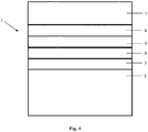
- Fig. 1 purely schematically shows a preferred embodiment of the layer system 1 according to the invention in a cross-sectional view.
- the layer system 1 comprises a substrate 2, a back electrode 3, an absorber layer 4, a first buffer layer 5, a second buffer layer 6 and a front electrode 7.
- the production process begins in the usual way with the thermal deposition of the back contact layer 3 of Mo on a glass substrate 2.
- the back electrode 3 of Mo can also be a layered electrode of a first, applied to the glass substrate SiN sublayer and a second, applied thereto Mo Partial layer can be used, which improves the properties of this back contact.
- the absorber layer 4 made of Cu (In, Ga) (S, Se) 2 is deposited on the back electrode 3.
- the first buffer layer 5 of In 2 (S 1 -x, Se x ) 3 + ⁇ , the second buffer layer 6 of undoped ZnO, and then a front electrode 7 of ZnO doped with aluminum are produced.
- the back electrode 3 made of molybdenum has a layer thickness of 400 nm.
- the absorber layer 4 is made with a thickness of 1.5 microns with the AVANCIS RTP process.
- the surface of the absorber layer 4 has an anion composition [S] / ([Se] + [S]) of about 35%.
- the gallium concentration is below 1% at the surface.
- the In 2 (S 1 -x, Se x ) 3 + ⁇ buffer layer 5 was thermally evaporated in a high vacuum.
- the selenium content of the buffer layer x is 0 to 3%.
- the stoichiometric deviation ⁇ is about -0.1 (which corresponds to an In 2 S 2.9 ).
- the layer thickness of the first buffer layer is 80 nm.
- 60 nm undoped ZnO is deposited by an RF sputtering process.
- the front electrode is 1200 nm ZnO: Al deposited with DC magnetron sputtering.
- the process temperatures during deposition of the absorber layer 4 and the subsequent layers 5, 6, 7 are well below 150 ° C, namely 70 ° C.
- Fig. 2 is the efficiency distribution of 32 solar cells, which are simultaneously applied together on a glass substrate of size 10 x 10 cm 2 (aperture area 1.4 cm 2 ), shown in three dimensions.
- These 32 solar cells include the above layer system according to the invention and have an average efficiency of 13.2%. The maximum value is 14.0%.
- Fig. 3 and Fig. 4 The results of Raman spectroscopy studies on finished solar cell devices are in Fig. 3 and Fig. 4 shown. These Raman spectra were performed at room temperature with an argon ion excitation laser at a wavelength of 488 nm for each one solar cell with an amorphous ( Figure 3 ) and a crystalline In 2 (S 1-x , Se x ) 3 + ⁇ - layer ( Figure 4 ).
- the crystalline In 2 (S 1 -x , Se x ) 3 + ⁇ layer is characterized by a structured spectrum in which the single lines are clearly visible at the positions of the spectrum of ⁇ -In 2 S 3 .
- the observed Raman modes can be assigned to the contributing phases CuInSe 2 , CuInS 2 , In 2 S 3 and ZnO as follows: the line at 179 cm -1 and the adjacent side modems at 210 to 220 cm -1 of the phase CuInSe 2 , the line at 190 cm -1 of the phase CuInS 2 , the lines at 189, 244, 266, 306, 326 and 367 cm -1 of the phase In 2 S 3 and the lines at 430 and 570 cm -1 including the Flank towards smaller wavenumbers towards the phase ZnO.
- This layer shows the diffractogram of cubic In 2 S 3 by X-ray diffraction (XRD), which also proves the crystalline nature of the sample.
- XRD X-ray diffraction
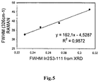
- Fig. 5 the relationship between the Raman line width of the peak at 326 cm -1 and the linewidth of the XRD (111) reflection of In 2 (S 1-x , Se x ) 3 + ⁇ layers is shown.
- the width of the Raman lines correlates well with the width of the (111) reflection from the X-ray diffraction pattern. The wider the line of the (111) reflection, the broader the Raman line and the more amorphous the structure of the sample.
- the established relationship between the two line widths is also given by formula.
- the width of the Raman line was determined by fitting Gauss-Lorentz lines to the plotted line positions of In 2 S 3 .
- Fig. 6 again shows the relationship between Raman line width of the peak at 326 cm -1 and efficiency for the In 2 (S 1 -x, Se x ) 3 + ⁇ layers. It can be seen that the broader the Raman line, ie the more amorphous the structure, the higher the efficiency of the layers. This means that very good solar cells, ie cells with a high degree of efficiency, are characterized by an unstructured Raman spectrum, a greatly broadened Raman line and the absence of crystalline X-ray diffraction reflections of the indium sulfide layer in the process parameters and the absorbers used here. In Fig. 6 Also, the established relationship between the Raman line width of the peak at 326 cm -1 and efficiency is given by formula. For strongly amorphous layers, the determination of the line width becomes inaccurate. The layers with completely unstructured spectrum lead to the best solar cell efficiencies.
Description
- Die vorliegende Erfindung betrifft ein Schichtsystem für DünnschichtSolarzellen gemäß dem Oberbegriff des Anspruchs 1 und Solarzellen oder Solarzellenmodule mit diesem Schichtsystem.
- Dünnschichtsysteme für Solarzellen und Solarmodule sind hinreichend bekannt und in verschiedenen Ausführungen, je nach Substrat und aufgebrachten Materialien, auf dem Markt vorhanden. Die Materialien werden so gewählt, dass das einfallende Sonnenspektrum maximal ausgenutzt wird. Derzeitig sind Dünnschichtzellen aus Halbleitermaterialien kommerziell erhältlich, beispielsweise aus Cadium-Tellurid (CdTe), oder Kupfer-Indium(Gallium)-Schwefel-Selen-Verbindungen (Cu(In/Ga)(Se/S)), bekannt als CIS- bzw. CIGS-Zellen, wobei hier je nach Zelltyp S für Schwefel und/oder für Selen stehen kann. Am häufigsten wird amorphes Silizium (a:Si:H) für Dünnschichtzellen verwendet. Inzwischen erreichen CIS-Dünnschichtzellen die annähernd die gleichen Wirkungsgrade wie Module aus multikristallinem Silizium.
- Aktuelle Dünnschichtsolarzellen und Solarmodule auf Basis von Cu(In,Ga)(S,Se)2 benötigen eine Pufferschicht zwischen p-leitendem Cu(In,Ga)(S,Se)2-Absorber und n-leitender Frontelektrode, die üblicherweise Zinkoxid (ZnO) umfasst. Nach derzeitiger Erkenntnis ermöglicht diese Pufferschicht eine elektronische Anpassung zwischen Absorbermaterial und Frontelektrode. Sie bietet außerdem einen Schutz vor Sputterschäden im nachfolgenden Prozessschritt der Abscheidung der Frontelektrode durch DC-MagnetronSputtern. Zusätzlich verhindert sie durch Aufbau einer hochohmigen Zwischenschicht zwischen p- und n-Halbleiter den Stromabfluss von elektronisch guten in schlechte Bereiche.
- Bisher wurde am häufigsten Kadmiumsulfid (CdS) als Pufferschicht verwendet. Um gute Wirkungsgrade der Zelle erzeugen zu können, wurde CdS bisher in einem CBD-Prozess (chemischer Badprozess) nasschemisch abgeschieden. Damit ist allerdings der Nachteil verbunden, dass der nasschemische Prozess nicht gut in den Prozessablauf der gegenwärtigen Produktion von Cu(In,Ga)(S,Se)2-Dünnschichtsolarzellen passt.
- Ein weiterer Nachteil der CdS-Pufferschicht besteht darin, dass sie das toxische Schwermetall Kadmium enthält. Dadurch entstehen höhere Produktionskosten, da erhöhte Sicherheitsvorkehrungen im Produktionsprozess, z.B. bei der Entsorgung des Abwassers, getroffen werden müssen. Die Entsorgung des Produktes kann auch unter Umständen für den Kunden höhere Kosten verursachen, da der Hersteller je nach örtlicher Gesetzgebung zur Rücknahme, zur Entsorgung oder zum Recycling des Produktes gezwungen werden könnte und die dadurch entstehenden Kosten an die Kunden weitergeben würde.
- Es wurden daher verschiedene Alternativen zum Puffer aus CdS für unterschiedliche Absorber aus der Familie der Cu(In,Ga)(S,Se)2-Halbleiter getestet; beispielsweise gesputtertes ZnMgO, durch CBD abgeschiedenes Zn(S,OH), durch CBD abgeschiedenes In(O,OH) und Indiumsulfid, abgeschieden durch ALD (A-tomicLayer Deposition), ILGAR (Ion Layer Gas Deposition), Spray Pyrolose oder PVD (Physical Vapor Deposition)-Verfahren, wie z.B. thermisches Verdampfen oder Sputtern.
- Allerdings eignen sich diese Materialien noch nicht als Puffer für die Solarzellen auf Basis von Cu(In,Ga)(S,Se)2 für eine kommerzielle Nutzung, da sie nicht die gleichen Wirkungsgrade (Verhältnis von eingestrahlter Leistung zur erzeugten elektrischen Leistung einer Solarzelle) erreichen, wie solche mit einer CdS-Pufferschicht, die etwa bis nahezu 20 % für Laborzellen auf kleinen Flächen sowie zwischen 10% und 12% für großflächige Module liegen. Weiterhin zeigen sie zu große Instabilitäten, Hystereseeffekte oder Degradationen im Wirkungsgrad, wenn sie Licht, Wärme und/oder Feuchte ausgesetzt sind.
- Ein weiterer Nachteil von CdS liegt darin begründet, dass CdS ein direkter Halbleiter mit einer direkten elektronischen Bandlücke von etwa 2.4 eV ist und daher in einer Cu(In,Ga)(S,Se)2/CdS/ZnO-Solarzelle schon bei CdS-Schichtdicken von einigen 10 nm das einfallende Licht absorbiert wird. Da es in diesem Bereich des Heteroübergangs und im Puffermaterial viele Kristalldefekte, d.h. Rekombinationszentren gibt, rekombinieren die erzeugten Ladungsträger in dieser Schicht gleich wieder. Damit geht das in der Pufferschicht absorbierte Licht für die elektrische Ausbeute verloren, d.h. der Wirkungsgrad der Solarzelle wird kleiner, was für eine Dünnschichtzelle nachteilig ist.
- LOKHANDE CD ET AL: "Chemical bath deposition of indium sulphide thin films: preparation and characterization"THIN SOLID FILMS, ELSEVIER-SEQUOIA S.A. LAUSAN-NE, CH LNKD- DOI: 10.1016/S0040-6090(98)00980-8, Bd. 340, Nr. 1-2, 26. Februar 1999 (1999-02-26), Seiten 18-23, und QASRAWI ET AL: "Temperature dependence of the band gap, refractive index and single-oscillator parameters of amorphous indium selenide thin films"OPTICAL MATERIALS, ELSEVIER SCIENCE PUBLISHERS B.V. AMS-TERDAM, NL, Bd. 29, Nr. 12, 23. Juni 2007 (2007-06-23), Seiten 1751-1755 zeigen jeweils ein Schichtsystem gemäß dem Oberbegriff von Patentanspruch 1.
- Aufgabe der vorliegenden Erfindung ist es daher, ein Schichtsystem auf Basis von Cu(In,Ga)(S,Se)2 für Solarzellen oder Solarmodule mit einer Pufferschicht bereitzustellen, das einen hohen Wirkungsgrad und hohe Stabilität aufweist, wobei die Herstellung kostengünstig und umweltverträglich sein soll. Diese Aufgabe wird erfindungsgemäß durch ein Schichtsystem gemäß Anspruch 1 und eine Solarzelle oder ein Solarzellenmodul nach Anspruch 9 gelöst. Vorteilhafte Weiterbildungen der Erfindung ergeben sich aus den Unteransprüchen.
- Das Schichtsystem umfasst eine Absorberschicht aus einem Verbindungshalbleitermaterial mit Chalkopyritstruktur (Cu(In,Ga)(S1-y,Sey)2, wobei 0 ≤ y ≤ 1 gilt) und eine erste Pufferschicht, wobei die erste Pufferschicht In2(S1-x,Sex)3+δ (Indiumsulfidselenid) umfasst und 0 ≤ x ≤ 1 gilt. Die In2(S1-x, Sex)3+δ-Pufferschicht ist weiterhin amorph ausgebildet.
- Die mit diesem Schichtsystem hergestellten Solarzellen zeigen hohe Wirkungsgrade bei gleichzeitig hoher Langzeitstabilität. Da nunmehr keine toxischen Substanzen mehr zum Einsatz kommen, ist das Herstellungsverfahren umweltschonender und billiger und es entstehen auch keine Nachfolgekosten, wie bei CdS-Pufferschichten.
- Im Einzelnen hat sich überraschend gezeigt, dass mit dem erfindungsgemäßen Schichtsystem vergleichbar gute Solarzellencharakteristika erreicht werden können, wie sie bei herkömmlichen CdS-Pufferschichten vorliegen. Mit dem erfindungsgemäßen Aufbau können nämlich hohe Wirkungsgrade von 12,2% bis 14,3% erreicht werden.
- Amorph im Kontext der vorliegenden Erfindung heißt, dass bei Röntgenstrukturuntersuchungen die Signale, die eine kristalline Struktur widerspiegeln, unter der Nachweisgrenze liegen. Außerdem zeigt das Raman Spektrum (bei 488nm Anregungswellenlänge) der Schichten im Bereich von 220cm-1 und 380cm-1 Wellenzahlen eine breite Bande mit Maximum bei 290cm-1, in der keine Einzellinien mehr auflösbar sind. Bei den dieser Erfindung zu Grunde liegenden Untersuchungen hatte sich gezeigt, dass die Indiumsulfid-Schichten auf den Glassubstraten in der Regel amorph aufgewachsen waren. Auf den Absorberschichten waren sie je nach Prozessbedingungen entweder amorph oder kristallin. Überraschenderweise ergaben nur die Schichtsysteme besonders gute Wirkungsgrade größer als 12% bei denen die Indiumsulfid-Schicht auf dem Absorber amorph aufgewachsen war. Schichten mit kristallinem Indiumsulfid ergaben Wirkungsgrade zwischen 6 und 12%.
- Bevorzugt enthält die erste Pufferschicht keine Verunreinigungen, d.h. sie ist nicht absichtlich mit weiteren Elementen, wie Sauerstoff, Kohlenstoff oder Chlor versehen und enthält diese höchstens im Rahmen fertigungstechnisch nicht vermeidbarer Konzentrationen von kleiner gleich 1 Mol %. Dadurch lässt sich ein hoher Wirkungsgrad sicherstellen.
- Erfindungsgemäß liegt die als "δ" bezeichnete Abweichung von der Stöchiometrie zwischen -0,2 und 0. Es wird dabei ein Wert bevorzugt, der etwa bei δ=-0,1 liegt, da mit dieser leicht indiumreichen Zusammensetzung die besten Zellen erreicht werden konnten.
- Durch die amorphe Ausbildung der ersten Pufferschicht wird der hohe Wirkungsgrad weitgehend bestimmt. Untersuchungen zeigen nämlich einen reziproken Zusammenhang zwischen Wirkungsgrad und Kristallinität für die hier verwendeten Schichten und Abscheideverfahren. Je weniger kristallin, d.h. je amorpher die Struktur ist, desto vorteilhafter ist dies für den Wirkungsgrad. Außerdem können amorphe Schichten bei geringeren Temperaturen hergestellt werden, wodurch eine massive Interdiffusion der Elemente zwischen Puffer und Absorber vermieden werden und die Herstellung allgemein erleichtert wird. Amorphe Halbleiterschichten werden in Solarzellen bisher nur bei amorphen Silizium-Germanium Schichtsystemen sowie bei Heteroübergängen aus kristallinen und amorphen Silizium verwendet. Für Chalkopyrithalbleiter sind Kombinationen mit amorphen Puffer oder amorphen Frontelektroden bisher nicht bekannt.
- Ein weiterer Vorteil des erfindungsgemäßen Schichtsystems besteht darin, dass die Zellen eine höhere Stabilität gegen Temperatur, Licht, Feuchtigkeit, sowie mechanische und elektrische Spannung aufweisen. Bei den bisherigen Solarzellen auf Chalkopyritbasis werden nämlich oft Hystereseffekte beobachtet: der Wirkungsgrad kann durch Einwirkung von Wärme und/oder Feuchtigkeit degradiert werden. Durch Beleuchtung kann zwar der Wirkungsgrad teilweise wieder hergestellt werden. Im ungünstigen Fall bleiben jedoch irreversible Verluste. In manchen Fällen stellt sich der Wirkungsgrad nach Herstellung der Zellen erst durch lange Beleuchtung (Light Soaking) ein. Bei den mit dem erfindungsgemäßen Schichtsystem hergestellten Solarzellen zeigen die Messungen des Alterungseffekts unter feuchter Hitze (85% relative Feuchtigkeit, 85 °C Temperatur) dagegen, dass sich die unverkapselten oder verkapselten Zellen gleich oder besser als solche mit CdS-Pufferschicht und ZnO-Frontelektrode verhalten. Die Lichtexposition von erfindungsgemäßen Zellen verursacht auch wenig Änderung des Wirkungsgrades, nämlich weniger als 5%, was eine merkliche Verbesserung der Stabilität des Schichtsystems ist.
- Aus Messungen der optischen Transmission als Funktion der Wellenlänge von In2(S1-x,Sex)3+δ-Schichten auf Glas wurde mit Hilfe von Tauc Plots festgestellt, dass die Bandlücke EG der ersten Pufferschicht zwischen 2,0 und 2,2 eV liegt. Diese Bandlücke ist zwar kleiner als die von CdS, jedoch ist CdS ein direkter Halbleiter, während die Auswertung der Tauc Plots zeigten, das die verwendeten In2(S1-x,Sex)3+δ-Schichten eine direkt und verbotene oder indirekte Natur der Bandlücke aufweisen, wodurch eine geringere Absorption des Lichtes in der Pufferschicht bei vergleichbaren Schichtdicken möglich ist. Eine geringere optische Absorption führt jedoch höheren Wirkungsgrad für die Umwandlung von Licht in elektrische Leistung.
- Bevorzugt liegt der Selengehalt x zwischen 0 und 0,5, bevorzugt zwischen 0 und 0,1. Minimale Selengehalte x können zweckmäßig sein, z. B. mit x = 0,08, x = 0,05, x = 0,03, x = 0,01 oder x = 0,001. Der Selengehalt kann tatsächlich auch x = 0 sein. Durch die Variation des Selengehalts kann die Bandlücke der ersten Pufferschicht und deren Bandanpassung zur Absorberschicht aus Cu(In,Ga)(S,Se)2 erfolgen, wobei bei diesen Selengehalten der Wirkungsgrad am höchsten ist. Durch die Einstellung des Selengehalts ist also eine Feinabstimmungen der Bandlücke und der Bandanpassung gegenüber In2(S1-x,Sex)3+δ möglich, wodurch der Wirkungsgrad zusätzlich erhöht werden kann.
- Erfindungsgemäß umfasst die Absorberschicht Cu(In,Ga)(S,Se)2 mit einem Verhältnis der molaren Konzentrationen [S]/([Se]+[S]) an der Oberfläche der Absorberschicht zwischen 20% bis 60%, und bevorzugt 35%, wodurch der Schwefel in das Anionengitter der Chaclopyritstruktur eingebaut wird. Auch hierdurch lässt sich eine Feinabstimmung der Bandlücke und der Bandanpassung gegenüber In2(S1-x,Sex)3+δ erzielen.
- Es lässt sich feststellen, dass die Kombination der Pufferschicht mit der Absorberschicht von der richtigen Einstellung des Schwefelgehaltes im Absorber und des Selengehaltes im Puffer abhängt. In diesem zusätzlichen Freiheitsgrade liegt ein weiterer Vorteil dieser Erfindung. Zum Einstellen der optimalen elektronischen Struktur am Heteroübergang sind keine hohen Temperaturen zur Herbeiführung der richtigen Zusammensetzung durch Interdiffusion notwendig.
- Erfindungsgemäß weist die Schwefel-Konzentration im Absorber einen abfallenden Gradienten von der Oberfläche, also der zur ersten Pufferschicht weisenden Grenzfläche, zum Inneren des Absorbers auf, wodurch der Wirkungsgrad ebenfalls positiv beeinflusst wird. Der Schwefelgradient kann beim Herstellungsprozess der CIS Absorber durch den Selenierungs- und Sulfurisierungsprozess von metallischen Schichten durch geeignete Temperatur- und Gaszeitprofile eingestellt werden. Das molare Verhältnis S/(Se+S) nimmt von der Oberfläche von 20% bis 60% auf Werte um 5-10% im Inneren der Absorberschicht ab, so dass das Verhältnis S/(Se+S) integral deutlich geringer ist, als an der Oberfläche. Zum Rückkontakt hin kann das Verhältnis S/(Se+S) auch wieder zunehmen. Der Gradient des Schwefels führt zu einem Gradienten in der Bandlücke. Dass ein fallender Gradient der Bandlücke in der Basis einer Solarzelle zu verbesserten Wirkungsgraden führen kann, ist aus verschiedenen Solarzellentechnologien bekannt. In der erfindungsgemäßen Kombination mit der amorphen Indiumsulfidschicht erlaubt der Gradient jedoch zusätzlich eine Anpassung der Bandstrukturen am Heteroübergang des Indiumsulfid/Cu(In,Ga)(S,Se)2-Schichtsystems.
- Vorteilhaft ist die In2(S1-x,Sex)3+δ-Schicht zwischen 10 nm und 200 nm, insbesondere zwischen 40 nm und 140 nm, bevorzugt 60 nm dick, da hierdurch die Lichtabsorption durch die In2(S1-x, Sex)3+δ-Pufferschicht gering ist.
- Vorteilhaft umfasst das erfindungsgemäße Schichtsystem eine zweite Pufferschicht, die bevorzugt zwischen der ersten Pufferschicht und einer Frontelektrode angeordnet ist. Vorzugsweise umfasst die auf der ersten Pufferschicht aufgebrachte zweite Pufferschicht undotiertes Zn1-zMgzO, wobei 0 ≤ z ≤ 1 ist. Ihre Schichtdicke beträgt zweckmäßig bis zu 200 nm, insbesondere 20 nm bis 140 nm, bevorzugt 60 nm.
- Vorteilhaft ist eine Frontelektrode vorgesehen, die ein transparentes leitendes Oxid (TCO) umfasst. Insbesondere umfasst sie Indiumzinnoxid (ITO) und/oder ZnO, wobei dotiertes ZnO, insbesondere Al- oder Ga-dotiertes ZnO bevorzugt werden.
- Als Träger in dem erfindungsgemäßen Schichtsystem ist vorzugsweise ein Metall, Glas-, Kunststoff oder Keramiksubstrat vorgesehen, wobei Glas bevorzugt wird. Es können aber auch andere transparente Trägermaterialien, insbesondere Kunststoffe verwendet werden.
- Unter dem Absorber ist vorzugsweise eine Rückelektrode, z.B. Molybdän (Mo) oder andere Metalle umfassend, vorgesehen. In einer vorteilhaften Ausgestaltung der Rückelektrode weist diese eine Molybdänteilschicht auf, die an den Absorber angrenzt, und eine Siliziumnitridteilschicht (SiN), die an die Mo-Teilschicht angrenzt.
- Unabhängiger Schutz wird für Solarzellen mit dem erfindungsgemäßen Schichtsystem und für Solarzellenmodule beansprucht, die diese Solarzellen beinhalten.
- Zweckmäßig erfolgt das Verfahren zur Herstellung eines solchen Schichtsystems so, dass zumindest die Abscheidung der ersten Pufferschicht im Vakuum erfolgt, wobei bevorzugt die Erzeugung des gesamten Schichtsystems im Vakuum erfolgt.
- Ein Vorteil dieses Vakuumprozesses besteht darin, dass dadurch zum einen eine höhere Materialausbeute erzielt wird. Außerdem ist er im Gegensatz zur Nassabscheidung umweltverträglicher, da im Gegensatz beispielsweise zur chemischen Badabscheidung einer Pufferschicht aus CdS keine kontaminierten Abwässer erzeugt werden. Schließlich können verschiedene Vakuumprozesse, wie auch die Herstellung der zweiten undotierten ZnO-Pufferschicht oder der dotierten ZnO-Frontelektrode in einer Anlage verbunden werden, wodurch die Herstellung preiswerter erfolgen kann. Je nach Ausgestaltung des Prozesses zur Herstellung des Absorbers ist auch eine Kombination mit dem Absorberprozess ohne Luftexposition denkbar.
- Ein weiterer Vorteil besteht darin, dass durch das Vakuumverfahren der Einbau von Sauerstoff oder Hydroxid verhindert wird. Hydroxid-Komponenten in der Pufferschicht stehen nämlich im Verdacht, verantwortlich für Transienten des Wirkungsgrades bei Einwirkung von Wärme und Licht zu sein.
- Vorteilhaft erfolgt die Aufbringung der Pufferschicht bei Temperaturen kleiner gleich 150 °C, insbesondere kleiner gleich 130 °C und bevorzugt zwischen 50°C und 100 °C. Dadurch können die Kosten der Vakuumanlage gesenkt werden. Im Gegensatz dazu müssen beispielsweise Indiumsulfidpuffer auf Cu(In,Ga)Se2, das keinen Schwefel umfasst, entweder bei Temperaturen höher als 150 °C abgeschieden werden oder der gesamte Zellenaufbau muss nach Abscheidung der ZnO-Frontelektrode bei höheren Temperaturen getempert werden. In der vorliegenden Erfindung sind Temperaturen für die Herstellung der Schicht deutlich kleiner als 150 °C möglich und der Zellenaufbau muss nicht nachgetempert werden. Dies könnte darin begründet liegen, dass die schwefelhaltige Oberfläche von Cu(In,Ga)(S,Se)2 im erfindungsgemäßen Absorber/Puffer-Schichtaufbau bereits die richtige Bandanpassung zum Puffer besitzt.
- Zweckmäßig wird die Absorberschicht in einem Avancis RTP- ("rapid thermal processing") Prozess aufgebracht. Dabei werden zunächst einer Vorläuferschicht auf das Substrat mit Rückelektrode abgeschieden: die Elemente Cu, In und Ga werden durch Sputtern sowie amorphes Selen durch thermisches Verdampfen aufgebracht. Bei diesen Prozessen liegt die Substrattemperatur unter 100°C, so dass die Schichten im wesentlichen als Metalllegierung plus elementares Selen unreagiert erhalten blieben. Anschließend wird diese Vorläuferschicht in einem schnellen Temperverfahren (RTP rapid thermal processing) in schwefelhaltiger Atmosphäre zum Cu(In,Ga)(S,Se)2 Chalcopyrithalbleiter reagiert.
- Vorteilhaft wird die erste Pufferschicht thermisch im Hochvakuum verdampft, wobei die Prozessbedingungen bevorzugt so gewählt werden, dass diese Pufferschicht auf der Absorberschicht amorph abgeschieden wird. Wesentlich für das erfindungsgemäße Schichtsystem ist also das Aufwachsen der amorphen Schicht auf dem polykristallinen Absorber. Da dünne Schichten auf unterschiedlichen Substraten verschieden aufwachsen, ist ein Nachweis nur auf dem eigentlichen Schichtsystem Absorber/Puffer oder in der vollständigen Solarzelle, nicht jedoch auf Zeugengläser (Kontrollproben), über Röntgenbeugung im streifenden Einfall und mittels Ramanspektroskopie möglich. Denkbar ist auch, dass sowohl die erste als auch die zweite Pufferschicht, wenn eine solche zum Einsatz kommt, mittels Hochfrequenzsputtern (RF-Sputtern) aufgebracht werden. Die Frontelektrode wird wiederum vorzugsweise in einem DC-Magnetronsputterverfahren aufgebracht.
- Weitere Einzelheiten und Vorteile der vorliegenden Erfindung ergeben sich aus der nachfolgenden Beschreibung im Zusammenhang mit den Zeichnungen. Dabei zeigen:
- Fig.l
- eine schematische Querschnittansicht des erfindungsgemäßen Schichtsystems,
- Fig. 2
- eine graphische Darstellung der Wirkungsgradverteilung von 32 Zellen mit Indiumsulfidselenid-Puffer,
- Fig. 3
- Ergebnisse der Ramanspektroskopie (vertikale Achse) an einer Dünnschichtzelle mit einer amorphen Indiumsulfidselenid-Pufferschicht (horizontale Achse),
- Fig. 4
- Ergebnisse der Ramanspektroskopie (vertikale Achse) an einer Dünnschichtzelle mit einer kristallinen Indiumsulfidselenid-Pufferschicht (horizontale Achse), wobei zusätzlich berechnete Linen an den Positionen der CuInSe2-, CuInS2-, ZnO- und In2S3-Phasen eingezeichnet sind,
- Fig. 5
- die Korrelation zwischen Raman-Linienbreite des Peaks bei 326 cm-1 (vertikale Achse) und Linienbreite des (111)-Reflexes von kubischem Indiumsulfidselenid (horizontale Achse) und
- Fig. 6
- den Zusammenhang zwischen Raman-Linienbreite des Peaks bei 326 cm-1 (horizontal Achse) und Wirkungsgrad (vertikale Achse).
- Anhand der
Fig. 1 wird nachfolgend zunächst auf das erfindungsgemäße Schichtsystem und sein Herstellungsverfahren eingegangen. -
Fig. 1 zeigt rein schematisch ein bevorzugtes Ausführungsbeispiel des erfindungsgemäßen Schichtsystems 1 in einer Querschnittsansicht. Das Schichtsystem 1 umfasst ein Substrat 2, eine Rückelektrode 3, eine Absorberschicht 4, eine erste Pufferschicht 5, eine zweite Pufferschicht 6 und eine Frontelektrode 7. - Das Herstellungsverfahren beginnt in üblicher Weise mit der thermischen Abscheidung der Rückkontaktschicht 3 aus Mo auf einem Glassubstrat 2. Statt der Rückelektrode 3 aus Mo kann auch eine geschichtete Elektrode aus einer ersten, auf dem Glassubstrat aufgebrachten SiN-Teilschicht und einer zweiten, darauf aufgebrachten Mo-Teilschicht verwendet werden, was die Eigenschaften dieses Rückkontakts verbessert. In einem weiteren Schritt wird die Absorberschicht 4 aus Cu(In,Ga)(S,Se)2 auf der Rückelektrode 3 aufgebracht. In weiteren Schritten werden dann die erste Pufferschicht 5 aus In2(S1-x,Sex)3+δ, die zweite Pufferschicht 6 aus undotiertem ZnO und anschließend eine Frontelektrode 7 aus ZnO dotiert mit Aluminium hergestellt.
- Folgende Parameter werden dabei verwendet. Die Rückelektrode 3 aus Molybdän weist eine Schichtdicke von 400 nm auf. Die Absorberschicht 4 wird mit einer Dicke von 1,5 µm mit dem AVANCIS RTP-Prozess hergestellt. Die Oberfläche der Absorberschicht 4 weist eine Anionenzusammensetzung [S]/([Se]+[S]) von etwa 35% auf. Die Galliumkonzentration liegt an der Oberfläche unter 1%. Die In2(S1-x,Sex)3+δ-Pufferschicht 5 wurde thermisch im Hochvakuum verdampft. Der Selengehalt der Pufferschicht x liegt bei 0 bis 3%. Die Stöchiometrieabweichung δ beträgt etwa -0,1 (das entspricht einer In2S2.9). Die Schichtdicke der ersten Pufferschicht beträgt 80 nm. Als zweite Pufferschicht wird 60 nm undotiertes ZnO durch einen RF-Sputterprozess abgeschieden. Als Frontelektrode wird 1200 nm ZnO:Al mit DC-Magnetronsputtern abgeschieden. Die Prozesstemperaturen bei Abscheidung der Absorberschicht 4 und der nachfolgenden Schichten 5, 6, 7 betragen deutlich unter 150 °C, nämlich 70°C.
- In
Fig. 2 ist die Wirkungsgradverteilung von 32 Solarzellen, die gleichzeitig zusammen auf einem Glassubstrat der Größe 10 x 10 cm2 (Aperturfläche 1,4 cm2) aufgebracht sind, dreidimensional dargestellt. Diese 32 Solarzellen beinhalten das obige erfindungsgemäße Schichtsystem und weisen einen Mittelwert des Wirkungsgrades von 13,2% auf. Der maximale Wert liegt bei 14,0%. - Die Ergebnisse von Ramanspektroskopie-Untersuchungen an fertigen Solarzellen-Bauelementen sind in
Fig. 3 undFig. 4 dargestellt. Diese Ramanspektren wurden bei Raumtemperatur mit einem Argonionen-Anregungslaser bei einer Wellenlänge von 488 nm für jeweils eine Solarzelle mit einer amorphen (Fig.3 ) und einer kristallinen In2(S1-x,Sex)3+δ-Schicht (Fig.4 ) gemessen. Die kristalline In2(S1-x,Sex)3+δ-Schicht zeichnet sich durch ein strukturiertes Spektrum aus, in dem die Einzellinien an den Positionen des Spektrums von β-In2S3 gut erkennbar sind. Die beobachteten Ramanmoden können den beitragenden Phasen CuInSe2, CuInS2, In2S3 und ZnO wie folgt zugeordnet werden: die Linie bei 179 cm-1 und die benachbarten Nebenmodem bei 210 bis 220 cm-1 der Phase CuInSe2, die Linie bei 190 cm-1 der Phase CuInS2, die Linien bei 189, 244, 266, 306, 326 und 367 cm-1 der Phase In2S3 und die Linien bei 430 und 570 cm-1 inklusive der Flanke zu kleineren Wellenzahlen hin der Phase ZnO. Diese Schicht zeigt bei Röntgenbeugung (XRD) das Diffraktogramm von kubischem In2S3, was die kristalline Natur der Probe ebenfalls beweist. Bei der amorphen In2(S1-x,Sex)3+δ-Schicht inFig. 3 dagegen ist im Ramanspektrum ein unstrukturierter Berg in dem Wellenzahlenbereich zu sehen, in dem auch die Signale des kristallinen Indiumsulfids liegen, insbesondere im Bereich von 220 bis 380 cm-1. Für diese Probe sind auch keine Reflexe in der Röntgenbeugung zu erkennen, die einer Indiumsulfid-Phase zugeordnet werden könnten. - In
Fig. 5 ist der Zusammenhang zwischen Ramanlinienbreite des Peaks bei 326 cm-1 und Linienbreite des XRD (111) Reflexes von In2(S1-x,Sex)3+δ-Schichten dargestellt. In den Fällen, wo Indiumsulfidreflexe im Diffraktogramm zu erkennen sind, korreliert die Breite der Ramanlinien gut mit der Breite des (111)-Reflexes aus dem Röntgenbeugungsdiffraktogramm. Je breiter die Linie des (111)-Reflexes ist, desto breiter ist die Ramanlinie und desto amorpher ist die Struktur der Probe. InFig. 5 ist auch der ermittelte Zusammenhang zwischen beiden Linienbreiten formelmäßig angegeben. Die Breite der Ramanlinie wurde durch Anpassung von Gauß-Lorentzlinien an den eingezeichneten Linienpositionen von In2S3 bestimmt. -
Fig. 6 zeigt wiederum den Zusammenhang zwischen Ramanlinienbreite des Peaks bei 326 cm-1 und Wirkungsgrad für die In2(S1-x,Sex)3+δ-Schichten. Zu erkennen ist, dass je breiter die Ramanlinie, d.h. je amorpher die Struktur ist, der Wirkungsgrad der Schichten desto höher ist. Das bedeutet, dass sehr gute Solarzellen, d.h. Zellen mit einem hohen Wirkungsgrad, bei den hier untersuchten Prozessparametern und den verwendeten Absorbern sich durch ein unstrukturiertes Ramanspektrum, stark verbreiterte Ramanlinie und das Fehlen von kristallinen Röntgenbeugungsreflexen der Indiumsulfidschicht auszeichnen. InFig. 6 ist auch der ermittelte Zusammenhang zwischen der Ramanlinienbreite des Peaks bei 326 cm-1 und Wirkungsgrad formelmäßig angegeben. Bei stark amorphen Schichten wird die Bestimmung der Linienbreite ungenau. Die Schichten mit gänzlich unstrukturiertem Spektrum führen zu den besten Solarzellenwirkungsgraden. - Aus den vorstehenden Ausführungen ist klar geworden, dass durch die vorliegende Erfindung die Nachteile von bisher verwendeten CdS-Pufferschichten bzw. den alternativen Pfufferschichten bei Dünnschichtsolarzellen überwunden werden konnten, wobei der Wirkungsgrad und die Stabilität der damit erzeugten Solarzellen ebenfalls sehr gut ist. Gleichzeitig ist das Herstellungsverfahren kostengünstig, effektiv und umweltschonend.
Claims (9)
- Schichtsystem (1) für Dünnschichtsolarzellen, das eine Absorberschicht (4) und eine erste Pufferschicht (5) umfasst, wobei die Absorberschicht (4) auf der Basis eines Cu(In,Ga)(S1-y,Sey)2-Verbindungshalbleitermaterials gebildet ist, wobei 0 ≤ y ≤ 1 gilt, wobei die erste Pufferschicht (5) amorph ist und die erste Pufferschicht (5) In2(S1-x,Sex)3+δ umfasst, wobei 0 ≤ x ≤ 1 gilt, dadurch gekennzeichnet, dass die Abweichung δ von der Stöchiometrie zwischen -0,2 und 0 liegt, und das Verhältnis der molaren Konzentrationen [S]/([Se]+[S]) an der der ersten Pufferschicht (5) zugewandten Oberfläche der Absorberschicht (4) von 20% bis 60% beträgt und auf Werte von 5% bis 10% im Innern der Absorberschicht abnimmt.
- Schichtsystem (1) gemäß Anspruch 1, dadurch gekennzeichnet, dass der Selengehalt 0 ≤ x ≤ 0,5, bevorzugt 0 ≤ x ≤ 0,1 beträgt.
- Schichtsystem (1) gemäß Anspruch 1 oder 2, dadurch gekennzeichnet, dass das Verhältnis der molaren Konzentrationen [S]/([Se]+[S]) an der der ersten Pufferschicht (5) zugewandten Oberfläche der Absorberschicht (4) 35% beträgt.
- Schichtsystem (1) gemäß einem der vorherigen Ansprüche, dadurch gekennzeichnet, dass die Schichtdicke der ersten Pufferschicht (5) zwischen 10 nm und 200 nm liegt, insbesondere zwischen 40 nm und 140 nm, bevorzugt 80 nm.
- Schichtsystem (1) gemäß einem der vorherigen Ansprüche, dadurch gekennzeichnet, dass zusätzlich eine zweite Pufferschicht (6) vorgesehen ist, die bevorzugt auf der ersten Pufferschicht (5) angeordnet ist.
- Schichtsystem (1) gemäß Anspruch 5, dadurch gekennzeichnet, dass die zweite Pufferschicht (6) undotiertes Zn1-zMgzO umfasst, wobei 0 ≤ z ≤ 1 beträgt.
- Schichtsystem (1) gemäß Anspruch 5 oder 6, dadurch gekennzeichnet, dass die Schichtdicke der zweiten Pufferschicht bis zu 200 nm beträgt, insbesondere 10 nm bis 140 nm, bevorzugt 60 nm.
- Schichtsystem (1) gemäß einem der vorherigen Ansprüche, dadurch gekennzeichnet, dass oberhalb der ersten Pufferschicht (5) eine Frontelektrode (7) angeordnet ist, die aus einem transparenten leitenden Oxid (TCO), bevorzugt Al- oder Ga-dotiertes ZnO, besteht.
- Solarzelle oder Solarzellenmodul, gekennzeichnet durch das Schichtsystem (1) nach einem der vorherigen Ansprüche.
Applications Claiming Priority (2)
| Application Number | Priority Date | Filing Date | Title |
|---|---|---|---|
| DE102008024230A DE102008024230A1 (de) | 2008-05-19 | 2008-05-19 | Schichtsystem für Solarzellen |
| PCT/EP2009/003587 WO2009141132A2 (de) | 2008-05-19 | 2009-05-19 | Schichtsystem für solarzellen |
Publications (2)
| Publication Number | Publication Date |
|---|---|
| EP2281310A2 EP2281310A2 (de) | 2011-02-09 |
| EP2281310B1 true EP2281310B1 (de) | 2019-09-25 |
Family
ID=41212500
Family Applications (1)
| Application Number | Title | Priority Date | Filing Date |
|---|---|---|---|
| EP09749622.8A Active EP2281310B1 (de) | 2008-05-19 | 2009-05-19 | Schichtsystem für solarzellen |
Country Status (8)
| Country | Link |
|---|---|
| US (1) | US8962995B2 (de) |
| EP (1) | EP2281310B1 (de) |
| JP (1) | JP5635497B2 (de) |
| KR (1) | KR101335810B1 (de) |
| CN (1) | CN102099929B (de) |
| DE (1) | DE102008024230A1 (de) |
| ES (1) | ES2763159T3 (de) |
| WO (1) | WO2009141132A2 (de) |
Families Citing this family (23)
| Publication number | Priority date | Publication date | Assignee | Title |
|---|---|---|---|---|
| US20130112235A1 (en) * | 2010-07-28 | 2013-05-09 | Kyocera Corporation | Photoelectric conversion device, method of manufacturing photoelectric conversion device, and photoelectric conversion module |
| JP5709662B2 (ja) * | 2011-06-16 | 2015-04-30 | ソーラーフロンティア株式会社 | Czts系薄膜太陽電池の製造方法 |
| DE102012205978A1 (de) * | 2012-04-12 | 2013-10-17 | Robert Bosch Gmbh | Photovoltaische Dünnschichtsolarmodule sowie Verfahren zur Herstellung solcher Dünnschichtsolarmodule |
| WO2013189976A1 (de) | 2012-06-20 | 2013-12-27 | Saint-Gobain Glass France | Schichtsystem für dünnschichtsolarzellen |
| JP6092377B2 (ja) * | 2012-06-20 | 2017-03-08 | サン−ゴバン グラス フランスSaint−Gobain Glass France | 薄膜太陽電池用の層体 |
| JP5985052B2 (ja) | 2012-06-20 | 2016-09-06 | サン−ゴバン グラス フランスSaint−Gobain Glass France | 薄膜ソーラセル用のNaxIn1SyClzバッファ層を有する層システム |
| CN103078013B (zh) * | 2013-01-29 | 2015-05-20 | 上海交通大学 | 钒酸铋/铁酸铋异质结薄膜太阳能电池的制备方法 |
| KR101807118B1 (ko) * | 2013-03-15 | 2017-12-08 | 나노코 테크놀로지스 리미티드 | 등급 크기 및 S:Se 비율을 갖는 광전 소자 |
| JP2014187215A (ja) * | 2013-03-23 | 2014-10-02 | Kyocera Corp | 光電変換装置 |
| KR102076544B1 (ko) * | 2013-05-10 | 2020-02-12 | 에스케이이노베이션 주식회사 | 광흡수층의 제조방법 |
| JP6147926B2 (ja) * | 2013-06-27 | 2017-06-14 | サン−ゴバン グラス フランス | ナトリウムインジウム硫化物緩衝層を有する薄膜太陽電池のための層システム |
| EP2887405A1 (de) | 2013-12-23 | 2015-06-24 | Saint-Gobain Glass France | Schichtsystem für Dünnschichtsolarzellen |
| US9306098B2 (en) * | 2014-01-24 | 2016-04-05 | Tsmc Solar Ltd. | Method of making photovoltaic device comprising an absorber having a surface layer |
| US9240501B2 (en) * | 2014-02-12 | 2016-01-19 | Solar Frontier K.K. | Compound-based thin film solar cell |
| EP2947702B1 (de) * | 2014-05-21 | 2019-03-20 | AZUR SPACE Solar Power GmbH | Solarzellenstapel |
| JP2018500774A (ja) * | 2014-12-22 | 2018-01-11 | ベンブー デザイン アンド リサーチ インスティテュート フォー グラス インダストリーBengbu Design and Research Institute for Glass Industry | 硫化ナトリウムインジウム緩衝層を有する薄膜太陽電池のための層システムの製造方法 |
| US10121920B2 (en) * | 2015-06-30 | 2018-11-06 | International Business Machines Corporation | Aluminum-doped zinc oxysulfide emitters for enhancing efficiency of chalcogenide solar cell |
| TWI620335B (zh) * | 2015-08-07 | 2018-04-01 | 國立勤益科技大學 | 薄膜太陽能電池氧化鋅緩衝層結構及製程 |
| CN105261666A (zh) * | 2015-10-29 | 2016-01-20 | 厦门神科太阳能有限公司 | 薄膜太阳能电池 |
| CN107690016B (zh) * | 2017-10-23 | 2020-11-17 | 嘉兴巨腾信息科技有限公司 | 一种用于手机通讯的保护壳 |
| CN108172665A (zh) * | 2017-12-30 | 2018-06-15 | 凯盛光伏材料有限公司 | 一种cigs太阳能电池吸收层表面的处理方法 |
| EP3627564A1 (de) | 2018-09-22 | 2020-03-25 | (CNBM) Bengbu Design & Research Institute for Glass Industry Co., Ltd. | Verfahren zur nachbehandlung einer absorberschicht |
| KR20230146358A (ko) * | 2022-04-12 | 2023-10-19 | 서울대학교산학협력단 | 탠덤 태양전지 및 이의 제조방법 |
Family Cites Families (18)
| Publication number | Priority date | Publication date | Assignee | Title |
|---|---|---|---|---|
| US5141564A (en) * | 1988-05-03 | 1992-08-25 | The Boeing Company | Mixed ternary heterojunction solar cell |
| US5286306A (en) * | 1992-02-07 | 1994-02-15 | Shalini Menezes | Thin film photovoltaic cells from I-III-VI-VII compounds |
| JP3646940B2 (ja) * | 1994-11-01 | 2005-05-11 | 松下電器産業株式会社 | 太陽電池 |
| JPH1074968A (ja) * | 1996-09-02 | 1998-03-17 | Nippon Telegr & Teleph Corp <Ntt> | 太陽電池およびその製造方法 |
| JP3249407B2 (ja) * | 1996-10-25 | 2002-01-21 | 昭和シェル石油株式会社 | カルコパイライト系多元化合物半導体薄膜光吸収層からなる薄膜太陽電池 |
| JP3249408B2 (ja) * | 1996-10-25 | 2002-01-21 | 昭和シェル石油株式会社 | 薄膜太陽電池の薄膜光吸収層の製造方法及び製造装置 |
| JP3527815B2 (ja) * | 1996-11-08 | 2004-05-17 | 昭和シェル石油株式会社 | 薄膜太陽電池の透明導電膜の製造方法 |
| JPH1126790A (ja) * | 1997-07-04 | 1999-01-29 | Yazaki Corp | 半導体薄膜及びその製造方法並びに薄膜太陽電池 |
| JP2004214300A (ja) * | 2002-12-27 | 2004-07-29 | National Institute Of Advanced Industrial & Technology | ヘテロ接合を有する太陽電池 |
| CN1771610A (zh) * | 2003-04-09 | 2006-05-10 | 松下电器产业株式会社 | 太阳能电池 |
| EP1654769B2 (de) * | 2003-08-14 | 2018-02-07 | University of Johannesburg | Verfahren zur herstellung von legierungs-halbleiterfilmen der gruppe ib-iiia-via-quaternär oder höher |
| US7374963B2 (en) * | 2004-03-15 | 2008-05-20 | Solopower, Inc. | Technique and apparatus for depositing thin layers of semiconductors for solar cell fabrication |
| US7736940B2 (en) * | 2004-03-15 | 2010-06-15 | Solopower, Inc. | Technique and apparatus for depositing layers of semiconductors for solar cell and module fabrication |
| TW200633241A (en) * | 2004-11-10 | 2006-09-16 | Daystar Technologies Inc | Vertical production of photovoltaic devices |
| FR2886460B1 (fr) * | 2005-05-25 | 2007-08-24 | Electricite De France | Sulfurisation et selenisation de couches de cigs electrodepose par recuit thermique |
| DE102006039331C5 (de) * | 2006-08-15 | 2013-08-22 | Zentrum für Sonnenenergie- und Wasserstoff-Forschung Baden-Württemberg | Photovoltaik-Dünnschichtaufbau und Herstellungsverfahren |
| US8323735B2 (en) * | 2006-10-13 | 2012-12-04 | Solopower, Inc. | Method and apparatus to form solar cell absorber layers with planar surface |
| US8323408B2 (en) * | 2007-12-10 | 2012-12-04 | Solopower, Inc. | Methods and apparatus to provide group VIA materials to reactors for group IBIIIAVIA film formation |
-
2008
- 2008-05-19 DE DE102008024230A patent/DE102008024230A1/de not_active Withdrawn
-
2009
- 2009-05-19 KR KR1020107028416A patent/KR101335810B1/ko active IP Right Grant
- 2009-05-19 WO PCT/EP2009/003587 patent/WO2009141132A2/de active Application Filing
- 2009-05-19 ES ES09749622T patent/ES2763159T3/es active Active
- 2009-05-19 CN CN200980128365.XA patent/CN102099929B/zh active Active
- 2009-05-19 EP EP09749622.8A patent/EP2281310B1/de active Active
- 2009-05-19 JP JP2011509890A patent/JP5635497B2/ja active Active
- 2009-05-19 US US12/992,199 patent/US8962995B2/en active Active
Non-Patent Citations (1)
| Title |
|---|
| YOUSFI E B ET AL: "Atomic layer deposition of zinc oxide and indium sulfide layers for Cu(In,Ga)Se"2 thin-film solar cells", THIN SOLID F, ELSEVIER, AMSTERDAM, NL, vol. 387, no. 1-2, 29 May 2001 (2001-05-29), pages 29 - 32, XP004232903, ISSN: 0040-6090, DOI: 10.1016/S0040-6090(00)01838-1 * |
Also Published As
| Publication number | Publication date |
|---|---|
| US20110168258A1 (en) | 2011-07-14 |
| CN102099929B (zh) | 2014-04-30 |
| JP2011521463A (ja) | 2011-07-21 |
| JP5635497B2 (ja) | 2014-12-03 |
| WO2009141132A4 (de) | 2010-10-14 |
| DE102008024230A1 (de) | 2009-11-26 |
| EP2281310A2 (de) | 2011-02-09 |
| CN102099929A (zh) | 2011-06-15 |
| US8962995B2 (en) | 2015-02-24 |
| WO2009141132A3 (de) | 2010-08-19 |
| WO2009141132A2 (de) | 2009-11-26 |
| ES2763159T3 (es) | 2020-05-27 |
| KR101335810B1 (ko) | 2013-12-03 |
| KR20110020263A (ko) | 2011-03-02 |
Similar Documents
| Publication | Publication Date | Title |
|---|---|---|
| EP2281310B1 (de) | Schichtsystem für solarzellen | |
| EP0715358B2 (de) | Verfahren zur Herstellung einer Solarzelle mit Chalkopyrit-Absorberschicht und so hergestellte Solarzelle | |
| DE19958878B4 (de) | Dünnschicht-Solarzelle | |
| DE10010177B4 (de) | Solarzelle mit einer p-Typ Lichtabsorptionsschicht und einer Cd-freien n-Typ Schicht, die einen größeren Bandabstand und eine größere Elektronenaffinität aufweist | |
| WO2012119857A1 (de) | Verfahren zur herstellung des pentanären verbindungshalbleiters cztsse, sowie dünnschichtsolarzelle | |
| DE112011101973T5 (de) | Dünnfilm-Solarzelle | |
| DE102012100795A1 (de) | Superstrat-Solarzelle | |
| DE102011054795A1 (de) | Verfahren zum Abscheiden von Cadmiumsulfid-Schichten mittels zerstäuben zum Einsatz in photovoltaischen Dünnfilmvorrichtungen auf Cadmiumtellurid-Grundlage | |
| DE112015000755T5 (de) | Dünnfilm-Solarzelle auf Verbindungsbasis | |
| DE102012102000A1 (de) | Systeme und Verfahren zum raschen Abscheiden von Dünnfilmschichten auf Substraten von photovoltaischen Modulen | |
| EP3014652B1 (de) | Schichtsystem für dünnschichtsolarzellen mit natriumindiumsulfid-pufferschicht | |
| EP3221899B1 (de) | Schichtaufbau für eine dünnschichtsolarzelle und herstellungsverfahren | |
| WO2013020864A2 (de) | Solarmodul mit verringertem leistungsverlust und verfahren zu dessen herstellung | |
| EP2865011B1 (de) | Schichtsystem für dünnschicht-solarzellen mit einer naxinisyclz-pufferschicht | |
| EP2865001B1 (de) | Schichtsystem für dünnschichtsolarzellen | |
| DE112011102039T5 (de) | Dünnfilm-Solarzelle auf CIS-Basis | |
| EP2887405A1 (de) | Schichtsystem für Dünnschichtsolarzellen | |
| EP2865012B1 (de) | Schichtsystem für dünnschichtsolarzellen | |
| DE102013105732A1 (de) | Verfahren zum Bearbeiten einer Halbleiteranordnung | |
| EP3627564A1 (de) | Verfahren zur nachbehandlung einer absorberschicht | |
| EP0798786B1 (de) | Solarzelle mit einer Chalkopyrit-Absorberschicht | |
| WO2014207233A1 (de) | Schichtsystem für dünnschichtsolarzellen mit indiumsulfid-pufferschicht | |
| KR20180103676A (ko) | 나트륨 인듐 술피드 버퍼 층을 갖는 박층 태양 전지용 층 시스템의 제조 방법 | |
| EP2999004A1 (de) | Photoelektrische umwandlungsvorrichtung und solarzelle | |
| EP2936548B1 (de) | Verfahren zur herstellung eines verbindungshalbleiters sowie dünnschichtsolarzelle |
Legal Events
| Date | Code | Title | Description |
|---|---|---|---|
| PUAI | Public reference made under article 153(3) epc to a published international application that has entered the european phase |
Free format text: ORIGINAL CODE: 0009012 |
|
| 17P | Request for examination filed |
Effective date: 20101119 |
|
| AK | Designated contracting states |
Kind code of ref document: A2 Designated state(s): AT BE BG CH CY CZ DE DK EE ES FI FR GB GR HR HU IE IS IT LI LT LU LV MC MK MT NL NO PL PT RO SE SI SK TR |
|
| DAX | Request for extension of the european patent (deleted) | ||
| 17Q | First examination report despatched |
Effective date: 20140731 |
|
| STAA | Information on the status of an ep patent application or granted ep patent |
Free format text: STATUS: EXAMINATION IS IN PROGRESS |
|
| REG | Reference to a national code |
Ref country code: DE Ref legal event code: R079 Ref document number: 502009015972 Country of ref document: DE Free format text: PREVIOUS MAIN CLASS: H01L0031033600 Ipc: H01L0031074900 |
|
| GRAP | Despatch of communication of intention to grant a patent |
Free format text: ORIGINAL CODE: EPIDOSNIGR1 |
|
| STAA | Information on the status of an ep patent application or granted ep patent |
Free format text: STATUS: GRANT OF PATENT IS INTENDED |
|
| RIC1 | Information provided on ipc code assigned before grant |
Ipc: H01L 31/0749 20120101AFI20190307BHEP Ipc: H01L 31/032 20060101ALI20190307BHEP |
|
| INTG | Intention to grant announced |
Effective date: 20190403 |
|
| RAP1 | Party data changed (applicant data changed or rights of an application transferred) |
Owner name: (CNBM) BENGBU DESIGN & RESEARCH INSTITUTE FOR GLAS |
|
| GRAS | Grant fee paid |
Free format text: ORIGINAL CODE: EPIDOSNIGR3 |
|
| GRAA | (expected) grant |
Free format text: ORIGINAL CODE: 0009210 |
|
| STAA | Information on the status of an ep patent application or granted ep patent |
Free format text: STATUS: THE PATENT HAS BEEN GRANTED |
|
| AK | Designated contracting states |
Kind code of ref document: B1 Designated state(s): AT BE BG CH CY CZ DE DK EE ES FI FR GB GR HR HU IE IS IT LI LT LU LV MC MK MT NL NO PL PT RO SE SI SK TR |
|
| REG | Reference to a national code |
Ref country code: GB Ref legal event code: FG4D Free format text: NOT ENGLISH |
|
| REG | Reference to a national code |
Ref country code: CH Ref legal event code: EP |
|
| REG | Reference to a national code |
Ref country code: AT Ref legal event code: REF Ref document number: 1184684 Country of ref document: AT Kind code of ref document: T Effective date: 20191015 |
|
| REG | Reference to a national code |
Ref country code: IE Ref legal event code: FG4D Free format text: LANGUAGE OF EP DOCUMENT: GERMAN |
|
| REG | Reference to a national code |
Ref country code: DE Ref legal event code: R096 Ref document number: 502009015972 Country of ref document: DE |
|
| REG | Reference to a national code |
Ref country code: NL Ref legal event code: MP Effective date: 20190925 |
|
| PG25 | Lapsed in a contracting state [announced via postgrant information from national office to epo] |
Ref country code: FI Free format text: LAPSE BECAUSE OF FAILURE TO SUBMIT A TRANSLATION OF THE DESCRIPTION OR TO PAY THE FEE WITHIN THE PRESCRIBED TIME-LIMIT Effective date: 20190925 Ref country code: LT Free format text: LAPSE BECAUSE OF FAILURE TO SUBMIT A TRANSLATION OF THE DESCRIPTION OR TO PAY THE FEE WITHIN THE PRESCRIBED TIME-LIMIT Effective date: 20190925 Ref country code: BG Free format text: LAPSE BECAUSE OF FAILURE TO SUBMIT A TRANSLATION OF THE DESCRIPTION OR TO PAY THE FEE WITHIN THE PRESCRIBED TIME-LIMIT Effective date: 20191225 Ref country code: NO Free format text: LAPSE BECAUSE OF FAILURE TO SUBMIT A TRANSLATION OF THE DESCRIPTION OR TO PAY THE FEE WITHIN THE PRESCRIBED TIME-LIMIT Effective date: 20191225 Ref country code: SE Free format text: LAPSE BECAUSE OF FAILURE TO SUBMIT A TRANSLATION OF THE DESCRIPTION OR TO PAY THE FEE WITHIN THE PRESCRIBED TIME-LIMIT Effective date: 20190925 Ref country code: HR Free format text: LAPSE BECAUSE OF FAILURE TO SUBMIT A TRANSLATION OF THE DESCRIPTION OR TO PAY THE FEE WITHIN THE PRESCRIBED TIME-LIMIT Effective date: 20190925 |
|
| REG | Reference to a national code |
Ref country code: LT Ref legal event code: MG4D |
|
| PG25 | Lapsed in a contracting state [announced via postgrant information from national office to epo] |
Ref country code: LV Free format text: LAPSE BECAUSE OF FAILURE TO SUBMIT A TRANSLATION OF THE DESCRIPTION OR TO PAY THE FEE WITHIN THE PRESCRIBED TIME-LIMIT Effective date: 20190925 Ref country code: GR Free format text: LAPSE BECAUSE OF FAILURE TO SUBMIT A TRANSLATION OF THE DESCRIPTION OR TO PAY THE FEE WITHIN THE PRESCRIBED TIME-LIMIT Effective date: 20191226 |
|
| PG25 | Lapsed in a contracting state [announced via postgrant information from national office to epo] |
Ref country code: EE Free format text: LAPSE BECAUSE OF FAILURE TO SUBMIT A TRANSLATION OF THE DESCRIPTION OR TO PAY THE FEE WITHIN THE PRESCRIBED TIME-LIMIT Effective date: 20190925 Ref country code: PL Free format text: LAPSE BECAUSE OF FAILURE TO SUBMIT A TRANSLATION OF THE DESCRIPTION OR TO PAY THE FEE WITHIN THE PRESCRIBED TIME-LIMIT Effective date: 20190925 Ref country code: PT Free format text: LAPSE BECAUSE OF FAILURE TO SUBMIT A TRANSLATION OF THE DESCRIPTION OR TO PAY THE FEE WITHIN THE PRESCRIBED TIME-LIMIT Effective date: 20200127 Ref country code: NL Free format text: LAPSE BECAUSE OF FAILURE TO SUBMIT A TRANSLATION OF THE DESCRIPTION OR TO PAY THE FEE WITHIN THE PRESCRIBED TIME-LIMIT Effective date: 20190925 Ref country code: RO Free format text: LAPSE BECAUSE OF FAILURE TO SUBMIT A TRANSLATION OF THE DESCRIPTION OR TO PAY THE FEE WITHIN THE PRESCRIBED TIME-LIMIT Effective date: 20190925 |
|
| REG | Reference to a national code |
Ref country code: ES Ref legal event code: FG2A Ref document number: 2763159 Country of ref document: ES Kind code of ref document: T3 Effective date: 20200527 |
|
| PG25 | Lapsed in a contracting state [announced via postgrant information from national office to epo] |
Ref country code: SK Free format text: LAPSE BECAUSE OF FAILURE TO SUBMIT A TRANSLATION OF THE DESCRIPTION OR TO PAY THE FEE WITHIN THE PRESCRIBED TIME-LIMIT Effective date: 20190925 Ref country code: CZ Free format text: LAPSE BECAUSE OF FAILURE TO SUBMIT A TRANSLATION OF THE DESCRIPTION OR TO PAY THE FEE WITHIN THE PRESCRIBED TIME-LIMIT Effective date: 20190925 Ref country code: IS Free format text: LAPSE BECAUSE OF FAILURE TO SUBMIT A TRANSLATION OF THE DESCRIPTION OR TO PAY THE FEE WITHIN THE PRESCRIBED TIME-LIMIT Effective date: 20200224 |
|
| REG | Reference to a national code |
Ref country code: DE Ref legal event code: R097 Ref document number: 502009015972 Country of ref document: DE |
|
| PG2D | Information on lapse in contracting state deleted |
Ref country code: IS |
|
| PG25 | Lapsed in a contracting state [announced via postgrant information from national office to epo] |
Ref country code: DK Free format text: LAPSE BECAUSE OF FAILURE TO SUBMIT A TRANSLATION OF THE DESCRIPTION OR TO PAY THE FEE WITHIN THE PRESCRIBED TIME-LIMIT Effective date: 20190925 Ref country code: IS Free format text: LAPSE BECAUSE OF FAILURE TO SUBMIT A TRANSLATION OF THE DESCRIPTION OR TO PAY THE FEE WITHIN THE PRESCRIBED TIME-LIMIT Effective date: 20200126 |
|
| PLBE | No opposition filed within time limit |
Free format text: ORIGINAL CODE: 0009261 |
|
| STAA | Information on the status of an ep patent application or granted ep patent |
Free format text: STATUS: NO OPPOSITION FILED WITHIN TIME LIMIT |
|
| 26N | No opposition filed |
Effective date: 20200626 |
|
| PG25 | Lapsed in a contracting state [announced via postgrant information from national office to epo] |
Ref country code: SI Free format text: LAPSE BECAUSE OF FAILURE TO SUBMIT A TRANSLATION OF THE DESCRIPTION OR TO PAY THE FEE WITHIN THE PRESCRIBED TIME-LIMIT Effective date: 20190925 |
|
| PG25 | Lapsed in a contracting state [announced via postgrant information from national office to epo] |
Ref country code: LI Free format text: LAPSE BECAUSE OF NON-PAYMENT OF DUE FEES Effective date: 20200531 Ref country code: MC Free format text: LAPSE BECAUSE OF FAILURE TO SUBMIT A TRANSLATION OF THE DESCRIPTION OR TO PAY THE FEE WITHIN THE PRESCRIBED TIME-LIMIT Effective date: 20190925 Ref country code: CH Free format text: LAPSE BECAUSE OF NON-PAYMENT OF DUE FEES Effective date: 20200531 |
|
| REG | Reference to a national code |
Ref country code: BE Ref legal event code: MM Effective date: 20200531 |
|
| PG25 | Lapsed in a contracting state [announced via postgrant information from national office to epo] |
Ref country code: LU Free format text: LAPSE BECAUSE OF NON-PAYMENT OF DUE FEES Effective date: 20200519 |
|
| PG25 | Lapsed in a contracting state [announced via postgrant information from national office to epo] |
Ref country code: IE Free format text: LAPSE BECAUSE OF NON-PAYMENT OF DUE FEES Effective date: 20200519 |
|
| PG25 | Lapsed in a contracting state [announced via postgrant information from national office to epo] |
Ref country code: BE Free format text: LAPSE BECAUSE OF NON-PAYMENT OF DUE FEES Effective date: 20200531 |
|
| REG | Reference to a national code |
Ref country code: AT Ref legal event code: MM01 Ref document number: 1184684 Country of ref document: AT Kind code of ref document: T Effective date: 20200519 |
|
| REG | Reference to a national code |
Ref country code: DE Ref legal event code: R082 Ref document number: 502009015972 Country of ref document: DE |
|
| PG25 | Lapsed in a contracting state [announced via postgrant information from national office to epo] |
Ref country code: AT Free format text: LAPSE BECAUSE OF NON-PAYMENT OF DUE FEES Effective date: 20200519 |
|
| PG25 | Lapsed in a contracting state [announced via postgrant information from national office to epo] |
Ref country code: TR Free format text: LAPSE BECAUSE OF FAILURE TO SUBMIT A TRANSLATION OF THE DESCRIPTION OR TO PAY THE FEE WITHIN THE PRESCRIBED TIME-LIMIT Effective date: 20190925 Ref country code: MT Free format text: LAPSE BECAUSE OF FAILURE TO SUBMIT A TRANSLATION OF THE DESCRIPTION OR TO PAY THE FEE WITHIN THE PRESCRIBED TIME-LIMIT Effective date: 20190925 Ref country code: CY Free format text: LAPSE BECAUSE OF FAILURE TO SUBMIT A TRANSLATION OF THE DESCRIPTION OR TO PAY THE FEE WITHIN THE PRESCRIBED TIME-LIMIT Effective date: 20190925 |
|
| PG25 | Lapsed in a contracting state [announced via postgrant information from national office to epo] |
Ref country code: MK Free format text: LAPSE BECAUSE OF FAILURE TO SUBMIT A TRANSLATION OF THE DESCRIPTION OR TO PAY THE FEE WITHIN THE PRESCRIBED TIME-LIMIT Effective date: 20190925 |
|
| REG | Reference to a national code |
Ref country code: FR Ref legal event code: PLFP Year of fee payment: 15 |
|
| PGFP | Annual fee paid to national office [announced via postgrant information from national office to epo] |
Ref country code: IT Payment date: 20230413 Year of fee payment: 15 Ref country code: FR Payment date: 20230413 Year of fee payment: 15 Ref country code: ES Payment date: 20230607 Year of fee payment: 15 Ref country code: DE Payment date: 20230413 Year of fee payment: 15 |
|
| PGFP | Annual fee paid to national office [announced via postgrant information from national office to epo] |
Ref country code: GB Payment date: 20230413 Year of fee payment: 15 |