EP2276066A1 - Semiconductor device, and method for manufacturing the same - Google Patents
Semiconductor device, and method for manufacturing the same Download PDFInfo
- Publication number
- EP2276066A1 EP2276066A1 EP09724334A EP09724334A EP2276066A1 EP 2276066 A1 EP2276066 A1 EP 2276066A1 EP 09724334 A EP09724334 A EP 09724334A EP 09724334 A EP09724334 A EP 09724334A EP 2276066 A1 EP2276066 A1 EP 2276066A1
- Authority
- EP
- European Patent Office
- Prior art keywords
- trench
- semiconductor layer
- semiconductor
- type semiconductor
- layer
- Prior art date
- Legal status (The legal status is an assumption and is not a legal conclusion. Google has not performed a legal analysis and makes no representation as to the accuracy of the status listed.)
- Ceased
Links
Images



Classifications
-
- H—ELECTRICITY
- H10—SEMICONDUCTOR DEVICES; ELECTRIC SOLID-STATE DEVICES NOT OTHERWISE PROVIDED FOR
- H10D—INORGANIC ELECTRIC SEMICONDUCTOR DEVICES
- H10D12/00—Bipolar devices controlled by the field effect, e.g. insulated-gate bipolar transistors [IGBT]
- H10D12/01—Manufacture or treatment
- H10D12/031—Manufacture or treatment of IGBTs
-
- H—ELECTRICITY
- H10—SEMICONDUCTOR DEVICES; ELECTRIC SOLID-STATE DEVICES NOT OTHERWISE PROVIDED FOR
- H10D—INORGANIC ELECTRIC SEMICONDUCTOR DEVICES
- H10D30/00—Field-effect transistors [FET]
- H10D30/01—Manufacture or treatment
- H10D30/021—Manufacture or treatment of FETs having insulated gates [IGFET]
- H10D30/028—Manufacture or treatment of FETs having insulated gates [IGFET] of double-diffused metal oxide semiconductor [DMOS] FETs
- H10D30/0291—Manufacture or treatment of FETs having insulated gates [IGFET] of double-diffused metal oxide semiconductor [DMOS] FETs of vertical DMOS [VDMOS] FETs
- H10D30/0295—Manufacture or treatment of FETs having insulated gates [IGFET] of double-diffused metal oxide semiconductor [DMOS] FETs of vertical DMOS [VDMOS] FETs using recessing of the source electrodes
-
- H—ELECTRICITY
- H10—SEMICONDUCTOR DEVICES; ELECTRIC SOLID-STATE DEVICES NOT OTHERWISE PROVIDED FOR
- H10D—INORGANIC ELECTRIC SEMICONDUCTOR DEVICES
- H10D30/00—Field-effect transistors [FET]
- H10D30/01—Manufacture or treatment
- H10D30/021—Manufacture or treatment of FETs having insulated gates [IGFET]
- H10D30/028—Manufacture or treatment of FETs having insulated gates [IGFET] of double-diffused metal oxide semiconductor [DMOS] FETs
- H10D30/0291—Manufacture or treatment of FETs having insulated gates [IGFET] of double-diffused metal oxide semiconductor [DMOS] FETs of vertical DMOS [VDMOS] FETs
- H10D30/0297—Manufacture or treatment of FETs having insulated gates [IGFET] of double-diffused metal oxide semiconductor [DMOS] FETs of vertical DMOS [VDMOS] FETs using recessing of the gate electrodes, e.g. to form trench gate electrodes
-
- H—ELECTRICITY
- H10—SEMICONDUCTOR DEVICES; ELECTRIC SOLID-STATE DEVICES NOT OTHERWISE PROVIDED FOR
- H10D—INORGANIC ELECTRIC SEMICONDUCTOR DEVICES
- H10D30/00—Field-effect transistors [FET]
- H10D30/60—Insulated-gate field-effect transistors [IGFET]
- H10D30/63—Vertical IGFETs
-
- H—ELECTRICITY
- H10—SEMICONDUCTOR DEVICES; ELECTRIC SOLID-STATE DEVICES NOT OTHERWISE PROVIDED FOR
- H10D—INORGANIC ELECTRIC SEMICONDUCTOR DEVICES
- H10D30/00—Field-effect transistors [FET]
- H10D30/60—Insulated-gate field-effect transistors [IGFET]
- H10D30/64—Double-diffused metal-oxide semiconductor [DMOS] FETs
- H10D30/66—Vertical DMOS [VDMOS] FETs
- H10D30/668—Vertical DMOS [VDMOS] FETs having trench gate electrodes, e.g. UMOS transistors
-
- H—ELECTRICITY
- H10—SEMICONDUCTOR DEVICES; ELECTRIC SOLID-STATE DEVICES NOT OTHERWISE PROVIDED FOR
- H10D—INORGANIC ELECTRIC SEMICONDUCTOR DEVICES
- H10D62/00—Semiconductor bodies, or regions thereof, of devices having potential barriers
- H10D62/10—Shapes, relative sizes or dispositions of the regions of the semiconductor bodies; Shapes of the semiconductor bodies
- H10D62/102—Constructional design considerations for preventing surface leakage or controlling electric field concentration
- H10D62/103—Constructional design considerations for preventing surface leakage or controlling electric field concentration for increasing or controlling the breakdown voltage of reverse-biased devices
- H10D62/105—Constructional design considerations for preventing surface leakage or controlling electric field concentration for increasing or controlling the breakdown voltage of reverse-biased devices by having particular doping profiles, shapes or arrangements of PN junctions; by having supplementary regions, e.g. junction termination extension [JTE]
- H10D62/106—Constructional design considerations for preventing surface leakage or controlling electric field concentration for increasing or controlling the breakdown voltage of reverse-biased devices by having particular doping profiles, shapes or arrangements of PN junctions; by having supplementary regions, e.g. junction termination extension [JTE] having supplementary regions doped oppositely to or in rectifying contact with regions of the semiconductor bodies, e.g. guard rings with PN or Schottky junctions
- H10D62/107—Buried supplementary regions, e.g. buried guard rings
-
- H—ELECTRICITY
- H10—SEMICONDUCTOR DEVICES; ELECTRIC SOLID-STATE DEVICES NOT OTHERWISE PROVIDED FOR
- H10D—INORGANIC ELECTRIC SEMICONDUCTOR DEVICES
- H10D62/00—Semiconductor bodies, or regions thereof, of devices having potential barriers
- H10D62/10—Shapes, relative sizes or dispositions of the regions of the semiconductor bodies; Shapes of the semiconductor bodies
- H10D62/102—Constructional design considerations for preventing surface leakage or controlling electric field concentration
- H10D62/103—Constructional design considerations for preventing surface leakage or controlling electric field concentration for increasing or controlling the breakdown voltage of reverse-biased devices
- H10D62/105—Constructional design considerations for preventing surface leakage or controlling electric field concentration for increasing or controlling the breakdown voltage of reverse-biased devices by having particular doping profiles, shapes or arrangements of PN junctions; by having supplementary regions, e.g. junction termination extension [JTE]
- H10D62/109—Reduced surface field [RESURF] PN junction structures
-
- H—ELECTRICITY
- H10—SEMICONDUCTOR DEVICES; ELECTRIC SOLID-STATE DEVICES NOT OTHERWISE PROVIDED FOR
- H10D—INORGANIC ELECTRIC SEMICONDUCTOR DEVICES
- H10D62/00—Semiconductor bodies, or regions thereof, of devices having potential barriers
- H10D62/10—Shapes, relative sizes or dispositions of the regions of the semiconductor bodies; Shapes of the semiconductor bodies
- H10D62/17—Semiconductor regions connected to electrodes not carrying current to be rectified, amplified or switched, e.g. channel regions
- H10D62/393—Body regions of DMOS transistors or IGBTs
-
- H—ELECTRICITY
- H10—SEMICONDUCTOR DEVICES; ELECTRIC SOLID-STATE DEVICES NOT OTHERWISE PROVIDED FOR
- H10D—INORGANIC ELECTRIC SEMICONDUCTOR DEVICES
- H10D62/00—Semiconductor bodies, or regions thereof, of devices having potential barriers
- H10D62/60—Impurity distributions or concentrations
-
- H—ELECTRICITY
- H10—SEMICONDUCTOR DEVICES; ELECTRIC SOLID-STATE DEVICES NOT OTHERWISE PROVIDED FOR
- H10D—INORGANIC ELECTRIC SEMICONDUCTOR DEVICES
- H10D62/00—Semiconductor bodies, or regions thereof, of devices having potential barriers
- H10D62/80—Semiconductor bodies, or regions thereof, of devices having potential barriers characterised by the materials
- H10D62/83—Semiconductor bodies, or regions thereof, of devices having potential barriers characterised by the materials being Group IV materials, e.g. B-doped Si or undoped Ge
- H10D62/832—Semiconductor bodies, or regions thereof, of devices having potential barriers characterised by the materials being Group IV materials, e.g. B-doped Si or undoped Ge being Group IV materials comprising two or more elements, e.g. SiGe
- H10D62/8325—Silicon carbide
-
- H—ELECTRICITY
- H10—SEMICONDUCTOR DEVICES; ELECTRIC SOLID-STATE DEVICES NOT OTHERWISE PROVIDED FOR
- H10D—INORGANIC ELECTRIC SEMICONDUCTOR DEVICES
- H10D64/00—Electrodes of devices having potential barriers
- H10D64/20—Electrodes characterised by their shapes, relative sizes or dispositions
- H10D64/27—Electrodes not carrying the current to be rectified, amplified, oscillated or switched, e.g. gates
- H10D64/311—Gate electrodes for field-effect devices
- H10D64/411—Gate electrodes for field-effect devices for FETs
- H10D64/511—Gate electrodes for field-effect devices for FETs for IGFETs
- H10D64/512—Disposition of the gate electrodes, e.g. buried gates
- H10D64/513—Disposition of the gate electrodes, e.g. buried gates within recesses in the substrate, e.g. trench gates, groove gates or buried gates
-
- H—ELECTRICITY
- H10—SEMICONDUCTOR DEVICES; ELECTRIC SOLID-STATE DEVICES NOT OTHERWISE PROVIDED FOR
- H10P—GENERIC PROCESSES OR APPARATUS FOR THE MANUFACTURE OR TREATMENT OF DEVICES COVERED BY CLASS H10
- H10P30/00—Ion implantation into wafers, substrates or parts of devices
- H10P30/20—Ion implantation into wafers, substrates or parts of devices into semiconductor materials, e.g. for doping
- H10P30/22—Ion implantation into wafers, substrates or parts of devices into semiconductor materials, e.g. for doping using masks
-
- H—ELECTRICITY
- H10—SEMICONDUCTOR DEVICES; ELECTRIC SOLID-STATE DEVICES NOT OTHERWISE PROVIDED FOR
- H10D—INORGANIC ELECTRIC SEMICONDUCTOR DEVICES
- H10D62/00—Semiconductor bodies, or regions thereof, of devices having potential barriers
- H10D62/10—Shapes, relative sizes or dispositions of the regions of the semiconductor bodies; Shapes of the semiconductor bodies
- H10D62/13—Semiconductor regions connected to electrodes carrying current to be rectified, amplified or switched, e.g. source or drain regions
- H10D62/149—Source or drain regions of field-effect devices
- H10D62/151—Source or drain regions of field-effect devices of IGFETs
- H10D62/152—Source regions of DMOS transistors
- H10D62/154—Dispositions
-
- H—ELECTRICITY
- H10—SEMICONDUCTOR DEVICES; ELECTRIC SOLID-STATE DEVICES NOT OTHERWISE PROVIDED FOR
- H10D—INORGANIC ELECTRIC SEMICONDUCTOR DEVICES
- H10D64/00—Electrodes of devices having potential barriers
- H10D64/20—Electrodes characterised by their shapes, relative sizes or dispositions
- H10D64/23—Electrodes carrying the current to be rectified, amplified, oscillated or switched, e.g. sources, drains, anodes or cathodes
- H10D64/251—Source or drain electrodes for field-effect devices
- H10D64/252—Source or drain electrodes for field-effect devices for vertical or pseudo-vertical devices
- H10D64/2527—Source or drain electrodes for field-effect devices for vertical or pseudo-vertical devices for vertical devices wherein the source or drain electrodes are recessed in semiconductor bodies
-
- H—ELECTRICITY
- H10—SEMICONDUCTOR DEVICES; ELECTRIC SOLID-STATE DEVICES NOT OTHERWISE PROVIDED FOR
- H10D—INORGANIC ELECTRIC SEMICONDUCTOR DEVICES
- H10D64/00—Electrodes of devices having potential barriers
- H10D64/20—Electrodes characterised by their shapes, relative sizes or dispositions
- H10D64/23—Electrodes carrying the current to be rectified, amplified, oscillated or switched, e.g. sources, drains, anodes or cathodes
- H10D64/251—Source or drain electrodes for field-effect devices
- H10D64/256—Source or drain electrodes for field-effect devices for lateral devices wherein the source or drain electrodes are recessed in semiconductor bodies
Definitions
- the present invention relates to a semiconductor device having a trench structure, and also to a method of manufacturing such a semiconductor device.
- Fig. 12 illustrates an example of a cross-section of a conventional vertically stacked insulated-gate semiconductor device that includes a trench structure.
- the semiconductor device 9A includes a first n-type semiconductor layer 911, a second n-type semiconductor layer 912, a p-type semiconductor layer 913, an n-type semiconductor region 914, a trench 93, a gate electrode 94 and a gate insulating layer 95.
- the first n-type semiconductor layer 911 serves as the base of the semiconductor device 9A.
- the second n-type semiconductor layer 912 is provided on the first n-type semiconductor layer 911.
- the p-type semiconductor layer 913 is provided on the second n-type semiconductor layer 912.
- the n-type semiconductor region 914 is provided on the p-type semiconductor layer 913.
- the trench 93 is formed so as to penetrate through the n-type semiconductor region 914 and the p-type semiconductor layer 913, and to reach the second n-type semiconductor layer 912.
- the gate electrode 94 and the gate insulating layer 95 are located inside the french 93.
- the gate insulating layer 95 serves to insulate the gate electrode 94 from the second n-type semiconductor layer 912, the semiconductor layer 913, and the n-type semiconductor region 914.
- the gate insulating layer 95 is formed along the inner wall of the trench 93.
- the semiconductor device 9A when a reverse bias is applied, field concentration takes place on the bottom portion of the gate insulating layer 95.
- the field concentration may provoke dielectric breakdown of the gate insulating layer 95.
- the present invention has been accomplished under the foregoing situation, with an object to provide a semiconductor device that can suppress the dielectric breakdown in the insulating layer, and a method of manufacturing such semiconductor device.
- a first aspect of the present invention provides a semiconductor device comprising a semiconductor layer having a first face with a trench formed thereon and a second face opposite to the first face; a gate electrode provided in the trench; and an insulating layer provided in the trench so as to insulate the semiconductor layer and the gate electrode from each other; wherein the semiconductor layer includes a first semiconductor layer having a first conductivity type, and a second semiconductor layer having a second conductivity type opposite to the first conductivity type; the trench is formed so as two penetrate through the second semiconductor layer and to reach the first semiconductor layer; and the second semiconductor layer includes an extended portion extending to a position closer to the second face of the semiconductor layer than the trench is.
- the second semiconductor layer may include a channel region formed the trench and located in contact with the first semiconductor layer, and impurity concentration in the channel region may be lower than that in the extended portion.
- the semiconductor layer may further include a semiconductor region formed around the trench; one of the first semiconductor layer, the second semiconductor layer, and the semiconductor region may include a recessed portion; and the extended portion and the recessed portion may be disposed so as to overlap in a widthwise direction perpendicular to a depthwise direction of the trench.
- the semiconductor layer may further include an additional semiconductor region having the second conductivity type; and the additional semiconductor region may be formed in the first semiconductor layer at a position spaced from the second semiconductor layer.
- the additional semiconductor region may be located in contact witch a bottom portion of the trench.
- the additional semiconductor region may be formed over an area including the bottom portion of the trench and a lateral portion of the trench.
- the additional semiconductor region may be located in contact with the trench, and a boundary between the additional semiconductor region and the trench may be located only inside an opening of the trench, in a depthwise view of the trench.
- a second aspect of the present invention provides a method of manufacturing a semiconductor device, comprising forming a trench and a recessed portion on a surface of a semiconductor substrate; forming an insulating layer in the trench; forming a gate electrode over the insulating layer and inside the trench; irradiating the recessed portion with ion thereby forming a first semiconductor region having a different conductivity type from that of the semiconductor substrate, at a position adjacent to a bottom portion of the recessed portion; and irradiating the surface of the semiconductor substrate with ion thereby forming a second semiconductor region haying a different conductivity type from that of the semiconductor substrate; wherein the first and the second semiconductor region are formed in connection with each other; and the trench is formed so as to penetrate through the second semiconductor region.
- Fig. 1 illustrates a semiconductor device according to a first embodiment of the present invention.
- the semiconductor device A1 includes a first n-type semiconductor layer 11, a second n-type semiconductor layer 12, a p-type semiconductor layer 13, an n-type semiconductor region 14, a high - concentration p-type semiconductor region 13a, a trench 3, a gate electrode 41, a gate insulating layer 5, a source electrode 42, a drain electrode 43 and an interlayer dielectric 6.
- the first n-type semiconductor layer 11 is a substrate constituted of silicon carbide with a high-concentration impurity added thereto.
- the second n-type semiconductor layer 12 is provided on the first n-type semiconductor layer 11.
- the second n-type semiconductor layer 12 is constituted of silicon carbide with a low-concentration impurity added thereto.
- the p-type semiconductor layer 13 include a first p-type semiconductor layer 131 and a second p-type semiconductor layer 132.
- the first p-type semiconductor layer 131 is provided on the second n-type semiconductor laxer 12.
- a portion along a depthwise direction x of the trench 3 will be referred to as a lateral boundary K1
- a portion along a widthwise direction y will be referred to as a bottom boundary K2.
- the bottom boundary K2 is spaced from the boundary between the n- type semiconductor region 14 and the source electrode 42, by approximately 1 ⁇ m.
- the impurity concentration of the first p-type semiconductor layer 131 is, for example, 1 ⁇ 10 17 cm -3 to 1 ⁇ 10 20 cm -3 .
- the second p-type semiconductor layer 132 is provided on the first p-type semiconductor layer 131 and the second n-type semiconductor layer 12. Of the boundary between the second p-type semiconductor layer 132 and the second n-type semiconductor layer 12, a portion along the widthwise direction y will be referred to as a bottom boundary K3.
- the impurity concentration of the second p-type semiconductor layer 132 is, for example, 1 ⁇ 10 16 cm -3 to 1 ⁇ 10 19 cm -3 .
- the n-type semiconductor region 14 is provided on the p-type semiconductor layer 13.
- the high-concentration p-type semiconductor region 13a is provided on the first p-type semiconductor layer 131.
- the trench 3 is formed so as to penetrate through the n-type semiconductor region 14 and the second p-type semiconductor layer 132, and to reach the second n-type semiconductor layer 12.
- the trench 3 and the first p-type semiconductor lawyer 131 are spaced from each other by approximately 0.3 ⁇ m, when viewed in the widthwise direction y.
- the gate electrode 41 and the gate insulating layer 5 are located inside the trench 3.
- the gate electrode 41 is constituted of, for example, polysilicon. Alternatively, a metal such as aluminum may be employed to form the gate electrode 41.
- the gate insulating laxer 5 is constituted of silicon dioxide for example, and serves to insulate the gate electrode 41 from the second n-type semiconductor laxer 12, the p-type semiconductor layer 13, and the n-type semiconductor region 14.
- the gate insulating layer 5 is provided along the inner wall of the trench 3 and over the bottom portion and the lateral portion of the trench 3.
- the bottom boundary K3, the bottom portion of the gate electrode 41, the bottom portion of the trench 3, and the bottom boundary K2 are located in the mentioned order, downwardly in Fig. 1 .
- the source electrode 42 is for example constituted of aluminum, and located in contact with the n-type semiconductor region 14 and the high-concentration p-type semiconductor region 13a.
- the drain electrode 43 is also constituted of aluminum for example, and located in contact with the first n-type semiconductor laxer 11.
- the drain electrode 43 is provided on the opposite side of the first n-type semiconductor layer 11 to the second n-type semiconductor layer 12.
- the interlayer dielectric 6 is formed so as to cover the gate electrode 41.
- a semiconductor substrate which is to serve as the first n-type semiconductor layer 11 is prepared.
- the second n-type semiconductor layer 12 is formed through epitaxial crystal growth. Then a groove T1 is formed on the surface of the second n-type semiconductor layer 12.
- the first p-type semiconductor layer 131 is formed inside the groove T1 through the epitaxial crystal growth.
- the surface of the substrate is then planarized.
- the second p-type semiconductor layer 132 is formed through the epitaxial crystal growth.
- a mask of a predetermined pattern is placed over the upper surface of the second p-type semiconductor layer 132, and impurity ions (n-type or p-type) are injected.
- impurity ions n-type or p-type
- the semiconductor device A1 can be obtained.
- the bottom boundary K2 is at a lower level than the bottom portion of the trench 3, according to the orientation of Fig. 1 .
- Such configuration encourages the field concentration on the boundary between the first p-type semiconductor layer 131 and the second n-type semiconductor laxer 12. Accordingly, the field concentration on the bottom portion of the french 3 is mitigated. Mitigating the field concentration reduces the risk of dielectric breakdown in the gate insulating layer 5. As a result, the withstand voltage of the semiconductor device A1 can be improved.
- the structure according to this embodiment allows reducing the impurity concentration of the second p-type semiconductor layer 132. This facilitates lowering the threshold voltage of the semiconductor device A1.
- increasing the impurity concentration of the first p-type semiconductor layer 131 allows suppressing extension of a depletion layer in the first p-type semiconductor layer 131, thereby preventing a punch through phenomenon.
- Figs. 4 , 5A and 5B illustrate a second embodiment of the present invention.
- the constituents same as or similar to those of the foregoing embodiment are given the same numeral.
- the semiconductor device A2 according to this embodiment is different from the semiconductor device A1 according to the first embodiment in including a recessed portion T2.
- the impurity concentration in the first p-type semiconductor layer 131 is higher than that in the second p-type semiconductor layer 132, as in the first embodiment.
- a recessed portion T2 is provided above the first p-type semiconductor layer 131 according to the orientation of Fig. 4 .
- the size of the opening of the recessed portion T2 in the widthwise direction y is slightly smaller than that of the first p-type semiconductor layer 131 in the widthwise direction y.
- the bottom portion of the recessed portion T2 is located higher than the bottom boundary K2, according to Fig. 4 .
- the bottom portion of the recessed portion T2 is located higher than the bottom boundary K3 in Fig. 4 .
- the high-concentration p-type semiconductor region 13a is located below the recessed portion T2. It is not mandatory that the bottom portion of the recessed portion T2 is located higher than the bottom boundary K3.
- the bottom portion of the recessed portion T2 may be located lower than the bottom portion of the french 3.
- the position of the bottom portion of the recessed portion T2 may be determined irrespective of the position of the bottom boundary K3 and the bottom portion of the trench 3.
- FIG. 5A and 5B an example of the manufacturing method of the semiconductor device A2 will be described hereunder.
- a semiconductor substrate which is to serve as the first n-type semiconductor layer 11 is prepared.
- the second n-type semiconductor layer 12 is formed through the epitaxial crystal growth.
- the recessed portion T2 is formed on the surface of the second n-type semiconductor layer 12, in a depth of approximately 0.5 ⁇ m.
- the first p-type semiconductor layer 131 is formed.
- a mask (not shown) is placed over the upper surface of the substrate, and the recessed portion T2 is irradiated with impurity ions (p-type) from above in fig. 5B , with energy of approximately 400 KeV.
- the region on the surface of the second n-type semiconductor layer 12 where the recessed portion T2 is not formed is irradiated with impurity ions (p-type), with generally the same energy.
- the second p-type semiconductor layer 132 is formed.
- the ion concentration in the first p-type semiconductor layer 131 and the second p-type semiconductor layer 132 can be controlled by adjusting the duration of the ion irradiation.
- the entire surface of the second n-type semiconductor layer 12 may be irradiated with impurity ions from above in Fig. 5B , without putting the mask on the upper surface of the substrate.
- impurity ion irradiation the first p-type semiconductor layer 131 and the second p-type semiconductor layer 132 can be formed in different depths from the surface of the second n-type semiconductor layer 12. This process is especially useful in the case where it is not necessary to control the impurity concentration in the first p-type semiconductor layer 131 and the second p-type semiconductor layer 132.
- n-type semiconductor region 14 and the high-concentration p-type semiconductor region 13a shown in Fig. 4 are formed by injecting impurity ions (n-type or p-type) to the second n-type semiconductor layer 12. Then the trench 3 is formed in the region where the second p-type semiconductor layer 132 has been formed. Inside the french 3, the gate insulating laxer 5 and the gate electrode 41 are formed. Then the interlayer dielectric 6, the source electrode 42, and the drain electrode 43 are formed. Through the foregoing process, the semiconductor device A2 can be obtained.
- providing the recessed portion T2 allows forming a deeper portion of the first p-type semiconductor layer 131 by the ion irradiation with lower energy.
- Fig. 6 illustrates a third embodiment of the present invention.
- the semiconductor device A3 according to this embodiment is different from the semiconductor device A2 according to the second embodiment in that the n-type semiconductor region 14 is also provided under the recessed portion T2.
- Such configuration increases the contact area between the source electrode 42 and the n-type semiconductor region 14. Accordingly, the contact resistance between the source electrode 42 and the n-type semiconductor region 14 can be reduced, in the semiconductor device A3.
- Figs. 7 to 10 illustrate a fourth embodiment of the present invention.
- the semiconductor device A4 according to this embodiment is different from the semiconductor device A1 according to the first embodiment in including a p-type semiconductor region 15.
- the p-type semiconductor region 15 is located in contact with the bottom portion of the trench 3.
- the impurity concentration in the p-type semiconductor region 15 is, for example, 1 ⁇ 10 16 cm -3 to 1 ⁇ 10 21 cm -3 .
- the size of the boundary between the p-type semiconductor region 15 and the bottom portion of the french 3 in the widthwise direction y is slightly smaller than that of the gate electrode 41 in the widthwise direction y.
- a lowermost portion of the p-type semiconductor region 15 according to the orientation of Fig. 7 is located lower than the bottom boundary K2 in the depthwise direction x.
- the bottom boundary K2 may be located lower than the lowermost portion of the p-type semiconductor region 15.
- the manufacturing method of the semiconductor device A4 is the same as that of the semiconductor device A1 according to the first embodiment, up to the state shown in Fig. 3 . Accordingly, the description of the process up to Fig. 3 is not repeated.
- a plasma CVD is performed over the upper surface of the structure shown in Fig. 3 , to thereby form a silicon dioxide layer 7.
- the silicon dioxide layer 7 serves as the mask for forming the trench 3 and the p-type semiconductor region 15, as will be subsequently described.
- a trench 3' is formed so as to penetrate through all of the silicon dioxide layer 7, the n-type semiconductor region 14, and the p-type semiconductor layer 13.
- the trench 3' is to be formed into the trench 3 shown in Fig. 7 .
- the inner wall of the trench 3' is thermally oxidized (not shown).
- a polysilicon layer is formed all over the inner of the trench 3' and the upper surface of the silicon dioxide layer 7.
- a polysilicon layer ps1 and a polysilicon layer ps3 are removed, leaving a polysilicon layer ps2 unremoved.
- Impurity ions p-type
- the p-type semiconductor region 15 is formed.
- the entirety of the silicon dioxide laxer 7 and the polysilicon layer ps2 are removed. This is followed by the same process as that described in the first embodiment.
- the semiconductor device A4 shown in Fig. 7 can be obtained.
- the structure of the semiconductor device A4 allows further mitigating the field concentration on the bottom portion of the french 3. Accordingly, the withstand voltage of the semiconductor device A4 can be further improved.
- reducing the size of the p-type semiconductor region 15 in the widthwise direction y allows suppressing an increase in on-resistance.
- Fig, 11 illustrates a fifth embodiment of the present invention.
- the constituents same as or similar to those of the foregoing embodiments are given the same numeral.
- a difference between the semiconductor device A5 according to this embodiment and the semiconductor device A4 according to the fourth embodiment lies in the shape of the trench 3.
- the additional p-type semiconductor layer 15 is provided so as to cover the bottom portion of the trench 3. Such configuration allows further increasing the withstand voltage. Also, the bottom portion of the trench 3 is formed in a trapezoidal shape. As a result, the additional p-type semiconductor layer 15 can be formed within an area overlapping with the french 3 in the widthwise direction y.
- the foregoing structure prevents the flow of electron in the semiconductor device A5 from being disturbed, thereby suppressing an increase in on-resistance. Consequently, the dielectric breakdown electric field can be further increased, while an increase in on-resistance can be suppressed.
- the semiconductor device and the manufacturing method of the same according to the present invention are not limited to the foregoing embodiments. Specific structure and arrangement of the semiconductor device and the manufacturing method according to the present invention may be varied in different manners.
Landscapes
- Insulated Gate Type Field-Effect Transistor (AREA)
- Electrodes Of Semiconductors (AREA)
- Thyristors (AREA)
Abstract
Description
- The present invention relates to a semiconductor device having a trench structure, and also to a method of manufacturing such a semiconductor device.
-
Fig. 12 illustrates an example of a cross-section of a conventional vertically stacked insulated-gate semiconductor device that includes a trench structure. Thesemiconductor device 9A includes a first n-type semiconductor layer 911, a second n-type semiconductor layer 912, a p-type semiconductor layer 913, an n-type semiconductor region 914, atrench 93, agate electrode 94 and agate insulating layer 95. - The first n-
type semiconductor layer 911 serves as the base of thesemiconductor device 9A. The second n-type semiconductor layer 912 is provided on the first n-type semiconductor layer 911. The p-type semiconductor layer 913 is provided on the second n-type semiconductor layer 912. The n-type semiconductor region 914 is provided on the p-type semiconductor layer 913. - The
trench 93 is formed so as to penetrate through the n-type semiconductor region 914 and the p-type semiconductor layer 913, and to reach the second n-type semiconductor layer 912. Inside the french 93, thegate electrode 94 and thegate insulating layer 95 are located. Thegate insulating layer 95 serves to insulate thegate electrode 94 from the second n-type semiconductor layer 912, thesemiconductor layer 913, and the n-type semiconductor region 914. Thegate insulating layer 95 is formed along the inner wall of thetrench 93. - In the
semiconductor device 9A thus configured, when a reverse bias is applied, field concentration takes place on the bottom portion of thegate insulating layer 95. The field concentration may provoke dielectric breakdown of thegate insulating layer 95. - Patent document 1:
JP-A-H01-192174 - The present invention has been accomplished under the foregoing situation, with an object to provide a semiconductor device that can suppress the dielectric breakdown in the insulating layer, and a method of manufacturing such semiconductor device.
- A first aspect of the present invention provides a semiconductor device comprising a semiconductor layer having a first face with a trench formed thereon and a second face opposite to the first face; a gate electrode provided in the trench; and an insulating layer provided in the trench so as to insulate the semiconductor layer and the gate electrode from each other; wherein the semiconductor layer includes a first semiconductor layer having a first conductivity type, and a second semiconductor layer having a second conductivity type opposite to the first conductivity type; the trench is formed so as two penetrate through the second semiconductor layer and to reach the first semiconductor layer; and the second semiconductor layer includes an extended portion extending to a position closer to the second face of the semiconductor layer than the trench is.
- In a preferred embodiment of the present invention, the second semiconductor layer may include a channel region formed the trench and located in contact with the first semiconductor layer, and impurity concentration in the channel region may be lower than that in the extended portion.
- In a preferred embodiment of the present invention, the semiconductor layer may further include a semiconductor region formed around the trench; one of the first semiconductor layer, the second semiconductor layer, and the semiconductor region may include a recessed portion; and the extended portion and the recessed portion may be disposed so as to overlap in a widthwise direction perpendicular to a depthwise direction of the trench.
- In a preferred embodiment of the present invention, the semiconductor layer may further include an additional semiconductor region having the second conductivity type; and the additional semiconductor region may be formed in the first semiconductor layer at a position spaced from the second semiconductor layer.
- In a preferred embodiment of the present invention, the additional semiconductor region may be located in contact witch a bottom portion of the trench.
- In a preferred embodiment of the present invention, the additional semiconductor region may be formed over an area including the bottom portion of the trench and a lateral portion of the trench.
- In a preferred embodiment of the present invention, the additional semiconductor region may be located in contact with the trench, and a boundary between the additional semiconductor region and the trench may be located only inside an opening of the trench, in a depthwise view of the trench.
- A second aspect of the present invention provides a method of manufacturing a semiconductor device, comprising forming a trench and a recessed portion on a surface of a semiconductor substrate; forming an insulating layer in the trench; forming a gate electrode over the insulating layer and inside the trench; irradiating the recessed portion with ion thereby forming a first semiconductor region having a different conductivity type from that of the semiconductor substrate, at a position adjacent to a bottom portion of the recessed portion; and irradiating the surface of the semiconductor substrate with ion thereby forming a second semiconductor region haying a different conductivity type from that of the semiconductor substrate; wherein the first and the second semiconductor region are formed in connection with each other; and the trench is formed so as to penetrate through the second semiconductor region.
- Other features and advantages of the present invention will become more apparent through detailed description given below referring to the accompanying drawings.
-
-
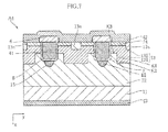
Fig. 1 is a fragmentary cross-sectional view of a semiconductor device according to a first embodiment of the present invention; -
Fig. 2 is a fragmentary cross-sectional view for explaining a manufacturing process of the semiconductor device shown inFig. 1 ; -
Fig. 3 is a fragmentary cross-sectional view for explaining a manufacturing process following the state shown inFig. 2 ; -
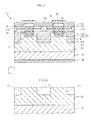
Fig. 4 is a fragmentary cross-sectional view of a semiconductor device according to a second embodiment of the present invention; -
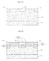
Fig. 5A is a fragmentary cross - sectional view for explaining a manufacturing process of the semiconductor device shown inFig. 4 ; -
Fig. 5B is a fragmentary cross-sectional view for explaining a manufacturing process following the state shown inFig. 5A ; -
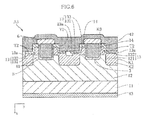
Fig. 6 is a fragmentary cross-sectional view of a semiconductor device according to a third embodiment of the present invention; -
Fig. 7 is a fragmentary cross-sectional view of a semiconductor device according to a fourth embodiment of the present invention; -
Fig. 8A is a fragmentary cross-sectional view for explaining a manufacturing process following the state shown inFig. 7 ; -
Fig. 8B is a fragmentary cross-sectional view for explaining a manufacturing process following the state shown inFig. 8A ; -
Fig. 9A is a fragmentary cross-sectional view for explaining a manufacturing process following the state shown inFig. 8B ; -
Fig. 9B is a fragmentary cross-sectional view for explaining a manufacturing process following the state shown inFig. 9A ; -
Fig. 10 is a fragmentary cross-sectional view for explaining a manufacturing process following the state shown inFig. 9B ; -
Fig, 11 is a fragmentary cross-sectional view of a semiconductor device according to a fifth embodiment of the present invention; and -
Fig. 12 is a fragmentary cross-sectional view of a conventional semiconductor device. - Hereunder, preferred embodiments of the present invention will be described in details, referring to the drawings.
-
Fig. 1 illustrates a semiconductor device according to a first embodiment of the present invention. The semiconductor device A1 according to this embodiment includes a first n-type semiconductor layer 11, a second n-type semiconductor layer 12, a p-type semiconductor layer 13, an n-type semiconductor region 14, a high - concentration p-type semiconductor region 13a, atrench 3, agate electrode 41, agate insulating layer 5, asource electrode 42, adrain electrode 43 and an interlayer dielectric 6. - The first n-
type semiconductor layer 11 is a substrate constituted of silicon carbide with a high-concentration impurity added thereto. The second n-type semiconductor layer 12 is provided on the first n-type semiconductor layer 11. The second n-type semiconductor layer 12 is constituted of silicon carbide with a low-concentration impurity added thereto. - The p-
type semiconductor layer 13 include a first p-type semiconductor layer 131 and a second p-type semiconductor layer 132. The first p-type semiconductor layer 131 is provided on the second n-type semiconductor laxer 12. Of the boundary between the first p-type semiconductor layer 131 and the second n-type semiconductor layer 12, a portion along a depthwise direction x of thetrench 3 will be referred to as a lateral boundary K1, and a portion along a widthwise direction y will be referred to as a bottom boundary K2. In this embodiment, the bottom boundary K2 is spaced from the boundary between the n-type semiconductor region 14 and thesource electrode 42, by approximately 1 µm. The impurity concentration of the first p-type semiconductor layer 131 is, for example, 1×1017cm-3 to 1×1020cm-3. The second p-type semiconductor layer 132 is provided on the first p-type semiconductor layer 131 and the second n-type semiconductor layer 12. Of the boundary between the second p-type semiconductor layer 132 and the second n-type semiconductor layer 12, a portion along the widthwise direction y will be referred to as a bottom boundary K3. The impurity concentration of the second p-type semiconductor layer 132 is, for example, 1×1016cm-3 to 1×1019cm-3. The n-type semiconductor region 14 is provided on the p-type semiconductor layer 13. The high-concentration p-type semiconductor region 13a is provided on the first p-type semiconductor layer 131. - The
trench 3 is formed so as to penetrate through the n-type semiconductor region 14 and the second p-type semiconductor layer 132, and to reach the second n-type semiconductor layer 12. Thetrench 3 and the first p-type semiconductor lawyer 131 are spaced from each other by approximately 0.3 µm, when viewed in the widthwise direction y. - Inside the
trench 3, thegate electrode 41 and thegate insulating layer 5 are located. Thegate electrode 41 is constituted of, for example, polysilicon. Alternatively, a metal such as aluminum may be employed to form thegate electrode 41. The gate insulating laxer 5 is constituted of silicon dioxide for example, and serves to insulate thegate electrode 41 from the second n-type semiconductor laxer 12, the p-type semiconductor layer 13, and the n-type semiconductor region 14. Thegate insulating layer 5 is provided along the inner wall of thetrench 3 and over the bottom portion and the lateral portion of thetrench 3. - In the depthwise direction x, the bottom boundary K3, the bottom portion of the
gate electrode 41, the bottom portion of thetrench 3, and the bottom boundary K2 are located in the mentioned order, downwardly inFig. 1 . - The
source electrode 42 is for example constituted of aluminum, and located in contact with the n-type semiconductor region 14 and the high-concentration p-type semiconductor region 13a. Thedrain electrode 43 is also constituted of aluminum for example, and located in contact with the first n-type semiconductor laxer 11. Thedrain electrode 43 is provided on the opposite side of the first n-type semiconductor layer 11 to the second n-type semiconductor layer 12. Theinterlayer dielectric 6 is formed so as to cover thegate electrode 41. - Now, an example of the manufacturing method of the semiconductor device A1 will be described, referring to
Figs. 2 and3 . - Referring first to
Fig. 2 , a semiconductor substrate which is to serve as the first n-type semiconductor layer 11 is prepared. On the upper surface of the substrate, the second n-type semiconductor layer 12 is formed through epitaxial crystal growth. Then a groove T1 is formed on the surface of the second n-type semiconductor layer 12. - Referring then to
Fig. 3 , the first p-type semiconductor layer 131 is formed inside the groove T1 through the epitaxial crystal growth. The surface of the substrate is then planarized. On the planarized substrate, the second p-type semiconductor layer 132 is formed through the epitaxial crystal growth. - Then a mask of a predetermined pattern is placed over the upper surface of the second p-
type semiconductor layer 132, and impurity ions (n-type or p-type) are injected. Thus the n-type semiconductor region 14 and the high-concentration p-type semiconductor region 13a are formed. - The above is followed by the formation of the
trench 3, thegate insulating layer 5 and thegate electrode 41 shown inFig. 1 . Then theinterlayer dielectric 6, thesource electrode 42, and thedrain electrode 43 are formed. Through the foregoing process, the semiconductor device A1 can be obtained. - The advantageous effects of the semiconductor device A1 will now be described hereunder. In this embodiment, the bottom boundary K2 is at a lower level than the bottom portion of the
trench 3, according to the orientation ofFig. 1 . Such configuration encourages the field concentration on the boundary between the first p-type semiconductor layer 131 and the second n-type semiconductor laxer 12. Accordingly, the field concentration on the bottom portion of thefrench 3 is mitigated. Mitigating the field concentration reduces the risk of dielectric breakdown in thegate insulating layer 5. As a result, the withstand voltage of the semiconductor device A1 can be improved. - The structure according to this embodiment allows reducing the impurity concentration of the second p-
type semiconductor layer 132. This facilitates lowering the threshold voltage of the semiconductor device A1. On the other hand, increasing the impurity concentration of the first p-type semiconductor layer 131 allows suppressing extension of a depletion layer in the first p-type semiconductor layer 131, thereby preventing a punch through phenomenon. -
Figs. 4 ,5A and 5B illustrate a second embodiment of the present invention. In these drawings, the constituents same as or similar to those of the foregoing embodiment are given the same numeral. The semiconductor device A2 according to this embodiment is different from the semiconductor device A1 according to the first embodiment in including a recessed portion T2. - In the semiconductor device A2 shown in
Fig. 4 , the impurity concentration in the first p-type semiconductor layer 131 is higher than that in the second p-type semiconductor layer 132, as in the first embodiment. - Above the first p-
type semiconductor layer 131 according to the orientation ofFig. 4 , a recessed portion T2 is provided. In this embodiment, the size of the opening of the recessed portion T2 in the widthwise direction y is slightly smaller than that of the first p-type semiconductor layer 131 in the widthwise direction y. The bottom portion of the recessed portion T2 is located higher than the bottom boundary K2, according toFig. 4 . Also, the bottom portion of the recessed portion T2 is located higher than the bottom boundary K3 inFig. 4 . The high-concentration p-type semiconductor region 13a is located below the recessed portion T2. It is not mandatory that the bottom portion of the recessed portion T2 is located higher than the bottom boundary K3. For example, the bottom portion of the recessed portion T2 may be located lower than the bottom portion of thefrench 3. The position of the bottom portion of the recessed portion T2 may be determined irrespective of the position of the bottom boundary K3 and the bottom portion of thetrench 3. - Referring now to
Figs. 5A and 5B , an example of the manufacturing method of the semiconductor device A2 will be described hereunder. - First, as shown in
Fig. 5A , a semiconductor substrate which is to serve as the first n-type semiconductor layer 11 is prepared. On the upper surface of the substrate, the second n-type semiconductor layer 12 is formed through the epitaxial crystal growth. Then the recessed portion T2 is formed on the surface of the second n-type semiconductor layer 12, in a depth of approximately 0.5 µm. - Referring then to
Fig. 5B , the first p-type semiconductor layer 131 is formed. To form the first p-type semiconductor layer 131, a mask (not shown) is placed over the upper surface of the substrate, and the recessed portion T2 is irradiated with impurity ions (p-type) from above infig. 5B , with energy of approximately 400 KeV. Then the region on the surface of the second n-type semiconductor layer 12 where the recessed portion T2 is not formed is irradiated with impurity ions (p-type), with generally the same energy. As a result, the second p-type semiconductor layer 132 is formed. Here, the ion concentration in the first p-type semiconductor layer 131 and the second p-type semiconductor layer 132 can be controlled by adjusting the duration of the ion irradiation. - Alternatively, the entire surface of the second n-
type semiconductor layer 12 may be irradiated with impurity ions from above inFig. 5B , without putting the mask on the upper surface of the substrate. By such impurity ion irradiation, the first p-type semiconductor layer 131 and the second p-type semiconductor layer 132 can be formed in different depths from the surface of the second n-type semiconductor layer 12. This process is especially useful in the case where it is not necessary to control the impurity concentration in the first p-type semiconductor layer 131 and the second p-type semiconductor layer 132. - The above is followed by the formation of the n-
type semiconductor region 14 and the high-concentration p-type semiconductor region 13a shown inFig. 4 . These regions can also be formed by injecting impurity ions (n-type or p-type) to the second n-type semiconductor layer 12. Then thetrench 3 is formed in the region where the second p-type semiconductor layer 132 has been formed. Inside thefrench 3, thegate insulating laxer 5 and thegate electrode 41 are formed. Then theinterlayer dielectric 6, thesource electrode 42, and thedrain electrode 43 are formed. Through the foregoing process, the semiconductor device A2 can be obtained. - According to this embodiment, providing the recessed portion T2 allows forming a deeper portion of the first p-
type semiconductor layer 131 by the ion irradiation with lower energy. -
Fig. 6 illustrates a third embodiment of the present invention. As in the preceding drawings, the constituents inFig. 6 same as or similar to those of the foregoing embodiments are given the same numeral. The semiconductor device A3 according to this embodiment is different from the semiconductor device A2 according to the second embodiment in that the n-type semiconductor region 14 is also provided under the recessed portion T2. Such configuration increases the contact area between thesource electrode 42 and the n-type semiconductor region 14. Accordingly, the contact resistance between thesource electrode 42 and the n-type semiconductor region 14 can be reduced, in the semiconductor device A3. -
Figs. 7 to 10 illustrate a fourth embodiment of the present invention. In these drawings, the constituents same as of similar to those of the foregoing embodiments are given the same numeral. The semiconductor device A4 according to this embodiment is different from the semiconductor device A1 according to the first embodiment in including a p-type semiconductor region 15. - As is apparent in
Fig. 7 , the p-type semiconductor region 15 is located in contact with the bottom portion of thetrench 3. The impurity concentration in the p-type semiconductor region 15 is, for example, 1×1016 cm-3 to 1×1021 cm-3. The size of the boundary between the p-type semiconductor region 15 and the bottom portion of thefrench 3 in the widthwise direction y is slightly smaller than that of thegate electrode 41 in the widthwise direction y. Also, a lowermost portion of the p-type semiconductor region 15 according to the orientation ofFig. 7 is located lower than the bottom boundary K2 in the depthwise direction x. Conversely, although not shown, the bottom boundary K2 may be located lower than the lowermost portion of the p-type semiconductor region 15. - Referring now to
Figs. 8 to 10 , an example of the manufacturing method of the semiconductor device A4 will be described hereunder. - The manufacturing method of the semiconductor device A4 is the same as that of the semiconductor device A1 according to the first embodiment, up to the state shown in
Fig. 3 . Accordingly, the description of the process up toFig. 3 is not repeated. Referring thus toFig. 8A , a plasma CVD is performed over the upper surface of the structure shown inFig. 3 , to thereby form asilicon dioxide layer 7. Thesilicon dioxide layer 7 serves as the mask for forming thetrench 3 and the p-type semiconductor region 15, as will be subsequently described. Proceeding toFig. 8B , a trench 3' is formed so as to penetrate through all of thesilicon dioxide layer 7, the n-type semiconductor region 14, and the p-type semiconductor layer 13. The trench 3' is to be formed into thetrench 3 shown inFig. 7 . Then the inner wall of the trench 3' is thermally oxidized (not shown). - Then as shown in
Fig. 9A , a polysilicon layer is formed all over the inner of the trench 3' and the upper surface of thesilicon dioxide layer 7. Then as shown inFigs. 9B and10 , a polysilicon layer ps1 and a polysilicon layer ps3 are removed, leaving a polysilicon layer ps2 unremoved. Impurity ions (p-type) are then injected to the bottom portion of the trench 3', as shown inFig. 10 . At this stage, the p-type semiconductor region 15 is formed. Then the entirety of thesilicon dioxide laxer 7 and the polysilicon layer ps2 are removed. This is followed by the same process as that described in the first embodiment. Thus, the semiconductor device A4 shown inFig. 7 can be obtained. - The advantageous effects of the semiconductor device A4 will now be described hereunder.
- The structure of the semiconductor device A4 allows further mitigating the field concentration on the bottom portion of the
french 3. Accordingly, the withstand voltage of the semiconductor device A4 can be further improved. Here, reducing the size of the p-type semiconductor region 15 in the widthwise direction y allows suppressing an increase in on-resistance. -
Fig, 11 illustrates a fifth embodiment of the present invention. InFig. 11 , the constituents same as or similar to those of the foregoing embodiments are given the same numeral. A difference between the semiconductor device A5 according to this embodiment and the semiconductor device A4 according to the fourth embodiment lies in the shape of thetrench 3. - As shown in
Fig. 11 , the additional p-type semiconductor layer 15 is provided so as to cover the bottom portion of thetrench 3. Such configuration allows further increasing the withstand voltage. Also, the bottom portion of thetrench 3 is formed in a trapezoidal shape. As a result, the additional p-type semiconductor layer 15 can be formed within an area overlapping with thefrench 3 in the widthwise direction y. The foregoing structure prevents the flow of electron in the semiconductor device A5 from being disturbed, thereby suppressing an increase in on-resistance. Consequently, the dielectric breakdown electric field can be further increased, while an increase in on-resistance can be suppressed. - The semiconductor device and the manufacturing method of the same according to the present invention are not limited to the foregoing embodiments. Specific structure and arrangement of the semiconductor device and the manufacturing method according to the present invention may be varied in different manners.
Claims (8)
- A semiconductor device comprising:a semiconductor layer having a first face provided witch a trench and a second face opposite to the first face;a gate electrode provided in the trench; andan insulating layer provided in the trench so as to insulate the semiconductor layer and the gate electrode from each other;wherein the semiconductor layer includes a first semiconductor layer of a first conductivity type, and a second semiconductor layer of a second conductivity type opposite to the first conductivity type,wherein the trench is formed so as to penetrate through the second semiconductor layer and to reach the first semiconductor layer,wherein the second semiconductor layer includes a close portion closer to the second face of the semiconductor layer than the trench is.
- The semiconductor device according to claim 1, wherein the second semiconductor layer includes a channel region formed the trench and in contact with the first semiconductor layer, and
wherein impurity concentration in the channel region is lower than impurity concentration in the close portion, - The semiconductor device according to claim 1, the semiconductor layer further includes a semiconductor region formed around the trench,
wherein a recessed portion is provided at the first semiconductor layer, the second semiconductor layer, or the semiconductor region, and
wherein the close portion and the recessed portion are so as to overlap in a widthwise direction perpendicular to a depthwise direction of the trench. - The semiconductor device according to claim 1, wherein the semiconductor layer further includes an additional semiconductor region of the second conductivity type, and
the additional semiconductor region is formed in the first semiconductor layer and spaced from the second semiconductor layer. - The semiconductor device according to claim 4, wherein the additional semiconductor region is in contact with a bottom portion of the trench.
- The semiconductor device according to claim 4, wherein the additional semiconductor region is formed so as to make contact with the bottom portion of the trench and a lateral portion of the trench.
- The semiconductor device according to claim 4, wherein the additional semiconductor region is in contact the trench, and
wherein a boundary between the additional semiconductor region the trench is located only inside an opening of the trench, in a depthwise view of the trench. - A method of manufacturing a semiconductor device, the method comprising:forming a trench and a recessed portion on a surface of a semiconductor substrate;forming an insulating layer in the trench;forming a gate electrode stacked on the insulating layer in the trench;irradiating the recessed portion with ions thereby forming a first semiconductor region of a conductivity type different from a conductivity type of the semiconductor substrate, the first semiconductor region being located close to a bottom portion of the recessed portion; andirradiating the surface of the semiconductor substrate with ions thereby forming a second semiconductor region of a conductivity type different from the conductivity type of the semiconductor substrate;wherein the first and the second semiconductor regions are connected with each other, andwherein the trench penetrates through the second semiconductor region.
Priority Applications (5)
| Application Number | Priority Date | Filing Date | Title |
|---|---|---|---|
| EP20152069.9A EP3660925A1 (en) | 2008-03-26 | 2009-03-26 | Semiconductor device, and method for manufacturing the same |
| EP15181700.4A EP2966690B1 (en) | 2008-03-26 | 2009-03-26 | Semiconductor device and method for manufacturing the same |
| EP23207308.0A EP4297097A3 (en) | 2008-03-26 | 2009-03-26 | Semiconductor device, and method for manufacturing the same |
| EP24169273.0A EP4372824A3 (en) | 2008-03-26 | 2009-03-26 | Semiconductor device, and method for manufacturing the same |
| EP22179241.9A EP4095928B1 (en) | 2008-03-26 | 2009-03-26 | Semiconductor device |
Applications Claiming Priority (3)
| Application Number | Priority Date | Filing Date | Title |
|---|---|---|---|
| JP2008080216 | 2008-03-26 | ||
| JP2008333530A JP5721308B2 (en) | 2008-03-26 | 2008-12-26 | Semiconductor device |
| PCT/JP2009/056109 WO2009119735A1 (en) | 2008-03-26 | 2009-03-26 | Semiconductor device, and method for manufacturing the same |
Related Child Applications (5)
| Application Number | Title | Priority Date | Filing Date |
|---|---|---|---|
| EP15181700.4A Division EP2966690B1 (en) | 2008-03-26 | 2009-03-26 | Semiconductor device and method for manufacturing the same |
| EP24169273.0A Division EP4372824A3 (en) | 2008-03-26 | 2009-03-26 | Semiconductor device, and method for manufacturing the same |
| EP23207308.0A Division EP4297097A3 (en) | 2008-03-26 | 2009-03-26 | Semiconductor device, and method for manufacturing the same |
| EP20152069.9A Division EP3660925A1 (en) | 2008-03-26 | 2009-03-26 | Semiconductor device, and method for manufacturing the same |
| EP22179241.9A Division EP4095928B1 (en) | 2008-03-26 | 2009-03-26 | Semiconductor device |
Publications (2)
| Publication Number | Publication Date |
|---|---|
| EP2276066A1 true EP2276066A1 (en) | 2011-01-19 |
| EP2276066A4 EP2276066A4 (en) | 2011-11-16 |
Family
ID=41113923
Family Applications (6)
| Application Number | Title | Priority Date | Filing Date |
|---|---|---|---|
| EP22179241.9A Active EP4095928B1 (en) | 2008-03-26 | 2009-03-26 | Semiconductor device |
| EP23207308.0A Pending EP4297097A3 (en) | 2008-03-26 | 2009-03-26 | Semiconductor device, and method for manufacturing the same |
| EP15181700.4A Active EP2966690B1 (en) | 2008-03-26 | 2009-03-26 | Semiconductor device and method for manufacturing the same |
| EP09724334A Ceased EP2276066A4 (en) | 2008-03-26 | 2009-03-26 | SEMICONDUCTOR DEVICE AND METHOD FOR MANUFACTURING THE SAME |
| EP20152069.9A Pending EP3660925A1 (en) | 2008-03-26 | 2009-03-26 | Semiconductor device, and method for manufacturing the same |
| EP24169273.0A Pending EP4372824A3 (en) | 2008-03-26 | 2009-03-26 | Semiconductor device, and method for manufacturing the same |
Family Applications Before (3)
| Application Number | Title | Priority Date | Filing Date |
|---|---|---|---|
| EP22179241.9A Active EP4095928B1 (en) | 2008-03-26 | 2009-03-26 | Semiconductor device |
| EP23207308.0A Pending EP4297097A3 (en) | 2008-03-26 | 2009-03-26 | Semiconductor device, and method for manufacturing the same |
| EP15181700.4A Active EP2966690B1 (en) | 2008-03-26 | 2009-03-26 | Semiconductor device and method for manufacturing the same |
Family Applications After (2)
| Application Number | Title | Priority Date | Filing Date |
|---|---|---|---|
| EP20152069.9A Pending EP3660925A1 (en) | 2008-03-26 | 2009-03-26 | Semiconductor device, and method for manufacturing the same |
| EP24169273.0A Pending EP4372824A3 (en) | 2008-03-26 | 2009-03-26 | Semiconductor device, and method for manufacturing the same |
Country Status (6)
| Country | Link |
|---|---|
| US (10) | US8283721B2 (en) |
| EP (6) | EP4095928B1 (en) |
| JP (1) | JP5721308B2 (en) |
| CN (1) | CN101981701B (en) |
| DE (1) | DE202009019196U1 (en) |
| WO (1) | WO2009119735A1 (en) |
Cited By (6)
| Publication number | Priority date | Publication date | Assignee | Title |
|---|---|---|---|---|
| WO2014115494A1 (en) * | 2013-01-25 | 2014-07-31 | Kabushiki Kaisha Toyota Chuo Kenkyusho | Method of manufacturing semiconductor device |
| WO2015104084A1 (en) * | 2014-01-13 | 2015-07-16 | Robert Bosch Gmbh | Trench mosfet transistor device and corresponding production method |
| IT201800007780A1 (en) * | 2018-08-02 | 2020-02-02 | St Microelectronics Srl | SILICON CARBIDE MOSFET DEVICE AND ITS MANUFACTURING METHOD |
| EP3712959A4 (en) * | 2017-11-15 | 2021-07-28 | Flosfia Inc. | SEMICONDUCTOR DEVICE |
| EP3930006A1 (en) * | 2020-06-24 | 2021-12-29 | Infineon Technologies AG | Semiconductor device including trench gate structure and buried shielding region and method of manufacturing |
| US12581700B2 (en) | 2011-02-02 | 2026-03-17 | Rohm Co., Ltd. | Semiconductor device |
Families Citing this family (71)
| Publication number | Priority date | Publication date | Assignee | Title |
|---|---|---|---|---|
| JP5721308B2 (en) | 2008-03-26 | 2015-05-20 | ローム株式会社 | Semiconductor device |
| JP5613995B2 (en) * | 2009-04-28 | 2014-10-29 | 富士電機株式会社 | Silicon carbide semiconductor device and manufacturing method thereof |
| JP5463725B2 (en) * | 2009-04-28 | 2014-04-09 | 富士電機株式会社 | Silicon carbide semiconductor device and manufacturing method thereof |
| JP5680326B2 (en) * | 2010-04-01 | 2015-03-04 | トヨタ自動車株式会社 | Manufacturing method of semiconductor device |
| US8525254B2 (en) * | 2010-08-12 | 2013-09-03 | Infineon Technologies Austria Ag | Silicone carbide trench semiconductor device |
| JP2012069824A (en) * | 2010-09-24 | 2012-04-05 | Seiko Instruments Inc | Semiconductor device and manufacturing method therefor |
| JP5858933B2 (en) * | 2011-02-02 | 2016-02-10 | ローム株式会社 | Semiconductor device |
| JP2014099670A (en) * | 2011-02-02 | 2014-05-29 | Rohm Co Ltd | Semiconductor apparatus and manufacturing method thereof |
| JP5750948B2 (en) * | 2011-03-11 | 2015-07-22 | 三菱電機株式会社 | Silicon carbide semiconductor device and manufacturing method thereof |
| JP6270799B2 (en) * | 2011-05-16 | 2018-01-31 | ルネサスエレクトロニクス株式会社 | Semiconductor device |
| JP5920970B2 (en) | 2011-11-30 | 2016-05-24 | ローム株式会社 | Semiconductor device |
| CN103035680B (en) * | 2012-05-08 | 2015-10-14 | 上海华虹宏力半导体制造有限公司 | Super-junction device |
| EP2860761A4 (en) | 2012-05-31 | 2016-02-24 | Nat Inst Of Advanced Ind Scien | SEMICONDUCTOR DEVICE |
| JP6065303B2 (en) | 2012-06-15 | 2017-01-25 | ローム株式会社 | Switching device |
| JP5985662B2 (en) | 2013-01-23 | 2016-09-06 | 株式会社日立製作所 | Silicon carbide semiconductor device and manufacturing method thereof |
| JP6107597B2 (en) * | 2013-03-26 | 2017-04-05 | 豊田合成株式会社 | Semiconductor device and manufacturing method thereof |
| JP6077380B2 (en) * | 2013-04-24 | 2017-02-08 | トヨタ自動車株式会社 | Semiconductor device |
| DE102013209256A1 (en) | 2013-05-17 | 2014-11-20 | Robert Bosch Gmbh | Metal Oxide Semiconductor Field Effect Transistor and Method of Making a Metal Oxide Semiconductor Field Effect Transistor |
| JP6098417B2 (en) | 2013-07-26 | 2017-03-22 | 住友電気工業株式会社 | Silicon carbide semiconductor device and manufacturing method thereof |
| JP6135364B2 (en) * | 2013-07-26 | 2017-05-31 | 住友電気工業株式会社 | Silicon carbide semiconductor device and manufacturing method thereof |
| JP6207627B2 (en) * | 2013-11-13 | 2017-10-04 | 三菱電機株式会社 | Semiconductor device |
| JP6341074B2 (en) * | 2014-01-24 | 2018-06-13 | 株式会社デンソー | Manufacturing method of semiconductor device |
| JP6179409B2 (en) * | 2014-01-24 | 2017-08-16 | 株式会社デンソー | Method for manufacturing silicon carbide semiconductor device |
| JP6428489B2 (en) | 2014-09-16 | 2018-11-28 | 株式会社デンソー | Silicon carbide semiconductor device and manufacturing method thereof |
| JP6064977B2 (en) * | 2014-11-06 | 2017-01-25 | 三菱電機株式会社 | Silicon carbide semiconductor device |
| WO2016116998A1 (en) * | 2015-01-19 | 2016-07-28 | 株式会社日立製作所 | Semiconductor device, method for manufacturing same, power conversion device, three-phase motor system, automobile, and railway carriage |
| WO2016129068A1 (en) | 2015-02-12 | 2016-08-18 | 株式会社日立製作所 | Semiconductor device and method for manufacturing same, power conversion device, three-phase motor system, automobile, and railway carriage |
| JP6526981B2 (en) | 2015-02-13 | 2019-06-05 | ローム株式会社 | Semiconductor device and semiconductor module |
| JP6485299B2 (en) * | 2015-06-05 | 2019-03-20 | 豊田合成株式会社 | Semiconductor device, method for manufacturing the same, and power conversion device |
| JP6584857B2 (en) | 2015-08-11 | 2019-10-02 | 株式会社東芝 | Semiconductor device |
| JP6478884B2 (en) * | 2015-09-11 | 2019-03-06 | 株式会社東芝 | Semiconductor device |
| CN108028282B (en) | 2015-10-16 | 2021-06-15 | 富士电机株式会社 | Semiconductor device and method for manufacturing semiconductor device |
| CN108352402B (en) | 2015-10-16 | 2020-12-18 | 富士电机株式会社 | Semiconductor device and manufacturing method of semiconductor device |
| JP6759563B2 (en) | 2015-11-16 | 2020-09-23 | 富士電機株式会社 | Semiconductor devices and methods for manufacturing semiconductor devices |
| KR20180081596A (en) | 2015-11-16 | 2018-07-16 | 아락세스 파마 엘엘씨 | Substituted quinazoline compounds comprising substituted heterocyclic groups and methods for their use |
| JP6232089B2 (en) * | 2016-02-24 | 2017-11-15 | ローム株式会社 | Semiconductor device |
| JP6658257B2 (en) * | 2016-04-22 | 2020-03-04 | 住友電気工業株式会社 | Silicon carbide semiconductor device |
| JP6926261B2 (en) * | 2016-07-06 | 2021-08-25 | 株式会社東芝 | Semiconductor devices and their manufacturing methods |
| JP2018006639A (en) | 2016-07-06 | 2018-01-11 | 株式会社東芝 | Semiconductor and manufacturing method therefor |
| JP6625938B2 (en) | 2016-07-22 | 2019-12-25 | 株式会社東芝 | Semiconductor device, method of manufacturing semiconductor device, inverter circuit, drive device, vehicle, and elevator |
| JP6919159B2 (en) * | 2016-07-29 | 2021-08-18 | 富士電機株式会社 | Silicon Carbide Semiconductor Device and Method for Manufacturing Silicon Carbide Semiconductor Device |
| JP6855700B2 (en) * | 2016-08-05 | 2021-04-07 | 富士電機株式会社 | Semiconductor devices and their manufacturing methods |
| JP6766512B2 (en) * | 2016-08-05 | 2020-10-14 | 富士電機株式会社 | Semiconductor devices and methods for manufacturing semiconductor devices |
| GB201615007D0 (en) * | 2016-09-05 | 2016-10-19 | Jaguar Land Rover Ltd | A lamp assembly for an automobile, a headlamp comprising such a lamp assembly, and an automobile comprising such a lamp assembly |
| JP6848317B2 (en) * | 2016-10-05 | 2021-03-24 | 富士電機株式会社 | Semiconductor devices and methods for manufacturing semiconductor devices |
| JP6848382B2 (en) | 2016-11-16 | 2021-03-24 | 富士電機株式会社 | Semiconductor devices and methods for manufacturing semiconductor devices |
| JP6918302B2 (en) | 2016-12-20 | 2021-08-11 | 富士電機株式会社 | Silicon Carbide Semiconductor Device and Method for Manufacturing Silicon Carbide Semiconductor Device |
| JP6853977B2 (en) | 2017-01-16 | 2021-04-07 | 国立研究開発法人産業技術総合研究所 | Semiconductor devices and methods for manufacturing semiconductor devices |
| CN109564943B (en) * | 2017-02-13 | 2022-06-24 | 富士电机株式会社 | Semiconductor device with a plurality of semiconductor chips |
| JP6972680B2 (en) | 2017-06-09 | 2021-11-24 | 富士電機株式会社 | Silicon Carbide Semiconductor Device and Method for Manufacturing Silicon Carbide Semiconductor Device |
| JP6950290B2 (en) | 2017-06-09 | 2021-10-13 | 富士電機株式会社 | Semiconductor devices and manufacturing methods for semiconductor devices |
| JP7029710B2 (en) | 2017-06-16 | 2022-03-04 | 富士電機株式会社 | Semiconductor device |
| JP7007053B2 (en) * | 2017-10-17 | 2022-01-24 | 株式会社ディスコ | Lift-off method |
| JP6960119B2 (en) * | 2017-11-28 | 2021-11-05 | 株式会社東芝 | Semiconductor device |
| JP7057555B2 (en) * | 2017-11-29 | 2022-04-20 | 国立研究開発法人産業技術総合研究所 | Semiconductor device |
| JP2018085531A (en) * | 2018-01-05 | 2018-05-31 | ローム株式会社 | Semiconductor device |
| JP6998244B2 (en) | 2018-03-14 | 2022-01-18 | ルネサスエレクトロニクス株式会社 | Manufacturing method of semiconductor device |
| JP2018129558A (en) * | 2018-05-24 | 2018-08-16 | ローム株式会社 | Semiconductor device |
| JP7002998B2 (en) | 2018-05-28 | 2022-01-20 | 株式会社日立製作所 | Semiconductor devices and their manufacturing methods, power conversion devices, three-phase motor systems, automobiles, and railroad vehicles |
| JP7075876B2 (en) | 2018-12-25 | 2022-05-26 | 株式会社日立製作所 | Silicon Carbide Semiconductor Equipment, Power Conversion Equipment, 3-Phase Motor Systems, Automobiles and Rail Vehicles |
| JP6808766B2 (en) * | 2019-01-11 | 2021-01-06 | 株式会社東芝 | Semiconductor device |
| JP2020129675A (en) * | 2020-04-21 | 2020-08-27 | ローム株式会社 | Semiconductor device |
| TWI752512B (en) * | 2020-05-29 | 2022-01-11 | 國立陽明交通大學 | Trench transistor and manufacturing method thereof |
| US20240282810A1 (en) * | 2022-01-04 | 2024-08-22 | Hubei Jiufengshan Laboratory | Silicon carbide mosfet device and manufacturing method therefore |
| CN114496785B (en) * | 2022-04-18 | 2022-08-02 | 深圳芯能半导体技术有限公司 | A T-type bottom-protected trench-type silicon carbide MOSFET and preparation method thereof |
| CN114496784B (en) * | 2022-04-18 | 2022-07-12 | 深圳芯能半导体技术有限公司 | Bottom protection ground trench type silicon carbide MOSFET and preparation method thereof |
| CN114496783B (en) * | 2022-04-18 | 2022-08-05 | 深圳芯能半导体技术有限公司 | Groove type silicon carbide MOSFET prepared based on buffer layer and preparation method thereof |
| CN116469923B (en) * | 2023-04-25 | 2023-10-20 | 南京第三代半导体技术创新中心有限公司 | High-reliability trench silicon carbide MOSFET device and manufacturing method thereof |
| CN116344587A (en) * | 2023-04-26 | 2023-06-27 | 无锡新洁能股份有限公司 | A trench silicon carbide MOSFET device and its manufacturing process |
| KR20250058278A (en) * | 2023-10-23 | 2025-04-30 | 주식회사 엘엑스세미콘 | Power semiconductor device, power converter including the same and A method for manufacturing a semiconductor device |
| TWI902462B (en) * | 2024-09-23 | 2025-10-21 | 漢磊科技股份有限公司 | Semiconductor device and method for manufacturing the same |
Family Cites Families (34)
| Publication number | Priority date | Publication date | Assignee | Title |
|---|---|---|---|---|
| US4587712A (en) * | 1981-11-23 | 1986-05-13 | General Electric Company | Method for making vertical channel field controlled device employing a recessed gate structure |
| US4945394A (en) * | 1987-10-26 | 1990-07-31 | North Carolina State University | Bipolar junction transistor on silicon carbide |
| JP2647884B2 (en) | 1988-01-27 | 1997-08-27 | 株式会社日立製作所 | Method for manufacturing semiconductor device |
| IT1218200B (en) * | 1988-03-29 | 1990-04-12 | Sgs Thomson Microelectronics | MANUFACTURING PROCEDURE OF A MOS SEMICONDUCTIVE POWER DEVICE WITH CONDUCTIVITY MODULATION (HIMOS) AND DEVICES OBTAINED WITH IT |
| US5168331A (en) * | 1991-01-31 | 1992-12-01 | Siliconix Incorporated | Power metal-oxide-semiconductor field effect transistor |
| JPH0582792A (en) * | 1991-09-25 | 1993-04-02 | Toshiba Corp | Manufacture of semiconductor device |
| US5910669A (en) * | 1992-07-24 | 1999-06-08 | Siliconix Incorporated | Field effect Trench transistor having lightly doped epitaxial region on the surface portion thereof |
| US5341011A (en) * | 1993-03-15 | 1994-08-23 | Siliconix Incorporated | Short channel trenched DMOS transistor |
| US5689128A (en) * | 1995-08-21 | 1997-11-18 | Siliconix Incorporated | High density trenched DMOS transistor |
| US5719409A (en) | 1996-06-06 | 1998-02-17 | Cree Research, Inc. | Silicon carbide metal-insulator semiconductor field effect transistor |
| JPH1098188A (en) * | 1996-08-01 | 1998-04-14 | Kansai Electric Power Co Inc:The | Insulated gate semiconductor device |
| JPH10321848A (en) * | 1997-05-22 | 1998-12-04 | Nissan Motor Co Ltd | Method for manufacturing semiconductor device |
| US6110799A (en) | 1997-06-30 | 2000-08-29 | Intersil Corporation | Trench contact process |
| US5763914A (en) * | 1997-07-16 | 1998-06-09 | Megamos Corporation | Cell topology for power transistors with increased packing density |
| US6342709B1 (en) | 1997-12-10 | 2002-01-29 | The Kansai Electric Power Co., Inc. | Insulated gate semiconductor device |
| GB9826291D0 (en) * | 1998-12-02 | 1999-01-20 | Koninkl Philips Electronics Nv | Field-effect semi-conductor devices |
| JP4738562B2 (en) * | 2000-03-15 | 2011-08-03 | 三菱電機株式会社 | Manufacturing method of semiconductor device |
| US6353046B1 (en) | 2000-04-28 | 2002-03-05 | General Electric Company | Fire-retarded polycarbonate resin composition |
| JP2002043570A (en) * | 2000-07-26 | 2002-02-08 | Sanyo Electric Co Ltd | Method for manufacturing semiconductor device |
| JP3652322B2 (en) * | 2002-04-30 | 2005-05-25 | Necエレクトロニクス株式会社 | Vertical MOSFET and manufacturing method thereof |
| JP3979258B2 (en) * | 2002-05-21 | 2007-09-19 | 富士電機デバイステクノロジー株式会社 | MIS semiconductor device and manufacturing method thereof |
| US6919599B2 (en) * | 2002-06-28 | 2005-07-19 | International Rectifier Corporation | Short channel trench MOSFET with reduced gate charge |
| JP4099029B2 (en) * | 2002-10-16 | 2008-06-11 | 株式会社豊田中央研究所 | Trench gate type semiconductor device |
| US7638841B2 (en) * | 2003-05-20 | 2009-12-29 | Fairchild Semiconductor Corporation | Power semiconductor devices and methods of manufacture |
| US7368777B2 (en) * | 2003-12-30 | 2008-05-06 | Fairchild Semiconductor Corporation | Accumulation device with charge balance structure and method of forming the same |
| JP2006093430A (en) | 2004-09-24 | 2006-04-06 | Nec Electronics Corp | Semiconductor device |
| AT504998A2 (en) * | 2005-04-06 | 2008-09-15 | Fairchild Semiconductor | TRENCHED-GATE FIELD EFFECT TRANSISTORS AND METHOD FOR MAKING THE SAME |
| JP2007027193A (en) * | 2005-07-12 | 2007-02-01 | Renesas Technology Corp | Semiconductor device, method for manufacturing the same, and non-insulated DC / DC converter |
| US7851349B2 (en) * | 2005-09-26 | 2010-12-14 | Infineon Technologies Austria Ag | Method for producing a connection electrode for two semiconductor zones arranged one above another |
| JP2007221024A (en) * | 2006-02-20 | 2007-08-30 | Toshiba Corp | Semiconductor device |
| CN101467258B (en) * | 2006-04-21 | 2012-02-08 | 意法半导体股份有限公司 | Process for manufacturing a power semiconductor device and corresponding power semiconductor device |
| JP4450241B2 (en) * | 2007-03-20 | 2010-04-14 | 株式会社デンソー | Method for manufacturing silicon carbide semiconductor device |
| JP5721308B2 (en) * | 2008-03-26 | 2015-05-20 | ローム株式会社 | Semiconductor device |
| JP2010050161A (en) * | 2008-08-19 | 2010-03-04 | Nec Electronics Corp | Semiconductor device |
-
2008
- 2008-12-26 JP JP2008333530A patent/JP5721308B2/en active Active
-
2009
- 2009-03-26 EP EP22179241.9A patent/EP4095928B1/en active Active
- 2009-03-26 EP EP23207308.0A patent/EP4297097A3/en active Pending
- 2009-03-26 EP EP15181700.4A patent/EP2966690B1/en active Active
- 2009-03-26 DE DE202009019196.6U patent/DE202009019196U1/en not_active Expired - Lifetime
- 2009-03-26 US US12/934,012 patent/US8283721B2/en active Active
- 2009-03-26 CN CN2009801104895A patent/CN101981701B/en active Active
- 2009-03-26 WO PCT/JP2009/056109 patent/WO2009119735A1/en not_active Ceased
- 2009-03-26 EP EP09724334A patent/EP2276066A4/en not_active Ceased
- 2009-03-26 EP EP20152069.9A patent/EP3660925A1/en active Pending
- 2009-03-26 EP EP24169273.0A patent/EP4372824A3/en active Pending
-
2012
- 2012-09-13 US US13/614,510 patent/US9166038B2/en active Active
-
2015
- 2015-09-15 US US14/854,752 patent/US9496387B2/en active Active
-
2016
- 2016-10-24 US US15/332,624 patent/US10290733B2/en active Active
-
2019
- 2019-04-09 US US16/379,038 patent/US10686067B2/en active Active
-
2020
- 2020-05-13 US US15/930,784 patent/US11127851B2/en active Active
-
2021
- 2021-08-24 US US17/410,661 patent/US12034073B2/en active Active
-
2023
- 2023-09-14 US US18/466,875 patent/US12009420B2/en active Active
-
2024
- 2024-02-29 US US18/590,999 patent/US20240204097A1/en active Pending
-
2025
- 2025-10-28 US US19/370,796 patent/US20260052729A1/en active Pending
Cited By (11)
| Publication number | Priority date | Publication date | Assignee | Title |
|---|---|---|---|---|
| US12581700B2 (en) | 2011-02-02 | 2026-03-17 | Rohm Co., Ltd. | Semiconductor device |
| WO2014115494A1 (en) * | 2013-01-25 | 2014-07-31 | Kabushiki Kaisha Toyota Chuo Kenkyusho | Method of manufacturing semiconductor device |
| KR20150074185A (en) * | 2013-01-25 | 2015-07-01 | 도요타 지도샤(주) | Method of manufacturing semiconductor device |
| US9660046B2 (en) | 2013-01-25 | 2017-05-23 | Kabushiki Kaisha Toyota Chuo Kenkyusho | Method of manufacturing semiconductor device |
| WO2015104084A1 (en) * | 2014-01-13 | 2015-07-16 | Robert Bosch Gmbh | Trench mosfet transistor device and corresponding production method |
| EP3712959A4 (en) * | 2017-11-15 | 2021-07-28 | Flosfia Inc. | SEMICONDUCTOR DEVICE |
| US11594601B2 (en) | 2017-11-15 | 2023-02-28 | Flosfia Inc. | Semiconductor apparatus |
| IT201800007780A1 (en) * | 2018-08-02 | 2020-02-02 | St Microelectronics Srl | SILICON CARBIDE MOSFET DEVICE AND ITS MANUFACTURING METHOD |
| EP3605615A1 (en) * | 2018-08-02 | 2020-02-05 | STMicroelectronics S.r.l. | Silicon carbide mosfet device and manufacturing method thereof |
| EP3930006A1 (en) * | 2020-06-24 | 2021-12-29 | Infineon Technologies AG | Semiconductor device including trench gate structure and buried shielding region and method of manufacturing |
| US11961904B2 (en) | 2020-06-24 | 2024-04-16 | Infineon Technologies Ag | Semiconductor device including trench gate structure and buried shielding region and method of manufacturing |
Also Published As
Similar Documents
| Publication | Publication Date | Title |
|---|---|---|
| US20240204097A1 (en) | Semiconductor device, and method for manufacturing the same | |
| US8466025B2 (en) | Semiconductor device structures and related processes | |
| JP5767857B2 (en) | Trench-type MOSFET and manufacturing method thereof | |
| EP2293336A1 (en) | Semiconductor device | |
| JP2010278312A (en) | Semiconductor device | |
| JP5807597B2 (en) | Semiconductor device and manufacturing method of semiconductor device | |
| US20060160310A1 (en) | Semiconductor device and method for fabricating the same | |
| JP2010056432A (en) | Insulated-gate semiconductor device and method of manufacturing the same | |
| JP2010245256A (en) | Semiconductor device and manufacturing method thereof | |
| JP2005236142A (en) | Horizontal short-channel DMOS, method for manufacturing the same, and semiconductor device | |
| JP2012049573A (en) | Semiconductor device, and method of manufacturing the same |
Legal Events
| Date | Code | Title | Description |
|---|---|---|---|
| PUAI | Public reference made under article 153(3) epc to a published international application that has entered the european phase |
Free format text: ORIGINAL CODE: 0009012 |
|
| 17P | Request for examination filed |
Effective date: 20101022 |
|
| AK | Designated contracting states |
Kind code of ref document: A1 Designated state(s): AT BE BG CH CY CZ DE DK EE ES FI FR GB GR HR HU IE IS IT LI LT LU LV MC MK MT NL NO PL PT RO SE SI SK TR |
|
| AX | Request for extension of the european patent |
Extension state: AL BA RS |
|
| DAX | Request for extension of the european patent (deleted) | ||
| A4 | Supplementary search report drawn up and despatched |
Effective date: 20111014 |
|
| RIC1 | Information provided on ipc code assigned before grant |
Ipc: H01L 29/12 20060101ALI20111010BHEP Ipc: H01L 21/336 20060101ALI20111010BHEP Ipc: H01L 29/78 20060101AFI20111010BHEP |
|
| 17Q | First examination report despatched |
Effective date: 20130802 |
|
| REG | Reference to a national code |
Ref country code: DE Ref legal event code: R003 |
|
| STAA | Information on the status of an ep patent application or granted ep patent |
Free format text: STATUS: THE APPLICATION HAS BEEN REFUSED |
|
| 18R | Application refused |
Effective date: 20150424 |