EP2237101A1 - Flüssigkristallmodul - Google Patents
Flüssigkristallmodul Download PDFInfo
- Publication number
- EP2237101A1 EP2237101A1 EP10158556A EP10158556A EP2237101A1 EP 2237101 A1 EP2237101 A1 EP 2237101A1 EP 10158556 A EP10158556 A EP 10158556A EP 10158556 A EP10158556 A EP 10158556A EP 2237101 A1 EP2237101 A1 EP 2237101A1
- Authority
- EP
- European Patent Office
- Prior art keywords
- terminals
- liquid crystal
- lead
- terminal
- row
- Prior art date
- Legal status (The legal status is an assumption and is not a legal conclusion. Google has not performed a legal analysis and makes no representation as to the accuracy of the status listed.)
- Ceased
Links
- 239000004973 liquid crystal related substance Substances 0.000 title claims abstract description 71
- 210000002858 crystal cell Anatomy 0.000 claims abstract description 42
- 230000006835 compression Effects 0.000 claims abstract description 32
- 238000007906 compression Methods 0.000 claims abstract description 32
- 238000000034 method Methods 0.000 description 32
- 239000011295 pitch Substances 0.000 description 21
- 230000000007 visual effect Effects 0.000 description 5
- 239000011521 glass Substances 0.000 description 4
- 239000000758 substrate Substances 0.000 description 4
- 230000002411 adverse Effects 0.000 description 2
- 210000004027 cell Anatomy 0.000 description 2
- 230000012447 hatching Effects 0.000 description 2
- 239000007788 liquid Substances 0.000 description 2
- 238000012986 modification Methods 0.000 description 2
- 230000004048 modification Effects 0.000 description 2
- 229920001721 polyimide Polymers 0.000 description 1
- 239000009719 polyimide resin Substances 0.000 description 1
- 239000011347 resin Substances 0.000 description 1
- 229920005989 resin Polymers 0.000 description 1
Images



Classifications
-
- H—ELECTRICITY
- H05—ELECTRIC TECHNIQUES NOT OTHERWISE PROVIDED FOR
- H05K—PRINTED CIRCUITS; CASINGS OR CONSTRUCTIONAL DETAILS OF ELECTRIC APPARATUS; MANUFACTURE OF ASSEMBLAGES OF ELECTRICAL COMPONENTS
- H05K3/00—Apparatus or processes for manufacturing printed circuits
- H05K3/36—Assembling printed circuits with other printed circuits
- H05K3/361—Assembling flexible printed circuits with other printed circuits
-
- G—PHYSICS
- G02—OPTICS
- G02F—OPTICAL DEVICES OR ARRANGEMENTS FOR THE CONTROL OF LIGHT BY MODIFICATION OF THE OPTICAL PROPERTIES OF THE MEDIA OF THE ELEMENTS INVOLVED THEREIN; NON-LINEAR OPTICS; FREQUENCY-CHANGING OF LIGHT; OPTICAL LOGIC ELEMENTS; OPTICAL ANALOGUE/DIGITAL CONVERTERS
- G02F1/00—Devices or arrangements for the control of the intensity, colour, phase, polarisation or direction of light arriving from an independent light source, e.g. switching, gating or modulating; Non-linear optics
- G02F1/01—Devices or arrangements for the control of the intensity, colour, phase, polarisation or direction of light arriving from an independent light source, e.g. switching, gating or modulating; Non-linear optics for the control of the intensity, phase, polarisation or colour
- G02F1/13—Devices or arrangements for the control of the intensity, colour, phase, polarisation or direction of light arriving from an independent light source, e.g. switching, gating or modulating; Non-linear optics for the control of the intensity, phase, polarisation or colour based on liquid crystals, e.g. single liquid crystal display cells
- G02F1/133—Constructional arrangements; Operation of liquid crystal cells; Circuit arrangements
- G02F1/1333—Constructional arrangements; Manufacturing methods
- G02F1/1345—Conductors connecting electrodes to cell terminals
- G02F1/13452—Conductors connecting driver circuitry and terminals of panels
-
- H—ELECTRICITY
- H05—ELECTRIC TECHNIQUES NOT OTHERWISE PROVIDED FOR
- H05K—PRINTED CIRCUITS; CASINGS OR CONSTRUCTIONAL DETAILS OF ELECTRIC APPARATUS; MANUFACTURE OF ASSEMBLAGES OF ELECTRICAL COMPONENTS
- H05K1/00—Printed circuits
- H05K1/02—Details
- H05K1/0266—Marks, test patterns or identification means
- H05K1/0269—Marks, test patterns or identification means for visual or optical inspection
-
- H—ELECTRICITY
- H05—ELECTRIC TECHNIQUES NOT OTHERWISE PROVIDED FOR
- H05K—PRINTED CIRCUITS; CASINGS OR CONSTRUCTIONAL DETAILS OF ELECTRIC APPARATUS; MANUFACTURE OF ASSEMBLAGES OF ELECTRICAL COMPONENTS
- H05K2201/00—Indexing scheme relating to printed circuits covered by H05K1/00
- H05K2201/09—Shape and layout
- H05K2201/09209—Shape and layout details of conductors
- H05K2201/09654—Shape and layout details of conductors covering at least two types of conductors provided for in H05K2201/09218 - H05K2201/095
- H05K2201/09781—Dummy conductors, i.e. not used for normal transport of current; Dummy electrodes of components
-
- H—ELECTRICITY
- H05—ELECTRIC TECHNIQUES NOT OTHERWISE PROVIDED FOR
- H05K—PRINTED CIRCUITS; CASINGS OR CONSTRUCTIONAL DETAILS OF ELECTRIC APPARATUS; MANUFACTURE OF ASSEMBLAGES OF ELECTRICAL COMPONENTS
- H05K2201/00—Indexing scheme relating to printed circuits covered by H05K1/00
- H05K2201/09—Shape and layout
- H05K2201/09818—Shape or layout details not covered by a single group of H05K2201/09009 - H05K2201/09809
- H05K2201/09918—Optically detected marks used for aligning tool relative to the PCB, e.g. for mounting of components
-
- H—ELECTRICITY
- H05—ELECTRIC TECHNIQUES NOT OTHERWISE PROVIDED FOR
- H05K—PRINTED CIRCUITS; CASINGS OR CONSTRUCTIONAL DETAILS OF ELECTRIC APPARATUS; MANUFACTURE OF ASSEMBLAGES OF ELECTRICAL COMPONENTS
- H05K2203/00—Indexing scheme relating to apparatus or processes for manufacturing printed circuits covered by H05K3/00
- H05K2203/16—Inspection; Monitoring; Aligning
- H05K2203/166—Alignment or registration; Control of registration
Definitions
- the present invention relates to a liquid crystal module having a combination of a liquid crystal cell and a flexible relay board formed with a COF, and more particularly to a liquid crystal module in which individual and practical lead terminals of lead terminal rows of a flexible relay board such as a chip-on-film are electrically connected to Individual lead-out electrodes of lead-out electrode rows of a liquid crystal cell via a thermal compression bonding process.
- the flexible relay board As means for connecting a control circuit mounted on a wiring board to such a liquid crystal cell, the flexible relay board is used.
- various kinds of boards called TCP, TAB and FPC rich in their flexibility are used as well as the chip-on-film (COF).
- the flexible relay board formed with the above-described COF will be described below.
- lead terminal rows having many practical lead terminals and dummy terminals arranged in parallel are formed on a base film made of a resin film such as polyimide resin.
- the individual and practical lead terminals of the lead terminal rows of the flexible relay board are positioned to and overlapped on the individual lead-out electrodes of the lead-out electrode rows of the liquid crystal cell to carry out a thermal compression bonding process in which the overlapped positions of them are pressurized and heated.
- lead-out electrode rows 20 are formed on an edge part of a glass substrate 11 of one side of a liquid crystal cell 10.
- many lead-out electrodes 21 densely arranged in parallel at equal pitches P1 are included.
- lead terminal rows 60 are formed on an edge part of a rectangular base film 51 on which a liquid crystal control circuit (not shown in the drawing) including an IC chip is formed,
- a liquid crystal control circuit (not shown in the drawing) including an IC chip is formed
- many practical lead terminals 61 arranged in parallel and a prescribed number of dummy terminals 65 are included.
- two dummy terminals 65 and 65 are adjacently arranged in parallel.
- Fig. 5 the illustrations of the lead-out electrodes 21 or the practical lead terminals 61 located in an intermediate part in the direction of an arrangement are omitted. Further, a hatching is applied to the dummy terminals 65 and 65.
- alignment marks M1 and M2 are respectively attached to the above-described liquid crystal cell 10 and the flexible relay board 50.
- the alignment marks M1 and M2 are located at both sides sandwiching the above-described lead-out electrodes row 20 and at both sides sandwiching the lead terminal row 60.
- the method of the visual recognition by using the manual machine is a method that an operator decides the suitability of an overlapped state of the alignment marks M1 and M2 enlarged and displayed on a monitor by visually recognizing the overlapped state of the marks.
- the base film 51 of the flexible relay board 50 is thermally expanded to be extended in the direction along the lead terminal rows 60.
- the pitches between the practical lead terminals 61, the pitches between the dummy terminals 65 and the practical lead terminals 61 and the pitches between the dummy terminals 65 included in the lead terminal rows 60 are increased.
- the pitches between them are the same.
- the pitches between them are shown by a sign P2 in Fig. 6 .
- a treatment is carried out in which the extension is corrected only in the positions of the practical lead terminals 61 or the dummy terminals 65 of the lead terminal rows 60 by considering the extension percentage of the base film in the thermal compression bonding process, and on the other hand, the extension is not corrected in the positions of the alignment marks M2.
- the pitches between the practical lead terminals 61 or the pitches between the dummy terminals 65 and the practical lead terminals 61 (both the pitches are shown by P2) in the flexible relay board 50 side are narrower than pitches P1 between the lead-out electrodes 21 of the liquid crystal cell 10 side. Accordingly, when the alignment marks M1 and M2 of the liquid crystal cell 10 and the flexible relay board 50 respectively are mutually overlapped, the dummy terminal 65 at the row end of the flexible relay board 50 side is located more inside by an amount shown by a sign ⁇ than the lead-out electrode 21 at the row end of the liquid crystal cell 10 side.
- the base film 51 of the flexible relay board 50 is extended by an amount meeting the extension percentage as shown by an arrow mark A.
- the individual practical lead terminals 61 or the individual dummy terminals 65 in the flexible relay board 50 side are separately thermally compression boded to and electrically connected to the individual lead-out electrodes 21 in the liquid crystal cell 10 side.
- pitches of terminals of lead-out electrodes in a liquid cell side or pitches of terminals of output electrode terminal in a flexible board side are set to be constant, and for the other pitches of the terminals, a correction of an extension meeting a coefficient of thermal expansion of the flexible board is set to be small in the central part of the terminal part and to be larger as the terminal part comes nearer to an end side to reduce an imperfect connection (for instance, Patent Document 2).
- the operator decides the suitability of the overlapped state of the alignment marks M1 and M2 enlarged and displayed on the monitor by visually recognizing it.
- the size of the alignment mark M2 is exceptionally larger than the width of the pitches P2 between the practical lead terminals 61 or the dummy terminals 65.
- the size of the alignment mark M2 is about two times as large as 0.02 mm.
- the practical lead terminals 61 or the dummy terminals 65 in the flexible relay board 50 side are not necessarily precisely overlapped on the individual lead-out electrodes 21 in the liquid crystal cell 10 side.
- a liquid crystal module comprising:
- the liquid crystal module may be configured such that the second terminal is disposed at a first end of a row of the terminals.
- the liquid crystal module may be configured such that: the terminals includes a third terminal; the third terminal is disposed so as to correspond to second one of the electrodes before the thermally compression bond; and the third terminal is disposed at a second end of the row opposite to the first end.
- the liquid crystal module may be configured such that: the terminals includes a fourth terminal; the fourth terminal is disposed so as to correspond to third one of the electrodes before the thermally compression bond; and the fourth terminal is adjacent to the second terminal.
- the liquid crystal module may be configured such that the correction is applied to a dimension between a first one of the first terminals disposed at first end of a row of the first terminals and a second one of the first terminals disposed at second end of the row of the first terminals opposite to the first end of the row of the first terminals.
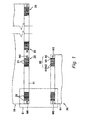
- a structure of a liquid crystal cell 10 is the same as that of the liquid crystal cell described by referring to Fig. 5 .
- lead-out electrode rows 20 are formed on an edge part of a glass substrate 11 of one side of the liquid crystal cell 10.
- many lead-out electrodes 21 densely arranged in parallel at equal pitches P1 are included.
- lead terminal rows 60 are formed on an edge part of a rectangular base film 51 on which a liquid crystal control circuit (not shown in the drawing) including an IC chip is formed.
- a liquid crystal control circuit (not shown in the drawing) including an IC chip is formed.
- many practical lead terminals 61 arranged in parallel and a prescribed number of dummy terminals 65 are included.
- two dummy terminals 65 and 65 are adjacently arranged in parallel.
- the dummy terminals 65 and 65 have the same sizes as those of the practical lead terminals 61.
- the practical lead terminals 61 are used for actually forming a signal path.
- the dummy terminals 65 are not actually used for forming the signal path.
- Fig. 1 the illustrations of the lead-out electrodes 21 or the practical lead terminals 61 located in an intermediate part in the direction of an arrangement are omitted. Further, a hatching is applied to the dummy terminals 65 and 65.
- alignment marks M1 and M2 are respectively attached to the above-described liquid crystal cell 10 and the flexible relay board 50.
- the alignment marks M1 and M2 are located at both sides sandwiching the above-described lead-out electrodes row 20 and at both sides sandwiching the lead terminal row 60.
- a correction of an extension considering the extension percentage of the base film 51 in a thermal compression bonding process is applied only in the positions of the practical lead terminals 61 of the lead terminal rows 60 in the flexible relay board 50 side. Accordingly, the correction of the extension is not applied to the positions of the two dummy terminals 65 and 65 respectively located at both the sides in the row ends of the practical lead terminal row 62.
- pitches P3 between the practical lead terminals 61 in the flexible relay board 50 side are narrower than the pitches P1 between the lead-out electrodes 21 of the liquid crystal cell 10 side.
- pitches P4 between the two dummy terminals 65 and 65 at the row ends in the flexible relay board side 50 have the same values as those of the pitches P1 between the lead-out electrodes 21 in the liquid crystal cell 10 side.
- the two dummy terminals 65 and 65 at the row ends of the flexible relay board 50 side are individually overlapped on the two lead-out electrodes 21 and 21 located in row ends of the lead-out electrode rows 20 in the liquid crystal cell 10 side.
- an operator visually decides the suitability of the overlapped state of the two dummy terminals 65 and 65 and the two lead-out electrodes 21 and 21 which are enlarged and displayed on a monitor.
- the practical lead terminal 61 at the row end of the practical lead terminal row 62 in the flexible relay board 50 side is located more inside of the flexible relay board 50 by an amount shown by a sign ⁇ 1 than a third lead-out electrode 21 from the row end in the liquid crystal cell 10 side.
- the positioning process can be easily carried out with a higher accuracy than that when the overlapped state of the alignment marks M1 and M2 is visually decided as described in the usual example.
- the base film 51 of the flexible relay board 50 is extended by an amount meeting the extension percentage thereof as shown by an arrow mark A.
- the individual practical lead terminals 61 in the flexible relay board 50 side are separately thermally compression boded to and electrically connected to the individual lead-out electrodes 21 in the liquid crystal cell 10 side.
- the dummy terminals 65 are misaligned with the two lead-out electrodes 21 at the row ends in the liquid crystal cell 10 side via the thermal compression bonding process, since the dummy terminals 65 are terminals which are not originally used, the performance of the liquid crystal module is not adversely affected.
- an alignment mark M2 is misaligned with an alignment mark M1 in the liquid crystal cell 10 side, since the alignment marks M1 and M2 are not electric elements, the performance of the liquid crystal module is not adversely affected as mentioned above.
- the dummy terminals 65 of the flexible relay board 50 side are located respectively at both sides in the row ends of the lead terminal rows 60. According to this structure, the operator easily specifies the dummy terminals 65 in the lead terminal rows 60 of the flexible relay board 50. Further, the correction of the extension applied to the positions of the practical lead terminals 61 is easily designed or set
- the dummy terminals 65 may be located only in one row end of the lead terminal row 60.
- the two dummy terminals 65 are provided adjacent each other in the row end. According to this structure, since the operator can position the two dummy terminals 65 to the two lead-out electrodes 21 in the liquid crystal cell side, the accuracy in positioning is the more easily improved.
- the number of the dummy terminals 65 in the row end may be one or a number more than three.
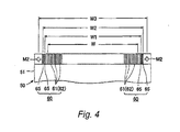
- a method for applying the correction of the extension to the positions of the practical lead terminals 61, a method is employed in which a space dimension W between the two practical lead terminals 61 and 61 located at both the sides In the row ends of the practical lead terminal row 62 is shortened by considering the extension percentage of the base film 51 in the thermal compression bonding process. According to this method, the correction of the extension applied to the positions of the practical lead terminals 61 is advantageously easily designed and set.
- W1 designates a space dimension between second dummy terminals 65 and 65 at both the sides in the row ends of the lead terminal row 60
- W2 designates a space dimension between the dummy terminals 65 and 65 at both the sides in the row ends of the lead terminal row 60
- W3 designates a space dimension between the alignment marks M2 and M2 at both the sides of the lead terminal row 60.
- the dummy terminals 65 which can be used for the positioning process are provided in place of the alignment mark M2, but also the alignment mark M2 is provided. Accordingly, when the positioning process is carried out, both the dummy terminals 65 and the alignment mark M2 may be used. Further, the alignment mark M2 may be omitted.
Landscapes
- Physics & Mathematics (AREA)
- Nonlinear Science (AREA)
- Engineering & Computer Science (AREA)
- Mathematical Physics (AREA)
- Chemical & Material Sciences (AREA)
- Crystallography & Structural Chemistry (AREA)
- General Physics & Mathematics (AREA)
- Optics & Photonics (AREA)
- Manufacturing & Machinery (AREA)
- Microelectronics & Electronic Packaging (AREA)
- Liquid Crystal (AREA)
- Devices For Indicating Variable Information By Combining Individual Elements (AREA)
Applications Claiming Priority (1)
| Application Number | Priority Date | Filing Date | Title |
|---|---|---|---|
| JP2009089172A JP2010243585A (ja) | 2009-04-01 | 2009-04-01 | 液晶モジュール |
Publications (1)
| Publication Number | Publication Date |
|---|---|
| EP2237101A1 true EP2237101A1 (de) | 2010-10-06 |
Family
ID=42232783
Family Applications (1)
| Application Number | Title | Priority Date | Filing Date |
|---|---|---|---|
| EP10158556A Ceased EP2237101A1 (de) | 2009-04-01 | 2010-03-31 | Flüssigkristallmodul |
Country Status (3)
| Country | Link |
|---|---|
| US (1) | US8203684B2 (de) |
| EP (1) | EP2237101A1 (de) |
| JP (1) | JP2010243585A (de) |
Cited By (3)
| Publication number | Priority date | Publication date | Assignee | Title |
|---|---|---|---|---|
| EP2337434A1 (de) * | 2009-12-21 | 2011-06-22 | Funai Electric Co., Ltd. | Anordnungsverfahren einer Flüssigkristallanzeigevorrichtung und chipmontiertes Verdrahtungssubstrat für das Verfahren |
| CN104347008A (zh) * | 2013-07-26 | 2015-02-11 | 精工爱普生株式会社 | 安装结构、电光学装置以及电子设备 |
| CN110596970A (zh) * | 2019-08-27 | 2019-12-20 | 深圳市华星光电技术有限公司 | 一种显示面板及其制作方法、显示装置 |
Families Citing this family (2)
| Publication number | Priority date | Publication date | Assignee | Title |
|---|---|---|---|---|
| US8994898B2 (en) * | 2012-10-18 | 2015-03-31 | Shenzhen China Star Optoelectronics Technology Co., Ltd | COF base tape and manufacturing method thereof and liquid crystal display module comprising same |
| JP2015075559A (ja) | 2013-10-08 | 2015-04-20 | 株式会社ジャパンディスプレイ | 電子装置 |
Citations (7)
| Publication number | Priority date | Publication date | Assignee | Title |
|---|---|---|---|---|
| JPS613126A (ja) * | 1984-06-15 | 1986-01-09 | Citizen Watch Co Ltd | 液晶表示装置 |
| JPH04287022A (ja) * | 1991-03-15 | 1992-10-12 | Hitachi Ltd | 液晶表示装置 |
| JPH0521515A (ja) * | 1991-07-15 | 1993-01-29 | Seiko Epson Corp | 液晶表示デバイスとその製造方法 |
| US5258866A (en) * | 1991-03-18 | 1993-11-02 | Alps Electric Co., Ltd. | Method of connecting liquid crystal display and circuit board with thermal expansion compensation |
| JP2000312070A (ja) | 1999-04-27 | 2000-11-07 | Optrex Corp | 電極端子の接続方法 |
| JP2004087608A (ja) | 2002-08-23 | 2004-03-18 | Sharp Corp | フレキシブル基板およびそれを用いたlcdモジュール |
| US20070246836A1 (en) * | 2006-04-19 | 2007-10-25 | Ichiyama Iwane | Electric terminal device and method of connecting the same |
Family Cites Families (4)
| Publication number | Priority date | Publication date | Assignee | Title |
|---|---|---|---|---|
| JPH06152112A (ja) * | 1992-11-12 | 1994-05-31 | Matsushita Electric Ind Co Ltd | 回路の接続方法 |
| JPH07270816A (ja) * | 1994-04-01 | 1995-10-20 | Enplas Corp | 液晶パネル検査用コンタクト装置 |
| JPH09246676A (ja) * | 1996-03-04 | 1997-09-19 | Toshiba Corp | フレキシブル基板及びそれを用いた表示装置 |
| JP2002032030A (ja) * | 2000-05-12 | 2002-01-31 | Seiko Epson Corp | 電気光学装置の製造方法、端子の接続方法、電気光学装置および電子機器 |
-
2009
- 2009-04-01 JP JP2009089172A patent/JP2010243585A/ja active Pending
-
2010
- 2010-03-31 US US12/751,487 patent/US8203684B2/en not_active Expired - Fee Related
- 2010-03-31 EP EP10158556A patent/EP2237101A1/de not_active Ceased
Patent Citations (7)
| Publication number | Priority date | Publication date | Assignee | Title |
|---|---|---|---|---|
| JPS613126A (ja) * | 1984-06-15 | 1986-01-09 | Citizen Watch Co Ltd | 液晶表示装置 |
| JPH04287022A (ja) * | 1991-03-15 | 1992-10-12 | Hitachi Ltd | 液晶表示装置 |
| US5258866A (en) * | 1991-03-18 | 1993-11-02 | Alps Electric Co., Ltd. | Method of connecting liquid crystal display and circuit board with thermal expansion compensation |
| JPH0521515A (ja) * | 1991-07-15 | 1993-01-29 | Seiko Epson Corp | 液晶表示デバイスとその製造方法 |
| JP2000312070A (ja) | 1999-04-27 | 2000-11-07 | Optrex Corp | 電極端子の接続方法 |
| JP2004087608A (ja) | 2002-08-23 | 2004-03-18 | Sharp Corp | フレキシブル基板およびそれを用いたlcdモジュール |
| US20070246836A1 (en) * | 2006-04-19 | 2007-10-25 | Ichiyama Iwane | Electric terminal device and method of connecting the same |
Cited By (6)
| Publication number | Priority date | Publication date | Assignee | Title |
|---|---|---|---|---|
| EP2337434A1 (de) * | 2009-12-21 | 2011-06-22 | Funai Electric Co., Ltd. | Anordnungsverfahren einer Flüssigkristallanzeigevorrichtung und chipmontiertes Verdrahtungssubstrat für das Verfahren |
| US8615871B2 (en) | 2009-12-21 | 2013-12-31 | Funai Electric Co., Ltd. | Chip mounted wiring substrate |
| CN104347008A (zh) * | 2013-07-26 | 2015-02-11 | 精工爱普生株式会社 | 安装结构、电光学装置以及电子设备 |
| CN104347008B (zh) * | 2013-07-26 | 2019-10-01 | 精工爱普生株式会社 | 安装结构、电光学装置以及电子设备 |
| CN110596970A (zh) * | 2019-08-27 | 2019-12-20 | 深圳市华星光电技术有限公司 | 一种显示面板及其制作方法、显示装置 |
| US11372289B2 (en) | 2019-08-27 | 2022-06-28 | Tcl China Star Optoelectronics Technology Co., Ltd. | Display panel comprising at least one binding alignment block having a thickness greater than a thickness of each of a plurality of binding pins and method of manufacturing the same |
Also Published As
| Publication number | Publication date |
|---|---|
| JP2010243585A (ja) | 2010-10-28 |
| US8203684B2 (en) | 2012-06-19 |
| US20100253900A1 (en) | 2010-10-07 |
Similar Documents
| Publication | Publication Date | Title |
|---|---|---|
| KR0144283B1 (ko) | 리워킹이 용이한 소형경량 표시장치 및 그 실장방법 | |
| KR100556642B1 (ko) | 가요성 기판 및 그를 이용한 lcd 모듈 및 그 제조 방법 | |
| US7372514B2 (en) | Active matrix type display device having antistatic lines used as repair lines | |
| CN110191578B (zh) | 一种柔性电路板及测试治具 | |
| US8824150B2 (en) | Driving printed circuit board and liquid crystal display device including the same | |
| EP2164310A1 (de) | Anzeigemodul, flüssigkristallanzeigevorrichtung und verfahren zur herstellung eines anzeigemoduls | |
| US7349054B2 (en) | Method of mounting flexible circuit boards, and display device | |
| JPWO2000054098A1 (ja) | 液晶表示装置およびその検査方法 | |
| US8203684B2 (en) | Liquid crystal module | |
| CN110967880B (zh) | 显示面板及显示装置 | |
| JP2002314212A (ja) | フレキシブルプリント回路と配線基板との接続構造、その接続方法、液晶表示装置及びその製造方法 | |
| KR101160076B1 (ko) | 패널 테스트를 위한 필름타입 프로브블록 | |
| KR20160087944A (ko) | 인쇄 회로 기판 유닛, 표시 장치 및 표시 장치의 제조 방법 | |
| KR100756902B1 (ko) | Tft 기판, 필름 캐리어 및 액정표시소자의 제조방법 | |
| US20080119069A1 (en) | Board device and board | |
| KR101586334B1 (ko) | 패널 검사장치 | |
| JP5526756B2 (ja) | 液晶表示装置の実装方法及びそれに適するチップ搭載配線基板 | |
| EP2128685A1 (de) | Flüssigkristallanzeigevorrichtung und Verfahren zur Herstellung der Flüssigkristallanzeigevorrichtung | |
| US8975756B2 (en) | Electric terminal device and method of connecting the same | |
| JPH06202132A (ja) | パネルの実装構造 | |
| JP2001228806A (ja) | 平面表示装置 | |
| JPH07183634A (ja) | パネルの実装構造および実装方法並びにフレキシブル配線板並びに駆動ic交換方法 | |
| KR101485525B1 (ko) | 패널 검사장치 | |
| JP3251163B2 (ja) | 表示パネル検査装置 | |
| JP2002009412A (ja) | フレキシブル基板の接続方法及び接続構造並びに表示装置 |
Legal Events
| Date | Code | Title | Description |
|---|---|---|---|
| PUAI | Public reference made under article 153(3) epc to a published international application that has entered the european phase |
Free format text: ORIGINAL CODE: 0009012 |
|
| AK | Designated contracting states |
Kind code of ref document: A1 Designated state(s): AT BE BG CH CY CZ DE DK EE ES FI FR GB GR HR HU IE IS IT LI LT LU LV MC MK MT NL NO PL PT RO SE SI SK SM TR |
|
| AX | Request for extension of the european patent |
Extension state: AL BA ME RS |
|
| 17P | Request for examination filed |
Effective date: 20110131 |
|
| 17Q | First examination report despatched |
Effective date: 20110526 |
|
| STAA | Information on the status of an ep patent application or granted ep patent |
Free format text: STATUS: THE APPLICATION HAS BEEN REFUSED |
|
| 18R | Application refused |
Effective date: 20120613 |