EP2213639B1 - Monobenzochrysenderivat und verwendung in materialien für organische elektrolumineszenzvorrichtungen - Google Patents
Monobenzochrysenderivat und verwendung in materialien für organische elektrolumineszenzvorrichtungen Download PDFInfo
- Publication number
- EP2213639B1 EP2213639B1 EP08852665.2A EP08852665A EP2213639B1 EP 2213639 B1 EP2213639 B1 EP 2213639B1 EP 08852665 A EP08852665 A EP 08852665A EP 2213639 B1 EP2213639 B1 EP 2213639B1
- Authority
- EP
- European Patent Office
- Prior art keywords
- group
- substituted
- carbon atoms
- unsubstituted
- compound
- Prior art date
- Legal status (The legal status is an assumption and is not a legal conclusion. Google has not performed a legal analysis and makes no representation as to the accuracy of the status listed.)
- Active
Links
- 0 Cc1ccc2c(c(cccc3)c3c(*)c3)c3c3ccccc3c2c1 Chemical compound Cc1ccc2c(c(cccc3)c3c(*)c3)c3c3ccccc3c2c1 0.000 description 5
- YBNILZGAILBXRY-DEOSSOPVSA-N BC([C@@H]12)=Cc(c(cccc3)c3c3c4cccc3)c4C3=C1C2=CCC#C3 Chemical compound BC([C@@H]12)=Cc(c(cccc3)c3c3c4cccc3)c4C3=C1C2=CCC#C3 YBNILZGAILBXRY-DEOSSOPVSA-N 0.000 description 1
- QLTVJZSHTLMZSG-UHFFFAOYSA-N C(C1C=C2)C1c(c1c3)c2[o]c1ccc3-c(cc1)ccc1-c1cc(c(cccc2)c2c2c3cccc2)c3c2c1cccc2 Chemical compound C(C1C=C2)C1c(c1c3)c2[o]c1ccc3-c(cc1)ccc1-c1cc(c(cccc2)c2c2c3cccc2)c3c2c1cccc2 QLTVJZSHTLMZSG-UHFFFAOYSA-N 0.000 description 1
- KSNWNECQJNVLQA-UHFFFAOYSA-N Cc1c(cc(cc2)-c3cc(c(cccc4)c4c4ccccc44)c4c4c3cccc4)c2cc(-c2ccccc2)c1 Chemical compound Cc1c(cc(cc2)-c3cc(c(cccc4)c4c4ccccc44)c4c4c3cccc4)c2cc(-c2ccccc2)c1 KSNWNECQJNVLQA-UHFFFAOYSA-N 0.000 description 1
- VFUDMQLBKNMONU-UHFFFAOYSA-N c(cc1)cc(c2ccccc22)c1[n]2-c(cc1)ccc1-c(cc1)ccc1-[n]1c(cccc2)c2c2c1cccc2 Chemical compound c(cc1)cc(c2ccccc22)c1[n]2-c(cc1)ccc1-c(cc1)ccc1-[n]1c(cccc2)c2c2c1cccc2 VFUDMQLBKNMONU-UHFFFAOYSA-N 0.000 description 1
Images
Classifications
-
- H—ELECTRICITY
- H10—SEMICONDUCTOR DEVICES; ELECTRIC SOLID-STATE DEVICES NOT OTHERWISE PROVIDED FOR
- H10K—ORGANIC ELECTRIC SOLID-STATE DEVICES
- H10K85/00—Organic materials used in the body or electrodes of devices covered by this subclass
- H10K85/60—Organic compounds having low molecular weight
- H10K85/615—Polycyclic condensed aromatic hydrocarbons, e.g. anthracene
-
- H—ELECTRICITY
- H10—SEMICONDUCTOR DEVICES; ELECTRIC SOLID-STATE DEVICES NOT OTHERWISE PROVIDED FOR
- H10K—ORGANIC ELECTRIC SOLID-STATE DEVICES
- H10K85/00—Organic materials used in the body or electrodes of devices covered by this subclass
- H10K85/60—Organic compounds having low molecular weight
- H10K85/615—Polycyclic condensed aromatic hydrocarbons, e.g. anthracene
- H10K85/623—Polycyclic condensed aromatic hydrocarbons, e.g. anthracene containing five rings, e.g. pentacene
-
- C—CHEMISTRY; METALLURGY
- C07—ORGANIC CHEMISTRY
- C07C—ACYCLIC OR CARBOCYCLIC COMPOUNDS
- C07C13/00—Cyclic hydrocarbons containing rings other than, or in addition to, six-membered aromatic rings
- C07C13/28—Polycyclic hydrocarbons or acyclic hydrocarbon derivatives thereof
- C07C13/32—Polycyclic hydrocarbons or acyclic hydrocarbon derivatives thereof with condensed rings
- C07C13/54—Polycyclic hydrocarbons or acyclic hydrocarbon derivatives thereof with condensed rings with three condensed rings
- C07C13/547—Polycyclic hydrocarbons or acyclic hydrocarbon derivatives thereof with condensed rings with three condensed rings at least one ring not being six-membered, the other rings being at the most six-membered
- C07C13/567—Polycyclic hydrocarbons or acyclic hydrocarbon derivatives thereof with condensed rings with three condensed rings at least one ring not being six-membered, the other rings being at the most six-membered with a fluorene or hydrogenated fluorene ring system
-
- C—CHEMISTRY; METALLURGY
- C07—ORGANIC CHEMISTRY
- C07C—ACYCLIC OR CARBOCYCLIC COMPOUNDS
- C07C15/00—Cyclic hydrocarbons containing only six-membered aromatic rings as cyclic parts
- C07C15/20—Polycyclic condensed hydrocarbons
-
- C—CHEMISTRY; METALLURGY
- C07—ORGANIC CHEMISTRY
- C07D—HETEROCYCLIC COMPOUNDS
- C07D307/00—Heterocyclic compounds containing five-membered rings having one oxygen atom as the only ring hetero atom
- C07D307/77—Heterocyclic compounds containing five-membered rings having one oxygen atom as the only ring hetero atom ortho- or peri-condensed with carbocyclic rings or ring systems
- C07D307/91—Dibenzofurans; Hydrogenated dibenzofurans
-
- C—CHEMISTRY; METALLURGY
- C07—ORGANIC CHEMISTRY
- C07D—HETEROCYCLIC COMPOUNDS
- C07D333/00—Heterocyclic compounds containing five-membered rings having one sulfur atom as the only ring hetero atom
- C07D333/02—Heterocyclic compounds containing five-membered rings having one sulfur atom as the only ring hetero atom not condensed with other rings
- C07D333/04—Heterocyclic compounds containing five-membered rings having one sulfur atom as the only ring hetero atom not condensed with other rings not substituted on the ring sulphur atom
- C07D333/06—Heterocyclic compounds containing five-membered rings having one sulfur atom as the only ring hetero atom not condensed with other rings not substituted on the ring sulphur atom with only hydrogen atoms, hydrocarbon or substituted hydrocarbon radicals, directly attached to the ring carbon atoms
- C07D333/08—Hydrogen atoms or radicals containing only hydrogen and carbon atoms
-
- C—CHEMISTRY; METALLURGY
- C07—ORGANIC CHEMISTRY
- C07D—HETEROCYCLIC COMPOUNDS
- C07D333/00—Heterocyclic compounds containing five-membered rings having one sulfur atom as the only ring hetero atom
- C07D333/50—Heterocyclic compounds containing five-membered rings having one sulfur atom as the only ring hetero atom condensed with carbocyclic rings or ring systems
- C07D333/76—Dibenzothiophenes
-
- C—CHEMISTRY; METALLURGY
- C09—DYES; PAINTS; POLISHES; NATURAL RESINS; ADHESIVES; COMPOSITIONS NOT OTHERWISE PROVIDED FOR; APPLICATIONS OF MATERIALS NOT OTHERWISE PROVIDED FOR
- C09B—ORGANIC DYES OR CLOSELY-RELATED COMPOUNDS FOR PRODUCING DYES, e.g. PIGMENTS; MORDANTS; LAKES
- C09B1/00—Dyes with anthracene nucleus not condensed with any other ring
-
- C—CHEMISTRY; METALLURGY
- C09—DYES; PAINTS; POLISHES; NATURAL RESINS; ADHESIVES; COMPOSITIONS NOT OTHERWISE PROVIDED FOR; APPLICATIONS OF MATERIALS NOT OTHERWISE PROVIDED FOR
- C09B—ORGANIC DYES OR CLOSELY-RELATED COMPOUNDS FOR PRODUCING DYES, e.g. PIGMENTS; MORDANTS; LAKES
- C09B57/00—Other synthetic dyes of known constitution
-
- C—CHEMISTRY; METALLURGY
- C09—DYES; PAINTS; POLISHES; NATURAL RESINS; ADHESIVES; COMPOSITIONS NOT OTHERWISE PROVIDED FOR; APPLICATIONS OF MATERIALS NOT OTHERWISE PROVIDED FOR
- C09K—MATERIALS FOR MISCELLANEOUS APPLICATIONS, NOT PROVIDED FOR ELSEWHERE
- C09K11/00—Luminescent materials, e.g. electroluminescent or chemiluminescent
- C09K11/06—Luminescent materials, e.g. electroluminescent or chemiluminescent containing organic luminescent materials
-
- H—ELECTRICITY
- H05—ELECTRIC TECHNIQUES NOT OTHERWISE PROVIDED FOR
- H05B—ELECTRIC HEATING; ELECTRIC LIGHT SOURCES NOT OTHERWISE PROVIDED FOR; CIRCUIT ARRANGEMENTS FOR ELECTRIC LIGHT SOURCES, IN GENERAL
- H05B33/00—Electroluminescent light sources
- H05B33/12—Light sources with substantially two-dimensional [2D] radiating surfaces
- H05B33/14—Light sources with substantially two-dimensional [2D] radiating surfaces characterised by the chemical or physical composition or the arrangement of the electroluminescent material, or by the simultaneous addition of the electroluminescent material in or onto the light source
-
- H—ELECTRICITY
- H05—ELECTRIC TECHNIQUES NOT OTHERWISE PROVIDED FOR
- H05B—ELECTRIC HEATING; ELECTRIC LIGHT SOURCES NOT OTHERWISE PROVIDED FOR; CIRCUIT ARRANGEMENTS FOR ELECTRIC LIGHT SOURCES, IN GENERAL
- H05B33/00—Electroluminescent light sources
- H05B33/12—Light sources with substantially two-dimensional [2D] radiating surfaces
- H05B33/20—Light sources with substantially two-dimensional [2D] radiating surfaces characterised by the chemical or physical composition or the arrangement of the material in which the electroluminescent material is embedded
-
- H—ELECTRICITY
- H10—SEMICONDUCTOR DEVICES; ELECTRIC SOLID-STATE DEVICES NOT OTHERWISE PROVIDED FOR
- H10K—ORGANIC ELECTRIC SOLID-STATE DEVICES
- H10K50/00—Organic light-emitting devices
- H10K50/10—OLEDs or polymer light-emitting diodes [PLED]
- H10K50/11—OLEDs or polymer light-emitting diodes [PLED] characterised by the electroluminescent [EL] layers
-
- H—ELECTRICITY
- H10—SEMICONDUCTOR DEVICES; ELECTRIC SOLID-STATE DEVICES NOT OTHERWISE PROVIDED FOR
- H10K—ORGANIC ELECTRIC SOLID-STATE DEVICES
- H10K85/00—Organic materials used in the body or electrodes of devices covered by this subclass
- H10K85/60—Organic compounds having low molecular weight
- H10K85/615—Polycyclic condensed aromatic hydrocarbons, e.g. anthracene
- H10K85/626—Polycyclic condensed aromatic hydrocarbons, e.g. anthracene containing more than one polycyclic condensed aromatic rings, e.g. bis-anthracene
-
- C—CHEMISTRY; METALLURGY
- C07—ORGANIC CHEMISTRY
- C07C—ACYCLIC OR CARBOCYCLIC COMPOUNDS
- C07C2603/00—Systems containing at least three condensed rings
- C07C2603/02—Ortho- or ortho- and peri-condensed systems
- C07C2603/04—Ortho- or ortho- and peri-condensed systems containing three rings
- C07C2603/06—Ortho- or ortho- and peri-condensed systems containing three rings containing at least one ring with less than six ring members
- C07C2603/10—Ortho- or ortho- and peri-condensed systems containing three rings containing at least one ring with less than six ring members containing five-membered rings
-
- C—CHEMISTRY; METALLURGY
- C07—ORGANIC CHEMISTRY
- C07C—ACYCLIC OR CARBOCYCLIC COMPOUNDS
- C07C2603/00—Systems containing at least three condensed rings
- C07C2603/02—Ortho- or ortho- and peri-condensed systems
- C07C2603/04—Ortho- or ortho- and peri-condensed systems containing three rings
- C07C2603/06—Ortho- or ortho- and peri-condensed systems containing three rings containing at least one ring with less than six ring members
- C07C2603/10—Ortho- or ortho- and peri-condensed systems containing three rings containing at least one ring with less than six ring members containing five-membered rings
- C07C2603/12—Ortho- or ortho- and peri-condensed systems containing three rings containing at least one ring with less than six ring members containing five-membered rings only one five-membered ring
- C07C2603/18—Fluorenes; Hydrogenated fluorenes
-
- C—CHEMISTRY; METALLURGY
- C07—ORGANIC CHEMISTRY
- C07C—ACYCLIC OR CARBOCYCLIC COMPOUNDS
- C07C2603/00—Systems containing at least three condensed rings
- C07C2603/02—Ortho- or ortho- and peri-condensed systems
- C07C2603/04—Ortho- or ortho- and peri-condensed systems containing three rings
- C07C2603/22—Ortho- or ortho- and peri-condensed systems containing three rings containing only six-membered rings
- C07C2603/26—Phenanthrenes; Hydrogenated phenanthrenes
-
- C—CHEMISTRY; METALLURGY
- C07—ORGANIC CHEMISTRY
- C07C—ACYCLIC OR CARBOCYCLIC COMPOUNDS
- C07C2603/00—Systems containing at least three condensed rings
- C07C2603/02—Ortho- or ortho- and peri-condensed systems
- C07C2603/40—Ortho- or ortho- and peri-condensed systems containing four condensed rings
- C07C2603/42—Ortho- or ortho- and peri-condensed systems containing four condensed rings containing only six-membered rings
- C07C2603/50—Pyrenes; Hydrogenated pyrenes
-
- C—CHEMISTRY; METALLURGY
- C07—ORGANIC CHEMISTRY
- C07C—ACYCLIC OR CARBOCYCLIC COMPOUNDS
- C07C2603/00—Systems containing at least three condensed rings
- C07C2603/02—Ortho- or ortho- and peri-condensed systems
- C07C2603/52—Ortho- or ortho- and peri-condensed systems containing five condensed rings
-
- C—CHEMISTRY; METALLURGY
- C09—DYES; PAINTS; POLISHES; NATURAL RESINS; ADHESIVES; COMPOSITIONS NOT OTHERWISE PROVIDED FOR; APPLICATIONS OF MATERIALS NOT OTHERWISE PROVIDED FOR
- C09K—MATERIALS FOR MISCELLANEOUS APPLICATIONS, NOT PROVIDED FOR ELSEWHERE
- C09K2211/00—Chemical nature of organic luminescent or tenebrescent compounds
- C09K2211/10—Non-macromolecular compounds
- C09K2211/1003—Carbocyclic compounds
- C09K2211/1007—Non-condensed systems
-
- C—CHEMISTRY; METALLURGY
- C09—DYES; PAINTS; POLISHES; NATURAL RESINS; ADHESIVES; COMPOSITIONS NOT OTHERWISE PROVIDED FOR; APPLICATIONS OF MATERIALS NOT OTHERWISE PROVIDED FOR
- C09K—MATERIALS FOR MISCELLANEOUS APPLICATIONS, NOT PROVIDED FOR ELSEWHERE
- C09K2211/00—Chemical nature of organic luminescent or tenebrescent compounds
- C09K2211/10—Non-macromolecular compounds
- C09K2211/1003—Carbocyclic compounds
- C09K2211/1011—Condensed systems
-
- C—CHEMISTRY; METALLURGY
- C09—DYES; PAINTS; POLISHES; NATURAL RESINS; ADHESIVES; COMPOSITIONS NOT OTHERWISE PROVIDED FOR; APPLICATIONS OF MATERIALS NOT OTHERWISE PROVIDED FOR
- C09K—MATERIALS FOR MISCELLANEOUS APPLICATIONS, NOT PROVIDED FOR ELSEWHERE
- C09K2211/00—Chemical nature of organic luminescent or tenebrescent compounds
- C09K2211/10—Non-macromolecular compounds
- C09K2211/1018—Heterocyclic compounds
- C09K2211/1025—Heterocyclic compounds characterised by ligands
- C09K2211/1088—Heterocyclic compounds characterised by ligands containing oxygen as the only heteroatom
-
- C—CHEMISTRY; METALLURGY
- C09—DYES; PAINTS; POLISHES; NATURAL RESINS; ADHESIVES; COMPOSITIONS NOT OTHERWISE PROVIDED FOR; APPLICATIONS OF MATERIALS NOT OTHERWISE PROVIDED FOR
- C09K—MATERIALS FOR MISCELLANEOUS APPLICATIONS, NOT PROVIDED FOR ELSEWHERE
- C09K2211/00—Chemical nature of organic luminescent or tenebrescent compounds
- C09K2211/10—Non-macromolecular compounds
- C09K2211/1018—Heterocyclic compounds
- C09K2211/1025—Heterocyclic compounds characterised by ligands
- C09K2211/1092—Heterocyclic compounds characterised by ligands containing sulfur as the only heteroatom
-
- C—CHEMISTRY; METALLURGY
- C09—DYES; PAINTS; POLISHES; NATURAL RESINS; ADHESIVES; COMPOSITIONS NOT OTHERWISE PROVIDED FOR; APPLICATIONS OF MATERIALS NOT OTHERWISE PROVIDED FOR
- C09K—MATERIALS FOR MISCELLANEOUS APPLICATIONS, NOT PROVIDED FOR ELSEWHERE
- C09K2211/00—Chemical nature of organic luminescent or tenebrescent compounds
- C09K2211/14—Macromolecular compounds
- C09K2211/1408—Carbocyclic compounds
- C09K2211/1416—Condensed systems
-
- H—ELECTRICITY
- H10—SEMICONDUCTOR DEVICES; ELECTRIC SOLID-STATE DEVICES NOT OTHERWISE PROVIDED FOR
- H10K—ORGANIC ELECTRIC SOLID-STATE DEVICES
- H10K2102/00—Constructional details relating to the organic devices covered by this subclass
-
- H—ELECTRICITY
- H10—SEMICONDUCTOR DEVICES; ELECTRIC SOLID-STATE DEVICES NOT OTHERWISE PROVIDED FOR
- H10K—ORGANIC ELECTRIC SOLID-STATE DEVICES
- H10K85/00—Organic materials used in the body or electrodes of devices covered by this subclass
- H10K85/30—Coordination compounds
- H10K85/341—Transition metal complexes, e.g. Ru(II)polypyridine complexes
- H10K85/342—Transition metal complexes, e.g. Ru(II)polypyridine complexes comprising iridium
-
- H—ELECTRICITY
- H10—SEMICONDUCTOR DEVICES; ELECTRIC SOLID-STATE DEVICES NOT OTHERWISE PROVIDED FOR
- H10K—ORGANIC ELECTRIC SOLID-STATE DEVICES
- H10K85/00—Organic materials used in the body or electrodes of devices covered by this subclass
- H10K85/30—Coordination compounds
- H10K85/341—Transition metal complexes, e.g. Ru(II)polypyridine complexes
- H10K85/346—Transition metal complexes, e.g. Ru(II)polypyridine complexes comprising platinum
-
- H—ELECTRICITY
- H10—SEMICONDUCTOR DEVICES; ELECTRIC SOLID-STATE DEVICES NOT OTHERWISE PROVIDED FOR
- H10K—ORGANIC ELECTRIC SOLID-STATE DEVICES
- H10K85/00—Organic materials used in the body or electrodes of devices covered by this subclass
- H10K85/60—Organic compounds having low molecular weight
- H10K85/615—Polycyclic condensed aromatic hydrocarbons, e.g. anthracene
- H10K85/622—Polycyclic condensed aromatic hydrocarbons, e.g. anthracene containing four rings, e.g. pyrene
-
- H—ELECTRICITY
- H10—SEMICONDUCTOR DEVICES; ELECTRIC SOLID-STATE DEVICES NOT OTHERWISE PROVIDED FOR
- H10K—ORGANIC ELECTRIC SOLID-STATE DEVICES
- H10K85/00—Organic materials used in the body or electrodes of devices covered by this subclass
- H10K85/60—Organic compounds having low molecular weight
- H10K85/631—Amine compounds having at least two aryl rest on at least one amine-nitrogen atom, e.g. triphenylamine
-
- H—ELECTRICITY
- H10—SEMICONDUCTOR DEVICES; ELECTRIC SOLID-STATE DEVICES NOT OTHERWISE PROVIDED FOR
- H10K—ORGANIC ELECTRIC SOLID-STATE DEVICES
- H10K85/00—Organic materials used in the body or electrodes of devices covered by this subclass
- H10K85/60—Organic compounds having low molecular weight
- H10K85/649—Aromatic compounds comprising a hetero atom
- H10K85/657—Polycyclic condensed heteroaromatic hydrocarbons
-
- Y—GENERAL TAGGING OF NEW TECHNOLOGICAL DEVELOPMENTS; GENERAL TAGGING OF CROSS-SECTIONAL TECHNOLOGIES SPANNING OVER SEVERAL SECTIONS OF THE IPC; TECHNICAL SUBJECTS COVERED BY FORMER USPC CROSS-REFERENCE ART COLLECTIONS [XRACs] AND DIGESTS
- Y02—TECHNOLOGIES OR APPLICATIONS FOR MITIGATION OR ADAPTATION AGAINST CLIMATE CHANGE
- Y02B—CLIMATE CHANGE MITIGATION TECHNOLOGIES RELATED TO BUILDINGS, e.g. HOUSING, HOUSE APPLIANCES OR RELATED END-USER APPLICATIONS
- Y02B20/00—Energy efficient lighting technologies, e.g. halogen lamps or gas discharge lamps
- Y02B20/30—Semiconductor lamps, e.g. solid state lamps [SSL] light emitting diodes [LED] or organic LED [OLED]
-
- Y—GENERAL TAGGING OF NEW TECHNOLOGICAL DEVELOPMENTS; GENERAL TAGGING OF CROSS-SECTIONAL TECHNOLOGIES SPANNING OVER SEVERAL SECTIONS OF THE IPC; TECHNICAL SUBJECTS COVERED BY FORMER USPC CROSS-REFERENCE ART COLLECTIONS [XRACs] AND DIGESTS
- Y10—TECHNICAL SUBJECTS COVERED BY FORMER USPC
- Y10S—TECHNICAL SUBJECTS COVERED BY FORMER USPC CROSS-REFERENCE ART COLLECTIONS [XRACs] AND DIGESTS
- Y10S428/00—Stock material or miscellaneous articles
- Y10S428/917—Electroluminescent
Definitions
- the invention relates to a novel fused aromatic ring derivative (monobenzochrysene derivative) which is useful as a material for an organic electroluminescence device, and an organic electroluminescence device using the same.
- An organic electroluminescence device (hereinafter the term “electroluminescence” is often abbreviated as "EL”) is a self-emission device utilizing the principle that a fluorescent compound emits light by the recombination energy of holes injected from an anode and electrons injected from a cathode when an electric field is impressed.
- An organic EL device has made a remarkable progress.
- an organic EL device has characteristics such as low voltage driving, high luminance, variety in emission wavelength, high response and capability of fabricating a thin and lightweight emitting device, its application to a wide range of fields is expected.
- Emission materials used in an organic EL device have conventionally been studied actively since they influence largely the color of light emitted by a device or on emission life.
- a chelate complex such as tris(8-quinolinolato)aluminum complex, a coumarin derivative, a tetraphenylbutadiene derivative, a bisstyrylarylene derivative and an oxadiazole derivative are known.
- emission in a visible range from blue to red can be obtained.
- An organic EL device using polyphenylene vinylene (PPV) as a conjugated polymer is known.
- PPV polyphenylene vinylene
- this device PPV is applied and formed into a single film and this device is confirmed to emit light.
- An object of the invention is to provide an organic material which is suitable for use as a material of an organic EL device.
- the following monobenzochrysene derivative or the like can be provided.
- the organic EL device using the monobenzochrysene derivative of the invention has a long lifetime and a high efficiency, and is capable of being driven at a low voltage.
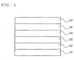
- FIG 1 is a schematic cross-sectional view of the organic EL device according to one embodiment of the invention.
- the monobenzochrysene derivative of the invention is a compound shown by the following formula (1): wherein R 1 to R 14 are independently a hydrogen atom or a substituent, and
- examples of the substituent shown by R 1 to R 14 include an alkyl group (one having preferably 1 to 20, more preferably 1 to 12 and particularly preferably 1 to 8 carbon atoms, the specific examples of which include methyl, ethyl, isopropyl, t-butyl, n-octyl, n-decyl, n-hexadecyl, cyclopropyl, cyclopentyl and cyclohexyl), an alkenyl group (one having preferably 2 to 20, more preferably 2 to 12 and particularly preferably 2 to 8 carbon atoms, the specific examples of which include vinyl, allyl, 2-butenyl and 3-pentenyl), an alkynyl group (one having preferably 2 to 20, more preferably 2 to 12 and particularly preferably 2 to 8 carbon atoms, the specific examples of which include propynyl and 3-pentynyl), a substituted or unsubstituted aryl-
- R 1 to R 14 is a substituted or unsubstituted aryl group having 6 to 50 (preferably 6 to 20, more preferably 6 to 14) ring carbon atoms which does not contain an anthracene skeleton and a benzo[g]chrysene skeleton or a substituted or unsubstituted heteroaryl group having 5 to 50 (preferably 5 to 20) ring carbon atoms which does not contain an anthracene skeleton and a benzo[g]chrysene skeleton.
- substituted or unsubstituted aryl group having 6 to 50 ring carbon atoms which does not contain an anthracene skeleton and a benzo[g]chrysene skeleton a phenyl group, 1-naphthyl group, 2-naphthyl group, 1-anthryl group, 2-anthryl group, 9-anthryl group, 1-phenanthryl group, 2-phenanthryl group, 3-phenanthryl group, 4-phenanthryl group, 9-phenanthryl group, 1-naphthacenyl group, 2-naphthacenyl group, 9-naphthacenyl group, 1-pyrenyl) group, 2-pyrenyl group, 4-pyrenyl group, 2-biphenylyl group, 3-biphenylyl group, 4-biphenylyl group, p-terphenyl-4-yl group, p-terphenyl-3-yl group, p-
- Preferred examples include a phenyl group, naphthyl group, phenanthryl, group, triphenylenyl group, pyrenyl group, benzanthranyl group, chrysenyl group, phenyl-1-napthyl group, phenyl-2-naphthyl group, naphthyl-1-naphthyl group, naphthyl-2-napthyl group and a substituent formed by combination of a plurality of these groups.
- substituted or unsubstituted heteroaryl group having 5 to 50 ring carbon atoms which does not contain an anthracene skeleton and a benzo[g]chrysene skeleton an imidazolyl group, pyridyl group, quinolyl group, piperidyl group, morpholino group, benzooxazolyl group, benzoimidazolyl group, benzothiazolyl group, carbazolyl group, and a monovalent group derived from a furan ring, thiophene ring, benzofuran ring, benzothiophene ring, dibenzofuran ring and dibenzothiophene ring can be given.
- Preferred examples include a monovalent group derived from a benzothiophene ring, a dibenzofuran ring and a dibenzothiophene ring.
- the substituents do not contain an anthracene skeleton and a benzo[g]chrysene skeleton.
- the monobenzochrysene derivative of the invention is preferably a compound shown by the following formulas (2) to (4):
- the single bond bonding the benzochrysene skeleton and the benzene skeleton may be bonded to any of the 14 bonding positions of the benzochrysene skeleton.
- R a may be bonded to any of the 14 bonding positions of the benzochrysene skeleton, and R b may be bonded to any of the 6 bonding positions of the benzene skeleton.
- Ar 1 may be bonded to any of the 6 bonding positions of the benzene skeleton.
- the substituents shown by R a , R b and R c , and the substituted or unsubstituted aryl group having 6 to 50 ring carbon atoms or the substituted or unsubstituted heteroaryl group having 5 to 50 ring carbon atoms shown by Ar 2 , Ar 3 and Ar 4 are the same as those in the formula (1).
- the monobenzochrysene derivative of the invention can be prepared by synthesizing benzo[g]chrysene with reference to the following literatures, halogenating the thus synthesized benzo[g]chrysene to prepare a halogenated benzo[g]chrysene, followed by a reaction with a boronic acid compound.
- the benzo[g]chrysene is the following compound. benzo[g]chrysene
- the monobenzochrysene derivative of the invention can be preferably used as a material for an organic EL device, in particular, as the emitting material thereof.
- the organic EL device of the invention comprises an anode, a cathode and one or more organic thin layers comprising an emitting layer between the anode and the cathode, and at least one of the organic thin layers comprise the above-mentioned compound of the invention.
- the representative examples of the configuration of the organic EL device of the invention are, however, not limited to the above. Of these, the configuration (8) is preferable.
- This organic EL device comprises an anode 10, a cathode 20, and a hole-injecting layer 30, a hole-transporting layer 32, an emitting layer 34 and an electron-injecting layer 36 between the anode and the cathode.
- the hole-injecting layer 30, the hole-transporting layer 32, the emitting layer 34 and the electron-injecting layer 36 correspond to the plurality of organic thin film layers. At least one of these organic thin film layers 30, 32, 34 and 36 comprises the compound of the invention.
- the compound of the invention may be used in any of the above-mentioned organic thin film layers, it is preferred that the compound of the invention be used in the emitting layer. In each of the organic thin film layers, the compound of the invention may be used either singly or in mixture with other compounds. In the device of the invention, it is preferred that the emitting layer contain the compound of the invention as a host material and contain at least one of a fluorescent dopant and a phosphorescent dopant.
- the emitting layer consist essentially of the compound of the invention and the above-mentioned dopant.
- the content of the compound of the invention in the organic thin film layers is preferably 30 to 100 mol%.
- the organic EL device is normally formed on a substrate.
- the substrate supports the organic EL device. It is preferable to use a smooth substrate. If light is outcoupled through the substrate, it is preferred that the substrate be a transparent substrate with a transmission to visible rays with a wavelength of 400 to 700 nm of 50% or more.
- a glass plate, a synthetic resin plate or the like are preferably used as such tranparent substrate.
- the glass plate include plates of soda-lime glass, barium/strontium-containing glass, lead glass, aluminosilicate glass, borosilicate glass, barium borosilicate glass, quartz, or the like.
- the synthetic resin plates include plates of a polycarbonate resin, an acrylic resin, a polyethylene terephthalate resin, a polyether sulfide resin, a polysulfone resin, or the like.
- the anode injects holes to the hole-injecting layer, the hole-transporting layer or the emitting layer and has a work function of 4.5 eV or more.
- the anode material include indium tin oxide (ITO), a mixture of indium oxide and zinc oxide, a mixture of ITO and cerium oxide (ITCO), a mixture of the mixture of indium oxide, and zinc oxide and cerium oxide (IZCO), a mixture of indium oxide and cerium oxide (ICO), a mixture of zinc oxide and aluminum oxide (AZO), tin oxide (NESA), gold, silver, platinum and copper.
- the anode can be formed from these electrode materials by a vapor deposition method, a sputtering method or the like.
- the transmittance of the anode to the emission is preferably more than 10%.
- the sheet resistance of the anode is preferably several hundred ⁇ / ⁇ or less.
- the film thickness of the anode which varies dependin g upon the material thereof, is usually from 10 nm to 1 ⁇ m, preferably from 10 to 200 nm.
- the emitting layer has the following functions.
- the emitting layer As the method of forming the emitting layer, a known method such as deposition, spin coating, or an LB method may be applied. It is preferable that the emitting layer be a molecular deposition film.
- the molecular deposition film is a film formed by deposition of a material compound in a gas phase, or by solidification of a material compound in the form of a solution or in a liquid phase.
- the molecular deposition film can be usually distinguished from a thin film (molecular accumulation film) formed using the LB method by the difference in aggregation structure or higher order structure or the difference in function due to the difference in structure.
- the emitting layer may also be formed by dissolving a binder such as a resin and a material compound in a solvent to obtain a solution, and forming a thin film from the solution by spin coating or the like.
- the emitting layer contain the compound of the invention as a host material.
- the emitting layer may contain, in addition to the compound of the invention, host materials given below.
- the emitting layer contain the compound of the invention as a host and contain at least one of a phosphorescent dopant and a fluorescent dopant.
- An emitting layer containing these dopants may be stacked on an emitting layer containing the compound of the invention.
- a phosphorescent dopant is a compound that can emit light from triplet excitons.
- the dopant is not limited so long as it can emit light from triplet excitons, but it is preferably a metal complex containing at least one metal selected from the group of Ir, Au, Cu, Ru, Pd, Pt, Os and Re: A porphyrin metal complex or an ortho-metalated metal complex is preferable.
- the phosphorescent compounds can be used individually or as a combination of two or more kinds.
- the above-mentioned phosphorescent dopant exhibit an emission spectrum having a maximum peak wavelength of 520 to 700 nm.
- porphyrin metal complex As a porphyrin metal complex, a porphyrin platinum complex is preferable.
- ligands forming an ortho-metalated metal complex.
- Preferable ligands include compounds having a phenylpyridine skeleton, a bipyridyl skeleton or a phenanthroline skeleton, 2-phenylpyridine, 7,8-benzoquinoline, 2-(2-thienyl)pyridine, 2-(1-naphthyl)pyridine and 2-phenylquinoline derivatives. These ligands may have a substituent, if necessary.
- Ligands to which fluorides, e.g. a trifluoromethyl group, being introduced as a substituent are particularly preferable as a blue dopant.
- auxiliary ligand preferred are ligands other than the above-mentioned ligands, such as acetylacetonate and picric acid may be contained.
- the content of a phosphorescent dopant in an emitting layer is not limited and can be properly selected according to purposes; for example, it is 0.1 to 70 mass %, preferably 1 to 30 (preferably 1 to 12) mass %.
- emission may be weak and the advantages thereof may not be sufficiently obtained.
- concentration quenching may significantly proceed, thereby degrading the device performance.
- the fluorescent dopant it is preferable to select a compound from amine-based compounds, aromatic compounds, chelate complexes such as tris(8-quinolilate)aluminum complexes, coumarin derivatives, tetraphenylbutadiene derivatives, bisstyrylarylene derivatives, oxadiazole derivatives or the like, taking into consideration required emission colors.
- styrylamine compounds, styryldiamine compounds, arylamine compounds and aryldiamine compounds are further preferable.
- Fused polycyclic aromatic compounds which are not an amine compound are also preferable.
- These fluorescent dopants may be used singly or in combination of two or more.
- the content of a fluorescent dopant in the emitting layer is not particularly limited and can be appropriately selected according to purposes; for example, it is 0.01 to 100 mass %, preferably 0.1 to 30 mass %.
- Ar 101 is a group with a valence of p corresponding to a phenyl group, a naphthyl-group, a biphenyl group, a terphenyl group, a stilbenyl group or a distyrylaryl group
- Ar 102 and Ar 103 are independently an aromatic hydrocarbon group having 6 to 20 (preferably 6 to 14) carbon atoms
- Ar 101 , Ar 102 and Ar 103 may be substituted, one of Ar 101 to Ar 103 is substituted by a styryl group, further preferably, at least one of Ar 102 and Ar 103 is substituted by a styryl group
- p is an integer of 1 to 4, preferably an integer of 1 to 2.
- aromatic hydrocarbon group having 6 to 20 (preferably 6 to 14) carbon atoms a phenyl group, a naphthyl group, an anthranyl group, a phenanthryl group, a terphenyl group or the like can be given.
- a 111 is a substituted or unsubstituted aromatic group with a valence of q having 5 to 40 (preferably 6 to 20, more preferably 6 to 14) ring carbon atoms
- Ar 112 and Ar 113 are independently a substituted or unsubstituted aryl group having 5 to 40 (preferably 6 to 20, more preferably 6 to 14) ring carbon atoms
- q is an integer of 1 to 4, preferably an integer of 1 to 2.
- Examples of the aryl group having 5 to 40 ring carbon atoms include a phenyl group, a naphthyl group, an anthranyl group, a phenanthryl group, a pyrenyl group, a coronenyl group, a biphenyl group, a terphenyl group, a pyrrolyl group, a furanyl group, a thiophenyl group, a benzothiophenyl group, an oxadiazolyl group, a diphenylanthranyl group, an indolyl group, a carbazolyl group, a pyridyl group, a benzoquinolyl group, a fluoranthenyl group, an acenaphthofluoranthenyl group, a stilbene group, a perylenyl group, a chrysenyl group, a picenyl group, a triphenylepyl group,
- Ar 111 the above-mentioned q-value group is preferable.
- Ar 111 is a divalent group
- groups shown by the following formulas (C) and (D) are preferable.
- a group shown by the formula (D) is more preferable.
- r is an integer of 1 to 3)
- Preferred substituents for the above-mentioned aryl group include an alkyl group having 1 to 6 carbon atoms (ethyl, methyl, i-propyl, n-propyl, s-butyl, t-butyl, pentyl, hexyl, cyclopentyl, cyclohexyl, or the like); an alkoxy group having 1 to 6 carbon atoms (ethoxy, methoxy, i-propoxy, n-propoxy, s-buthoxy, t-buthoxy, penthoxy, hexyloxy, cyclopentoxy, cyclohexyloxy, or the like); an aryl group having 5 to 40 (preferably 6 to 20, more preferably 6 to 14) ring carbon atoms; an amino group substituted with an aryl group having 5 to 40 (preferably 6 to 20, more preferably 6 to 14) ring carbon atoms; an ester group with an aryl group having 5 to 40 (preferably
- the emitting layer may contain hole-transporting materials, electron-transporting materials and polymer binders, if necessary.
- the thickness of an emitting layer is preferably from 5 to 50 nm, more preferably from 7 to 50 nm and most preferably from 10 to 50 nm. When it is less than 5 nm, the formation of an emitting layer and the adjustment of chromaticity may become difficult. When it exceeds 50 nm, the driving voltage may increase.
- the hole-transporting layer and the hole-injecting layer are layers which help the injection of holes into the emitting layer so as to transport holes to an emitting region, and have a large hole mobility and normally have such a small ionization energy as 5.5 eV or less.
- a material which transports holes to the emitting layer at a lower electrical field is preferable, and the hole mobility thereof is preferably 10 -4 cm 2 /V-second or more when an electric field of, e.g., 10 4 to 10 6 V/cm is applied.
- the material for the hole-injecting layer and the hole-transporting layer can be arbitrarily selected from materials which have been widely used as a hole-transporting material of photoconductive materials and known materials used in a hole-injecting layer and a hole-transporting layer of organic EL devices.
- an aromatic amine derivative shown by the following formula can be used, for example.
- Ar 211 to Ar 213 , A 221 to Ar 223 and Ar 203 to Ar 208 are independently a substituted or unsubstituted aromatic hydrocarbon group having 6 to 50 (preferably 6 to 20, more preferably 6 to 14) ring carbon atoms or a substituted or unsubstituted aromatic heterocyclic group having 5 to 50 (preferably 5 to 20) ring atoms
- a to c and p to r are independently an integer of 0 to 3
- Ar 203 and Ar 204 , Ar 205 arid Ar 206 , or Ar 207 and Ar 208 may be bonded to each other to form a saturated or unsaturated ring.
- Examples of the substituted or.unsubstituted aromatic hydrocarbon groups having 6 to 50 ring carbon atoms include a phenyl group, 1-naphthyl group, 2-naphthyl group, 1-anthryl group, 2-anthryl group, 9-anthryl group, 1-phenanthryl group, 2-phenanthryl group, 3-phenanthryl group, 4-phenanthryl group, 9-phenanthryl group, 1-naphthacenyl group, 2-naphthacenyl group, 9-naphthacenyl group, and 1-pyrenyl group, 2-pyrenyl group, 4-pyrenyl group, 2-biphenylyl group, 3-biphenylyl group, 4-biphenylyl group, p-terphenyl-4-yl group, p-terphenyl-3-yl group, p-terphenyl-2-yl group, m-terphenyl-4-yl group, m-terphen
- Examples of the substituted or unsubstituted aromatic heterocyclic group having 5 to 50 ring atoms include a 1-pyrrolyl group, 2-pyrrolyl group, 3-pyrrolyl group, pyrazinyl group, 2-pyridinyl group, 3-pyridinyl group, 4-pyridinyl group, 1-indolyl group, 2-indolyl group, 3-indolyl group, 4-indolyl group, 5-indolyl group, 6-indolyl group, 7-indolyl group, 1-isoindolyl group, 2-isoindolyl group, 3-isoindolyl group, 4-isoindolyl group, 5-isoindolyl group, 6-isoindolyl group, 7-isoindolyl group, 2-furyl group, 3-furyl group, 2-benzofuranyl group, 3-benzofuranyl group, 4-benzofuranyl group, 5-benzofuranyl group,
- Ar 231 to Ar 234 are independently a substituted or unsubstituted aromatic hydrocarbon group having 6 to 50 (preferably 6 to 20, more preferably 6 to 14) ring carbon atoms, or a substituted or unsubstituted aromatic heterocyclic group having 5 to 50 (preferably 5 to 20) ring atoms
- L is a linking group, which is a single bond, a substituted or unsubstituted aromatic hydrocarbon group having 6 to 50 (preferably 6 to 20, more preferably 6 to 14) ring carbon atoms or a substituted or unsubstituted aromatic heterocyclic group having 5 to 50 (preferably 5 to 20) ring atoms
- x is an integer of 0 to 5
- Ar 232 and Ar 233 may be bonded to each other to form a saturated or unsaturated ring.
- substituted or unsubstituted aromatic hydrocarbon group having 6 to 50 ring carbon atoms and substituted or unsubstituted aromatic heterocyclic group having 5 to 50 ring atoms the same as those exemplified above for the aromatic amine derivative can be given.
- a triazole derivative, an oxadiazole derivative, an imidazole derivative, a polyarylalkane derivatives, a pyrazoline derivative, a pyrazolone derivative, a phenylenediamine derivative, an arylamine derivative, an amino-substituted chalkone derivative, an oxazole derivative, a styrylanthracene derivative, a fluorenone derivative, a hydrazone derivative, a stilbene derivative, a silazane derivative, an aniline-based copolymer, and conductive high-molecular oligomers (in particular, a thiophene oligomer) can be given.
- the material for the hole-injecting layer and the hole-transporting layer although the above-mentioned materials can be used, it is preferable to use a porphyrin compound, an aromatic tertiary amine compound and a styrylamine compound. It is particularly preferable to use an aromatic tertiary amine compound.
- NPD 4,4'-bis(N-(1-naphthyl)-N-phenylamino)biphenyl
- MTDATA 4,4',4"-tris(N-(3-methylphenyl)-N-phenylamino)triphenylamine
- R 201 to R 206 are independently a substituted or unsubstituted alkyl group, a substituted or unsubstituted aryl group, a substituted or unsubstituted aralkyl group, a substituted or unsubstituted heterocyclic group, and R 201 and R 202 , R 203 and R 204 , R 205 and R 206 , R 201 and R 206 , R 202 and R 203 , or R 204 and R 205 may form a fused ring.
- R 211 to R 216 are substituents; preferably they are independently an electron-attracting group such as a cyano group, a nitro group, a sulfonyl group, a carbonyl group, a trifluoromethyl group and a halogen.
- an inorganic compound such as p-type Si and p-type SiC can also be used as a material for the hole-injecting layer and the hole-transporting layer.
- the hole-injecting layer and the hole-transporting layer can be formed from the above-mentioned compounds by a known method such as vapor vacuum deposition, spin coating, casting or LB technique.
- the film thickness of the hole-injecting layer and the hole-transporting layer is not particularly limited, and is usually from 5 nm to 5 ⁇ m.
- the hole-injecting layer and the hole-transporting layer may be a single layer made of one or two or more of the above-mentioned materials, or may be of a structure in which hole-injecting layers and hole-transporting layers made of different compounds are stacked.
- the organic semiconductor layer is a layer for helping the injection of holes or electrons into the emitting layer, and is preferably a layer having an electric conductivity of 10 -10 S/cm or more.
- electrocoriductive oligomers such as thiophene-containing oligomers or arylamine-containing oligomers and electroconductive dendrimers such as arylamine-containing dendrimers may be used.
- the electron-injecting layer and the electron-transporting layer are layers which assist injection of electrons into the emitting layer and transport electrons to the emitting region, and exhibit a high electron mobility.
- the adhesion-improving layer is a kind of the electron-injecting layer which is made of a material exhibiting particularly good adhesion to the cathode.
- the thickness of the electron-transporting layer is arbitrarily selected in the range of 5 nm to 5 ⁇ m.
- the electron mobility be 10 -5 cm 2 /Vs or more at an applied electric field of 10 4 to 10 6 V/cm in order to prevent an increase in voltage.
- the material used in the electron-injecting layer and the electron-transporting layer is preferably a metal complex of 8-hydroxyquinoline or a derivative thereof, or an oxadiazole derivative.
- the metal complex of 8-hydroxyquinoline or derivative thereof include metal chelate oxynoid compounds containing a chelate of oxine (generally, 8-quinolinol or 8-hydroxyquinoline), e.g. tris(8-quinolinolato)aluminum.
- an electron-transporting compound shown by the following formula can be given.
- Ar 301 , Ar 302 , Ar 303 , Ar 305 , Ar 306 and Ar 309 are independently a substituted or unsubstituted aryl group
- Ar 304 , Ar 307 and Ar 308 are independently a substituted or unsubstituted arylene group.
- aryl group a phenyl group, a biphenyl group, an anthranyl group, a perylenyl group, and a pyrenyl group can be given.
- arylene group a phenylene group, a naphthylene group, a biphenylene group, an anthranylene group, a perylenylene group, a pyrenylene group, and the like can be given.
- substituent an alkyl group having 1 to 10 carbon atoms, an alkoxy group having 1 to 10 carbon atoms, a cyano group, and the like can be given.
- the electrons-transporting compound is preferably one from which a thin film can be formed.
- the compounds represented by the following formulas (E) to (J) may be used.
- R 321 to R 328 and Z 322 are independently a hydrogen atom, a saturated or unsaturated hydrocarbon group, an aromatic hydrocarbon group, a heterocyclic group, a substituted amino group, a substituted boryl group, an alkoxy group, or an aryloxy group
- X 302 , Y 302 , and Z 321 are independently a saturated or unsaturated hydrocarbon group, an aromatic hydrocarbon group, a heterocyclic group, a substituted amino group, an alkoxy group, or an aryloxy group
- Z 321 and Z 322 may be bonded to form a fused ring
- n is an integer of 1 to 3, provided that when n or (3-n.) is two or more, R 321 to R 328 , X 302 , Y 302 , Z 322 and Z 321 may be the same or different, provided that compounds where n is 1, X 302 , Y 302 , and R 322 are
- the metal complexes have the strong nature of an n-type semiconductor and large ability of injecting electrons. Further, the energy generated at the time of forming a complex is small so that a metal is then strongly bonded to ligands in the complex formed and the fluorescent quantum efficiency becomes large as the emitting material.
- substituents for the rings A 301 and A 302 forming the ligand of the formula (K) include halogen atoms such as chlorine, bromine, iodine, and fluorine, substituted or unsubstituted alkyl groups such as a methyl group, ethyl group, propyl group, butyl group, sec-butyl group, tert-butyl group, pentyl group, hexyl group, heptyl group, octyl group, stearyl group, and trichloromethyl group, substituted or unsubstituted aryl groups such as a phenyl group, naphthyl group, biphenyl group, anthranyl group, phenanthryl group, fluorenyl group, pyrenyl group, 3-methylphenyl group, 3-methoxyphehyl group, 3-fluorophenyl group, 3-trichloromethylphenyl group, 3-trihalogen
- phenyicarbamoyl group a carboxylic acid group, a sulfonic acid group, an imide group, cycloalkyl groups such as a cyclopentane group and cyclohexyl group, heterocyclic groups such as a pyridinyl group, pyrazinyl group, pyrimidinyl group, pyridazinyl group, triazinyl group, indolinyl group, quinolinyl group, acridinyl group, pyrrolidinyl group, dioxanyl group, piperidinyl group, morpholinyl group, piperazinyl group, carbazolyl group, furanyl group, thiophenyl group, oxazolyl group, carbazolyl group, furanyl group, thiophenyl group, oxazolyl group, carbazolyl group, furanyl group, thiophenyl group, oxazolyl group, carbazolyl
- a preferred embodiment of the organic EL device is a device containing a reducing dopant in an electron-transferring region or in an interfacial region between a cathode and an organic layer.
- the reducing dopant is defined as a substance which can reduce an electron-transferring compound. Accordingly, various substances which have given reducing properties can be used.
- At least one substance can be preferably used which is selected from the group consisting of alkali metals, alkaline earth metals, rare earth metals, alkali metal oxides, alkali mental halides, alkaline earth metal oxides, alkaline earth metal halides, rare earth metal oxides, rare earth metal halides, alkali metal carbonates, alkaline earth metal carbonates, rare earth metal carbonates, alkali metal organic complexes, alkaline earth metal organic complexes, and rare earth metal organic complexes.
- the preferred reducing dopants include at least one alkali metal selected from the group consisting of Na (work function: 2.36 eV), K (work function: 2.28 eV), Rb (work function: 2.16 eV) and Cs (work function: 1.95 eV), and at least one alkaline earth metal selected from the group consisting of Ca (work function: 2.9 eV), Sr (work function: 2.0 to 2.5 eV), and Ba (work function: 2.52 eV). Metals having a work function of 2.9 eV or less are particularly preferred.
- a more preferable reducing dopant is at least one alkali metal selected from the group consisting of K, Rb and Cs. Even more preferable is Rb or Cs.
- Cs are particularly high in reducing ability.
- the addition of a relatively small amount thereof to an electron-injecting zone improves the luminance of the organic EL device and make the lifetime thereof long.
- a reducing agent having a work function of 2.9 eV or less combinations of two or more alkali metals are preferable, particularly combinations including Cs, such as Cs and Na, Cs and K, Cs and Rb, or Cs, Na and K are preferable.
- the combination containing Cs makes it possible to exhibit the reducing ability efficiently.
- the luminance of the organic EL device can be improved and the lifetime thereof can be made long by the addition thereof to its electron-injecting zone.
- An electron-injecting layer made of an insulator or a semiconductor may further be provided between a cathode and an organic layer.
- a current leakage can be effectively prevented and electron-injecting properties can be improved.
- the electron-injecting layer is an insulating thin film, more uniformed thin film can be formed whereby pixel defects such as a dark spot are decreased.
- At least one metal compound selected from the group consisting of alkali metal calcogenides, alkaline earth metal calcogenides, halides of alkali metals and halides of alkaline earth metals can be preferably used.
- the electron-injecting layer is formed of the alkali metal calcogenide or the like, the injection of electrons can be preferably further improved.
- alkali metal calcogenides include Li 2 O, K 2 O, Na 2 S, Na 2 Se and Na 2 O and preferable alkaline earth metal calcogenides include CaO, BaO, SrO, BeO, BaS and CaSe.
- Preferable halides of alkali metals include LiF, NaF, KF, CsF, LiCl, KCI and NaCl.
- Preferable halides of alkaline earth metals include fluorides such as CaF 2 , BaF 2 , SrF 2 , MgF 2 and BeF 2 and the other halides corresponding to the fluorides.
- Semiconductors forming an electron-injecting layer include one or combinations of two or more of oxides, nitrides, and oxidized nitrides containing at least one element of Ba, Ca, Sr, Yb, Al, Ga, In, Li, Na, Cd, Mg, Si, Ta, Sb and Zn.
- An inorganic compound forming an electron-injecting layer is preferably a microcrystalline or amorphous insulating thin film.
- the cathode the following may be used: an electrode substance made of a metal, an alloy or an.electroconductive compound, or a mixture thereof which has a small work function (for example, 4 eV or less).
- the electrode substance include sodium, sodium-potassium alloy, magnesium, lithium, cesium, magnesium/silver alloy, aluminum/aluminum oxide, Al/Li 2 O, Al/LiO, Al/LiF, aluminum/lithium alloy, indium, and rare earth metals.
- the cathode is formed from these electrode materials by vapor deposition, sputtering or the like.
- the transmittance of the cathode In the case where emission from the emitting layer is outcoupled through the cathode, it is preferred to make the transmittance of the cathode to the emission larger than 10%.
- the sheet resistance of the cathode is preferably several hundreds ⁇ / ⁇ or less, and the film thickness thereof is usually from 10 nm to 1 ⁇ m, preferably from 50 to 200 nm.
- the organic EL device pixel defects based on leakage or a short circuit are easily generated since an electric field is applied to the super thin film. In order to prevent this, it is preferred to insert an insulating thin layer between the pair of electrodes.
- Examples of the material used in the insulating layer include aluminum oxide, lithium fluoride, lithium oxide, cesium fluoride, cesium oxide, magnesium oxide, magnesium fluoride, calcium oxide, calcium fluoride, aluminum nitride, titanium oxide, silicon oxide, germanium oxide, silicon nitride, boron nitride, molybdenum oxide, ruthenium oxide, and vanadium oxide. A mixture or laminate thereof may be used.
- the method for fabricating the organic EL device it can be fabricated by forming necessary layers sequentially from the anode using the materials and the method as mentioned above, and finally forming the cathode.
- the organic EL device can be fabricated in the order reverse to the above, i.e., the order from the cathode to the anode.
- an example of the fabrication of the organic EL device will be described below which has a structure wherein the following are successively formed on a transparent substrate: anode/hole-injecting layer/emitting layer/electron-injecting layer/cathode.
- a thin film formed of an anode material is formed on a transparent substrate by vapor deposition or sputtering to form an anode.
- the hole-injecting layer can be formed by vacuum deposition, spin coating, casting, LB technique, or some other method. Vacuum deposition is preferred since a homogenous film is easily obtained and pinholes are not easily generated. In the case where the hole-injecting layer is formed by vacuum deposition, conditions for the deposition vary depending upon a compound used (a material for the hole-injecting layer), a desired structure of the hole-injecting layer, and others.
- the conditions are preferably selected from : the following: deposition source temperature of 50 to 450°C, vacuum degree of 10 -7 to 10 -3 Torr, vapor deposition rate of 0.01 to 50 nm/second, and substrate temperature of -50 to 300°C.
- an emitting layer is formed on the hole-injecting layer.
- the emitting layer can also be formed by making a luminescent material into a thin film by vacuum vapor deposition, sputtering, spin coating, casting or some other method. Vacuum vapor deposition is preferred since a homogenous film is easily obtained and pinholes are not easily generated.
- conditions for the deposition which vary depending on a compound used, can be generally selected from conditions similar to those for the hole-injecting layer.
- an electron-injecting layer is formed on the emitting layer.
- the layer is preferably formed by vacuum vapor deposition because a homogenous film is required. Conditions for the deposition can be selected from conditions similar to those for the hole-injecting layer and the emitting layer.
- the cathode is stacked thereon to obtain an organic EL device.
- the cathode can be formed by vapor deposition or sputtering. However, vapor vacuum deposition is preferred in order to protect underlying organic layers from being damaged when the cathode film is formed.
- the formation from the anode to the cathode is continuously carried out, using only one vacuuming operation.
- the method for forming each of the layers in the organic EL device is not particularly limited.
- An organic thin film layer containing the compound of the invention can be formed by a known method such as vacuum vapor deposition, molecular beam epitaxy (MBE), or an applying coating method using a solution in which the compound is dissolved in a solvent, such as dipping, spin coating, casting, bar coating, or roll coating.
- MBE molecular beam epitaxy
- Benzo[g]chrysene was synthesized according to the following synthesis scheme.
- the compound 1 had an m/e value of 354 with respect to a molecular weight of 354.14.
- Crystals were synthesized in the same manner as in Example 1, except that 4-(1-naphthyl)phenylboronic acid was used instead of the phenylboronic acid. As a result of mass spectrometry, the resulting crystals were confirmed to be the compound 2.
- the compound 2 had an m/e value of 480 with respect to a molecular weight of 480.19.
- Crystals were synthesized in the same manner as in Example 1, except that 4-(2-naphthyl)phenylboronic acid which had been synthesized by a known method was used instead of the phenylboronic acid. As a result of mass spectrometry, the resulting crystals were confirmed to be the compound 3.
- the compound 3 had an m/e value of 480 with respect to a molecular weight of 480.19.
- Crystals were synthesized in the same manner as in Example 1, except that 3-(1-naphthyl)phenylboronic acid which had been synthesized by a known method was used instead of the phenylboronic acid. As a result of mass spectrometry, the resulting crystals were confirmed to be the compound 4.
- the compound 4 had an m/e value of 480 with respect to a molecular weight of 480.19.
- Crystals were synthesized in the same mariner as in Example 1, except that 3-(2-naphthyl)phenylboronic acid which had been synthesized by a known method was used instead of the phenylboronic acid. As a result of mass spectrometry, the resulting crystals were confirmed to be the compound 5.
- the compound 5 had an m/e value of 480 with respect to a molecular weight of 480.19.
- Crystals were synthesized in the same manner as in Example 1, except that 4-biphenylboronic acid was used instead of the phenylboronic acid. As a result of mass spectrometry, the resulting crystals were confirmed to be the compound 6.
- the compound 6 had an m/e value of 430 with respect to a molecular weight of 430.17.
- Crystals were synthesized in the same manner as in Example 1, except that 3-biphenylboronic acid was used instead of the phenylboronic acid. As a result of mass spectrometry, the resulting crystals were confirmed to be the compound 7.
- the compound 7 had an m/e value of 430 with respect to a molecular weight of 430.17.
- Crystals were synthesized in the same manner as in Example 1, except that 2-biphenylboronic acid was used instead of the phenylboronic acid. As a result of mass spectrometry, the resulting crystals were confirmed to be the compound 8.
- the compound 8 had an m/e value of 430 with respect to a molecular weight of 430.17.
- Crystals were synthesized in the same manner as in Example 1, except that 4-(9-phenanthryl)phenylboronic acid which had been synthesized by a known method was used instead of the phenylboronic acid. As a result of mass spectrometry, the resulting crystals were confirmed to be the compound 9.
- the compound 9 had an m/e value of 530 with respect to a molecular weight of 530.20.
- Crystals were synthesized in the same manner as in Example 1, except that 3-(9-phenanthryl)phenylboronic acid which had been synthesized by a known method was used instead of the phenylboronic acid. As a result of mass spectrometry, the resulting crystals were confirmed to be the compound 10.
- the compound 10 had an m/e value of 530 with respect to a molecular weight of 530.20.
- Crystals were synthesized in the same manner as in Example 1, except that 2-(9,9-dimethylfluorenyl)phenylboronic acid which had been synthesized by a known method was used instead of the phenylboronic acid. As a result of mass spectrometry, the resulting crystals were confirmed to be the compound 11.
- the compound 11 had an m/e value of 470 with respect to a molecular weight of 470.20.
- Crystals were synthesized in the same manner as in Example 1, except that 6-phenylnaphthalene-2-boronic acid which had been synthesized by a known method was used instead of the phenylboronic acid. As a result of mass spectrometry, the resulting crystals were confirmed to be the compound 12.
- Crystals were synthesized in the same manner as in Example 1, except that 6-(2-naththyl)naphthalene-2-boronic acid which had been synthesized by a known method was used instead of the phenylboronic acid. As a result of mass spectrometry, the resulting crystals were confirmed to be the compound 13.
- Crystals were synthesized in the same manner as in Example 1, except that 3-bromo-10-(2-naphthyl)benzo[g]chrysene was used instead of 10-bromobenzo[g]chrysene and 1-naphthalene boronic acid was used instead of the phenylboronic acid. As a result of mass spectrometry, the resulting crystals were confirmed to be the compound 14.
- a glass substrate of 25 mm by 75 mm by 1.1 mm thick with an ITO transparent electrode (GEOMATEC CO., LTD.) was subjected to ultrasonic cleaning with isopropyl alcohol for 5 minutes, and cleaned with ultraviolet rays and ozone for 30 minutes.
- the cleaned glass substrate with transparent electrode lines was mounted in a substrate holder of a vacuum vapor deposition apparatus.
- a 50 nm-thick film of 4,4'-bis[N-(1-naphthyl)-N-phenenylamino]biphenyl (hereinafter abbreviated as the "NPD film”) was formed by resistance heating deposition on the surface where the transparent electrode lines were formed so as to cover the transparent electrode.
- This NPD film functioned as a hole-injecting/transporting layer.
- the compound 1 which had been prepared in Example 1 was formed into a 40 nm-thick film by resistance heating deposition.
- the following PQIr(acac) was deposited such that the amount thereof would be 5% relative to the compound 1.
- the PQIr(acac) film functioned as a phosphorescent emitting layer.
- the following compound I was formed into a 10 nm-thick film by resistance heating deposition.
- the film formed of the compound I functioned as a hole-blocking layer.
- Alq 3 film tris(8-quinolinol)aluminum complex film
- the film functioned as an electron-transporting layer.
- Li as a reductive dopant (Li source: manufactured by SAES Getters Co., Ltd.) and Alq were co-deposited, whereby an Alq:Li film (film thickness: 0.5 nm) was formed as an electron-injecting layer.
- Metal aluminum was deposited on the Alq:Li film to form a metallic cathode (film thickness: 150 nm), whereby an organic EL emitting device was fabricated.
- Example 15 Compound 1 PQIr(acac) 18.3 30000
- Example 16 Compound 2 PQIr(acac) 18.4 30000
- Example 17 Compound 3 PQIr(acac) 18.4 30000
- Example 18 Compound 4 PQIr(acac) 18.3 30000
- Example 19 Compound 5 PQIr(acac) 18.3 30000
- Example 20 Compound 6 PQIr(acac) 18.3 28000
- Example 21 Compound 7 PQIr(acac) 18.3 28000
- Example 22 Compound 8 PQIr(acac) 18.3 28000
- Example 23 Compound 9 PQIr(acac) 18.3 30000
- Example 24 Compound 10 PQIr(acac) 18.3 30000
- Example 25 Compound 11 PQIr(acac) 18.3 28000
- the fused aromatic ring derivative of the invention is preferable as a material for an organic EL device, in particular, as an emitting material.
- the organic EL device of the invention can be suitably used as a light source such as a planar emitting body and backlight of a display, a display part of a portable phone, a PDA, a car navigator, or an instrument panel of an automobile, an illuminator, and the like.
Landscapes
- Chemical & Material Sciences (AREA)
- Organic Chemistry (AREA)
- Engineering & Computer Science (AREA)
- Materials Engineering (AREA)
- Physics & Mathematics (AREA)
- Spectroscopy & Molecular Physics (AREA)
- Optics & Photonics (AREA)
- Electroluminescent Light Sources (AREA)
- Organic Low-Molecular-Weight Compounds And Preparation Thereof (AREA)
Claims (13)
- Ein Monobenzochrysenderivat dargestellt durch die folgende Formel (1):
 worin R1 bis R14 unabhängig ein Wasserstoffatom oder einen Substituenten darstellen, dadurch charakterisiert, dassmindestens einer der Reste R1 bis R14 eine substituierte oder unsubstituierte Arylgruppe mit 6 bis 50 Kohlenstoffringatomen ist, die kein Anthracengerüst und Benzo[g]chrysengerüst enthält, oder eine substituierte oder unsubstituierte Heteroarylgruppe mit 5 bis 50 Kohlenstoffringatomen, die kein Anthracengerüst und Benzo[g]chrysengerüst enthält,mit der Maßgabe, dass der Fall, in dem R8 und R9 unsubstituierte Phenylgruppen und R1 bis R7 sowie R10 bis R14 Wasserstoffatome sind und der Fall, in dem R9 eine unsubstituierte Phenylgruppe ist und R1 bis R8 sowie R10 bis R14 Wasserstoffatome sind, ausgeschlossen sind.
 - Das Monobenzochrysenderivat gemäß Anspruch 1, wobei mindestens einer der Reste R1 bis R14 eine substituierte oder unsubstituierte Arylgruppe mit 6 bis 50 Kohlenstoffringatomen ist, die kein Anthracengerüst und Benzo[g]chrysengerüst enthält.
- Das Monobenzochrysenderivat gemäß Anspruch 1 oder 2, wobei die Arylgruppe mit 6 bis 50 Kohlenstoffringatomen eine Phenylgruppe, eine Naphthylgruppe, eine Phenanthrylgruppe, eine Triphenylenylgruppe, eine Pyrenylgruppe, eine Benzanthranylgruppe, eine Chrysenylgruppe, oder ein durch Kombination mehrerer dieser Gruppen gebildeter Substituent ist.
- Das Monobenzochrysenderivat gemäß einem der Ansprüche 1 bis 3, wobei mindestens einer der Reste R1 bis R14 eine unsubstituierte Heteroarylgruppe mit 5 bis 50 Kohlenstoffringatomen ist, der kein Anthracengerüst und Benzo[g]chrysengerüst enthält.
- Das Monobenzochrysenderivat gemäß Anspruch 1, dargestellt durch die folgende Formel (2):
 worin Ra und Rc unabhängig ein Wasserstoffatom oder einen Substituenten darstellen, p eine ganze Zahl von 1 bis 13 und r ist eine ganze Zahl von 1 bis 4 ist,mehrere Substituenten Ra gleich oder unterschiedlich sein können wenn p zwei oder mehr ist,mehrere Substituenten Rb gleich oder unterschiedlich sein können wenn r zwei oder mehr ist, undAr1 eine substituierte oder unsubstituierte Arylgruppe mit 6 bis 50 KohlenstoffringAtomen oder eine substituierte oder unsubstituierte Heteroarylgruppe mit 5 bis 50 Kohlenstoffringatomen ist, vorausgesetzt, dass Ar1 kein Anthracengerüst und Benzo[g]chrysengerüst enthält.
 - Das Monobenzochrysenderivat gemäß Anspruch 1, dargestellt durch folgende Formel (3):
 worin Ra und Rc unabhängigerweise ein Wasserstoffatom oder einen Substituenten darstellen,p eine ganze Zahl von 1 bis 13 und s eine ganze Zahl von 1 bis 6 ist,mehrere Substituenten Ra gleich oder unterschiedlich sein können wenn p zwei oder mehr ist,mehrere Substituenten Rc gleich oder unterschiedlich sein können wenn s zwei oder mehr ist, undAr2 eine substituierte oder unsubstituierte Arylgruppe mit 6 bis 50 Kohlenstoffringatomen oder eine substituierte oder unsubstituierte Heteroarylgruppe mit 5 bis 50 Kohlenstoffringatomen ist, vorausgesetzt, dass Ar2 kein Anthracengerüst und Benzo[g]chrysengerüst enthält.
 - Das Monobenzochrysenderivat gemäß Anspruch 1, dargestellt durch folgende Formel (4):
 worin Ra ein Wasserstoffatom oder ein Substituent ist,q eine ganze Zahl von 1 bis 12 ist,mehrere Substituenten Ra gleich oder unterschiedlich sein können wenn q zwei oder mehr ist, undAr3 und Ar4 unabhängigerweise eine substituierte oder unsubstituierte Arylgruppe mit 6 bis 50 Kohlenstoffringatomen oder eine substituierte oder unsubstituierte Heteroarylgruppe mit 5 bis 50 Kohlenstoffringatomen ist, vorausgesetzt, dass weder Ar3 noch Ar4 ein Anthracengerüst und Benzo[g]chrysengerüst enthalten.
 - Eine organische Elektrolumineszenzvorrichtung, umfassend:eine Anode, eine Kathode, undeine oder mehr organische Dünnfilmschichten, die eine Emissionsschicht zwischen der Anode und der Kathode umfassen,dadurch charakterisiert, dassmindestens eine der organischen Dünnfilmschichten ein Material für eine organische Elektrolumineszenzvorrichtung umfasst, das ein Monobenzochrysenderivat gemäß einem der Ansprüche 1 bis 7 umfasst.
- Die organische Elektrolumineszenzvorrichtung gemäß Anspruch 8, wobei die emittierende Schicht das Material für eine organische Elektrolumineszenzvorrichtung umfasst.
- Die organische Elektrolumineszenzvorrichtung gemäß Anspruch 9, wobei das Material für eine organische Elektrolumineszenzvorrichtung ein Host-Material ist.
- Die organische Elektrolumineszenzvorrichtung gemäß einem der Ansprüche 8 bis 10, wobei die emittierende Schicht darüber hinaus eine von einer Fluoreszenzdotierung und einer Phosphoreszenzdotierung umfasst.
- Die organische Elektrolumineszenzvorrichtung gemäß Anspruch 11, wobei die Phosphoreszenzdotierung ein Metallkomplex, umfassend ein Metall ausgewählt aus der Gruppe bestehend aus Ir, Pt, Os, Au, Cu, Re und Ru, sowie einen Liganden, ist.
- Die organische Elektrolumineszenzvorrichtung gemäß Anspruch 11 oder 12, wobei die Phosphoreszenzdotierung ein Emissionsspektrum mit einem Maximalpeak bei einer Wellenlänge von 520 nm bis 700 nm aufweist.
Applications Claiming Priority (2)
| Application Number | Priority Date | Filing Date | Title |
|---|---|---|---|
| JP2007299036 | 2007-11-19 | ||
| PCT/JP2008/070646 WO2009066600A1 (ja) | 2007-11-19 | 2008-11-13 | モノベンゾクリセン誘導体、及びそれを含む有機エレクトロルミネッセンス素子用材料、並びにそれを用いた有機エレクトロルミネッセンス素子 |
Publications (3)
| Publication Number | Publication Date |
|---|---|
| EP2213639A1 EP2213639A1 (de) | 2010-08-04 |
| EP2213639A4 EP2213639A4 (de) | 2012-09-19 |
| EP2213639B1 true EP2213639B1 (de) | 2016-04-13 |
Family
ID=40667424
Family Applications (1)
| Application Number | Title | Priority Date | Filing Date |
|---|---|---|---|
| EP08852665.2A Active EP2213639B1 (de) | 2007-11-19 | 2008-11-13 | Monobenzochrysenderivat und verwendung in materialien für organische elektrolumineszenzvorrichtungen |
Country Status (7)
| Country | Link |
|---|---|
| US (1) | US8900724B2 (de) |
| EP (1) | EP2213639B1 (de) |
| JP (1) | JP5635775B2 (de) |
| KR (1) | KR101420475B1 (de) |
| CN (1) | CN101861292A (de) |
| TW (1) | TW200932708A (de) |
| WO (1) | WO2009066600A1 (de) |
Families Citing this family (12)
| Publication number | Priority date | Publication date | Assignee | Title |
|---|---|---|---|---|
| JP5490095B2 (ja) * | 2008-04-11 | 2014-05-14 | ボード・オブ・リージェンツ・オブ・ザ・ユニバーシティ・オブ・テキサス・システム | ナノ粒子による電気化学発光の増幅方法および増幅装置 |
| WO2009137002A2 (en) * | 2008-05-08 | 2009-11-12 | Board Of Regents Of The University Of Texas System | Luminescent nanostructured materials for use in electrogenerated chemiluminescence |
| WO2010058946A2 (ko) * | 2008-11-18 | 2010-05-27 | 주식회사 엘지화학 | 신규한 크라이센 유도체 및 이를 이용한 유기 전기 소자 |
| KR20120100709A (ko) | 2010-01-15 | 2012-09-12 | 이데미쓰 고산 가부시키가이샤 | 유기 전계 발광 소자 |
| KR101558495B1 (ko) * | 2014-06-27 | 2015-10-12 | 희성소재 (주) | 다환 화합물 및 이를 이용한 유기발광소자 |
| CN105016988B (zh) * | 2015-07-04 | 2017-05-03 | 四川师范大学 | 多烷氧基取代的1,2‑苯并屈衍生物及其制备方法 |
| US10454045B2 (en) | 2017-12-26 | 2019-10-22 | Feng-wen Yen | Organic compound and organic electroluminescence device using the same |
| JP7325731B2 (ja) | 2018-08-23 | 2023-08-15 | 国立大学法人九州大学 | 有機エレクトロルミネッセンス素子 |
| CN111995488B (zh) * | 2019-05-27 | 2022-08-09 | 中国科学院上海有机化学研究所 | 一种稠环化合物的制备方法 |
| CN114450817A (zh) * | 2020-02-14 | 2022-05-06 | 出光兴产株式会社 | 有机电致发光元件和电子设备 |
| CN114989812B (zh) * | 2022-05-25 | 2024-04-09 | 浙江播下生物材料有限公司 | 一种近红外室温磷光的生物降解薄膜及其制备方法、及其采用的室温磷光材料的制备方法 |
| CN117720473A (zh) * | 2022-09-08 | 2024-03-19 | 北京夏禾科技有限公司 | 有机电致发光材料及其器件 |
Family Cites Families (85)
| Publication number | Priority date | Publication date | Assignee | Title |
|---|---|---|---|---|
| US5141671A (en) * | 1991-08-01 | 1992-08-25 | Eastman Kodak Company | Mixed ligand 8-quinolinolato aluminum chelate luminophors |
| US5151629A (en) * | 1991-08-01 | 1992-09-29 | Eastman Kodak Company | Blue emitting internal junction organic electroluminescent device (I) |
| US5150006A (en) * | 1991-08-01 | 1992-09-22 | Eastman Kodak Company | Blue emitting internal junction organic electroluminescent device (II) |
| JP3451680B2 (ja) * | 1993-11-15 | 2003-09-29 | 三菱化学株式会社 | 有機電界発光素子 |
| US5935721A (en) * | 1998-03-20 | 1999-08-10 | Eastman Kodak Company | Organic electroluminescent elements for stable electroluminescent |
| EP1182183B1 (de) * | 2000-03-29 | 2009-12-09 | Idemitsu Kosan Co., Ltd. | Anthracenderivate und organische elektrolumineszente vorrichtung die unter verwendung dieser derivate hergestellt ist |
| JP4632628B2 (ja) * | 2000-09-07 | 2011-02-16 | 出光興産株式会社 | 有機電界発光素子 |
| US7053255B2 (en) * | 2000-11-08 | 2006-05-30 | Idemitsu Kosan Co., Ltd. | Substituted diphenylanthracene compounds for organic electroluminescence devices |
| KR100867495B1 (ko) * | 2000-11-24 | 2008-11-06 | 도레이 가부시끼가이샤 | 발광 소자 재료 및 이를 이용한 발광 소자 |
| JP2002231450A (ja) | 2001-01-30 | 2002-08-16 | Idemitsu Kosan Co Ltd | 蛍光変換膜、蛍光変換膜用樹脂組成物、及び、有機エレクトロルミネッセンス表示装置 |
| TWI314947B (en) * | 2002-04-24 | 2009-09-21 | Eastman Kodak Compan | Organic light emitting diode devices with improved operational stability |
| US20030205696A1 (en) * | 2002-04-25 | 2003-11-06 | Canon Kabushiki Kaisha | Carbazole-based materials for guest-host electroluminescent systems |
| EP1541657B2 (de) * | 2002-07-19 | 2014-03-05 | Idemitsu Kosan Co., Ltd. | Organische elektrolumineszenzvorrichtungen und organisches lumineszenzmedium |
| JP2004075567A (ja) * | 2002-08-12 | 2004-03-11 | Idemitsu Kosan Co Ltd | オリゴアリーレン誘導体及びそれを利用した有機エレクトロルミネッセンス素子 |
| US7189989B2 (en) * | 2002-08-22 | 2007-03-13 | Fuji Photo Film Co., Ltd. | Light emitting element |
| JP4261855B2 (ja) * | 2002-09-19 | 2009-04-30 | キヤノン株式会社 | フェナントロリン化合物及びそれを用いた有機発光素子 |
| TW593624B (en) * | 2002-10-16 | 2004-06-21 | Univ Tsinghua | Aromatic compounds and organic LED |
| KR101030158B1 (ko) * | 2002-12-23 | 2011-04-18 | 메르크 파텐트 게엠베하 | 유기 전자발광 부품 |
| WO2004063159A1 (ja) * | 2003-01-10 | 2004-07-29 | Idemitsu Kosan Co., Ltd. | 含窒素複素環誘導体及びそれを用いた有機エレクトロルミネッセンス素子 |
| WO2004072053A1 (ja) * | 2003-02-14 | 2004-08-26 | Idemitsu Kosan Co., Ltd. | 複素多環系化合物、それを用いた色素、顔料又は染料、色変換材料組成物及び色変換膜 |
| EP1604974A4 (de) * | 2003-03-20 | 2007-11-14 | Idemitsu Kosan Co | Aromatische aminderivate und unter verwendung dieser hergestelltes organisches elektrolumineszentes element |
| JP3890317B2 (ja) * | 2003-04-30 | 2007-03-07 | キヤノン株式会社 | 発光素子 |
| JP2004339136A (ja) * | 2003-05-15 | 2004-12-02 | Idemitsu Kosan Co Ltd | スピロ結合含有化合物、発光性塗膜形成用材料及びそれを用いた有機エレクトロルミネッセンス素子 |
| DE10342340A1 (de) * | 2003-09-11 | 2005-04-14 | Basf Ag | Verbindungen auf Basis von Fluoranthen und ihre Verwendung |
| WO2005081587A1 (ja) * | 2004-02-19 | 2005-09-01 | Idemitsu Kosan Co., Ltd. | 白色系有機エレクトロルミネッセンス素子 |
| JP2005302667A (ja) * | 2004-04-15 | 2005-10-27 | Idemitsu Kosan Co Ltd | 有機エレクトロルミネッセンス素子 |
| WO2005108348A1 (ja) * | 2004-05-12 | 2005-11-17 | Idemitsu Kosan Co., Ltd. | 芳香族アミン誘導体、それを用いた有機エレクトロルミネッセンス素子及び芳香族アミン誘導体の製造方法 |
| JP4705914B2 (ja) * | 2004-05-27 | 2011-06-22 | 出光興産株式会社 | 非対称ピレン誘導体及びそれを利用した有機エレクトロルミネッセンス素子 |
| JPWO2005121057A1 (ja) * | 2004-06-09 | 2008-04-10 | 出光興産株式会社 | アントラセン誘導体及びそれを利用した有機エレクトロルミネッセンス素子 |
| CN1842510A (zh) * | 2004-06-16 | 2006-10-04 | 出光兴产株式会社 | 芴衍生物以及使用该衍生物的有机电致发光器件 |
| JP2006140235A (ja) * | 2004-11-10 | 2006-06-01 | Idemitsu Kosan Co Ltd | 有機エレクトロルミネッセンス素子 |
| JP4653469B2 (ja) * | 2004-12-01 | 2011-03-16 | 出光興産株式会社 | 有機電界発光素子 |
| JPWO2006062078A1 (ja) * | 2004-12-08 | 2008-06-12 | 出光興産株式会社 | 有機エレクトロルミネッセンス素子 |
| JP4848134B2 (ja) * | 2005-04-18 | 2011-12-28 | 出光興産株式会社 | 芳香族アミン誘導体及びそれを用いた有機エレクトロルミネッセンス素子 |
| CN101203583A (zh) * | 2005-05-31 | 2008-06-18 | 通用显示公司 | 发射磷光的二极管中的苯并[9,10]菲基质 |
| US20080166594A1 (en) * | 2005-06-24 | 2008-07-10 | Idemitsu Kosan Co., Ltd. | Benzothiophene derivative and organic electroluminescence device making use of the same |
| JP2007015961A (ja) * | 2005-07-06 | 2007-01-25 | Idemitsu Kosan Co Ltd | ピレン誘導体及びそれらを用いた有機エレクトロルミネッセンス素子 |
| WO2007007553A1 (ja) * | 2005-07-14 | 2007-01-18 | Idemitsu Kosan Co., Ltd. | ビフェニル誘導体、有機エレクトロルミネッセンス素子用材料、及びそれを用いた有機エレクトロルミネッセンス素子 |
| JP2007073814A (ja) * | 2005-09-08 | 2007-03-22 | Idemitsu Kosan Co Ltd | ポリアリールアミンを用いた有機エレクトロルミネッセンス素子 |
| US20090058270A1 (en) * | 2005-09-16 | 2009-03-05 | Idemitsu Kosan Co., Ltd. | Pyrene derivative and organic electroluminescence device making use of the same |
| JP4029897B2 (ja) * | 2005-10-19 | 2008-01-09 | ソニー株式会社 | ジベンゾアントラセン誘導体、有機電界発光素子、および表示装置 |
| US20070104977A1 (en) * | 2005-11-07 | 2007-05-10 | Idemitsu Kosan Co., Ltd. | Organic electroluminescent device |
| EP1786050B1 (de) * | 2005-11-10 | 2010-06-23 | Novaled AG | Dotiertes organisches Halbleitermaterial |
| US7553558B2 (en) * | 2005-11-30 | 2009-06-30 | Eastman Kodak Company | Electroluminescent device containing an anthracene derivative |
| US20070122657A1 (en) * | 2005-11-30 | 2007-05-31 | Eastman Kodak Company | Electroluminescent device containing a phenanthroline derivative |
| US20090066227A1 (en) * | 2005-12-20 | 2009-03-12 | Canon Kabushiki Kaisha | Organic light-emitting device |
| US20070196688A1 (en) * | 2006-02-23 | 2007-08-23 | Idemitsu Kosan Co., Ltd. | Organic electroluminescence device |
| JPWO2007099802A1 (ja) * | 2006-02-23 | 2009-07-16 | 出光興産株式会社 | 赤色系有機エレクトロルミネッセンス素子 |
| US9214636B2 (en) * | 2006-02-28 | 2015-12-15 | Idemitsu Kosan Co., Ltd. | Organic electroluminescence device |
| JP2007230951A (ja) * | 2006-03-02 | 2007-09-13 | Canon Inc | シリル化合物、発光材料およびそれを用いた有機発光素子 |
| US7667043B2 (en) * | 2006-03-20 | 2010-02-23 | E.I. Du Pont De Nemours And Company | Molecular structures with controllable electron conducting properties |
| JP4933127B2 (ja) | 2006-03-31 | 2012-05-16 | キヤノン株式会社 | フルオレン誘導体およびそれを用いた有機エレクトロルミネッセンス素子 |
| JP5091854B2 (ja) * | 2006-04-18 | 2012-12-05 | 出光興産株式会社 | 芳香族アミン誘導体及びそれを用いた有機エレクトロルミネッセンス素子 |
| JP4717703B2 (ja) * | 2006-04-25 | 2011-07-06 | キヤノン株式会社 | 化合物および有機el素子 |
| JP4227628B2 (ja) * | 2006-04-25 | 2009-02-18 | キヤノン株式会社 | 化合物および有機発光素子 |
| US20090236975A1 (en) * | 2006-05-09 | 2009-09-24 | Idemitsu Kosan Co., Ltd. | Silicon-containing compound and organic electroluminescent device utilizing the same |
| WO2007132704A1 (ja) * | 2006-05-11 | 2007-11-22 | Idemitsu Kosan Co., Ltd. | 有機エレクトロルミネッセンス素子 |
| JP2008124156A (ja) * | 2006-11-09 | 2008-05-29 | Idemitsu Kosan Co Ltd | 有機el材料含有溶液、有機el材料の薄膜形成方法、有機el材料の薄膜、有機el素子 |
| EP2085371B1 (de) * | 2006-11-15 | 2015-10-07 | Idemitsu Kosan Co., Ltd. | Fluoranthenverbindung, organisches elektrolumineszierendes gerät, bei dem die fluoranthenverbindung verwendet wird, und eine ein organisches elektrolumineszierendes material enthaltende lösung |
| TW200840110A (en) * | 2006-11-20 | 2008-10-01 | Idemitsu Kosan Co | Organic electroluminescent device |
| KR20100014803A (ko) * | 2007-02-19 | 2010-02-11 | 이데미쓰 고산 가부시키가이샤 | 유기 전계발광 소자 |
| US8512878B2 (en) * | 2007-05-08 | 2013-08-20 | Idemitsu Kosan Co., Ltd. | Diaminopyrene derivative and organic EL device using the same |
| KR20100017832A (ko) * | 2007-06-18 | 2010-02-16 | 이데미쓰 고산 가부시키가이샤 | 트라이나프틸모노아민 또는 그의 유도체 및 그것을 이용한 유기 전기발광 소자, 및 유기 전기발광 재료 함유 용액 |
| EP2159217A4 (de) * | 2007-06-18 | 2013-08-28 | Idemitsu Kosan Co | Aromatisches aminderivat und organische elektrolumineszenzvorrichtung damit |
| KR101612131B1 (ko) * | 2007-06-20 | 2016-04-12 | 이데미쓰 고산 가부시키가이샤 | 다환계 환집합 화합물 및 그것을 이용한 유기 전기 발광 소자 |
| US8779655B2 (en) * | 2007-07-07 | 2014-07-15 | Idemitsu Kosan Co., Ltd. | Organic electroluminescence device and material for organic electroluminescence device |
| JPWO2009008198A1 (ja) * | 2007-07-07 | 2010-09-02 | 出光興産株式会社 | ナフタレン誘導体、有機el素子用材料及びそれを用いた有機el素子 |
| JPWO2009008356A1 (ja) * | 2007-07-07 | 2010-09-09 | 出光興産株式会社 | 有機el素子 |
| TW200920813A (en) * | 2007-07-07 | 2009-05-16 | Idemitsu Kosan Co | Organic electroluminescence device |
| US20090045731A1 (en) * | 2007-07-07 | 2009-02-19 | Idemitsu Kosan Co., Ltd. | Organic electroluminescence device and material for organic electroluminescence device |
| US8211552B2 (en) * | 2007-07-07 | 2012-07-03 | Idemitsu Kosan Co., Ltd. | Organic electroluminescence device |
| US8154195B2 (en) * | 2007-07-07 | 2012-04-10 | Idemitsu Kosan Co., Ltd. | Organic electroluminescence device and material for organic electroluminescence device |
| WO2009008205A1 (ja) * | 2007-07-07 | 2009-01-15 | Idemitsu Kosan Co., Ltd. | 有機エレクトロルミネッセンス素子および有機エレクトロルミネッセンス素子用材料 |
| JPWO2009063833A1 (ja) * | 2007-11-15 | 2011-03-31 | 出光興産株式会社 | ベンゾクリセン誘導体及びそれを用いた有機エレクトロルミネッセンス素子 |
| JP5539728B2 (ja) * | 2007-11-16 | 2014-07-02 | 出光興産株式会社 | ベンゾクリセン誘導体及びそれを用いた有機エレクトロルミネッセンス素子 |
| WO2009081774A1 (ja) * | 2007-12-20 | 2009-07-02 | Idemitsu Kosan Co., Ltd. | ベンズアントラセン化合物及びそれを用いた有機エレクトロルミネッセンス素子 |
| EP2338186B1 (de) * | 2008-10-23 | 2020-02-12 | Universal Display Corporation | Organisches leuchtbauelement und materialien zur verwendung darin |
| JP5279583B2 (ja) * | 2008-12-24 | 2013-09-04 | 出光興産株式会社 | 有機el素子 |
| EP2372804B1 (de) * | 2008-12-26 | 2014-04-02 | Idemitsu Kosan Co., Ltd. | Organisches elektrolumineszenzelement und verbindung |
| US8940412B2 (en) * | 2008-12-26 | 2015-01-27 | Idemitsu Kosan Co., Ltd. | Material for organic electroluminescent element, and organic electroluminescent element |
| KR20110117073A (ko) * | 2009-01-05 | 2011-10-26 | 이데미쓰 고산 가부시키가이샤 | 유기 전기발광 소자용 재료 및 그것을 사용한 유기 전기발광 소자 |
| US8039129B2 (en) * | 2009-04-06 | 2011-10-18 | Idemitsu Kosan Co., Ltd. | Organic electroluminescence device and material for organic electroluminescence device |
| US8039127B2 (en) * | 2009-04-06 | 2011-10-18 | Idemitsu Kosan Co., Ltd. | Organic electroluminescence device and material for organic electroluminescence device |
| US20100295027A1 (en) * | 2009-05-22 | 2010-11-25 | Idemitsu Kosan Co., Ltd. | Organic electroluminescence device |
| WO2011132683A1 (ja) * | 2010-04-20 | 2011-10-27 | 出光興産株式会社 | ビスカルバゾール誘導体、有機エレクトロルミネッセンス素子用材料及びそれを用いた有機エレクトロルミネッセンス素子 |
-
2008
- 2008-11-13 CN CN200880116543A patent/CN101861292A/zh active Pending
- 2008-11-13 US US12/743,556 patent/US8900724B2/en active Active
- 2008-11-13 EP EP08852665.2A patent/EP2213639B1/de active Active
- 2008-11-13 WO PCT/JP2008/070646 patent/WO2009066600A1/ja not_active Ceased
- 2008-11-13 JP JP2009542530A patent/JP5635775B2/ja active Active
- 2008-11-13 KR KR1020107010850A patent/KR101420475B1/ko active Active
- 2008-11-17 TW TW97144381A patent/TW200932708A/zh unknown
Non-Patent Citations (1)
| Title |
|---|
| None * |
Also Published As
| Publication number | Publication date |
|---|---|
| WO2009066600A1 (ja) | 2009-05-28 |
| EP2213639A1 (de) | 2010-08-04 |
| CN101861292A (zh) | 2010-10-13 |
| EP2213639A4 (de) | 2012-09-19 |
| US8900724B2 (en) | 2014-12-02 |
| KR101420475B1 (ko) | 2014-07-16 |
| US20100327266A1 (en) | 2010-12-30 |
| JPWO2009066600A1 (ja) | 2011-04-07 |
| TW200932708A (en) | 2009-08-01 |
| JP5635775B2 (ja) | 2014-12-03 |
| KR20100088681A (ko) | 2010-08-10 |
Similar Documents
| Publication | Publication Date | Title |
|---|---|---|
| EP2218706B1 (de) | Benzophenanthrenderivat und organisches elektrolumineszenzelement damit | |
| EP2216313B1 (de) | Benzochrysenderivat und organische elektrolumineszenzvorrichtung damit | |
| EP2213640B1 (de) | Benzochrysenderivat und organische elektrolumineszenzvorrichtung damit | |
| US8623520B2 (en) | Fused aromatic derivative and organic electroluminescence device using the same | |
| US8221907B2 (en) | Chrysene derivative and organic electroluminescent device using the same | |
| EP2348017B1 (de) | Aromatisches aminderivat und organisches elektrolumineszentes gerät, bei dem dieses verwendet wird | |
| EP2364980B1 (de) | Aromatisches aminderivat, und organisches elektrolumineszentes element | |
| US8900724B2 (en) | Monobenzochrysene derivative, a material for an organic electroluminescence device containing the same, and an organic electroluminescence device using the material | |
| US8501329B2 (en) | Benzanthracene compound and organic electroluminescent device using the same | |
| JPWO2009154207A1 (ja) | アントラセン誘導体及びそれを用いた有機エレクトロルミネッセンス素子 | |
| US8563969B2 (en) | Benzanthracene compound and organic electroluminescence device using the same | |
| WO2009133917A1 (ja) | アントラセン誘導体及びそれを用いた有機エレクトロルミネッセンス素子 | |
| WO2009142230A1 (ja) | アントラセン誘導体及びそれを用いた有機エレクトロルミネッセンス素子 |
Legal Events
| Date | Code | Title | Description |
|---|---|---|---|
| PUAI | Public reference made under article 153(3) epc to a published international application that has entered the european phase |
Free format text: ORIGINAL CODE: 0009012 |
|
| 17P | Request for examination filed |
Effective date: 20100517 |
|
| AK | Designated contracting states |
Kind code of ref document: A1 Designated state(s): AT BE BG CH CY CZ DE DK EE ES FI FR GB GR HR HU IE IS IT LI LT LU LV MC MT NL NO PL PT RO SE SI SK TR |
|
| AX | Request for extension of the european patent |
Extension state: AL BA MK RS |
|
| DAX | Request for extension of the european patent (deleted) | ||
| A4 | Supplementary search report drawn up and despatched |
Effective date: 20120822 |
|
| RIC1 | Information provided on ipc code assigned before grant |
Ipc: C07C 15/20 20060101AFI20120815BHEP Ipc: C09K 11/06 20060101ALI20120815BHEP Ipc: C07C 13/567 20060101ALI20120815BHEP Ipc: H01L 51/50 20060101ALI20120815BHEP |
|
| 17Q | First examination report despatched |
Effective date: 20130404 |
|
| GRAP | Despatch of communication of intention to grant a patent |
Free format text: ORIGINAL CODE: EPIDOSNIGR1 |
|
| RIC1 | Information provided on ipc code assigned before grant |
Ipc: C09K 11/06 20060101ALI20151126BHEP Ipc: C07C 15/20 20060101ALI20151126BHEP Ipc: C07C 13/567 20060101ALI20151126BHEP Ipc: H01L 51/50 20060101AFI20151126BHEP Ipc: C07D 333/76 20060101ALN20151126BHEP |
|
| INTG | Intention to grant announced |
Effective date: 20151210 |
|
| RIC1 | Information provided on ipc code assigned before grant |
Ipc: C07D 333/76 20060101ALN20151201BHEP Ipc: H01L 51/50 20060101AFI20151201BHEP Ipc: C07C 15/20 20060101ALI20151201BHEP Ipc: C07C 13/567 20060101ALI20151201BHEP Ipc: C09K 11/06 20060101ALI20151201BHEP |
|
| GRAS | Grant fee paid |
Free format text: ORIGINAL CODE: EPIDOSNIGR3 |
|
| REG | Reference to a national code |
Ref country code: DE Ref legal event code: R079 Ref document number: 602008043629 Country of ref document: DE Free format text: PREVIOUS MAIN CLASS: C07C0015200000 Ipc: H01L0051500000 |
|
| GRAA | (expected) grant |
Free format text: ORIGINAL CODE: 0009210 |
|
| RIC1 | Information provided on ipc code assigned before grant |
Ipc: H01L 51/50 20060101AFI20160218BHEP Ipc: C07C 15/20 20060101ALI20160218BHEP Ipc: C09K 11/06 20060101ALI20160218BHEP Ipc: C07D 333/76 20060101ALN20160218BHEP Ipc: C07C 13/567 20060101ALI20160218BHEP |
|
| INTG | Intention to grant announced |
Effective date: 20160223 |
|
| AK | Designated contracting states |
Kind code of ref document: B1 Designated state(s): AT BE BG CH CY CZ DE DK EE ES FI FR GB GR HR HU IE IS IT LI LT LU LV MC MT NL NO PL PT RO SE SI SK TR |
|
| REG | Reference to a national code |
Ref country code: GB Ref legal event code: FG4D |
|
| REG | Reference to a national code |
Ref country code: AT Ref legal event code: REF Ref document number: 790985 Country of ref document: AT Kind code of ref document: T Effective date: 20160415 Ref country code: CH Ref legal event code: EP |
|
| REG | Reference to a national code |
Ref country code: IE Ref legal event code: FG4D |
|
| REG | Reference to a national code |
Ref country code: DE Ref legal event code: R096 Ref document number: 602008043629 Country of ref document: DE |
|
| REG | Reference to a national code |
Ref country code: LT Ref legal event code: MG4D |
|
| REG | Reference to a national code |
Ref country code: AT Ref legal event code: MK05 Ref document number: 790985 Country of ref document: AT Kind code of ref document: T Effective date: 20160413 |
|
| REG | Reference to a national code |
Ref country code: NL Ref legal event code: MP Effective date: 20160413 |
|
| PG25 | Lapsed in a contracting state [announced via postgrant information from national office to epo] |
Ref country code: LT Free format text: LAPSE BECAUSE OF FAILURE TO SUBMIT A TRANSLATION OF THE DESCRIPTION OR TO PAY THE FEE WITHIN THE PRESCRIBED TIME-LIMIT Effective date: 20160413 Ref country code: PL Free format text: LAPSE BECAUSE OF FAILURE TO SUBMIT A TRANSLATION OF THE DESCRIPTION OR TO PAY THE FEE WITHIN THE PRESCRIBED TIME-LIMIT Effective date: 20160413 Ref country code: NL Free format text: LAPSE BECAUSE OF FAILURE TO SUBMIT A TRANSLATION OF THE DESCRIPTION OR TO PAY THE FEE WITHIN THE PRESCRIBED TIME-LIMIT Effective date: 20160413 Ref country code: FI Free format text: LAPSE BECAUSE OF FAILURE TO SUBMIT A TRANSLATION OF THE DESCRIPTION OR TO PAY THE FEE WITHIN THE PRESCRIBED TIME-LIMIT Effective date: 20160413 Ref country code: NO Free format text: LAPSE BECAUSE OF FAILURE TO SUBMIT A TRANSLATION OF THE DESCRIPTION OR TO PAY THE FEE WITHIN THE PRESCRIBED TIME-LIMIT Effective date: 20160713 |
|
| PG25 | Lapsed in a contracting state [announced via postgrant information from national office to epo] |
Ref country code: PT Free format text: LAPSE BECAUSE OF FAILURE TO SUBMIT A TRANSLATION OF THE DESCRIPTION OR TO PAY THE FEE WITHIN THE PRESCRIBED TIME-LIMIT Effective date: 20160816 Ref country code: ES Free format text: LAPSE BECAUSE OF FAILURE TO SUBMIT A TRANSLATION OF THE DESCRIPTION OR TO PAY THE FEE WITHIN THE PRESCRIBED TIME-LIMIT Effective date: 20160413 Ref country code: SE Free format text: LAPSE BECAUSE OF FAILURE TO SUBMIT A TRANSLATION OF THE DESCRIPTION OR TO PAY THE FEE WITHIN THE PRESCRIBED TIME-LIMIT Effective date: 20160413 Ref country code: HR Free format text: LAPSE BECAUSE OF FAILURE TO SUBMIT A TRANSLATION OF THE DESCRIPTION OR TO PAY THE FEE WITHIN THE PRESCRIBED TIME-LIMIT Effective date: 20160413 Ref country code: GR Free format text: LAPSE BECAUSE OF FAILURE TO SUBMIT A TRANSLATION OF THE DESCRIPTION OR TO PAY THE FEE WITHIN THE PRESCRIBED TIME-LIMIT Effective date: 20160714 Ref country code: AT Free format text: LAPSE BECAUSE OF FAILURE TO SUBMIT A TRANSLATION OF THE DESCRIPTION OR TO PAY THE FEE WITHIN THE PRESCRIBED TIME-LIMIT Effective date: 20160413 Ref country code: LV Free format text: LAPSE BECAUSE OF FAILURE TO SUBMIT A TRANSLATION OF THE DESCRIPTION OR TO PAY THE FEE WITHIN THE PRESCRIBED TIME-LIMIT Effective date: 20160413 |
|
| PG25 | Lapsed in a contracting state [announced via postgrant information from national office to epo] |
Ref country code: IT Free format text: LAPSE BECAUSE OF FAILURE TO SUBMIT A TRANSLATION OF THE DESCRIPTION OR TO PAY THE FEE WITHIN THE PRESCRIBED TIME-LIMIT Effective date: 20160413 Ref country code: BE Free format text: LAPSE BECAUSE OF FAILURE TO SUBMIT A TRANSLATION OF THE DESCRIPTION OR TO PAY THE FEE WITHIN THE PRESCRIBED TIME-LIMIT Effective date: 20160413 |
|
| REG | Reference to a national code |
Ref country code: DE Ref legal event code: R097 Ref document number: 602008043629 Country of ref document: DE |
|
| PG25 | Lapsed in a contracting state [announced via postgrant information from national office to epo] |
Ref country code: EE Free format text: LAPSE BECAUSE OF FAILURE TO SUBMIT A TRANSLATION OF THE DESCRIPTION OR TO PAY THE FEE WITHIN THE PRESCRIBED TIME-LIMIT Effective date: 20160413 Ref country code: SK Free format text: LAPSE BECAUSE OF FAILURE TO SUBMIT A TRANSLATION OF THE DESCRIPTION OR TO PAY THE FEE WITHIN THE PRESCRIBED TIME-LIMIT Effective date: 20160413 Ref country code: RO Free format text: LAPSE BECAUSE OF FAILURE TO SUBMIT A TRANSLATION OF THE DESCRIPTION OR TO PAY THE FEE WITHIN THE PRESCRIBED TIME-LIMIT Effective date: 20160413 Ref country code: CZ Free format text: LAPSE BECAUSE OF FAILURE TO SUBMIT A TRANSLATION OF THE DESCRIPTION OR TO PAY THE FEE WITHIN THE PRESCRIBED TIME-LIMIT Effective date: 20160413 Ref country code: DK Free format text: LAPSE BECAUSE OF FAILURE TO SUBMIT A TRANSLATION OF THE DESCRIPTION OR TO PAY THE FEE WITHIN THE PRESCRIBED TIME-LIMIT Effective date: 20160413 |
|
| PLBE | No opposition filed within time limit |
Free format text: ORIGINAL CODE: 0009261 |
|
| STAA | Information on the status of an ep patent application or granted ep patent |
Free format text: STATUS: NO OPPOSITION FILED WITHIN TIME LIMIT |
|
| 26N | No opposition filed |
Effective date: 20170116 |
|
| PG25 | Lapsed in a contracting state [announced via postgrant information from national office to epo] |
Ref country code: SI Free format text: LAPSE BECAUSE OF FAILURE TO SUBMIT A TRANSLATION OF THE DESCRIPTION OR TO PAY THE FEE WITHIN THE PRESCRIBED TIME-LIMIT Effective date: 20160413 |
|
| REG | Reference to a national code |
Ref country code: CH Ref legal event code: PL |
|
| GBPC | Gb: european patent ceased through non-payment of renewal fee |
Effective date: 20161113 |
|
| PG25 | Lapsed in a contracting state [announced via postgrant information from national office to epo] |
Ref country code: LI Free format text: LAPSE BECAUSE OF NON-PAYMENT OF DUE FEES Effective date: 20161130 Ref country code: CH Free format text: LAPSE BECAUSE OF NON-PAYMENT OF DUE FEES Effective date: 20161130 |
|
| REG | Reference to a national code |
Ref country code: IE Ref legal event code: MM4A |
|
| REG | Reference to a national code |
Ref country code: FR Ref legal event code: ST Effective date: 20170731 |
|
| PG25 | Lapsed in a contracting state [announced via postgrant information from national office to epo] |
Ref country code: LU Free format text: LAPSE BECAUSE OF NON-PAYMENT OF DUE FEES Effective date: 20161130 |
|
| PG25 | Lapsed in a contracting state [announced via postgrant information from national office to epo] |
Ref country code: FR Free format text: LAPSE BECAUSE OF NON-PAYMENT OF DUE FEES Effective date: 20161130 |
|
| PG25 | Lapsed in a contracting state [announced via postgrant information from national office to epo] |
Ref country code: GB Free format text: LAPSE BECAUSE OF NON-PAYMENT OF DUE FEES Effective date: 20161113 Ref country code: IE Free format text: LAPSE BECAUSE OF NON-PAYMENT OF DUE FEES Effective date: 20161113 |
|
| PG25 | Lapsed in a contracting state [announced via postgrant information from national office to epo] |
Ref country code: HU Free format text: LAPSE BECAUSE OF FAILURE TO SUBMIT A TRANSLATION OF THE DESCRIPTION OR TO PAY THE FEE WITHIN THE PRESCRIBED TIME-LIMIT; INVALID AB INITIO Effective date: 20081113 Ref country code: CY Free format text: LAPSE BECAUSE OF FAILURE TO SUBMIT A TRANSLATION OF THE DESCRIPTION OR TO PAY THE FEE WITHIN THE PRESCRIBED TIME-LIMIT Effective date: 20160413 |
|
| PG25 | Lapsed in a contracting state [announced via postgrant information from national office to epo] |
Ref country code: MC Free format text: LAPSE BECAUSE OF FAILURE TO SUBMIT A TRANSLATION OF THE DESCRIPTION OR TO PAY THE FEE WITHIN THE PRESCRIBED TIME-LIMIT Effective date: 20160413 Ref country code: TR Free format text: LAPSE BECAUSE OF FAILURE TO SUBMIT A TRANSLATION OF THE DESCRIPTION OR TO PAY THE FEE WITHIN THE PRESCRIBED TIME-LIMIT Effective date: 20160413 Ref country code: IS Free format text: LAPSE BECAUSE OF FAILURE TO SUBMIT A TRANSLATION OF THE DESCRIPTION OR TO PAY THE FEE WITHIN THE PRESCRIBED TIME-LIMIT Effective date: 20160413 |
|
| PG25 | Lapsed in a contracting state [announced via postgrant information from national office to epo] |
Ref country code: BG Free format text: LAPSE BECAUSE OF FAILURE TO SUBMIT A TRANSLATION OF THE DESCRIPTION OR TO PAY THE FEE WITHIN THE PRESCRIBED TIME-LIMIT Effective date: 20160413 |
|
| PG25 | Lapsed in a contracting state [announced via postgrant information from national office to epo] |
Ref country code: MT Free format text: LAPSE BECAUSE OF NON-PAYMENT OF DUE FEES Effective date: 20161113 |
|
| REG | Reference to a national code |
Ref country code: DE Ref legal event code: R079 Ref document number: 602008043629 Country of ref document: DE Free format text: PREVIOUS MAIN CLASS: H01L0051500000 Ipc: H10K0050000000 |
|
| P01 | Opt-out of the competence of the unified patent court (upc) registered |
Effective date: 20230522 |
|
| PGFP | Annual fee paid to national office [announced via postgrant information from national office to epo] |
Ref country code: DE Payment date: 20250930 Year of fee payment: 18 |