EP2192530A1 - Antennenfolie, transponder und buchform - Google Patents
Antennenfolie, transponder und buchform Download PDFInfo
- Publication number
- EP2192530A1 EP2192530A1 EP08830775A EP08830775A EP2192530A1 EP 2192530 A1 EP2192530 A1 EP 2192530A1 EP 08830775 A EP08830775 A EP 08830775A EP 08830775 A EP08830775 A EP 08830775A EP 2192530 A1 EP2192530 A1 EP 2192530A1
- Authority
- EP
- European Patent Office
- Prior art keywords
- antenna
- module
- sheet
- substrate
- base materials
- Prior art date
- Legal status (The legal status is an assumption and is not a legal conclusion. Google has not performed a legal analysis and makes no representation as to the accuracy of the status listed.)
- Granted
Links
- 239000000758 substrate Substances 0.000 claims abstract description 97
- 239000000463 material Substances 0.000 claims description 154
- VEXZGXHMUGYJMC-UHFFFAOYSA-M Chloride anion Chemical compound [Cl-] VEXZGXHMUGYJMC-UHFFFAOYSA-M 0.000 claims description 40
- XLYOFNOQVPJJNP-UHFFFAOYSA-N water Substances O XLYOFNOQVPJJNP-UHFFFAOYSA-N 0.000 claims description 13
- 239000000853 adhesive Substances 0.000 description 72
- 230000001070 adhesive effect Effects 0.000 description 72
- 238000003466 welding Methods 0.000 description 56
- 230000001965 increasing effect Effects 0.000 description 44
- 238000004519 manufacturing process Methods 0.000 description 35
- 229920005989 resin Polymers 0.000 description 29
- 239000011347 resin Substances 0.000 description 29
- 239000010410 layer Substances 0.000 description 27
- 238000000034 method Methods 0.000 description 26
- 230000015572 biosynthetic process Effects 0.000 description 22
- 238000004891 communication Methods 0.000 description 22
- 239000000047 product Substances 0.000 description 21
- 238000012360 testing method Methods 0.000 description 19
- 238000005304 joining Methods 0.000 description 18
- 238000007789 sealing Methods 0.000 description 15
- 230000003014 reinforcing effect Effects 0.000 description 14
- 229910052782 aluminium Inorganic materials 0.000 description 13
- XAGFODPZIPBFFR-UHFFFAOYSA-N aluminium Chemical compound [Al] XAGFODPZIPBFFR-UHFFFAOYSA-N 0.000 description 13
- 230000035882 stress Effects 0.000 description 12
- 239000004593 Epoxy Substances 0.000 description 10
- 229920000139 polyethylene terephthalate Polymers 0.000 description 10
- 239000005020 polyethylene terephthalate Substances 0.000 description 10
- 229920001169 thermoplastic Polymers 0.000 description 10
- 239000004416 thermosoftening plastic Substances 0.000 description 10
- 239000011248 coating agent Substances 0.000 description 9
- 238000000576 coating method Methods 0.000 description 9
- 239000010408 film Substances 0.000 description 9
- -1 polyethylene naphthalate Polymers 0.000 description 9
- 238000010438 heat treatment Methods 0.000 description 8
- NIXOWILDQLNWCW-UHFFFAOYSA-N acrylic acid group Chemical group C(C=C)(=O)O NIXOWILDQLNWCW-UHFFFAOYSA-N 0.000 description 7
- 239000010409 thin film Substances 0.000 description 7
- 239000003431 cross linking reagent Substances 0.000 description 6
- 238000005530 etching Methods 0.000 description 6
- 229920006242 ethylene acrylic acid copolymer Polymers 0.000 description 6
- 229910052751 metal Inorganic materials 0.000 description 6
- 239000002184 metal Substances 0.000 description 6
- 238000012986 modification Methods 0.000 description 6
- 230000004048 modification Effects 0.000 description 6
- RYGMFSIKBFXOCR-UHFFFAOYSA-N Copper Chemical compound [Cu] RYGMFSIKBFXOCR-UHFFFAOYSA-N 0.000 description 5
- 229910052802 copper Inorganic materials 0.000 description 5
- 239000010949 copper Substances 0.000 description 5
- 230000006866 deterioration Effects 0.000 description 5
- 239000000839 emulsion Substances 0.000 description 5
- 239000005038 ethylene vinyl acetate Substances 0.000 description 5
- 229920001200 poly(ethylene-vinyl acetate) Polymers 0.000 description 5
- 229920005644 polyethylene terephthalate glycol copolymer Polymers 0.000 description 5
- 230000008569 process Effects 0.000 description 5
- 150000003839 salts Chemical class 0.000 description 5
- 239000007921 spray Substances 0.000 description 5
- 239000004831 Hot glue Substances 0.000 description 4
- VEXZGXHMUGYJMC-UHFFFAOYSA-N Hydrochloric acid Chemical compound Cl VEXZGXHMUGYJMC-UHFFFAOYSA-N 0.000 description 4
- BQCADISMDOOEFD-UHFFFAOYSA-N Silver Chemical compound [Ag] BQCADISMDOOEFD-UHFFFAOYSA-N 0.000 description 4
- 230000000052 comparative effect Effects 0.000 description 4
- 230000007797 corrosion Effects 0.000 description 4
- 238000005260 corrosion Methods 0.000 description 4
- 238000001723 curing Methods 0.000 description 4
- 239000012466 permeate Substances 0.000 description 4
- 229920000728 polyester Polymers 0.000 description 4
- 239000011112 polyethylene naphthalate Substances 0.000 description 4
- 229920002635 polyurethane Polymers 0.000 description 4
- 239000004814 polyurethane Substances 0.000 description 4
- 238000003825 pressing Methods 0.000 description 4
- 238000007639 printing Methods 0.000 description 4
- 238000004080 punching Methods 0.000 description 4
- 229910052709 silver Inorganic materials 0.000 description 4
- 239000004332 silver Substances 0.000 description 4
- 239000000126 substance Substances 0.000 description 4
- 230000008859 change Effects 0.000 description 3
- 238000002788 crimping Methods 0.000 description 3
- 230000007423 decrease Effects 0.000 description 3
- 238000005516 engineering process Methods 0.000 description 3
- 239000010931 gold Substances 0.000 description 3
- 238000010030 laminating Methods 0.000 description 3
- 229920003207 poly(ethylene-2,6-naphthalate) Polymers 0.000 description 3
- 239000004800 polyvinyl chloride Substances 0.000 description 3
- 229920000915 polyvinyl chloride Polymers 0.000 description 3
- 238000009823 thermal lamination Methods 0.000 description 3
- 239000012815 thermoplastic material Substances 0.000 description 3
- 239000004743 Polypropylene Substances 0.000 description 2
- VYPSYNLAJGMNEJ-UHFFFAOYSA-N Silicium dioxide Chemical compound O=[Si]=O VYPSYNLAJGMNEJ-UHFFFAOYSA-N 0.000 description 2
- 150000001336 alkenes Chemical class 0.000 description 2
- 238000007796 conventional method Methods 0.000 description 2
- 238000001035 drying Methods 0.000 description 2
- 230000000694 effects Effects 0.000 description 2
- 230000002708 enhancing effect Effects 0.000 description 2
- 239000003822 epoxy resin Substances 0.000 description 2
- PCHJSUWPFVWCPO-UHFFFAOYSA-N gold Chemical compound [Au] PCHJSUWPFVWCPO-UHFFFAOYSA-N 0.000 description 2
- 229910052737 gold Inorganic materials 0.000 description 2
- 229920000126 latex Polymers 0.000 description 2
- 239000011159 matrix material Substances 0.000 description 2
- 238000002844 melting Methods 0.000 description 2
- 238000002156 mixing Methods 0.000 description 2
- 239000000203 mixture Substances 0.000 description 2
- 238000013008 moisture curing Methods 0.000 description 2
- JRZJOMJEPLMPRA-UHFFFAOYSA-N olefin Natural products CCCCCCCC=C JRZJOMJEPLMPRA-UHFFFAOYSA-N 0.000 description 2
- 229920002647 polyamide Polymers 0.000 description 2
- 229920000647 polyepoxide Polymers 0.000 description 2
- 229920001155 polypropylene Polymers 0.000 description 2
- 230000002250 progressing effect Effects 0.000 description 2
- 238000000926 separation method Methods 0.000 description 2
- 229920005992 thermoplastic resin Polymers 0.000 description 2
- 238000002604 ultrasonography Methods 0.000 description 2
- SMZOUWXMTYCWNB-UHFFFAOYSA-N 2-(2-methoxy-5-methylphenyl)ethanamine Chemical compound COC1=CC=C(C)C=C1CCN SMZOUWXMTYCWNB-UHFFFAOYSA-N 0.000 description 1
- 229920002126 Acrylic acid copolymer Polymers 0.000 description 1
- 229920001634 Copolyester Polymers 0.000 description 1
- JOYRKODLDBILNP-UHFFFAOYSA-N Ethyl urethane Chemical compound CCOC(N)=O JOYRKODLDBILNP-UHFFFAOYSA-N 0.000 description 1
- 239000004698 Polyethylene Substances 0.000 description 1
- 239000004793 Polystyrene Substances 0.000 description 1
- 229920001328 Polyvinylidene chloride Polymers 0.000 description 1
- XUIMIQQOPSSXEZ-UHFFFAOYSA-N Silicon Chemical compound [Si] XUIMIQQOPSSXEZ-UHFFFAOYSA-N 0.000 description 1
- BZHJMEDXRYGGRV-UHFFFAOYSA-N Vinyl chloride Chemical compound ClC=C BZHJMEDXRYGGRV-UHFFFAOYSA-N 0.000 description 1
- 238000005299 abrasion Methods 0.000 description 1
- 239000002253 acid Substances 0.000 description 1
- 239000000654 additive Substances 0.000 description 1
- 230000000996 additive effect Effects 0.000 description 1
- 238000004026 adhesive bonding Methods 0.000 description 1
- 239000012790 adhesive layer Substances 0.000 description 1
- 230000002411 adverse Effects 0.000 description 1
- 230000032683 aging Effects 0.000 description 1
- 125000005907 alkyl ester group Chemical group 0.000 description 1
- DQXBYHZEEUGOBF-UHFFFAOYSA-N but-3-enoic acid;ethene Chemical compound C=C.OC(=O)CC=C DQXBYHZEEUGOBF-UHFFFAOYSA-N 0.000 description 1
- 238000006243 chemical reaction Methods 0.000 description 1
- 239000003795 chemical substances by application Substances 0.000 description 1
- HGAZMNJKRQFZKS-UHFFFAOYSA-N chloroethene;ethenyl acetate Chemical compound ClC=C.CC(=O)OC=C HGAZMNJKRQFZKS-UHFFFAOYSA-N 0.000 description 1
- 239000012141 concentrate Substances 0.000 description 1
- 239000004020 conductor Substances 0.000 description 1
- 229920001577 copolymer Polymers 0.000 description 1
- 230000008878 coupling Effects 0.000 description 1
- 238000010168 coupling process Methods 0.000 description 1
- 238000005859 coupling reaction Methods 0.000 description 1
- 238000005520 cutting process Methods 0.000 description 1
- 230000002950 deficient Effects 0.000 description 1
- 230000008021 deposition Effects 0.000 description 1
- 238000011038 discontinuous diafiltration by volume reduction Methods 0.000 description 1
- XSMJZKTTXZAXHD-UHFFFAOYSA-N ethene;2-methylprop-2-enoic acid Chemical compound C=C.CC(=C)C(O)=O XSMJZKTTXZAXHD-UHFFFAOYSA-N 0.000 description 1
- 238000011156 evaluation Methods 0.000 description 1
- 238000002474 experimental method Methods 0.000 description 1
- 239000004744 fabric Substances 0.000 description 1
- 238000005187 foaming Methods 0.000 description 1
- 238000004898 kneading Methods 0.000 description 1
- 238000003475 lamination Methods 0.000 description 1
- 239000004816 latex Substances 0.000 description 1
- 230000008018 melting Effects 0.000 description 1
- 229920006173 natural rubber latex Polymers 0.000 description 1
- 238000013021 overheating Methods 0.000 description 1
- 239000002245 particle Substances 0.000 description 1
- 238000000059 patterning Methods 0.000 description 1
- 230000000149 penetrating effect Effects 0.000 description 1
- 239000002985 plastic film Substances 0.000 description 1
- 229920006255 plastic film Polymers 0.000 description 1
- 238000007747 plating Methods 0.000 description 1
- 229920001225 polyester resin Polymers 0.000 description 1
- 229920000573 polyethylene Polymers 0.000 description 1
- 229920000098 polyolefin Polymers 0.000 description 1
- 229920002223 polystyrene Polymers 0.000 description 1
- 229920002689 polyvinyl acetate Polymers 0.000 description 1
- 239000011118 polyvinyl acetate Substances 0.000 description 1
- 239000005033 polyvinylidene chloride Substances 0.000 description 1
- 238000012545 processing Methods 0.000 description 1
- 239000012779 reinforcing material Substances 0.000 description 1
- 238000009958 sewing Methods 0.000 description 1
- 229910052710 silicon Inorganic materials 0.000 description 1
- 239000010703 silicon Substances 0.000 description 1
- 239000000377 silicon dioxide Substances 0.000 description 1
- 229910001220 stainless steel Inorganic materials 0.000 description 1
- 239000010935 stainless steel Substances 0.000 description 1
- 229920003048 styrene butadiene rubber Polymers 0.000 description 1
- 229920002803 thermoplastic polyurethane Polymers 0.000 description 1
- 238000009941 weaving Methods 0.000 description 1
- 238000004804 winding Methods 0.000 description 1
Images


Classifications
-
- G—PHYSICS
- G06—COMPUTING; CALCULATING OR COUNTING
- G06K—GRAPHICAL DATA READING; PRESENTATION OF DATA; RECORD CARRIERS; HANDLING RECORD CARRIERS
- G06K19/00—Record carriers for use with machines and with at least a part designed to carry digital markings
- G06K19/06—Record carriers for use with machines and with at least a part designed to carry digital markings characterised by the kind of the digital marking, e.g. shape, nature, code
- G06K19/067—Record carriers with conductive marks, printed circuits or semiconductor circuit elements, e.g. credit or identity cards also with resonating or responding marks without active components
- G06K19/07—Record carriers with conductive marks, printed circuits or semiconductor circuit elements, e.g. credit or identity cards also with resonating or responding marks without active components with integrated circuit chips
- G06K19/077—Constructional details, e.g. mounting of circuits in the carrier
- G06K19/07749—Constructional details, e.g. mounting of circuits in the carrier the record carrier being capable of non-contact communication, e.g. constructional details of the antenna of a non-contact smart card
-
- G—PHYSICS
- G06—COMPUTING; CALCULATING OR COUNTING
- G06K—GRAPHICAL DATA READING; PRESENTATION OF DATA; RECORD CARRIERS; HANDLING RECORD CARRIERS
- G06K19/00—Record carriers for use with machines and with at least a part designed to carry digital markings
- G06K19/06—Record carriers for use with machines and with at least a part designed to carry digital markings characterised by the kind of the digital marking, e.g. shape, nature, code
- G06K19/067—Record carriers with conductive marks, printed circuits or semiconductor circuit elements, e.g. credit or identity cards also with resonating or responding marks without active components
- G06K19/07—Record carriers with conductive marks, printed circuits or semiconductor circuit elements, e.g. credit or identity cards also with resonating or responding marks without active components with integrated circuit chips
- G06K19/077—Constructional details, e.g. mounting of circuits in the carrier
-
- H—ELECTRICITY
- H01—ELECTRIC ELEMENTS
- H01Q—ANTENNAS, i.e. RADIO AERIALS
- H01Q1/00—Details of, or arrangements associated with, antennas
- H01Q1/12—Supports; Mounting means
- H01Q1/22—Supports; Mounting means by structural association with other equipment or articles
- H01Q1/2208—Supports; Mounting means by structural association with other equipment or articles associated with components used in interrogation type services, i.e. in systems for information exchange between an interrogator/reader and a tag/transponder, e.g. in Radio Frequency Identification [RFID] systems
- H01Q1/2225—Supports; Mounting means by structural association with other equipment or articles associated with components used in interrogation type services, i.e. in systems for information exchange between an interrogator/reader and a tag/transponder, e.g. in Radio Frequency Identification [RFID] systems used in active tags, i.e. provided with its own power source or in passive tags, i.e. deriving power from RF signal
-
- H—ELECTRICITY
- H01—ELECTRIC ELEMENTS
- H01Q—ANTENNAS, i.e. RADIO AERIALS
- H01Q1/00—Details of, or arrangements associated with, antennas
- H01Q1/36—Structural form of radiating elements, e.g. cone, spiral, umbrella; Particular materials used therewith
- H01Q1/38—Structural form of radiating elements, e.g. cone, spiral, umbrella; Particular materials used therewith formed by a conductive layer on an insulating support
-
- H—ELECTRICITY
- H01—ELECTRIC ELEMENTS
- H01Q—ANTENNAS, i.e. RADIO AERIALS
- H01Q7/00—Loop antennas with a substantially uniform current distribution around the loop and having a directional radiation pattern in a plane perpendicular to the plane of the loop
-
- H—ELECTRICITY
- H01—ELECTRIC ELEMENTS
- H01L—SEMICONDUCTOR DEVICES NOT COVERED BY CLASS H10
- H01L2224/00—Indexing scheme for arrangements for connecting or disconnecting semiconductor or solid-state bodies and methods related thereto as covered by H01L24/00
- H01L2224/01—Means for bonding being attached to, or being formed on, the surface to be connected, e.g. chip-to-package, die-attach, "first-level" interconnects; Manufacturing methods related thereto
- H01L2224/26—Layer connectors, e.g. plate connectors, solder or adhesive layers; Manufacturing methods related thereto
- H01L2224/31—Structure, shape, material or disposition of the layer connectors after the connecting process
- H01L2224/32—Structure, shape, material or disposition of the layer connectors after the connecting process of an individual layer connector
- H01L2224/321—Disposition
- H01L2224/32151—Disposition the layer connector connecting between a semiconductor or solid-state body and an item not being a semiconductor or solid-state body, e.g. chip-to-substrate, chip-to-passive
- H01L2224/32221—Disposition the layer connector connecting between a semiconductor or solid-state body and an item not being a semiconductor or solid-state body, e.g. chip-to-substrate, chip-to-passive the body and the item being stacked
- H01L2224/32225—Disposition the layer connector connecting between a semiconductor or solid-state body and an item not being a semiconductor or solid-state body, e.g. chip-to-substrate, chip-to-passive the body and the item being stacked the item being non-metallic, e.g. insulating substrate with or without metallisation
-
- H—ELECTRICITY
- H01—ELECTRIC ELEMENTS
- H01L—SEMICONDUCTOR DEVICES NOT COVERED BY CLASS H10
- H01L2224/00—Indexing scheme for arrangements for connecting or disconnecting semiconductor or solid-state bodies and methods related thereto as covered by H01L24/00
- H01L2224/01—Means for bonding being attached to, or being formed on, the surface to be connected, e.g. chip-to-package, die-attach, "first-level" interconnects; Manufacturing methods related thereto
- H01L2224/42—Wire connectors; Manufacturing methods related thereto
- H01L2224/44—Structure, shape, material or disposition of the wire connectors prior to the connecting process
- H01L2224/45—Structure, shape, material or disposition of the wire connectors prior to the connecting process of an individual wire connector
- H01L2224/45001—Core members of the connector
- H01L2224/45099—Material
- H01L2224/451—Material with a principal constituent of the material being a metal or a metalloid, e.g. boron (B), silicon (Si), germanium (Ge), arsenic (As), antimony (Sb), tellurium (Te) and polonium (Po), and alloys thereof
- H01L2224/45138—Material with a principal constituent of the material being a metal or a metalloid, e.g. boron (B), silicon (Si), germanium (Ge), arsenic (As), antimony (Sb), tellurium (Te) and polonium (Po), and alloys thereof the principal constituent melting at a temperature of greater than or equal to 950°C and less than 1550°C
- H01L2224/45144—Gold (Au) as principal constituent
-
- H—ELECTRICITY
- H01—ELECTRIC ELEMENTS
- H01L—SEMICONDUCTOR DEVICES NOT COVERED BY CLASS H10
- H01L2224/00—Indexing scheme for arrangements for connecting or disconnecting semiconductor or solid-state bodies and methods related thereto as covered by H01L24/00
- H01L2224/01—Means for bonding being attached to, or being formed on, the surface to be connected, e.g. chip-to-package, die-attach, "first-level" interconnects; Manufacturing methods related thereto
- H01L2224/42—Wire connectors; Manufacturing methods related thereto
- H01L2224/47—Structure, shape, material or disposition of the wire connectors after the connecting process
- H01L2224/48—Structure, shape, material or disposition of the wire connectors after the connecting process of an individual wire connector
- H01L2224/4805—Shape
- H01L2224/4809—Loop shape
- H01L2224/48091—Arched
-
- H—ELECTRICITY
- H01—ELECTRIC ELEMENTS
- H01L—SEMICONDUCTOR DEVICES NOT COVERED BY CLASS H10
- H01L2224/00—Indexing scheme for arrangements for connecting or disconnecting semiconductor or solid-state bodies and methods related thereto as covered by H01L24/00
- H01L2224/01—Means for bonding being attached to, or being formed on, the surface to be connected, e.g. chip-to-package, die-attach, "first-level" interconnects; Manufacturing methods related thereto
- H01L2224/42—Wire connectors; Manufacturing methods related thereto
- H01L2224/47—Structure, shape, material or disposition of the wire connectors after the connecting process
- H01L2224/48—Structure, shape, material or disposition of the wire connectors after the connecting process of an individual wire connector
- H01L2224/481—Disposition
- H01L2224/48151—Connecting between a semiconductor or solid-state body and an item not being a semiconductor or solid-state body, e.g. chip-to-substrate, chip-to-passive
- H01L2224/48221—Connecting between a semiconductor or solid-state body and an item not being a semiconductor or solid-state body, e.g. chip-to-substrate, chip-to-passive the body and the item being stacked
- H01L2224/48225—Connecting between a semiconductor or solid-state body and an item not being a semiconductor or solid-state body, e.g. chip-to-substrate, chip-to-passive the body and the item being stacked the item being non-metallic, e.g. insulating substrate with or without metallisation
- H01L2224/48227—Connecting between a semiconductor or solid-state body and an item not being a semiconductor or solid-state body, e.g. chip-to-substrate, chip-to-passive the body and the item being stacked the item being non-metallic, e.g. insulating substrate with or without metallisation connecting the wire to a bond pad of the item
-
- H—ELECTRICITY
- H01—ELECTRIC ELEMENTS
- H01L—SEMICONDUCTOR DEVICES NOT COVERED BY CLASS H10
- H01L2224/00—Indexing scheme for arrangements for connecting or disconnecting semiconductor or solid-state bodies and methods related thereto as covered by H01L24/00
- H01L2224/73—Means for bonding being of different types provided for in two or more of groups H01L2224/10, H01L2224/18, H01L2224/26, H01L2224/34, H01L2224/42, H01L2224/50, H01L2224/63, H01L2224/71
- H01L2224/732—Location after the connecting process
- H01L2224/73251—Location after the connecting process on different surfaces
- H01L2224/73265—Layer and wire connectors
-
- H—ELECTRICITY
- H01—ELECTRIC ELEMENTS
- H01L—SEMICONDUCTOR DEVICES NOT COVERED BY CLASS H10
- H01L24/00—Arrangements for connecting or disconnecting semiconductor or solid-state bodies; Methods or apparatus related thereto
- H01L24/73—Means for bonding being of different types provided for in two or more of groups H01L24/10, H01L24/18, H01L24/26, H01L24/34, H01L24/42, H01L24/50, H01L24/63, H01L24/71
-
- H—ELECTRICITY
- H01—ELECTRIC ELEMENTS
- H01L—SEMICONDUCTOR DEVICES NOT COVERED BY CLASS H10
- H01L2924/00—Indexing scheme for arrangements or methods for connecting or disconnecting semiconductor or solid-state bodies as covered by H01L24/00
- H01L2924/01—Chemical elements
- H01L2924/01004—Beryllium [Be]
-
- H—ELECTRICITY
- H01—ELECTRIC ELEMENTS
- H01L—SEMICONDUCTOR DEVICES NOT COVERED BY CLASS H10
- H01L2924/00—Indexing scheme for arrangements or methods for connecting or disconnecting semiconductor or solid-state bodies as covered by H01L24/00
- H01L2924/01—Chemical elements
- H01L2924/01015—Phosphorus [P]
-
- H—ELECTRICITY
- H01—ELECTRIC ELEMENTS
- H01L—SEMICONDUCTOR DEVICES NOT COVERED BY CLASS H10
- H01L2924/00—Indexing scheme for arrangements or methods for connecting or disconnecting semiconductor or solid-state bodies as covered by H01L24/00
- H01L2924/01—Chemical elements
- H01L2924/01019—Potassium [K]
-
- H—ELECTRICITY
- H01—ELECTRIC ELEMENTS
- H01L—SEMICONDUCTOR DEVICES NOT COVERED BY CLASS H10
- H01L2924/00—Indexing scheme for arrangements or methods for connecting or disconnecting semiconductor or solid-state bodies as covered by H01L24/00
- H01L2924/01—Chemical elements
- H01L2924/01047—Silver [Ag]
-
- H—ELECTRICITY
- H01—ELECTRIC ELEMENTS
- H01L—SEMICONDUCTOR DEVICES NOT COVERED BY CLASS H10
- H01L2924/00—Indexing scheme for arrangements or methods for connecting or disconnecting semiconductor or solid-state bodies as covered by H01L24/00
- H01L2924/01—Chemical elements
- H01L2924/01057—Lanthanum [La]
-
- H—ELECTRICITY
- H01—ELECTRIC ELEMENTS
- H01L—SEMICONDUCTOR DEVICES NOT COVERED BY CLASS H10
- H01L2924/00—Indexing scheme for arrangements or methods for connecting or disconnecting semiconductor or solid-state bodies as covered by H01L24/00
- H01L2924/01—Chemical elements
- H01L2924/01078—Platinum [Pt]
-
- H—ELECTRICITY
- H01—ELECTRIC ELEMENTS
- H01L—SEMICONDUCTOR DEVICES NOT COVERED BY CLASS H10
- H01L2924/00—Indexing scheme for arrangements or methods for connecting or disconnecting semiconductor or solid-state bodies as covered by H01L24/00
- H01L2924/01—Chemical elements
- H01L2924/01079—Gold [Au]
-
- H—ELECTRICITY
- H01—ELECTRIC ELEMENTS
- H01L—SEMICONDUCTOR DEVICES NOT COVERED BY CLASS H10
- H01L2924/00—Indexing scheme for arrangements or methods for connecting or disconnecting semiconductor or solid-state bodies as covered by H01L24/00
- H01L2924/10—Details of semiconductor or other solid state devices to be connected
- H01L2924/11—Device type
- H01L2924/14—Integrated circuits
-
- H—ELECTRICITY
- H01—ELECTRIC ELEMENTS
- H01L—SEMICONDUCTOR DEVICES NOT COVERED BY CLASS H10
- H01L2924/00—Indexing scheme for arrangements or methods for connecting or disconnecting semiconductor or solid-state bodies as covered by H01L24/00
- H01L2924/15—Details of package parts other than the semiconductor or other solid state devices to be connected
- H01L2924/181—Encapsulation
Definitions
- the present invention relates to an antenna sheet, a transponder, and a booklet.
- Priority is claimed on Japanese Patent Application No. 2007-239982, filed September 14, 2007 , and Japanese Patent Application No. 2008-187007, filed July 18, 2008 , the contents of which are incorporated herein by reference.
- non-contact IC card and non-contact IC tags are being used with the aim of enhancing security.
- a booklet such as a passport and a savings passbook
- Patent Document 2 describes one example of a booklet such as that described above.
- a non-contact type information medium is bonded to an inner face of a back cover of the booklet.
- the non-contact type information medium is configured such that, on a top-face side of a first base-material sheet, a second base-material sheet having an opening of a predetermined width is affixed to form a recess, an IC chip and an antenna coil attached thereto are provided in this recess, and an adhesive layer is provided on a bottom-face side of the first base-material sheet.
- the present invention has been realized in view of these circumstances, and aims to provide an antenna sheet, a transponder, and a booklet that, when a product is manufactured by using a flexible base material such as paper to pinch an IC module, enables the product to be made thin.
- an antenna sheet of the present invention includes a flexible substrate, and an antenna coil that is connected to a terminal section of an external IC module including an IC chip and is arranged on the substrate; a storing section that stores at least a part of the IC module being formed on the substrate.
- a storing section that stores at least a part of the IC module being formed on the substrate.
- the antenna coil of the antenna sheet of the present invention is formed in a film shape, the width of the connection section of the antenna coil to be connected to the terminal section is larger than the width of the antenna coil, and a pair of the connection sections are arranged opposing each other at portions pinching the storing section in the substrate.
- the substrate functions as a reinforcing member for the antenna coil. This can prevent the antenna coil from striking the edge of the terminal section of the IC module. Therefore, breakage of the antenna coil can be prevented.
- the connection section of the antenna coil which is film-shaped and has an increased width, is connected to the terminal section of the IC module, constriction is unlikely to occur during connecting as it does when using a conventional wire-wound antenna coil. Therefore, breakage of the connection sections can be prevented.
- the antenna coil is formed in a film shape, in comparison with a conventional wire-wound antenna, the contact area of the antenna coil with the substrate increases, and the flow resistance of the antenna coil can be increased. Therefore, it is possible to prevent the antenna coil from moving according to the flow of the substrate, and to improve the reliability of data communication. Furthermore, since the film-shaped antenna coil can be manufactured collectively by, for example, etching and the like, in comparison with a manufacturing process in which wire-wound antenna coils are individually wired, productivity can be noticeably increased.
- the antenna sheet of the present invention includes a chloride ion-resistant layer formed such as to cover the antenna coil.
- a chloride ion-resistant layer formed such as to cover the antenna coil, even if incorporated in a booklet made of paper and such like, the antenna coil is not damaged by chloride ions that permeate the paper.
- the antenna sheet of the present invention includes a water-resistant layer formed such as to cover the antenna coil.
- a water-resistant layer formed such as to cover the antenna coil.
- connection sections are smaller or similar to the width of the terminal section.
- the connection sections can be connected to the terminal section along the entire width in the width direction. This enables the connection sections to be more reliably connected to the terminal section, and increases the reliability of the antenna coil.
- the terminal section and the connection sections are connected such as to overlap in a direction linking the opposing connection sections, and the length of the connection sections is larger than the length of a region where they overlap with the terminal section.
- slit holes are provided in the substrate and in the connection sections.
- a through hole that penetrates the substrate is formed in a region of the substrate where the antenna coil is not formed.
- connection sections of the antenna sheet are welded to the terminal section of the IC module at a plurality of points.
- a plurality of points can be alloyed or thermally fused, and thereby fixed.
- the connection strength of the terminal section of the IC module and the connection section of the antenna sheet with respect to flexing can be increased.
- a transponder of the present invention includes an antenna sheet including a flexible substrate and an antenna coil that is connected to a terminal section of an external IC module including an IC chip and is arranged on the substrate, a storing section that stores at least a part of the IC module being formed on the substrate, and an IC module including an IC chip and a terminal section; the IC module is fixed to the antenna sheet, and the antenna sheet is connected to the terminal section of the IC module.
- the transponder of the present invention includes a pair of base materials that pinch the antenna sheet and the IC module.
- the antenna sheet including the transponder can prevent breakage of the antenna coil, increase the reliability of data communication, and further increase productivity.
- the base materials can also reinforce the connection points between the connection sections of the antenna sheet and the terminal section of the IC module. Therefore, according to the present invention, it is possible to provide a transponder that can prevent breakage of the antenna coil, and that has high reliability of data communication and high productivity.
- a base material opening for storing at least a part of the IC module is provided in at least one of the pair of base materials.
- a through hole is formed in the antenna sheet, and the pair of base materials are joined via the through hole.
- the base materials can be joined together via the through hole of the antenna sheet. This increases the strength of the joint between the transponder and the base materials, and can prevent peeling of the base materials from the antenna sheet.
- a cover material is joined to a face of at least one of the pair of base materials.
- the pair of base materials are porous or have a fibrous structure.
- the antenna sheet including the inlet can prevent breakage of the antenna coil of the data carrier with non-contact type IC, thereby increasing the reliability of data communication and increasing productivity.
- the antenna sheet including the inlay can prevent breakage of the antenna coil of the data carrier with non-contact type IC, thereby increasing the reliability of data communication and increasing productivity.
- a problem of using a conventional substrate made from a thermoplastic material with a low softening point such as PET-G is that, when manufacturing a product by thermal lamination of the substrate, the wire-wound antenna fixed on the substrate moves in accordance with softening and flow of the substrate due to heat, affecting the data communication characteristics and reducing the reliability.
- the substrate of the antenna sheet described above is formed from polyethylene naphthalate or polyethylene terephthalate, whereby the heat-resistance temperature of the substrate can be increased in comparison with that of conventionally used thermoplastic materials with a low softening point such as PET-G.
- the antenna coil can be prevented from moving in accordance with the flow of the substrate, and reliability of data communication can be increased.
- a booklet of the present invention includes an antenna sheet including a flexible substrate, and an antenna coil that is connected to a terminal section of an external IC module including an IC chip and is arranged on the substrate, a storing section that stores at least a part of the IC module being formed on the substrate, an IC module including an IC chip and a terminal section, and a pair of base materials that pinch the antenna sheet and the IC module; the IC module being fixed to the antenna sheet, and the antenna sheet being connected to the terminal section of the IC module.
- the present invention when using a flexible base material such as paper to pinch an IC module and manufacture a product, it is possible to provide an antenna sheet, a transponder, and a booklet that can make the product thin.
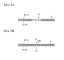
- FIG. 1A is a plan view of an antenna sheet 1 according to this embodiment, and FIG. 1B is a bottom view.
- the antenna sheet 1 includes a flexible substrate 2 formed from, for example, polyethylene naphthalate (PEN) or polyethylene terephthalate (PET).
- PEN polyethylene naphthalate
- PET polyethylene terephthalate
- the thickness of the substrate 2 is selected as appropriate within a range of, for example, approximately 0.02 mm to approximately 0.10 mm.
- An antenna circuit 3 is formed on a surface of the substrate 2.
- the antenna circuit 3 is made by performing etching and the like to pattern an aluminum thin film formed on the surface of the substrate 2, and is formed in a thin-film shape having a thickness of approximately 0.02 mm to 0.05 mm.
- the antenna circuit 3 includes an antenna coil 4 formed in a roughly rectangular spiral shape that corresponds to the shape of the substrate 2.
- An inside end of the antenna coil 4 expands in volume in a roughly circular shape, forming a terminal section 5. Bent portions (rectangle corners) of the antenna coil 4 are formed in roughly circular arc shapes.
- An outside end 6 of the antenna coil 4 is led toward one corner of the substrate 2.
- a roughly rectangular opening 7 is formed slightly to the antenna coil 4 side of one corner of the substrate 2.
- the opening 7 can store a part of an IC module explained later. While a storing section that can store a part of the IC module is here described as being the opening 7, this is not limitative of the invention.
- a recess can be provided as a storing section, with part of the IC module being accommodated in this recess. In comparison to using a recess, an opening obtains a deeper storing section with more space for storing the IC module, and can therefore increase the planarity of the antenna sheet 1.
- the outside end 6 of the antenna coil 4 that is led toward one corner of the substrate 2 is led toward one side 7a of the opening 7, and is connected to an antenna connecting land 8 (connecting section) which is formed along the side 7a.
- the antenna connecting land 8 is a roughly rectangular terminal section formed by increasing the width W1 of the antenna coil 4.
- An antenna connecting land 9 (connecting section) is formed on one side 7b opposing the side 7a of the opening 7 where the antenna connecting land 8 is formed.
- a wire 10 is one part of the antenna coil 4, and is connected to the antenna connecting land 9 formed opposing the antenna connecting land 8.
- the antenna connecting land 9 is formed in a roughly rectangular shape along the side 7b of the opening 7 by increasing the width W2 of the wire 10.
- One end of the wire 10 connects to the antenna connecting land 9, and another end side increases in volume in a roughly circular shape to form a terminal section 11.
- reinforcing patterns 12 and 13 (reinforcing sections) that reinforce the antenna connecting lands 8 and 9 are formed on a face on an opposite side to the face where the antenna circuit 3 is formed, in correspondence with the formation regions of the antenna connecting lands 8 and 9.
- the reinforcing patterns 12 and 13 are formed in rectangular shapes corresponding to the shapes of the antenna connecting lands 8 and 9 along the outlines of the antenna connecting lands 8 and 9 when viewed from above by, for example, etching and the like of a metal thin film as used for the antenna circuit 3, or by a similar method.
- connection section 8 By thus forming the reinforcing patterns 12 and 13 in correspondence with the formation regions of the connection section 8 on the face of an opposite side to the face where the antenna circuit 3 including the antenna connecting land 8 of the substrate 2 is formed, the connection section 8 can be supported by both the substrate 2 and the reinforcing patterns 12 and 13 formed on the rear side thereof, whereby the connection section 8 can be reinforced. This increases the flexural strength of the connection section 8, and can prevent breakage of the antenna coil 4 even when the section where a terminal section 25 of an IC module 20 and the connection section 8 of the antenna coil 4 are connected is subjected to repeated flexing.
- a jumper wire 14 is formed on a face on the opposite side to the face where the antenna circuit 3 of the substrate 2 is formed, and connects the terminal section 5 of the antenna coil 4 to the terminal section 11.
- the jumper wire 14 is formed using, for example, a similar method to that used for the antenna circuit 3. Both ends of the jumper wire 14 are increased in volume in a roughly circular shape to form terminal sections 15 and 16.
- the terminal sections 15 and 16 of the jumper wire 14 are provided in correspondence with the formation regions of the terminal section 5 and the terminal section 11 of the antenna coil 4 respectively.
- the terminal sections 15 and 16 of the jumper wire 14 and the terminal sections 5 and 11 of the antenna coil 4 are electrically connected together in conductive sections 17, which are formed in a plurality of point-like shapes in the formation regions of the terminal sections 15 and 16.
- the conduction section 17 is for example formed by a crimping process of applying pressure to the terminal section 15 (terminal section 16) of the jumper wire 14 and the terminal section 5 (terminal section 11) of the antenna coil 4 such as to pinch them from both sides, thereby breaking the substrate 2 and achieving physical contact between the terminal sections 5 and 15 (11 and 16).
- the conduction section 17 can be formed using a method other than the connection by the crimping process described above; as shown in FIG.
- a through hole 19A that penetrates the formation regions of the terminal sections 5 and 15 (11 and 16), fill the through hole 19A with a conductive paste 19 such as silver paste, and electrically connect the terminal section 15 (terminal section 16) of the jumper wire 14 to the terminal section 5 (terminal section 11) of the antenna coil 4.
- a conductive paste 19 such as silver paste
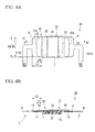
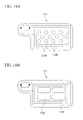
- FIG. 3A is a plan view of an IC module 20 according to this embodiment
- FIG. 3B is a cross-sectional view taken along the line A-A' of FIG. 3A
- the IC module 20 is formed from a lead frame 21, an IC chip 22 mounted on the lead frame 21, and a sealing resin section 23 that seals the IC chip 22.
- the lead frame 21 is formed roughly in the shape of a rectangle with its corners rounded to circular arc shapes when viewed from above.
- the lead frame 21 is formed from, for example, a copper-thread metal film and the like made by weaving copper thread into a film and silver plating this film.
- the lead frame 21 includes a die pad 24 that securely supports the IC chip 22, and an antenna land 25 (terminal section) that is connected to an input/output pad of the IC chip 22.
- the die pad 24 is slightly larger than the outer shape of the IC chip 22, and is fixed to the bottom of the IC chip 22.
- a gap S is provided between the die pad 24 and the antenna land 25, electrically insulating them from each other.
- the antenna land 25 is connected to the input/output pad of the IC chip 22 by bonding wires 26 of, for example, gold (Au). Since the antenna land 25 is used as a terminal section of the IC module 20 that is connected to an external circuit, it is formed extending along the long direction (length L direction) of the IC module 20.
- the sealing resin section 23 is formed roughly in the shape of a square with its corners rounded to circular arc shapes when viewed from above.
- the sealing resin section 23 is formed from, for example, a resin material such as epoxy resin, and covers the IC chip 22, the input/output pad of the IC chip 22, the bonding wires 26, the connection section between the antenna land 25 and the bonding wires 26, etc.
- the sealing resin section 23 is filled into the gap S between the die pad 24 and the antenna land 25, and extends across both of them.
- the thickness T1 of the IC module 20 is, for example, approximately 0.3 mm.
- the opening 7 of the antenna sheet 1 is opened in a roughly square shape corresponding to the sealing resin section 23, and slightly larger than the outer shape of the sealing resin section 23, enabling the opening 7 to store the roughly square-shaped sealing resin section 23 of the IC module 20.
- the width W3 of the pair of antenna connecting lands 8 and 9 provided opposing each other on both sides of the opening 7 of the antenna sheet 1 is roughly the same as, or slightly smaller than, the width W4 of the antenna land 25 of the IC module 20.
- the length L3 of the antenna connecting lands 8 and 9 of the antenna sheet 1 is larger than the length L4 of overlapping sections of the antenna land 25 of the IC module 20 and the antenna connecting lands 8 and 9.
- the length L3 of the antenna connecting lands 8 and 9 is roughly twice the length L4 of the overlapping sections of the antenna land 25 and the antenna connecting lands 8 and 9.
- the width W3 of the antenna connecting lands 8 and 9 of the antenna coil 4 connected to the antenna land 25 of the IC module 20 is made larger than the widths W1 and W2 of the antenna coil 4, so that it is roughly the same as, or slightly smaller than, the width W4 of the antenna land 25. This can disperse the stress in the width W3 direction, and prevent it from concentrating. Furthermore, the antenna connecting lands 8 and 9 can be connected along the entire width of the antenna land 25 in the width W4 direction, and the antenna connecting lands 8 and 9 can be reliably connected to the antenna land 25, enhancing the reliability of the antenna coil 4 and the inlet 30.
- the length L3 of the antenna connecting lands 8 and 9 of the antenna sheet 1 is made larger than the length L4 of the overlapping sections between the antenna land 25 of the IC module 20 and the antenna connecting lands 8 and 9. Furthermore, in this embodiment, the length L3 of the antenna connecting lands 8 and 9 is roughly twice as long as the length L4 of the overlapping sections between the antenna land 25 and the antenna connecting lands 8 and 9. As a result, edges 25e of the antenna land 25 are connected such as to be positioned roughly at the center of the insides of the ends of the antenna connecting lands 8 and 9 on the antenna coil 4 side. The edges 25e of the antenna land 25 consequently contact roughly with the centers of the antenna connecting lands 8 and 9 whose width W3 is made larger than the widths W1 and W2 of the antenna coil 4.
- the edges 25e of the antenna land 25 can be received roughly in the centers of the antenna connecting lands 8 and 9 whose width W3 is made larger. This can prevent concentration of stress in the antenna coil 4, and can thereby prevent breakage of the antenna coil 4.
- the substrate 2 functions as a reinforcing material for them. This prevents the antenna coil 4 with small widths W1 and W2 from making contact with the edges 25e of the antenna land 25, and can prevent breakage of the antenna coil 4.
- Reinforcing patterns 12 and 13 that reinforce the antenna connecting lands 8 and 9 are formed on a face of the substrate 2 that is on the opposite side to the face where the antenna circuit 3, in correspondence with the formation regions of the antenna connecting lands 8 and 9.
- the antenna connecting lands 8 and 9 are thus supported by both the substrate 2 and the reinforcing patterns 12 and 13 on its rear face, whereby the antenna connecting lands 8 and 9 can be reinforced.
- the flexural strength of the antenna connecting lands 8 and 9 is increased, and, when the sections where the antenna land 25 of the IC module 20 is connected to the antenna connecting lands 8 and 9 of the antenna coil 4 are subjected to repeated flexing, breakage of the antenna connecting lands 8 and 9, and breakage of the antenna coil 4, can be prevented.
- the reinforcing patterns 12 and 13 can be made to contact the antenna connecting lands 8 and 9, whereby they can assist the antenna connecting lands 8 and 9, and prevent the antenna coil 4 from breaking.
- the thin-film antenna coil 4 of this embodiment can be manufactured collectively by, for example, etching and the like, in comparison with a manufacturing process in which wire-wound antenna coils are individually wired, productivity of the antenna sheet 1 can be noticeably increased.
- the connection between the antenna land 25 and the antenna connecting lands 8 and 9 is accomplished by, for example, resistance welding or laser welding.
- a pair of welding electrodes 31 and 32 are separated and made to contact in the width W4 direction of the antenna land 25 of the IC module 20.
- a pressure of approximately 5N/mm 2 to 70N/mm 2 , and preferably approximately 40N/mm 2 is then applied from welding electrodes 31 and 32 between the antenna land 25 and the antenna connecting land 8. That is, a pressure of approximately 2.5N/mm 2 to 35N/mm 2 , and preferably approximately 20N/mm 2 , is applied from each of the welding electrodes 31 and 32.
- the coupling can be made more reliable by welding at multiple spots.
- a welding current I is fed from one welding electrode 31 to the other welding electrode 32.
- a voltage is applied between the welding electrodes 31 and 32 for a time of approximately 0.5 ms to 10.0 ms, such that the welding current I becomes, for example, approximately 300A to 600A. Consequently, current I supplied from the welding electrode 31 enters the antenna connecting land 8 from the antenna land 25, and enters the antenna land 25 from the antenna connecting land 8 at the point where the other welding electrode 32 makes contact. At this time, heat is generated at the interface between the antenna land 25 and the antenna connecting land 8 in the section where the welding electrodes 31 and 32 make contact.
- the antenna land 25 and the antenna connecting land 8 are welded and alloyed or thermally fused, thereby joining them together. Moreover, by reversing the direction of the welding current I, it is possible to achieve a well-balanced joint between the antenna land 25 and the antenna connecting land 8 at the sections where the welding electrodes 31 and 32 made contact. If the voltage, pressing force, and voltage application time are adjusted in the manner described above, the joining conditions can be optimized, enabling the antenna land 25 and the antenna connecting land 8 to be alloyed or thermally fused, and firmly joined together.
- the antenna connecting land 9 and the antenna land 25 are joined by welding, according to the same procedure as that of joining the antenna connecting land 8 and the antenna land 25.
- the pair of welding electrodes 31 and 32 in resistance welding, it is possible to arrange the pair of welding electrodes 31 and 32 in a separated manner in the length L direction of the IC module 20, make one of the welding electrodes 31 contact the antenna connecting land 8, and make the other welding electrode 32 contact on a point on the antenna land 25 where the antenna land 25 and the antenna connecting land 8 are joined.
- the antenna land 25 and the antenna connecting land 8 are pressured by applying a pressure of approximately 5N/mm 2 to 70N/mm 2 , preferably approximately 40N/mm 2 , to the welding electrode 32 provided on the antenna land 25.
- a welding current I is fed from one welding electrode 31 to the other welding electrode 32.
- the current, voltage, and application time of the welding current I are the same as in the resistance welding described in FIG. 5A .
- the current I supplied from the welding electrode 31 enters from the antenna connecting land 8, and enters the antenna land 25 from the antenna connecting land 8 at the point where the other welding electrode 32 makes contact.
- heat is generated at the interface between the antenna land 25 and the antenna connecting land 8 in the section where the other welding electrode 32 makes contact, whereby they are welded and alloyed or thermally fused, and joined.
- the contact resistance of the welded section on the antenna connecting land 8 side becomes relatively low. Consequently, the resistance heating of the welded section on the antenna connecting land 8 side can be relatively reduced in comparison with that on the antenna land 25, and the resistance heating welding energy on the antenna connecting land 8 side can be reduced. This can prevent the antenna connecting land 8, which has a welding temperature that is relatively low in comparison with the antenna land 25, from scattering during welding, and can achieve a stable joint, whereby the joining reliability and data carrier reliability can be increased.
- the welding electrodes 31 and 32 are then moved in the directions of the widths W3 and W4 of the antenna connecting land 8 and the antenna land 25, and a similar procedure is employed to join them by welding at a plurality of points in the directions of their widths W3 and W4.
- a similar procedure as that when joining the antenna connecting land 8 and the antenna land 25, the antenna connecting land 9 and the antenna land 25 are then joined by welding them at a plurality of points in the directions of their widths W3 and W4.
- the inlet 30 wherein the antenna land 25 of the IC module 20 and the antenna connecting lands 8 and 9 of the antenna sheet 1 are joined by welding at a plurality of points in the directions of the widths W3 and W4.
- the opening 7 that can store the sealing resin section 23 of the IC module 20 is formed in the antenna sheet 1, whereby the thickness of the sealing resin section 23 of the IC module 20 is absorbed into the opening 7 of the substrate 2, enabling the inlet 30 to be made thinner.
- the pair of welding electrodes 31 and 32 in separation on the antenna land 25 in the directions of the widths W3 and W4 direction, and welding the antenna land 25 to the antenna connecting lands 8 and 9 by resistance welding, a larger joining area can be achieved than when joining a conventional wire-wound antenna coil using ultrasound welding and the like. Also, by arranging the pair of welding electrodes 31 and 32 in separation in the length L direction of the IC module 20, only the other welding electrode 32 need be positioned on the antenna land 25. This enables the antenna land 25 to be made smaller.
- the antenna land 25 and the antenna connecting lands 8 and 9 can be fixed at a plurality of points. This can increase joining strength between the antenna land 25 of the IC module 20 and the antenna connecting lands 8 and 9 of the antenna sheet 1 with respect to flexing.
- the length L3 of the antenna connecting lands 8 and 9 is larger than the length of the antenna land 25 extending in the length L direction, the supporting area of the IC module 20 and the substrate 2 that is supported by the antenna connecting lands 8 and 9 can be increased. This increases durability against stress, and can prevent breakage of the antenna coil 4 even when flexing acts on the antenna connecting lands 8 and 9.
- the reinforcing patterns 12 and 13 are formed in formation regions of the antenna connecting lands 8 and 9 on a face of the substrate 2 of the antenna sheet 1 that is on the side opposite to the face where the antenna connecting lands 8 and 9 are formed. Consequently, heat during resistance welding can be transmitted to the reinforcing patterns 12 and 13, and released to the outside. This can prevent the substrate 2 from overheating and melting. Therefore, dirt can be prevented from sticking to the resistance welding apparatus and the product, and, in addition, decrease in the flexural strength of the antenna sheet 1 can be prevented.
- the inlet 30 includes the antenna sheet 1 described above, breakage of the antenna coil 4 due to the antenna sheet 1 can be prevented, increasing the reliability of data communications, and further increasing the productivity of the inlet 30. It is therefore possible to provide the inlet 30 that enables breakage of the antenna coil 4 to be prevented, has high data communications reliability, and high productivity.
- the antenna sheet 1 that prevents breakage of the antenna coil 4, increases reliability, and also increases productivity.
- the inlet 30 that enables breakage of the antenna coil 4 to be prevented, has increased reliability, and increased productivity.
- An antenna sheet 1A of this embodiment differs from the antenna sheet 1 described in the first embodiment in that slit holes 18 are formed in the antenna connecting lands 8 and 9. Since the other features are similar to those of the first embodiment, like reference numerals are appended to like parts, and these are not repetitiously explained.
- slit holes 18 are provided in the antenna connecting lands 8 and 9 of the antenna sheet 1A, and extend along the length L3 direction of the antenna connecting lands 8 and 9.
- a plurality of the slit holes 18 are formed in the width W3 direction of the antenna connecting lands 8 and 9.
- the slit holes 18 are formed such that, when the antenna connecting lands 8 and 9 are joined to the antenna land 25 of the IC module 20, the edges 25e of the antenna land 25 are in the middles of the slit holes 18.
- the joint section between the antenna connecting lands 8 and 9 and the antenna land 25 is subjected to flexing and the like, and cracks occur in the width W direction due to the edges 25e of the antenna land 25 making contact with the antenna connecting lands 8 and 9, when the cracks reach the slit holes 18, there is communication between the cracks traveling in the width W direction and the slit holes 18 extending in the length L3 direction, stopping the progression of the cracks in the width W direction.
- the cracks can be prevented from crossing the slit holes 18 and progressing in the width W direction of the antenna connecting lands 8 and 9, and breakage of the antenna coil 4 can be prevented. Furthermore, since a plurality of the slit holes 18 are formed in the width W direction of the antenna connecting lands 8 and 9, when a crack has progressed beyond an outer-side slit hole 18, another slit hole 18 adjacent thereto can prevent further progression of that crack.
- Antenna sheets 1B to 1D of this embodiment differ from the antenna sheet 1 described in the first embodiment in that through holes 19B to 19D are formed in the substrate 2. Since the other features are similar to those of the first embodiment, like reference numerals are appended to like parts, and these are not repetitiously explained.
- a roughly rectangular through hole 19B is formed in a region of the substrate 2 where the antenna coil 4 is not formed, and penetrates the substrate 2.
- a plurality of roughly rectangular through holes 19C are formed in the region of the substrate 2 where the antenna coil 4 is not formed, the substrate 2 being formed in a lattice shape.
- a plurality of roughly circular through holes 19D are formed in rows in the region of the substrate 2 where the antenna coil 4 is not formed.
- the through holes 19B to 19D are formed in this manner in the substrates 2 of the antenna sheets 1B to 1D, it becomes possible, when bonding base materials (explained later) to both sides of the antenna sheets 1B to 1D, to join the base materials via the through holes 19B to 19D. This can prevent peeling of the base materials from the antenna sheets 1B to 1D.
- the through holes 19B to 19D increase the flexibility of the antenna sheets 1B to 1D, make them lighter, and enable the quantity of material used for the substrate 2 to be reduced.
- an inlay 40 including the inlet 30 described in the above embodiment will be explained.
- an inlay 40 includes the inlet 30 described in the above embodiment, and a pair of base materials 41 and 42 that pinch the inlet 30.
- the inlay 40 is formed to a desired thickness T2 by pinching the inlet 30 between the base materials 41 and 42 and joining them into a single piece by lamination.
- an insulating plastic film PET-G: noncrystalline copolyester, PVC: vinyl chloride resin, etc.
- an insulating synthetic sheet Teslin ⁇ Registered trademark ⁇ , a polyolefin synthetic sheet manufactured by PPG Industries
- Yupo ⁇ Registered trademark ⁇ a polypropylene synthetic sheet manufactured by Yupo Corporation
- the inlay 40 includes the inlet 30 including the antenna sheet 1 described in the first embodiment, the antenna sheet 1 can prevent breakage of the antenna coil 4, the reliability of data communication can be increased, and productivity can be increased. Furthermore, the base materials 41 and 42 can reinforce the points of connection between the antenna connecting lands 8 and 9 of the antenna sheet 1 and the antenna land 25 of the IC module 20. It is therefore possible to provide the inlay 40 wherein breakage of the antenna coil 4 is prevented, and which achieves high reliable data communication, and high productivity.
- the base materials 41 and 42 can be joined together via the through holes 19B to 19D. This can increase the joint strength of the inlet 30 to the base materials 41 and 42, and prevent peeling of the base materials 41 and 42 from the inlet 30.
- the inlet 30 is broken by the peeling of the base materials 41 and 42. This can prevent unauthorized modification of the inlay 40.
- the flexibility of the inlay 40 can be increased, the inlay 40 can be made lighter, and the quantity of material used for the substrate 2 of the antenna sheet 1 can be reduced.
- the inlet 30 is pinched between the pair of base materials 41 and 42, and joined to them.
- the synthetic sheets mentioned above are used as the base materials 41 and 42
- the inlet 30 is joined to the base materials 41 and 42 using an adhesive laminating method of applying an adhesive to the antenna sheet 1, or to the faces of the base materials 41 and 42 that contact the antenna sheet 1, and joining them at a relatively low temperature of, for example, approximately 70°C to 140°C.
- EVA ethylene vinyl acetate resin
- EAA ethylene-acrylic acid copolymer resin
- polyester-based polyurethane-based
- polyurethane-based polyurethane-based
- an adhesive sheet that uses the resin used in the adhesives mentioned above can be pinched between the antenna sheet 1 and the base materials 41 and 42.
- the inlet 30 is joined to the base materials 41 and 42 using a thermal laminating method of melt-bonding them by applying pressure to them while heating them at a temperature that exceeds the softening temperature of the base materials 41 and 42, e.g. approximately 130°C to 170°C.
- the adhesive mentioned above can also be used when employing the thermal laminating method.
- the inlet 30 is joined to the base materials 41 and 42 to form a single piece, the outer shape of this single piece is shaped as desired.
- the inlay 40 shown in FIG. 8A and FIG. 8B can be manufactured.
- the softening temperature of the base materials 41 and 42 is approximately 100°C to 150°C for PET-G, and approximately 80°C to 100°C for PVC.
- the substrate 2 of the antenna sheet 1 is made from PEN or PET.
- the softening temperature of PEN is approximately 269°C
- the softening temperature of PET is approximately 258°C. That is, in comparison with a thermoplastic material having a low softening point such as PET-G, which was used for substrates in conventional antenna sheets, the heat-resistance temperature of the substrate 2 can be increased.
- the base materials 41 and 42 and the inlet 30 are heated to approximately 130°C to 170°C, the base materials 41 and 42 soften, whereas the substrate 2 of the antenna sheet 1 does not.
- the inlet 30 including the antenna sheet 1 and the base materials 41 and 42 are laminated and joined by thermal lamination, even if heat is applied to the substrate 2 of the antenna sheet 1, the substrate 2 can be prevented from plasticizing and flowing. Therefore, the antenna coil 4 can be prevented from moving in accordance with the flow of the substrate 2, and the reliability of data communication can be increased.
- the antenna coil 4 is formed in a film shape as described above, in comparison with a conventional wire-wound antenna coil, there is a larger contact area of the antenna coil 4 with the substrate 2, whereby the flow resistance of the antenna coil 4 can be increased. Therefore, it is possible to prevent the antenna coil 4 from moving according to the flow of the substrate 2, and to improve the reliability of data communication.
- aluminum thin films are collectively formed on a substrate sheet 50 with a plurality of formation regions for antenna sheets 1 arranged thereon in a matrix.
- the formed aluminum thin films are then collectively patterned, and an antenna circuit 3 is formed in each formation region 1a.
- jumper wires 14 and reinforcing patterns 12 and 13 are collectively formed in each formation region 1a on the rear face of the substrate sheet 50 in relation to the face where the antenna circuit 3 is formed.
- terminal sections 5 and terminal sections 11 of the antenna coil 4 of the antenna circuit 3 are collectively connected to terminal sections 15 and 16 of the jumper wires 14. Openings 7 for storing the sealing resin sections 23 of the IC modules 20 are collectively provided in the formation regions 1a.
- the antenna sheets 1 that were collectively formed in the plurality of formation regions 1a on the substrate sheet 50 are then cut and separated as individual antenna sheets 1. Thus a large quantity of the antenna sheets 1 can be collectively mass-produced, and productivity of manufacturing the antenna sheets 1 can be increased.
- the IC module 20 is mass-produced in parallel with the mass-production of the antenna sheets 1.
- lead frames 21 are collectively formed in formation regions 20a on a metal tape 60 where a plurality of formation regions 20a for IC modules 20 are arranged in a matrix.
- IC chips 22 are then collectively mounted on die pads 24 of the lead frames 21 in the formation regions 20a, and input/output pads of the IC chips 22 are collectively connected by bonding wires to the antenna lands 25 (see FIG. 3B ).
- Sealing resin sections 23 are formed collectively in each of the formation regions.
- the IC modules 20 collectively formed in the formation regions 20a of the metal tape 60 are then cut and separated as individual IC modules 20.
- each separated IC module 20 While the sealing resin section 23 of each separated IC module 20 is stored in the opening 7 of each separated antenna sheet 1, the antenna sheets 1 and the IC modules 20 are joined by resistance welding as described above. Thus, the inlets 30 can be collectively mass-produced, and their manufacturing productivity can be increased.
- a plurality of formation regions 40a for inlays 40 are provided on a first base-material sheet 71 and on a second base-material sheet 72.
- Inlets 30 are provided in each of the formation regions 40a of the first base-material sheet 71.
- the second base-material sheet 72 is then arranged on the inlets 30 such that the formation regions 40a of the first base-material sheet 71 and the formation regions 40a of the second base-material sheet 72 overlap.
- the base-material sheets 71 and 72 are joined to the inlet 30 using a joining method that is suitable for the material quality of the base-material sheet 71.
- the inlays 40 formed collectively in the formation regions 40a are then cut as required, with a plurality of inlays 40 linked together or with separated individual inlays 40. In this manner, the inlays 40 can be collectively mass-produced, and their manufacturing productivity can be increased.
- an electronic passport 100 will be explained as one example of a data carrier with non-contact type IC.
- an electronic passport 100 includes the inlay 40 described above as its front cover.
- a cover material 43 is joined to one face of the inlay 40 and becomes the front cover of the electronic passport 100.
- the cover material 43 is joined to the inlay 40 in this manner, the external appearance and texture of the wire 10 including the inlay 40 can be made similar to a conventional passport. Also, since the inlay 40 includes the antenna sheet 1 described above, it is possible to provide the electronic passport 100 wherein breakage of the antenna coil 4 can be prevented, and which has high reliability of data communication and high productivity.
- the present invention is not limited to the embodiment described above.
- the shape of the antenna coil need not be rectangular.
- the number of winds of the antenna coil 4 is also not limited to the embodiment described above.
- the material quality of the antenna circuit it can be made from a material other than aluminum, such as, for example, gold, silver, or copper. Since the terminal section 25 of the IC module 20 is often made from copper, when the antenna coil 4 is formed from copper, the connection section 8 of the antenna coil 4 and the terminal section 25 of the IC module 20 can be formed from the same metal, increasing the joint performance between the connection section 8 and the terminal section 25.
- perforations M can be formed in the antenna sheet 1. After the inlet has been pinched between the base materials and joined to them, when the base materials are attempted to be peeled from the inlet, stress concentrates in the perforations M in the antenna sheet 1, whereby the antenna sheet 1 is cut along the perforations M, and the antenna sheet 1 breaks. Therefore, unauthorized modification of the data carrier with non-contact type IC can be prevented.
- the adhesive can be applied in a predetermined pattern, such that the joint strength of the inlet and the base materials is made non-uniform. Consequently, when the base materials are attempted to be peeled from the inlet, a non-uniform stress acts on the antenna sheet, cutting and breaking the antenna sheet. Therefore, unauthorized modification of the data carrier with non-contact type IC can be prevented.
- the slit holes which extend in the length direction of the antenna connecting land, in only one point in the width direction. This can increase the connection area between the antenna connecting land and the antenna land.
- the opening in the substrate of the antenna sheet need not be formed. Furthermore, the position of the opening is not limited to that described in the embodiment.
- the opening can be formed along one side of the substrate.
- the entire IC module can be stored in the opening.
- the shape of the opening can be formed freely in accordance with the shape of the IC module to be stored in it.
- Base material openings for storing at least a part of the IC module can be formed in the base materials that pinch the inlet, at roughly the same position as the opening in the antenna sheet. Consequently, when pinching the inlet between the base materials, at least a part of the IC module can be stored in the base material openings, whereby the thickness of that section can be absorbed by the base materials, and the inlay can be made thin.
- a storing section an opening or a recess
- the antenna land 25 can be stored in this storing section.
- a storing section (an opening or a recess) having roughly the same shape as the sealing resin of the IC chip 22 when viewed from above can be provided in the base material to be attached to the opposite side to the antenna land 25 side, and the sealing resin of the IC chip 22 can be stored in this storing section.
- the joint section between the antenna connecting land and the antenna land of the module, which are joined by resistance welding, can be covered with epoxy resin, urethane resin, and the like. This can increase the reliability, vibration resistance, impact resistance, abrasion resistance, and the like, of the joint section.
- the embodiment describes an electronic passport as an example of a data carrier with non-contact type IC including an inlay
- the inlay of the present invention can also be used in, for example, electronic identification documents and various types of electronically confirmable activity history documents.
- the antenna sheet including the inlet can prevent breakage of the antenna coil of the commuter pass with an IC, the electronic money card, and the like, increasing the reliability of data communication and increasing productivity.
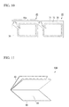
- FIG. 13 is a perspective view of a booklet 101 including an information medium 110 of this embodiment.
- the information medium 110 is affixed while being pinched between one of two cover members 102, which constitute a front cover and a rear cover of the booklet 101, and an inner bonding sheet 103 that is bonded to that cover member 102.
- a plurality of text sheets 104 are bound between the front cover and the rear cover, enabling the booklet 101 to be used for various purposes such as a savings passbook.
- the information medium 110 can be attached to face of one of the cover members 102 of the booklet 101.
- the information medium 110 is preferably attached to the inner face of the cover member 102 (the face where the cover members 102 touches the text sheets 104), rather than to its outer face.
- This configuration can protect the information medium 110 from external collisions against the booklet 101.
- the information medium 110 can be attached to one of the pages of the text sheets 104 of the booklet 101.
- a predetermined page of the text sheets 104 is given a larger area than the other pages, and folded such that its area becomes the same as the other pages, enabling the information medium 110 to be stored in a space formed by the folded section.
- the folded section is sealed by a method such as gluing or stitching.
- FIG. 14 is a view showing a mold of an IC inlet 111 that constitutes a part of the information medium 110.
- the IC inlet 111 includes an insulating sheet 112, an antenna coil 113 formed on both sides of the sheet 112, and an IC chip 114 attached to the sheet 112.
- the antenna coil 113 is formed by a method such as etching, wire bonding, or printing, using a conductor such as aluminum or silver. Of these, aluminum is inexpensive, making it preferable when considering the manufacturing cost.
- the antenna coil 113 includes an antenna loop 113A provided on one face of the antenna coil 113, and a jumper wire 113B provided on another face. The end of the jumper wire 113B is electrically connected to the antenna loop 113A via a through hole (not shown) provided in the sheet, or by a method such as crimping.
- the IC chip 114 is electrically connected to the antenna coil 113 by welding or the like, and attached to the sheet 112. This enables the IC inlet 111 to transmit and receive data to/from an external data reading device and such like in a non-contact manner.
- FIG. 15 is a cross-sectional view of an information medium 110 attached to a booklet 101.
- the information medium 110 is formed by using two sheet-like porous base materials 115 to pinch an IC inlet 111 from above and below.
- the IC inlet 111 and the porous base materials 115 are joined in a single piece by an adhesive 116.
- the porous base materials 115 should preferably have thermoplasticity.
- a base material can be obtained using a resin such as polyethylene, polypropylene, polyvinyl chloride, polyvinylidene chloride, polystyrene, polyvinyl acetate, polyester, or a combination of such resins, which is then subjected to a process such as mixing with porous particles such as silica, foaming by the addition of air during kneading, and stretching followed by punching. Since this type of base material is commercially available as resin sheet and synthetic paper in which print suitability is given to an inkjet, an offset, and the like, these can be used.
- the adhesive 116 is preferably hot-melting.
- adhesives made from various types of thermoplastic resin such as an ethylene-vinyl acetate copolymer (EVA)-based, ethylene-acrylic acid copolymer (EAA)-based, ethylene methyl acrylic acid copolymer (EMAA)-based, polyester-based, polyamide-based, polyurethane-based, and olefin-based, can suitably be used.
- a substance that is resistant to chloride ions is mixed into the adhesive 116, and prevents the permeation of chloride ions. That is, the layer that includes the adhesive 116 also functions as a chloride ion-resistant layer, which covers the antenna coil 113 formed on the IC inlet 111 and prevents the chloride ions from contacting the antenna coil 113, thereby preventing deterioration such as corrosion.
- Such an adhesive 116 can easily be obtained by adding an epoxy-based cross-linking agent to an EAA-based aqueous emulsion adhesive, or by using a gravure coater to apply an acrylic emulsion adhesive and the like according to a predetermined coating thickness, etc.
- an IC inlet having an aluminum antenna coil was pinched and affixed onto a sheet made from PET.
- the adhesive three types of conventional adhesives were used: an EMAA-based adhesive, an EMAA-based adhesive containing an epoxy-based cross-linking agent, and an acrylic-based adhesive 116; the coating thicknesses and additive quantities were varied. These samples were used in a salt water spray test described below. Samples were also created in which each of the adhesives complying with these conditions was applied directly to the IC inlet without pinching it between porous base materials, and these samples were used in a hydrochloride test described below.
- a salt water spray test was conducted in compliance with ISO 10373-1, and the results were evaluated in the following three stages. A: No corrosion whatsoever, B: Partial corrosion, C: Total corrosion and defective performance.
- Test 1 and Test 2 indicated a consistently good correlation.
- the samples that were joined using only an EMAA-based thermoplastic adhesive in the conventional manner could not obtain sufficient durability against the salt water spray, even when the thickness of the adhesive coating was increased.
- the adhesive becomes resistant to chloride ions.
- Durability was enhanced by increasing the mixture ratio of the epoxy-based cross-linking agent.
- the acrylic-based adhesives had greater durability against salt water spray than the EMAA-based adhesives, and were resistant to chloride ions. Their chloride ion resistance was increased by making the coating thicker.
- an antenna coil 113 is made by providing an antenna loop 113A and a jumper wire 113B on a sheet 112.
- An IC chip 114 is connected the antenna coil 113 to form an IC inlet 111.
- the method is similar to a conventional method for manufacturing an IC inlet.
- the periphery of the sheet 112 is cut away; in addition, a region of the sheet 112 that is inside the antenna loop 113A is removed, forming a through hole 112A which penetrates in the thickness direction of the sheet 112.
- the through hole 112A can be suitably formed using a punching mold. Therefore, even in cases such as when IC inlets are mass-produced by forming a great many antenna coils on a single large sheet, punching enables a great many through holes to be easily made.
- the size of the through hole 112A is preferably set such that the area of a cross-section orthogonally intersecting the thickness direction of the through hole 112A occupies 60% or more of the region enclosed within the innermost antenna of the antenna loop 113A.
- the area of the sheet 112 is preferably set at not less than 3% and less than 20% of the area of the porous base material 115 it is joined to.
- each of the two porous base materials 115 formed with a desired size is coated with an adhesive 116 which has been made resistant to chloride ions in the manner described above.
- the faces coated with the adhesive 116 are arranged opposite the IC inlet 111, which is then pinched and pressed by the porous base materials 115 from above and below. In this manner, a chloride ion-resistant layer including the adhesive 116 is formed such as to cover the antenna coil 113.
- porous base materials 115 are made from thermoplastic resin, if heat is applied at the same time as applying pressure, the porous base materials 115 soften and deform, whereby projections and recesses on the surface of the IC inlet 111 due to the IC chip 114 and the like are absorbed by the porous base materials 115. As a result, an information medium 110 having flat top and bottom faces can be obtained.
- a conventional method of manufacturing an IC card and the like can be used in the above process, which can be executed using, for example, a hot press.
- the information medium 110 thus obtained is pinched between the front cover member 102 and the inner bonding sheet 103, and, when these are all joined in a single piece using an adhesive (not shown), the booklet 101 including the information medium 110 can be obtained.
- the porous base materials 115 that constitute the outer faces of the information medium 110 have good close attachment to various types of adhesive, and can therefore be excellently joined without problems, even when using a water-based emulsion adhesive and the like used in conventional booklet joining.
- the outer faces of the information medium 110 are flatly formed without projections and recesses, the information medium 110 can be attached without spoiling the external appearance of the booklet 101.
- a reaction curing type adhesive with no volume change When joining the cover members 102 to the information medium 110, it is preferable to use a reaction curing type adhesive with no volume change.
- a dry curing type adhesive with volume change if a part of the information medium includes projections and recesses, the quantity of adhesive used will increase in the recesses. As a result, there is greater volume reduction when drying, and there are cases where the external appearance is spoiled due to a partial collapse of cover members 102 and the like which overlap the recesses.
- the adhesive with no volume change it is possible to use, for example, a two-part mixed type epoxy-based adhesive, a moisture curing type silicon-based adhesive, a one-part curing type urethane-based adhesive, and the like.
- hot-melt adhesive can also be used, such as EVA-based, EAA-based, polyester-based, polyamide-based, polyurethane-based, and olefin-based.
- EVA-based EAA-based
- polyester-based polyamide-based
- polyurethane-based polyurethane-based
- olefin-based a reactive type hot-melt adhesive is more preferable.
- a PET sheet having a thickness of 38 micrometers ( ⁇ m) was used as the sheet 112.
- Aluminum deposition and printing of a mask layer having the same shape as the antenna coil 113 were performed on both faces of the sheet 112, and pattern etching was used to form an antenna loop 113A on one face and a jumper wire 113B on the other face.
- the antenna loop 113A and the jumper wire 113B were joined by caulking, and an IC chip 114 was welded to the connection terminal section of the antenna coil 113.
- FIG. 17 shows dimensions of each section of an information medium 110A in this test.
- the outer periphery of the roughly square antenna loop 113A is 80 millimeters (mm) x 48 mm, and its inner periphery is 67 mm x 37 mm. Subsequently, a part of the sheet 112 that is inside the antenna loop 113A was punched away to form a through hole 112A having a roughly square shape of 65 mm x 35 mm. Moreover, leaving an outline that is 2 mm from the outer periphery of the antenna loop 113A and the IC chip 114, the sheet 112 that was further to the outside than that was removed by punching. The cross-sectional area orthogonal to the thickness direction of the through hole 112A thereby becomes approximately 91% of the region inside the periphery of the antenna loop 113A. In this manner the IC inlet 111 was produced.
- a Teslin sheet (a product manufactured by PPG Industries; thickness: 380 ⁇ m) was used as the material for the porous base materials 115.
- An adhesive obtained by mixing 1 part by weight of a soluble epoxy curing agent with 20 parts by weight of an EMAA-based aqueous emulsion adhesive (AC-3100, a product manufactured by Chuo Rika Kogyo Corporation), was applied to one face of each sheet at an amount of 5g/m 2 (coating thickness: approximately 5 ⁇ m). After drying, two sheets of 150 mm x 200 mm were cut, obtaining porous base materials 115. At this point in time, the area of the IC inlet 111 was 15% of the area of the porous base materials 115. A hole corresponding in size to the lead frame of the IC chip 114 was then drilled into one of the porous base materials 115, and a hole corresponding in size to the mold of the IC chip 114 was drilled into the other porous base material 115.
- the IC inlet 111 and the porous base materials 115 were arranged such that the read frame and mold of the IC chip 114 were stored in the holes formed in the respective porous base materials 115.
- the IC inlet 111 was then laminated by pinching it from above and below by the porous base materials 115, and temporarily held by spot heating.
- the porous base materials 115 and the IC inlet 111 that were temporarily held by spot heating were pinched between two stainless steel plates and subjected to heating and pressurizing to join them completely together, thereby obtaining the information medium 110A.
- the heating and pressurizing conditions were adjusted as appropriate between a heater unit temperature of 100°C to 160°C, pressure of 5 KgF/cm 2 to 30 KgF/cm 2 , and a processing time of 15 seconds to 120 seconds.
- a cloth for book cover (Enviromate H, a product manufactured by ICG Holliston) was used as the material for the cover members 102. This was cut to the same size as the information medium 110A to obtain the cover members 102.
- a moisture curing hot-melt adhesive (Esdain 9635, a product manufactured by Sekisui Fuller Corp.) was melted with a heat roll coater, and an amount of 20 g/m 2 was applied to the cover members.
- the outer faces of the porous base materials 115 of the information medium 110A were affixed to the cover members 102 coated with the hot-melt adhesive, pressurized with rollers, and thereafter subjected to an aging process.
- a plurality of text sheets 104 and one inner bonding sheet 103 are collated, and their centers are stitched using a sewing machine, thereby manufacturing a text section with the inner bonding sheet 103 attached to an outermost section.
- a water-based emulsion adhesive (SP-2850, a product manufactured by Konishi Corp.) was then applied at an amount of 20g/m 2 to the porous base materials 115 on the opposite side of the information medium 110A to the side affixed to the cover members 102, and the porous base materials 115 were affixed to the inner bonding sheet 103.
- the book thus obtained is opened and cut to 125 mm x 180 mm, obtaining a booklet 101. That is, the dimensions of the porous base materials 115 shown in FIG. 17 are the dimensions when the booklet 101A is folded.
- the IC inlet 111 was made using the same method as in the example, the size of the through hole 112A was 40 mm x 30 mm. The cross-sectional area orthogonal to the thickness direction of the through hole 112A was approximately 48% of the region inside the periphery of the antenna loop 113A. Moreover, the IC inlet 111 was attached to a booklet using the same procedure as the example, to obtain a booklet having roughly the same external appearance.
- the front and rear covers of the booklet 101A of the example manufactured in the manner described above are formed smoothly, no projections or recesses being generated by the attachment of the information medium 110A. Furthermore, in various durability evaluation experiments, including storing it in a high temperature and high moisture environment and subjecting it to a bend test, the IC inlet 111 suffered no deterioration, especially of the antenna coil 113, and thus achieved excellent results.
- the information medium 110 of this embodiment when the IC inlet 111 is pinched between the porous base materials 115, which have been coated with the chloride ion-resistant adhesive 116, and joined to them in a single piece, a chloride ion-resistant layer is formed such as to cover the antenna coil 113 including the antenna loop 113A and the jumper wire 113B. Therefore, even when the information medium 110 is attached to a booklet, chloride ions that permeate the cover members 102 and the inner bonding sheet 103 are prevented from reaching the antenna coil 113 and acting upon it, whereby deterioration of the antenna coil 113 is excellently prevented. Therefore, even when the information medium is applied in a booklet, a configuration can be accomplished where the information medium functions with high reliability for a long time period.
- the IC inlet 111 is pinched from above and below by the porous base materials 115, projections and recesses due to the IC chip 114 and the like are absorbed by the porous base materials 115, whereby the information medium can be configured with smooth top and bottom faces. As a result, even when the information medium 110 is applied in a booklet, the external appearance is not spoiled.
- the through hole 112A is provided in the sheet 112 of the IC inlet 111, at the point of the through hole 112A, the porous base materials 115 are firmly affixed by the adhesive 116 without the sheet 112 in between them. Therefore, the entire information medium 110 can be stably joined. In addition, it is difficult to remove only the IC inlet for purposes of counterfeiting and such like, whereby security can be increased.
- the chloride ion-resistant layer can instead be formed using a chloride ion-resistant substance other than the adhesive 116, such as, for example, an epoxy-based resin.
- the chloride ion-resistant layer can be formed on the IC inlet 111 by a method such as coating, or it can be formed on the faces of the porous base materials 115 that will be joined to the IC inlet 111.
- a chloride ion-resistant layer and an adhesive can be formed on the surfaces of the porous base materials using a printing device and the like that is capable of multi-color printing, enabling the two layers to be formed efficiently without greatly modifying the process.
- the through hole formed in the sheet 112 is not limited to the single hole described in the embodiments.
- a plurality of through holes 112B and 112C can be provided, as in the modifications shown in FIG. 18A and FIG. 18B .
- This configuration achieves a plurality of dispersed points where the porous base materials are firmly joined together, obtaining a highly secure information medium which is more difficult to peel off.
- each of the embodiments describes an example of an information medium wherein an IC inlet is pinched between porous base materials
- the information medium can be configured without providing porous base materials, and with a chloride ion-resistant layer formed directly on the IC inlet. While such an information medium is slightly less smooth than one that includes porous base materials, it can be applied in a booklet by appropriately selecting an adhesive for joining it to the front cover member and the inner bonding sheet. It then becomes possible to suppress deterioration of the antenna coil and ensure the functions of the information medium, while using the booklet over a long time period.
- the fourth embodiment described above can be applied in any one of the first to the third embodiments.
- the antenna coil 4 of the first to the third embodiments can be covered with the adhesive 116 that forms the chloride ion-resistant layer of the fourth embodiment.
- an adhesive that is not resistant to chloride ions can be applied to the antenna coil 4, and this adhesive can then be covered with a chloride ion-resistant layer.
- sheet-like porous base materials 115 that pinch the antenna coil 113 such as to cover it can be provided on the entirety of both faces of the sheet 112, and the adhesive 116 which constitutes a chloride ion-resistant layer can be formed on faces of the porous base materials 115 that oppose the sheet 112.
- both faces of the non-contact type information medium 110 can be made flat, and, when the information medium 110 is attached to a booklet, projections and recesses are less likely to be generated on the page it is attached to.
- the porous base materials 115 are affixed by the adhesive 116 to the sheet 112
- the adhesive 116 since the adhesive 116 is resistant to chloride ions, it functions as a chloride ion-resistant layer. This makes it possible to form the chloride ion-resistant layer at the same time as affixing the porous base materials, thereby increasing the manufacturing efficiency.
- the sheet 112 includes a through hole 112A penetrating the thickness direction of the sheet 112, and the porous base materials 115 are joined at the through hole 112A without the sheet 112 in between, whereby the porous base materials 115 are joined together directly at the through hole. Therefore, the porous base materials 115 can be joined more firmly, and security can be increased.
- the cross-sectional area in the direction that orthogonally intersects the axis line of the through hole 112A is given a value of not less than 60% of the area of the region inside the loop of the antenna coil 113; also, the area of the sheet 112 at the time of joining it to the porous base materials 115 is not less than 3% and less than 20% of the area of the porous base materials 115, whereby the porous base materials 115 can be more firmly joined.
- the antenna coil 113 since the antenna coil 113 includes aluminum, it can be formed inexpensively and reliably.
- the antenna coil 113 of the non-contact type information medium 110 attached to the booklet 101 is less likely to deteriorate, and can be used stably for a long period of time.
- the fourth embodiment describes a case where the adhesive 116 constituting a chloride ion-resistant layer is formed such as to cover the antenna coil 113, this is not limitative of the invention.
- a water-resistant layer can be formed such as to cover the antenna coil 113.
- rubber latex such as natural rubber latex and styrene butadiene copolymer latex, vinyl chloride-vinyl acetate-based resin, polyester-based resin, polyurethane-based resin, a (meta)acrylic-based resin such as (meta)acrylate-styrene acid/alkyl ester, (meta)acrylic acid/alkyl ester copolymer, or an epoxy-based resin, etc.
- the present invention can be applied in an antenna sheet, a transponder, a booklet, and the like, which can make the product thin.
Priority Applications (3)
| Application Number | Priority Date | Filing Date | Title |
|---|---|---|---|
| PL08830775T PL2192530T3 (pl) | 2007-09-14 | 2008-09-12 | Folia antenowa, transponder i książka |
| PL13155292T PL2602747T3 (pl) | 2007-09-14 | 2008-09-12 | Folia antenowa, transponder, i książka |
| EP13155292.9A EP2602747B1 (de) | 2007-09-14 | 2008-09-12 | Antennenfolie, Transponder und Broschüre |
Applications Claiming Priority (3)
| Application Number | Priority Date | Filing Date | Title |
|---|---|---|---|
| JP2007239982 | 2007-09-14 | ||
| JP2008187007 | 2008-07-18 | ||
| PCT/JP2008/066570 WO2009035094A1 (ja) | 2007-09-14 | 2008-09-12 | アンテナシート、トランスポンダ及び冊子体 |
Related Child Applications (2)
| Application Number | Title | Priority Date | Filing Date |
|---|---|---|---|
| EP13155292.9A Division EP2602747B1 (de) | 2007-09-14 | 2008-09-12 | Antennenfolie, Transponder und Broschüre |
| EP13155292.9 Division-Into | 2013-02-14 |
Publications (3)
| Publication Number | Publication Date |
|---|---|
| EP2192530A1 true EP2192530A1 (de) | 2010-06-02 |
| EP2192530A4 EP2192530A4 (de) | 2010-10-27 |
| EP2192530B1 EP2192530B1 (de) | 2013-03-27 |
Family
ID=40452100
Family Applications (2)
| Application Number | Title | Priority Date | Filing Date |
|---|---|---|---|
| EP08830775A Active EP2192530B1 (de) | 2007-09-14 | 2008-09-12 | Antennenfolie, transponder und buch |
| EP13155292.9A Active EP2602747B1 (de) | 2007-09-14 | 2008-09-12 | Antennenfolie, Transponder und Broschüre |
Family Applications After (1)
| Application Number | Title | Priority Date | Filing Date |
|---|---|---|---|
| EP13155292.9A Active EP2602747B1 (de) | 2007-09-14 | 2008-09-12 | Antennenfolie, Transponder und Broschüre |
Country Status (15)
| Country | Link |
|---|---|
| US (1) | US8519905B2 (de) |
| EP (2) | EP2192530B1 (de) |
| JP (1) | JP5370154B2 (de) |
| KR (2) | KR101163300B1 (de) |
| CN (1) | CN101836225B (de) |
| AU (1) | AU2008297839B2 (de) |
| BR (1) | BRPI0817336A2 (de) |
| CA (1) | CA2699552C (de) |
| ES (2) | ES2563451T3 (de) |
| MX (1) | MX2010002872A (de) |
| MY (1) | MY159909A (de) |
| PL (2) | PL2192530T3 (de) |
| RU (1) | RU2471232C2 (de) |
| TW (1) | TWI379241B (de) |
| WO (1) | WO2009035094A1 (de) |
Cited By (4)
| Publication number | Priority date | Publication date | Assignee | Title |
|---|---|---|---|---|
| US8232630B2 (en) | 2009-08-26 | 2012-07-31 | Toppan Printing Co., Ltd. | Contactless communication medium |
| EP2426626A4 (de) * | 2009-04-28 | 2012-12-05 | Toppan Printing Co Ltd | Antennenfolie, datenträger mit kontaktfreier integrierter schaltung und verfahren zur herstellung für eine antennenfolie |
| FR3013152A1 (fr) * | 2013-11-14 | 2015-05-15 | Smart Packaging Solutions | Antenne double face pour carte a puce |
| EP3985797A4 (de) * | 2019-06-13 | 2023-11-15 | Passcon Co., Ltd | Sende- und empfangsantenne für drahtlose aufladung sowie vorrichtung und verfahren zu deren herstellung |
Families Citing this family (31)
| Publication number | Priority date | Publication date | Assignee | Title |
|---|---|---|---|---|
| EP2256672B1 (de) * | 2008-02-22 | 2016-04-13 | Toppan Printing Co., Ltd. | Transponder und buchform |
| JP2010257416A (ja) * | 2009-04-28 | 2010-11-11 | Toppan Printing Co Ltd | 情報記録媒体、非接触型ic付データキャリア、および情報記録媒体の製造方法 |
| DE102009023715A1 (de) * | 2009-06-03 | 2010-12-09 | Leonhard Kurz Stiftung & Co. Kg | Sicherheitsdokument |
| JP5428761B2 (ja) * | 2009-10-30 | 2014-02-26 | 凸版印刷株式会社 | アンテナシート、トランスポンダ及び冊子体 |
| JP5397193B2 (ja) * | 2009-11-30 | 2014-01-22 | 凸版印刷株式会社 | 非接触型情報媒体と非接触型情報媒体付属冊子 |
| JP2011237969A (ja) * | 2010-05-10 | 2011-11-24 | Toppan Printing Co Ltd | 非接触型情報媒体及びこれを内蔵した冊子 |
| JP2012037957A (ja) * | 2010-08-04 | 2012-02-23 | Nippon Signal Co Ltd:The | リーダライタ及びドア開閉装置 |
| JP2012073725A (ja) * | 2010-09-28 | 2012-04-12 | Toppan Printing Co Ltd | 非接触通信媒体、冊子及びその製造方法 |
| EP2461275A1 (de) * | 2010-12-02 | 2012-06-06 | Gemalto SA | Sicherheitsdokument und Verfahren zur Herstellung von Sicherheitsdokumenten |
| JP2012160108A (ja) * | 2011-02-02 | 2012-08-23 | Toppan Printing Co Ltd | 非接触型情報記録媒体 |
| JP5834585B2 (ja) * | 2011-07-25 | 2015-12-24 | 凸版印刷株式会社 | 非接触通信媒体及びその製造方法 |
| TWI453677B (zh) * | 2011-12-01 | 2014-09-21 | Mutual Pak Technology Co Ltd | 射頻識別標籤與具有其之衣物 |
| US8763914B2 (en) * | 2012-01-17 | 2014-07-01 | On Track Innovations Ltd. | Decoupled contactless bi-directional systems and methods |
| WO2013161781A1 (ja) * | 2012-04-24 | 2013-10-31 | 凸版印刷株式会社 | 非接触型情報媒体及び非接触型情報媒体付属冊子 |
| WO2014045518A1 (ja) * | 2012-09-18 | 2014-03-27 | パナソニック株式会社 | アンテナ、送信装置、受信装置、三次元集積回路、及び非接触通信システム |
| FR3001070B1 (fr) * | 2013-01-17 | 2016-05-06 | Inside Secure | Systeme d'antenne pour microcircuit sans contact |
| US10909440B2 (en) * | 2013-08-22 | 2021-02-02 | Texas Instruments Incorporated | RFID tag with integrated antenna |
| WO2015085064A1 (en) * | 2013-12-05 | 2015-06-11 | Uniqarta, Inc. | Electronic device incorporated into a sheet |
| US11514288B2 (en) * | 2014-08-10 | 2022-11-29 | Amatech Group Limited | Contactless metal card constructions |
| US11618191B2 (en) | 2016-07-27 | 2023-04-04 | Composecure, Llc | DI metal transaction devices and processes for the manufacture thereof |
| US10762412B2 (en) | 2018-01-30 | 2020-09-01 | Composecure, Llc | DI capacitive embedded metal card |
| CN109564634A (zh) | 2016-07-27 | 2019-04-02 | 安全创造有限责任公司 | 用于交易卡的经包覆模制的电子部件及其制造方法 |
| US10977540B2 (en) | 2016-07-27 | 2021-04-13 | Composecure, Llc | RFID device |
| CN106909962A (zh) * | 2017-02-08 | 2017-06-30 | 珠海恒冠宇科技有限公司 | 柔性接触式ic本证、读写机具及旧设备升级办法 |
| CN113346221B (zh) * | 2017-03-30 | 2024-03-19 | 住友电气工业株式会社 | 无线模块 |
| WO2019045638A1 (en) * | 2017-08-28 | 2019-03-07 | Smartflex Technology Pte Ltd | INTEGRATED CIRCUIT MODULES AND INTELLIGENT CARDS INCORPORATING THEM |
| PE20201177A1 (es) | 2017-09-07 | 2020-11-03 | Composecure Llc | Tarjeta de transaccion con componentes electronicos incorporados y procedimiento para su fabricacion |
| US11151437B2 (en) | 2017-09-07 | 2021-10-19 | Composecure, Llc | Metal, ceramic, or ceramic-coated transaction card with window or window pattern and optional backlighting |
| DK3698280T3 (da) | 2017-10-18 | 2022-10-31 | Composecure Llc | Metal-, keramik- eller keramikbelagt transaktionskort med vindue eller vinduesmønster og eventuelt baggrundsbelysning |
| USD948613S1 (en) | 2020-04-27 | 2022-04-12 | Composecure, Llc | Layer of a transaction card |
| JP7095825B1 (ja) | 2022-03-30 | 2022-07-05 | 豊田合成株式会社 | 車両用外装部品 |
Citations (6)
| Publication number | Priority date | Publication date | Assignee | Title |
|---|---|---|---|---|
| US5708419A (en) * | 1996-07-22 | 1998-01-13 | Checkpoint Systems, Inc. | Method of wire bonding an integrated circuit to an ultraflexible substrate |
| US5852289A (en) * | 1994-09-22 | 1998-12-22 | Rohm Co., Ltd. | Non-contact type IC card and method of producing the same |
| US6233818B1 (en) * | 1996-02-12 | 2001-05-22 | David Finn | Method and device for bonding a wire conductor |
| US20020190132A1 (en) * | 2001-06-14 | 2002-12-19 | Georges Kayanakis | Contactless smart card with an antenna support and a chip support made of fibrous material |
| US20050046573A1 (en) * | 2001-04-30 | 2005-03-03 | Velasco Francisco Martinez De | Selective metal removal process for metallized retro-reflective and holographic films and radio frequency devices made therewith |
| US20080155822A1 (en) * | 2007-01-01 | 2008-07-03 | Advanced Microelectronic And Automation Technology Ltd. | Methods of connecting an antenna to a transponder chip |
Family Cites Families (25)
| Publication number | Priority date | Publication date | Assignee | Title |
|---|---|---|---|---|
| JPH09109577A (ja) * | 1995-10-13 | 1997-04-28 | Toppan Printing Co Ltd | 非接触記憶媒体を有するカードおよびその製造方法 |
| TW297501U (en) | 1996-06-22 | 1997-02-01 | yun-rong Xue | Finned-pipe type evaporating device utilizing hot air to defrost |
| US6157344A (en) * | 1999-02-05 | 2000-12-05 | Xertex Technologies, Inc. | Flat panel antenna |
| US6353420B1 (en) * | 1999-04-28 | 2002-03-05 | Amerasia International Technology, Inc. | Wireless article including a plural-turn loop antenna |
| JP2002042068A (ja) | 2000-07-21 | 2002-02-08 | Dainippon Printing Co Ltd | 非接触型データキャリア及び非接触型データキャリアを有する冊子 |
| JP2002109502A (ja) | 2000-07-28 | 2002-04-12 | Oji Paper Co Ltd | Ic実装体とその製造方法 |
| WO2003030300A1 (fr) * | 2001-09-28 | 2003-04-10 | Mitsubishi Materials Corporation | Bobine antenne et etiquette d'utilisation rfid l'utilisant, antenne d'utilisation de transpondeur |
| JP3881366B2 (ja) | 2002-12-06 | 2007-02-14 | 株式会社フジクラ | アンテナ |
| JP2004280503A (ja) | 2003-03-17 | 2004-10-07 | Toppan Printing Co Ltd | コンビネーションicカード |
| US7090606B2 (en) | 2003-07-03 | 2006-08-15 | The Gates Corporation | Adjustable tensioner |
| JP2005084757A (ja) | 2003-09-04 | 2005-03-31 | Seiko Epson Corp | 無線通信icデバイス付き名刺 |
| KR20060100199A (ko) | 2003-11-11 | 2006-09-20 | 토레 엔지니어링 가부시키가이샤 | 비접촉 아이디 카드 및 그의 제조 방법 |
| WO2005071608A1 (en) * | 2004-01-23 | 2005-08-04 | Semiconductor Energy Laboratory Co., Ltd. | Id label, id card, and id tag |
| US7083083B2 (en) * | 2004-04-27 | 2006-08-01 | Nagraid S.A. | Portable information carrier with transponders |
| US7546946B2 (en) * | 2004-06-29 | 2009-06-16 | Kanzaki Specialty Papers, Inc. | Multifunction, direct thermal recording material |
| JP2006155224A (ja) | 2004-11-29 | 2006-06-15 | Mitsubishi Polyester Film Copp | Rfidタグ用ポリエステルフィルム |
| JPWO2006077732A1 (ja) * | 2005-01-18 | 2008-06-19 | コニカミノルタエムジー株式会社 | 印刷版材料、製版方法、印刷方法、平版印刷版材料集合体用包装体、平版印刷版材料の集合体及び製版印刷方法 |
| FR2882174B1 (fr) * | 2005-02-11 | 2007-09-07 | Smart Packaging Solutions Sps | Procede de fabrication d'un dispositif microelectronique a fonctionnement sans contact notamment pour passeport electronique |
| RU2286600C1 (ru) * | 2005-05-18 | 2006-10-27 | Государственное образовательное учреждение высшего профессионального образования Московский государственный институт электронной техники (технический университет) | Электронный модуль бесконтактной индентификации |
| JP5352045B2 (ja) | 2005-06-03 | 2013-11-27 | 株式会社半導体エネルギー研究所 | 集積回路装置の作製方法 |
| US7545276B2 (en) * | 2005-09-13 | 2009-06-09 | Semiconductor Energy Laboratory Co., Ltd. | Semiconductor device |
| TW200713074A (en) | 2005-09-26 | 2007-04-01 | Ind Tech Res Inst | Flexible RFID label and manufacturing method thereof |
| TWI297501B (en) | 2006-03-17 | 2008-06-01 | Elite Semiconductor Esmt | Method and apparatus for determining sensing timing of flash memory |
| TWM305942U (en) | 2006-05-25 | 2007-02-01 | Sunbest Technology Co Ltd | Radio frequency identification clothing tag |
| JP4855880B2 (ja) * | 2006-09-20 | 2012-01-18 | リンテック株式会社 | アンテナ回路、アンテナ回路の製造方法、icインレット、icタグ |
-
2008
- 2008-09-12 PL PL08830775T patent/PL2192530T3/pl unknown
- 2008-09-12 CN CN2008801124273A patent/CN101836225B/zh not_active Expired - Fee Related
- 2008-09-12 EP EP08830775A patent/EP2192530B1/de active Active
- 2008-09-12 JP JP2009532247A patent/JP5370154B2/ja active Active
- 2008-09-12 ES ES13155292.9T patent/ES2563451T3/es active Active
- 2008-09-12 KR KR1020107006003A patent/KR101163300B1/ko active IP Right Grant
- 2008-09-12 MY MYPI2010001110A patent/MY159909A/en unknown
- 2008-09-12 PL PL13155292T patent/PL2602747T3/pl unknown
- 2008-09-12 MX MX2010002872A patent/MX2010002872A/es active IP Right Grant
- 2008-09-12 BR BRPI0817336-2A patent/BRPI0817336A2/pt not_active Application Discontinuation
- 2008-09-12 US US12/733,666 patent/US8519905B2/en active Active
- 2008-09-12 TW TW097134957A patent/TWI379241B/zh not_active IP Right Cessation
- 2008-09-12 AU AU2008297839A patent/AU2008297839B2/en active Active
- 2008-09-12 WO PCT/JP2008/066570 patent/WO2009035094A1/ja active Application Filing
- 2008-09-12 KR KR1020127006038A patent/KR101237107B1/ko active IP Right Grant
- 2008-09-12 CA CA2699552A patent/CA2699552C/en not_active Expired - Fee Related
- 2008-09-12 ES ES08830775T patent/ES2415364T3/es active Active
- 2008-09-12 EP EP13155292.9A patent/EP2602747B1/de active Active
- 2008-09-12 RU RU2010109058/08A patent/RU2471232C2/ru not_active IP Right Cessation
Patent Citations (6)
| Publication number | Priority date | Publication date | Assignee | Title |
|---|---|---|---|---|
| US5852289A (en) * | 1994-09-22 | 1998-12-22 | Rohm Co., Ltd. | Non-contact type IC card and method of producing the same |
| US6233818B1 (en) * | 1996-02-12 | 2001-05-22 | David Finn | Method and device for bonding a wire conductor |
| US5708419A (en) * | 1996-07-22 | 1998-01-13 | Checkpoint Systems, Inc. | Method of wire bonding an integrated circuit to an ultraflexible substrate |
| US20050046573A1 (en) * | 2001-04-30 | 2005-03-03 | Velasco Francisco Martinez De | Selective metal removal process for metallized retro-reflective and holographic films and radio frequency devices made therewith |
| US20020190132A1 (en) * | 2001-06-14 | 2002-12-19 | Georges Kayanakis | Contactless smart card with an antenna support and a chip support made of fibrous material |
| US20080155822A1 (en) * | 2007-01-01 | 2008-07-03 | Advanced Microelectronic And Automation Technology Ltd. | Methods of connecting an antenna to a transponder chip |
Non-Patent Citations (1)
| Title |
|---|
| See also references of WO2009035094A1 * |
Cited By (7)
| Publication number | Priority date | Publication date | Assignee | Title |
|---|---|---|---|---|
| EP2426626A4 (de) * | 2009-04-28 | 2012-12-05 | Toppan Printing Co Ltd | Antennenfolie, datenträger mit kontaktfreier integrierter schaltung und verfahren zur herstellung für eine antennenfolie |
| EP2889811A1 (de) * | 2009-04-28 | 2015-07-01 | Toppan Printing Co., Ltd. | Antennenfolie, Datenträger mit kontaktloser IC und Verfahren zur Herstellung der Antennenfolie |
| US9183488B2 (en) | 2009-04-28 | 2015-11-10 | Toppan Printing Co., Ltd. | Antenna sheet, data carrier with non-contact IC, and method for manufacturing antenna sheet |
| US9436905B2 (en) | 2009-04-28 | 2016-09-06 | Toppan Printing Co., Ltd. | Method for manufacturing antenna sheet |
| US8232630B2 (en) | 2009-08-26 | 2012-07-31 | Toppan Printing Co., Ltd. | Contactless communication medium |
| FR3013152A1 (fr) * | 2013-11-14 | 2015-05-15 | Smart Packaging Solutions | Antenne double face pour carte a puce |
| EP3985797A4 (de) * | 2019-06-13 | 2023-11-15 | Passcon Co., Ltd | Sende- und empfangsantenne für drahtlose aufladung sowie vorrichtung und verfahren zu deren herstellung |
Also Published As
| Publication number | Publication date |
|---|---|
| KR101237107B1 (ko) | 2013-02-25 |
| AU2008297839B2 (en) | 2011-10-27 |
| RU2010109058A (ru) | 2011-09-20 |
| EP2602747A3 (de) | 2014-07-30 |
| ES2415364T3 (es) | 2013-07-25 |
| KR20100047320A (ko) | 2010-05-07 |
| TWI379241B (en) | 2012-12-11 |
| EP2192530A4 (de) | 2010-10-27 |
| EP2602747B1 (de) | 2016-01-13 |
| MY159909A (en) | 2017-02-15 |
| ES2563451T3 (es) | 2016-03-15 |
| RU2471232C2 (ru) | 2012-12-27 |
| CN101836225B (zh) | 2013-10-09 |
| KR101163300B1 (ko) | 2012-07-05 |
| CN101836225A (zh) | 2010-09-15 |
| BRPI0817336A2 (pt) | 2015-03-24 |
| TW200937302A (en) | 2009-09-01 |
| US20100277382A1 (en) | 2010-11-04 |
| EP2192530B1 (de) | 2013-03-27 |
| CA2699552A1 (en) | 2009-03-19 |
| WO2009035094A1 (ja) | 2009-03-19 |
| AU2008297839A1 (en) | 2009-03-19 |
| JP5370154B2 (ja) | 2013-12-18 |
| EP2602747A2 (de) | 2013-06-12 |
| KR20120029484A (ko) | 2012-03-26 |
| PL2192530T3 (pl) | 2013-08-30 |
| CA2699552C (en) | 2013-05-28 |
| MX2010002872A (es) | 2010-04-09 |
| US8519905B2 (en) | 2013-08-27 |
| JPWO2009035094A1 (ja) | 2010-12-24 |
| PL2602747T3 (pl) | 2016-06-30 |
Similar Documents
| Publication | Publication Date | Title |
|---|---|---|
| EP2602747B1 (de) | Antennenfolie, Transponder und Broschüre | |
| EP2256672B1 (de) | Transponder und buchform | |
| KR100998605B1 (ko) | 개선된 평판성을 갖는 비접촉 또는 접촉/비접촉 하이브리드 칩 카드의 제조방법 | |
| US8333004B2 (en) | Electronic interface apparatus and method and system for manufacturing same | |
| WO2009078810A1 (en) | Contact-less and dual interface inlays and methods for producing the same | |
| JP5130887B2 (ja) | 非接触icインレット、カバー付き非接触icインレット、非接触icインレット付き冊子、及びこれらの製造方法 | |
| FI111881B (fi) | Älykorttiraina ja menetelmä sen valmistamiseksi | |
| JP2010257416A (ja) | 情報記録媒体、非接触型ic付データキャリア、および情報記録媒体の製造方法 | |
| JP2012137807A (ja) | Ic付冊子及びその製造方法 | |
| JP2010117833A (ja) | インレイ及びその製造方法並びに非接触型情報媒体 |
Legal Events
| Date | Code | Title | Description |
|---|---|---|---|
| PUAI | Public reference made under article 153(3) epc to a published international application that has entered the european phase |
Free format text: ORIGINAL CODE: 0009012 |
|
| 17P | Request for examination filed |
Effective date: 20100317 |
|
| AK | Designated contracting states |
Kind code of ref document: A1 Designated state(s): AT BE BG CH CY CZ DE DK EE ES FI FR GB GR HR HU IE IS IT LI LT LU LV MC MT NL NO PL PT RO SE SI SK TR |
|
| AX | Request for extension of the european patent |
Extension state: AL BA MK RS |
|
| A4 | Supplementary search report drawn up and despatched |
Effective date: 20100929 |
|
| DAX | Request for extension of the european patent (deleted) | ||
| 17Q | First examination report despatched |
Effective date: 20110511 |
|
| RTI1 | Title (correction) |
Free format text: ANTENNA SHEET, TRANSPONDER AND BOOKLET |
|
| GRAP | Despatch of communication of intention to grant a patent |
Free format text: ORIGINAL CODE: EPIDOSNIGR1 |
|
| RIN1 | Information on inventor provided before grant (corrected) |
Inventor name: MIZUGUCHI, YOSHIYUKI Inventor name: TANAKA, JUNSUKE Inventor name: MAEHIRA, MAKOTO Inventor name: YAMAMOTO, AKIHISA |
|
| GRAS | Grant fee paid |
Free format text: ORIGINAL CODE: EPIDOSNIGR3 |
|
| GRAA | (expected) grant |
Free format text: ORIGINAL CODE: 0009210 |
|
| AK | Designated contracting states |
Kind code of ref document: B1 Designated state(s): AT BE BG CH CY CZ DE DK EE ES FI FR GB GR HR HU IE IS IT LI LT LU LV MC MT NL NO PL PT RO SE SI SK TR |
|
| REG | Reference to a national code |
Ref country code: GB Ref legal event code: FG4D |
|
| REG | Reference to a national code |
Ref country code: CH Ref legal event code: EP |
|
| REG | Reference to a national code |
Ref country code: AT Ref legal event code: REF Ref document number: 603812 Country of ref document: AT Kind code of ref document: T Effective date: 20130415 |
|
| REG | Reference to a national code |
Ref country code: IE Ref legal event code: FG4D |
|
| REG | Reference to a national code |
Ref country code: DE Ref legal event code: R096 Ref document number: 602008023320 Country of ref document: DE Effective date: 20130523 |
|
| REG | Reference to a national code |
Ref country code: CH Ref legal event code: NV Representative=s name: MARKS AND CLERK (LUXEMBOURG) LLP, CH |
|
| REG | Reference to a national code |
Ref country code: ES Ref legal event code: FG2A Ref document number: 2415364 Country of ref document: ES Kind code of ref document: T3 Effective date: 20130725 |
|
| PG25 | Lapsed in a contracting state [announced via postgrant information from national office to epo] |
Ref country code: BG Free format text: LAPSE BECAUSE OF FAILURE TO SUBMIT A TRANSLATION OF THE DESCRIPTION OR TO PAY THE FEE WITHIN THE PRESCRIBED TIME-LIMIT Effective date: 20130627 Ref country code: SE Free format text: LAPSE BECAUSE OF FAILURE TO SUBMIT A TRANSLATION OF THE DESCRIPTION OR TO PAY THE FEE WITHIN THE PRESCRIBED TIME-LIMIT Effective date: 20130327 Ref country code: LT Free format text: LAPSE BECAUSE OF FAILURE TO SUBMIT A TRANSLATION OF THE DESCRIPTION OR TO PAY THE FEE WITHIN THE PRESCRIBED TIME-LIMIT Effective date: 20130327 Ref country code: NO Free format text: LAPSE BECAUSE OF FAILURE TO SUBMIT A TRANSLATION OF THE DESCRIPTION OR TO PAY THE FEE WITHIN THE PRESCRIBED TIME-LIMIT Effective date: 20130627 |
|
| REG | Reference to a national code |
Ref country code: AT Ref legal event code: MK05 Ref document number: 603812 Country of ref document: AT Kind code of ref document: T Effective date: 20130327 |
|
| REG | Reference to a national code |
Ref country code: NL Ref legal event code: T3 |
|
| REG | Reference to a national code |
Ref country code: LT Ref legal event code: MG4D |
|
| PG25 | Lapsed in a contracting state [announced via postgrant information from national office to epo] |
Ref country code: SI Free format text: LAPSE BECAUSE OF FAILURE TO SUBMIT A TRANSLATION OF THE DESCRIPTION OR TO PAY THE FEE WITHIN THE PRESCRIBED TIME-LIMIT Effective date: 20130327 Ref country code: GR Free format text: LAPSE BECAUSE OF FAILURE TO SUBMIT A TRANSLATION OF THE DESCRIPTION OR TO PAY THE FEE WITHIN THE PRESCRIBED TIME-LIMIT Effective date: 20130628 Ref country code: LV Free format text: LAPSE BECAUSE OF FAILURE TO SUBMIT A TRANSLATION OF THE DESCRIPTION OR TO PAY THE FEE WITHIN THE PRESCRIBED TIME-LIMIT Effective date: 20130327 |
|
| REG | Reference to a national code |
Ref country code: PL Ref legal event code: T3 |
|
| PG25 | Lapsed in a contracting state [announced via postgrant information from national office to epo] |
Ref country code: HR Free format text: LAPSE BECAUSE OF FAILURE TO SUBMIT A TRANSLATION OF THE DESCRIPTION OR TO PAY THE FEE WITHIN THE PRESCRIBED TIME-LIMIT Effective date: 20130327 Ref country code: BE Free format text: LAPSE BECAUSE OF FAILURE TO SUBMIT A TRANSLATION OF THE DESCRIPTION OR TO PAY THE FEE WITHIN THE PRESCRIBED TIME-LIMIT Effective date: 20130327 |
|
| PG25 | Lapsed in a contracting state [announced via postgrant information from national office to epo] |
Ref country code: SK Free format text: LAPSE BECAUSE OF FAILURE TO SUBMIT A TRANSLATION OF THE DESCRIPTION OR TO PAY THE FEE WITHIN THE PRESCRIBED TIME-LIMIT Effective date: 20130327 Ref country code: AT Free format text: LAPSE BECAUSE OF FAILURE TO SUBMIT A TRANSLATION OF THE DESCRIPTION OR TO PAY THE FEE WITHIN THE PRESCRIBED TIME-LIMIT Effective date: 20130327 Ref country code: RO Free format text: LAPSE BECAUSE OF FAILURE TO SUBMIT A TRANSLATION OF THE DESCRIPTION OR TO PAY THE FEE WITHIN THE PRESCRIBED TIME-LIMIT Effective date: 20130327 Ref country code: CZ Free format text: LAPSE BECAUSE OF FAILURE TO SUBMIT A TRANSLATION OF THE DESCRIPTION OR TO PAY THE FEE WITHIN THE PRESCRIBED TIME-LIMIT Effective date: 20130327 Ref country code: EE Free format text: LAPSE BECAUSE OF FAILURE TO SUBMIT A TRANSLATION OF THE DESCRIPTION OR TO PAY THE FEE WITHIN THE PRESCRIBED TIME-LIMIT Effective date: 20130327 Ref country code: PT Free format text: LAPSE BECAUSE OF FAILURE TO SUBMIT A TRANSLATION OF THE DESCRIPTION OR TO PAY THE FEE WITHIN THE PRESCRIBED TIME-LIMIT Effective date: 20130729 Ref country code: IS Free format text: LAPSE BECAUSE OF FAILURE TO SUBMIT A TRANSLATION OF THE DESCRIPTION OR TO PAY THE FEE WITHIN THE PRESCRIBED TIME-LIMIT Effective date: 20130727 |
|
| PG25 | Lapsed in a contracting state [announced via postgrant information from national office to epo] |
Ref country code: CY Free format text: LAPSE BECAUSE OF FAILURE TO SUBMIT A TRANSLATION OF THE DESCRIPTION OR TO PAY THE FEE WITHIN THE PRESCRIBED TIME-LIMIT Effective date: 20130327 |
|
| PG25 | Lapsed in a contracting state [announced via postgrant information from national office to epo] |
Ref country code: DK Free format text: LAPSE BECAUSE OF FAILURE TO SUBMIT A TRANSLATION OF THE DESCRIPTION OR TO PAY THE FEE WITHIN THE PRESCRIBED TIME-LIMIT Effective date: 20130327 |
|
| PLBE | No opposition filed within time limit |
Free format text: ORIGINAL CODE: 0009261 |
|
| STAA | Information on the status of an ep patent application or granted ep patent |
Free format text: STATUS: NO OPPOSITION FILED WITHIN TIME LIMIT |
|
| PG25 | Lapsed in a contracting state [announced via postgrant information from national office to epo] |
Ref country code: IT Free format text: LAPSE BECAUSE OF FAILURE TO SUBMIT A TRANSLATION OF THE DESCRIPTION OR TO PAY THE FEE WITHIN THE PRESCRIBED TIME-LIMIT Effective date: 20130327 |
|
| 26N | No opposition filed |
Effective date: 20140103 |
|
| REG | Reference to a national code |
Ref country code: DE Ref legal event code: R097 Ref document number: 602008023320 Country of ref document: DE Effective date: 20140103 |
|
| PG25 | Lapsed in a contracting state [announced via postgrant information from national office to epo] |
Ref country code: MC Free format text: LAPSE BECAUSE OF FAILURE TO SUBMIT A TRANSLATION OF THE DESCRIPTION OR TO PAY THE FEE WITHIN THE PRESCRIBED TIME-LIMIT Effective date: 20130327 |
|
| PG25 | Lapsed in a contracting state [announced via postgrant information from national office to epo] |
Ref country code: MT Free format text: LAPSE BECAUSE OF FAILURE TO SUBMIT A TRANSLATION OF THE DESCRIPTION OR TO PAY THE FEE WITHIN THE PRESCRIBED TIME-LIMIT Effective date: 20130327 |
|
| PG25 | Lapsed in a contracting state [announced via postgrant information from national office to epo] |
Ref country code: LU Free format text: LAPSE BECAUSE OF NON-PAYMENT OF DUE FEES Effective date: 20130912 Ref country code: HU Free format text: LAPSE BECAUSE OF FAILURE TO SUBMIT A TRANSLATION OF THE DESCRIPTION OR TO PAY THE FEE WITHIN THE PRESCRIBED TIME-LIMIT; INVALID AB INITIO Effective date: 20080912 |
|
| REG | Reference to a national code |
Ref country code: FR Ref legal event code: PLFP Year of fee payment: 9 |
|
| REG | Reference to a national code |
Ref country code: FR Ref legal event code: PLFP Year of fee payment: 10 |
|
| REG | Reference to a national code |
Ref country code: FR Ref legal event code: PLFP Year of fee payment: 11 |
|
| PGFP | Annual fee paid to national office [announced via postgrant information from national office to epo] |
Ref country code: NL Payment date: 20180815 Year of fee payment: 11 |
|
| PGFP | Annual fee paid to national office [announced via postgrant information from national office to epo] |
Ref country code: PL Payment date: 20180807 Year of fee payment: 11 Ref country code: TR Payment date: 20180906 Year of fee payment: 11 |
|
| REG | Reference to a national code |
Ref country code: NL Ref legal event code: MM Effective date: 20191001 |
|
| REG | Reference to a national code |
Ref country code: CH Ref legal event code: PL |
|
| PG25 | Lapsed in a contracting state [announced via postgrant information from national office to epo] |
Ref country code: NL Free format text: LAPSE BECAUSE OF NON-PAYMENT OF DUE FEES Effective date: 20191001 Ref country code: CH Free format text: LAPSE BECAUSE OF NON-PAYMENT OF DUE FEES Effective date: 20190930 Ref country code: LI Free format text: LAPSE BECAUSE OF NON-PAYMENT OF DUE FEES Effective date: 20190930 |
|
| PG25 | Lapsed in a contracting state [announced via postgrant information from national office to epo] |
Ref country code: FR Free format text: LAPSE BECAUSE OF NON-PAYMENT OF DUE FEES Effective date: 20190930 |
|
| PG25 | Lapsed in a contracting state [announced via postgrant information from national office to epo] |
Ref country code: PL Free format text: LAPSE BECAUSE OF NON-PAYMENT OF DUE FEES Effective date: 20190912 |
|
| PG25 | Lapsed in a contracting state [announced via postgrant information from national office to epo] |
Ref country code: TR Free format text: LAPSE BECAUSE OF NON-PAYMENT OF DUE FEES Effective date: 20190912 |
|
| P01 | Opt-out of the competence of the unified patent court (upc) registered |
Effective date: 20230530 |
|
| PGFP | Annual fee paid to national office [announced via postgrant information from national office to epo] |
Ref country code: IE Payment date: 20230809 Year of fee payment: 16 Ref country code: GB Payment date: 20230727 Year of fee payment: 16 Ref country code: FI Payment date: 20230912 Year of fee payment: 16 |
|
| PGFP | Annual fee paid to national office [announced via postgrant information from national office to epo] |
Ref country code: DE Payment date: 20230802 Year of fee payment: 16 |
|
| PGFP | Annual fee paid to national office [announced via postgrant information from national office to epo] |
Ref country code: ES Payment date: 20231003 Year of fee payment: 16 |