EP2178122B1 - Speicherelement und speichervorrichtung - Google Patents
Speicherelement und speichervorrichtung Download PDFInfo
- Publication number
- EP2178122B1 EP2178122B1 EP08791976A EP08791976A EP2178122B1 EP 2178122 B1 EP2178122 B1 EP 2178122B1 EP 08791976 A EP08791976 A EP 08791976A EP 08791976 A EP08791976 A EP 08791976A EP 2178122 B1 EP2178122 B1 EP 2178122B1
- Authority
- EP
- European Patent Office
- Prior art keywords
- memory
- layer
- resistance
- ion source
- source layer
- Prior art date
- Legal status (The legal status is an assumption and is not a legal conclusion. Google has not performed a legal analysis and makes no representation as to the accuracy of the status listed.)
- Not-in-force
Links
Images


Classifications
-
- H—ELECTRICITY
- H10—SEMICONDUCTOR DEVICES; ELECTRIC SOLID-STATE DEVICES NOT OTHERWISE PROVIDED FOR
- H10N—ELECTRIC SOLID-STATE DEVICES NOT OTHERWISE PROVIDED FOR
- H10N70/00—Solid-state devices having no potential barriers, and specially adapted for rectifying, amplifying, oscillating or switching
- H10N70/801—Constructional details of multistable switching devices
- H10N70/841—Electrodes
- H10N70/8416—Electrodes adapted for supplying ionic species
-
- G—PHYSICS
- G11—INFORMATION STORAGE
- G11C—STATIC STORES
- G11C11/00—Digital stores characterised by the use of particular electric or magnetic storage elements; Storage elements therefor
- G11C11/56—Digital stores characterised by the use of particular electric or magnetic storage elements; Storage elements therefor using storage elements with more than two stable states represented by steps, e.g. of voltage, current, phase, frequency
- G11C11/5614—Digital stores characterised by the use of particular electric or magnetic storage elements; Storage elements therefor using storage elements with more than two stable states represented by steps, e.g. of voltage, current, phase, frequency using conductive bridging RAM [CBRAM] or programming metallization cells [PMC]
-
- G—PHYSICS
- G11—INFORMATION STORAGE
- G11C—STATIC STORES
- G11C13/00—Digital stores characterised by the use of storage elements not covered by groups G11C11/00, G11C23/00, or G11C25/00
- G11C13/0002—Digital stores characterised by the use of storage elements not covered by groups G11C11/00, G11C23/00, or G11C25/00 using resistive RAM [RRAM] elements
- G11C13/0009—RRAM elements whose operation depends upon chemical change
- G11C13/0011—RRAM elements whose operation depends upon chemical change comprising conductive bridging RAM [CBRAM] or programming metallization cells [PMCs]
-
- H—ELECTRICITY
- H10—SEMICONDUCTOR DEVICES; ELECTRIC SOLID-STATE DEVICES NOT OTHERWISE PROVIDED FOR
- H10B—ELECTRONIC MEMORY DEVICES
- H10B63/00—Resistance change memory devices, e.g. resistive RAM [ReRAM] devices
- H10B63/30—Resistance change memory devices, e.g. resistive RAM [ReRAM] devices comprising selection components having three or more electrodes, e.g. transistors
-
- H—ELECTRICITY
- H10—SEMICONDUCTOR DEVICES; ELECTRIC SOLID-STATE DEVICES NOT OTHERWISE PROVIDED FOR
- H10B—ELECTRONIC MEMORY DEVICES
- H10B63/00—Resistance change memory devices, e.g. resistive RAM [ReRAM] devices
- H10B63/80—Arrangements comprising multiple bistable or multi-stable switching components of the same type on a plane parallel to the substrate, e.g. cross-point arrays
- H10B63/82—Arrangements comprising multiple bistable or multi-stable switching components of the same type on a plane parallel to the substrate, e.g. cross-point arrays the switching components having a common active material layer
-
- H—ELECTRICITY
- H10—SEMICONDUCTOR DEVICES; ELECTRIC SOLID-STATE DEVICES NOT OTHERWISE PROVIDED FOR
- H10N—ELECTRIC SOLID-STATE DEVICES NOT OTHERWISE PROVIDED FOR
- H10N70/00—Solid-state devices having no potential barriers, and specially adapted for rectifying, amplifying, oscillating or switching
- H10N70/20—Multistable switching devices, e.g. memristors
- H10N70/24—Multistable switching devices, e.g. memristors based on migration or redistribution of ionic species, e.g. anions, vacancies
- H10N70/245—Multistable switching devices, e.g. memristors based on migration or redistribution of ionic species, e.g. anions, vacancies the species being metal cations, e.g. programmable metallization cells
-
- H—ELECTRICITY
- H10—SEMICONDUCTOR DEVICES; ELECTRIC SOLID-STATE DEVICES NOT OTHERWISE PROVIDED FOR
- H10N—ELECTRIC SOLID-STATE DEVICES NOT OTHERWISE PROVIDED FOR
- H10N70/00—Solid-state devices having no potential barriers, and specially adapted for rectifying, amplifying, oscillating or switching
- H10N70/801—Constructional details of multistable switching devices
- H10N70/821—Device geometry
- H10N70/826—Device geometry adapted for essentially vertical current flow, e.g. sandwich or pillar type devices
-
- H—ELECTRICITY
- H10—SEMICONDUCTOR DEVICES; ELECTRIC SOLID-STATE DEVICES NOT OTHERWISE PROVIDED FOR
- H10N—ELECTRIC SOLID-STATE DEVICES NOT OTHERWISE PROVIDED FOR
- H10N70/00—Solid-state devices having no potential barriers, and specially adapted for rectifying, amplifying, oscillating or switching
- H10N70/801—Constructional details of multistable switching devices
- H10N70/881—Switching materials
- H10N70/883—Oxides or nitrides
- H10N70/8833—Binary metal oxides, e.g. TaOx
Definitions
- the present invention relates to a memory element and a memory device capable of storing binary or more information by a change in an electrical characteristic of a memory layer including an ion source layer.
- DRAM Dynamic Random Access Memory
- RAM Random Access Memory
- LSI Large Scale Integration
- the DRAM is a volatile memory in which information is lost when power is turned off. Thus, it is necessary to frequently perform refresh operation, that is, to perform operation of reading out the written information (data), performing re-amplification, and performing rewrite again.
- a flash memory FeRAM (Ferroelectric Random Access Memory) (ferroelectric memory), MRAM (Magnetoresistive Random Access Memory) (magnetic memory element) and so forth for example have been proposed as a nonvolatile memory in which the information is not lost even when the power is turned off.
- FeRAM Feroelectric Random Access Memory
- MRAM Magneticoresistive Random Access Memory
- the information written therein can be retained continuously for a long period of time even when the power is not supplied.
- the flash memory is high in integration, but is disadvantageous in terms of operation speed.
- the FeRAM has a limit in microfabrication for achieving high integration, and also has a problem in terms of the manufacturing process.
- the MRAM has a problem of power consumption.
- This memory element has a structure in which an ionic conductor containing a certain metal is sandwiched between two electrodes.
- either one of the two electrodes includes the metal contained in the ionic conductor.
- the metal included in the electrode diffuses as an ion into the ionic conductor.
- an electrical characteristic such as a resistance value or capacitance of the ionic conductor is changed.
- Patent Document 1 and Non Patent Document 1 each describes a configuration of a memory device utilizing this property.
- Patent Document 1 proposes a configuration in which an ionic conductor consists of a solid solution of chalcogenide and a metal. Specifically, it consists of a material in which Ag, Cu, and Zn form a solid solution in AsS, GeS, and GeSe, and either one electrode of two electrodes contains Ag, Cu, and Zn.
- Patent Document 1 Japanese unexamined PCT publication No. 2002-536840
- Non Patent Document 1 NIKEEI ELECTRONICS, the issue of January 20, 2003 (page 104 )
- a memory cell having a layer of a chalcogenide material and a metallic material, which can be aluminium.
- US 2006/0109708 A1 discloses a non-volatile, resistively switching memory cell.
- the memory cell has a first electrode, a second electrode and a solid electrolyte, which is arranged such that it makes contact between the electrodes, and is composed of an amorphous or partially amorphous, non-oxidic matrix and a metal which is distributed in the amorphous or partially amorphous, non-oxidic matrix and whose cations migrate to the cathode in the amorphous or partially amorphous, non-oxidic matrix under the influence of an electrical voltage.
- US 2006/0181920 A1 discloses a resistive memory element for reversibly switching between a high-resistance OFF state and a low-resistance ON state including a reactive electrode, an inert electrode and a solid electrolyte arranged between the two electrodes.
- WO 03/0209998 A2 an integrated circuit devices, such as non-volatile chalcogenide memory devices, are known wherein the chalcogenide layer is doped concurrently with metal deposition and a conductive layer is formed with the doping of the chalcogenide layer, which reduce contamination concerns and physical damage resulting from moving the device substrate from tool to tool, thus facilitating improve device reliability.
- the memory elements having the configurations described above each have a problem that the resistance value changes and information is not retained when it is left for a long period of time or is left in a temperature atmosphere which is higher than room temperature, in a stored state (e.g., "1") in which the resistance value of the ionic conductor is low in resistance or in an erased state (e.g., "0") in which it is in high in resistance value.
- a stored state e.g., "1”
- an erased state e.g., "0”
- resistance values of merely the high-resistance state "0" and the low-resistance state "1" are retained but also, for example, resistance values of optional values which are intermediate between a high-resistance state which is in several-hundred M ⁇ and a low-resistance state which is in several-hundred k ⁇ can be retained, not only an operational margin widens but also multi-valued recording is possible, in order to perform large capacity recording per same area.
- information of 2 bit/element can be stored when 4 resistance states can be stored, and information of 3 bit/element can be stored when 8 resistance states can be stored.
- capacities of the memory can be improved 2 times and 3 times, respectively.
- the resistance value capable of being retained in the low-resistance state is approximately 10 k ⁇ or less and the resistance value capable of being retained in the high-resistance state is approximately 1M ⁇ or more, when a variable range of the resistance value is from several k ⁇ to several 100 M ⁇ for example.
- a variable range of the resistance value is from several k ⁇ to several 100 M ⁇ for example.
- the present invention has been made in view of the above-described problem, and an object of the present invention is to provide a memory element and a memory device, in which performance for retaining a resistance value in a high-resistance state (erased state) in particular improves and multi-valued memory is possible, having a suitable property for achieving large capacity, and which is superior also in a retaining property of the resistance value in high speed operation. This is achieved by the subject-matter of the independent claim 1.
- a memory element has a memory layer including an ion source layer between a first electrode and a second electrode, and stores information by a change in an electrical characteristic (for example, a resistance value) of the memory layer, and the ion source layer contains Al (aluminum), together with an ion conductive material and a metal element to be ionized.
- an electrical characteristic for example, a resistance value
- a memory device is provided with a plurality of memory elements each having a memory layer including an ion source layer between a first electrode and a second electrode and storing information by a change in an electrical characteristic of the memory layer, and pulse applying means for applying a pulse of a voltage or a current to the plurality of memory elements selectively, and utilizes the memory element according to the present invention described above as the memory elements.
- a conductive path of the metal element to be ionized is formed on the first electrode side when the voltage pulse or the current pulse in a "positive direction" (for example, a negative potential on the first electrode side and a positive potential on the second electrode side) is applied to the element in an initial state (a high-resistance state), and it becomes a low-resistance state.
- a "positive direction" for example, a negative potential on the first electrode side and a positive potential on the second electrode side
- the conductive path described above is oxidized and the metal element dissolves in the ion source layer, and it changes to the state of the high-resistance.
- Al included in the ion source layer does not dissolve in the ion source layer but is oxidized at an interface between the ion source layer which behaves in a solid electrolyte-like manner and the anode, and forms a chemically-stable oxide film.
- a retaining performance in an erased state (the high-resistance state) is improved, and a favorable retaining property is obtained in any resistance value range.
- Mg may be added in place of Al.
- Al aluminum
- the retaining performance of the resistance value in the high-resistance state improves in particular.
- an intermediate state between the high-resistance state and the low-resistance state can be generated, by adjusting, for example, an erasing voltage at the time when it is changed from the low-resistance state to the high-resistance state. Therefore, multi-valued memory is possible, and it is possible to realize large-capacity.
- long-repetition is possible and short-pulse high-speed driving operation is possible, it exhibits an effect that it is superior also in the retaining property of the resistance value in high speed operation.
- FIG. 1 is a cross-sectional configuration view of a memory element 10 according to one embodiment of the present invention.
- the memory element 10 has a memory layer 5 between a lower electrode 1 and an upper electrode 4.
- the lower electrode 1 is provided above a silicon substrate 11 on which a CMOS (Complementary Metal Oxide Semiconductor) circuit is formed, and is a connection section to a CMOS circuit part, as will be described later ( FIG. 2 ) for example.
- CMOS Complementary Metal Oxide Semiconductor
- a wiring material used in a semiconductor process such as W (tungsten), WN (tungsten nitride), Cu (copper), Al (aluminum), Mo (molybdenum), Ta (tantalum), and silicide for example can be used.
- W tungsten
- WN tungsten nitride
- Cu copper
- Al aluminum
- Mo molybdenum
- Ta tantalum
- silicide for example
- an electrode of Cu or the like may be coated with a material in which the ion-conduction, thermal diffusion and so on are less likely to occur, such as W, WN, TiN (titanium nitride), and TaN (tantalum nitride).
- the memory layer 5 is structured with a high-resistance layer 2 and an ion source layer 3 which are stacked from the lower electrode 1 side.
- the ion source layer 3 contains, for example, Al (aluminum) as an additive element for forming an oxide at the time of erasure (at the time of high-resistance), together with an ion conductive material and a metal element to be ionized.
- ion conductive material includes a chalcogenide element such as S (sulfur), Se (selenium), and Te (tellurium), and it may be one of, or a combination of two or more of those elements.
- the metal element to be ionized is reduced on a cathode at the time of writing operation to form a conductive path (filament) in a metal state.
- An element which is more chemically stable when it exists in the metal state within the ion source layer 3 containing the above-described S, Se, Te is desirable therefor.
- transition metal elements of groups 4A, 5A, and 6A on the periodic table i.e., Ti (titanium), Zr (zirconium), Hf (hafnium), V (vanadium), Nb (niobium), Ta (tantalum), Cr (chromium), Mo (molybdenum), and W (tungsten), are preferable.
- One of those elements is sufficient, although two or more of the metal elements may be combined.
- an element such as Cu (copper), Ni (nickel), Ag (silver), and Zn (zinc) for example may be included.
- Cu copper
- Ni nickel
- Ag silver
- Zn zinc
- a ratio of the transition metal element to Cu in the ion source layer 3 described below be larger than 0.15.
- Composition ratio of transition metal element in atomic % / Composition ratio of Cu in atomic % + Composition ratio of transition metal element in atomic % This is because a retaining property is favorable when it is larger than 0.15, whereas the retaining property on the erasure side decreases when it is equal to or less than 0.15, as will be described later.
- the additive element Al included in the ion source layer 3 forms an oxide when the memory element 10 changes from a low-resistance state to a high-resistance state. Specifically, it does not dissolve in the ion source layer 3 but is oxidized at an interface between the ion source layer 3, which behaves in a solid electrolyte-like manner, and an anode, and becomes a chemically-stable oxide film (Al oxide film), when the anode electrode (second electrode) is biased to a lower potential by erasing operation.
- Al oxide film chemically-stable oxide film
- An element which acts similarly to Al and which is oxidized at the interface between the ion source layer 3 and the anode to create the stable oxide film such as Ge (germanium), Mg (magnesium), and Si (silicon) for example, may be contained in the ion source layer 3, although it is desirable that Al be at least included therein.
- a content of Al in the ion source layer 3 is between 20 atomic% and 60 atomic% both inclusive. This is because, when it is less than 20 atomic%, an effect of improving the retaining property in a high-resistance region and an effect of improvement in a repetitive property may be reduced. This is also because, when it exceeds 60 atomic%, movement of Al ions is more likely to occur and thus the written state is generated by reduction of the Al ions, and also, Al is low in stability in the metal state within a solid electrolyte of chalcogenide and thus the retaining property in the low-resistance written state is decreased.
- the ion source layer 3 is ZrTeAl, TiTeAl, CrTeAl, WTeAl, and TaTeAl, for example.
- it may be CuZrTeAl in which Cu is added to ZrTeAl, CuZrTeAlGe in which Ge is further added, and moreover, CuZrTeAlSiGe in which the additive element is added, for example.
- it may be ZrTeMg in which Mg is used as the element which forms the oxide layer at the time of erasure, instead of Al. Similar additive element can be used even when other transition metal element such as Ti and Ta is selected, instead of Zr, as the metal element to be ionized.
- it can be TaTeAlGe, and so forth.
- S, Se or I may be used other than Te as the ion conductive material.
- ZrSAl, ZrSeAl, ZeIAl and so forth are used.
- Ge, Si, or Mg may also be used in this case.
- any substance can be used as long as it is an insulator or a dielectric which is stable even when it contacts with the ion source layer 3.
- an oxide or a nitride including at least one of a rare-earth element such as Gd (gadolinium), Al, Mg, Ta, Si and Cu, or the like is preferred.
- a resistance value of the high-resistance layer 2 can be adjusted by a thickness thereof, an amount of oxygen included therein, and so forth.
- the high-resistance layer 2 is not essential in the present invention, it is preferable that the high-resistance layer 2 be provided in order to stabilize the retaining property of information. In such a case, it is formed such that it contacts with the lower electrode 1 side as illustrated in FIG. 1 . Meanwhile, the resistance value of the ion source layer 3 can be adjusted by an erasing current and voltage in a case in which the high-resistance layer 2 is not formed.
- the known semiconductor wiring materials can be used, as in the lower electrode 1.
- an electrical characteristic, for example the resistance value, of the memory layer 5 is changed when a voltage pulse or a current pulse is applied from a not-illustrated power source (pulse applying means) through the lower electrode 1 and the upper electrode 4 described above, and thereby storing, erasing, and further, reading of the information are performed.
- a voltage pulse or a current pulse is applied from a not-illustrated power source (pulse applying means) through the lower electrode 1 and the upper electrode 4 described above, and thereby storing, erasing, and further, reading of the information are performed.
- a positive voltage is applied to the memory element 10 such that, for example, the upper electrode 4 is at a positive potential and the lower electrode 1 side is at a negative potential.
- the transition metal element Zr is used as the metal element to be ionized for example, a positive ion of Zr is ion-conducted from the ion source layer 3, and is coupled with an electron on the lower electrode 1 side to be deposited.
- the low-resistance conductive path (filament) of Zr reduced in the metal state, is formed at an interface between the lower electrode 1 and the memory layer 5, or the conductive path is formed in the high-resistance layer 2.
- the resistance value of the memory layer 5 is reduced, and it changes from the high-resistance state as an initial state to the low-resistance state.
- the low-resistance state is retained even when the positive voltage is removed to eliminate the voltage applied to the memory element 10 thereafter.
- the information is thereby recorded.
- the recording completes only with the recording process described above, in a case where it is used for a memory device in which recording is possible only once, or a so-called PROM (Programmable Read Only Memory).
- PROM Program Read Only Memory
- an erasing process is required for application of a memory device in which erasure is possible, i.e., such as for RAM (Random Access Memory), EEPROM (Electronically Erasable and Programmable Read Only Memory), or the like.
- a negative voltage is applied to the memory element 10 such that, for example, the upper electrode 4 is at the negative potential and the lower electrode 1 side is at the positive potential.
- Zr of the conductive path formed in the memory layer 5 is oxidized and ionized, and is dissolved in the ion source layer 3 or is coupled with Te or the like.
- the Zr conductive path disappears and an oxide (insulating layer) of Al included in the ion source layer 3 is formed, and the resistance value is consequently increased.
- the state in which the resistance value is increased is retained even when the negative voltage is removed to eliminate the voltage applied to the memory element 10 thereafter. Thereby, erasure of the information recorded therein is possible.
- the recording (writing) of the information and the erasure of the recorded information can be repeatedly performed to the memory element 10 by repeating such processes.
- the state in which the resistance value is high is associated with information of "0” and the state in which the resistance value is low is associated with information of "1" respectively for example, it can be changed from “0" to "1” in the recording process of information by the application of the positive voltage, and it can be changed from "1" to "0” in the erasing process of information by the application of the negative voltage.
- the resistance value after the recording is dependent on recording conditions such as a width of the voltage pulse or the current pulse, an amount of current applied at the time of the recording and so forth, rather than a cell size of the memory element 10 and a material composition of the high-resistance layer 2, and is in a range of from approximately several k ⁇ to 100 M ⁇ in a case in which an initial resistance value is 100 M ⁇ or more.
- the initial resistance value is adjusted to 1 G ⁇ or below.
- the resistance value of the high-resistance layer 2 can be controlled by the thickness thereof, the amount of oxygen included therein, and so forth. Meanwhile, it can be controlled by the erasing current and voltage in the case in which the high-resistance layer 2 is not formed.
- the recording of the information and further, the erasing of the recorded information are possible by application of the voltage or the current pulse to the upper electrode 4 and the lower electrode 1, the retaining performance of the resistance value in any range improves as described below.
- the low-resistance state can be easily retained when it has once changed to the written state, i.e., to the low-resistance state, as compared with a case in which, for example, the conductive path is formed by other metal element which easily dissolves in the chalcogenide electrolyte, such as Cu, Ag and so forth. Thereby, the retaining performance in the low-resistance state improves.
- the Zr oxide is stable in the chalcogenide electrolyte and the oxide is less likely to degrade, the high-resistance state is maintained even when it is retained in a state which is higher in temperature than room temperature or is retained for a long period of time. Meanwhile, the resistance value of the ion source layer 3 excessively decreases and thus the effective voltage cannot be applied to the ion source layer 3, or it is difficult to dissolve Zr in the chalcogenide layer, when an amount of Zr is too large.
- a content of Zr in the ion source layer 3 is preferably equal to or more than 3 atomic%, and is more preferably between 3 atomic% and 40 atomic% both inclusive.
- the high-resistance layer including Al is formed on the anode in the erasing operation. Since the Al oxide is chemically stable in the solid electrolyte of the chalcogenide, it does not react with other element and is not destroyed. Thus, the high-resistance state is easily maintained, and the high-resistance state is easily retained even when retaining and high-temperature-retaining-acceleration tests are performed.
- the bias which applies the lower potential to the anode will not be applied, and the high-resistance oxide will presumably react with the chalcogenide when it becomes an information retaining mode. Thus, the high-resistance state is difficult to be retained.
- the present embodiment has the property capable of retaining the resistance value of any range.
- the resistance value thereof can be retained.
- it is possible to realize multi-valued memory.
- Zr and Al exist in a state of the positive ion within the ion source layer 3
- Al plays a role like a reducing agent to promote the reduction of Zr since Zr is easier to be reduced than Al on the cathode in the writing operation. Therefore, operating speed for the writing improves significantly.
- Zr conversely acts as an oxidizing agent of a case in which Al is oxidized to form the high-resistance layer in a case of the erasing operation, an oxidization reaction of Al is accelerated, and thus operating speed improves.
- the operating speeds of the writing and the erasing are improved prominently, and the writing operation and the erasing operation are easy as described above. Therefore, unnecessary movement of ion due to the writing and erasing cycles does not occur, and element-segregation in the ion source layer 3 or the like does not occur and thus cycle characteristics also improve.
- the content of A1 in the ion source layer 3 is between 20 atomic% and 60 atomic% both inclusive, other elements other than Al can also be added for the purpose of suppressing peeling-off of film at the time of high-temperature heat treatment of the memory layer 5, and so on.
- Ge or Si is an additive element to which the improvement in the retaining property can also be expected simultaneously, and is suitable to be used together with Al in the ion source layer 3.
- Ge is effective for further improving a cycle resistance, although, on the other hand, those elements reduce the retaining property in the writing when an additive amount is too large.
- a total additive amount with Al be in the range of between 20 atomic% and 60 atomic% both inclusive, even in the case in which Ge or Si is used as the additive element.
- the lower electrode 1, consisting of W for example, is formed on the substrate on which the CMOS (Complementary Metal Oxide Semiconductor) circuit such as selection transistors is formed. Thereafter, an oxide or the like on a surface of the lower electrode 1 is removed by a reverse sputtering or the like if necessary. Then, the high-resistance layer 2 consisting of a Gd oxide is formed.
- a Gd target is used to deposit a metal Gd film at a film-thickness of 1 nm, and is thereafter oxidized by oxygen plasma.
- the ion source layer 3, which is a ZrTeAl film for example, is formed by DC magnetron sputtering.
- a W (tungsten) film for example is deposited as the upper electrode 4. In this manner, a laminated film is formed.
- the high-resistance layer 2, the ion source layer 3, and the upper electrode 4 in respective layers of the laminated film are patterned by plasma etching or the like.
- the patterning may be performed by using an etching method such as ion milling, RIE (Reactive Ion Etching: reactive ion etching) and so forth.
- RIE Reactive Ion Etching: reactive ion etching
- a wiring layer is formed to provide connection to the upper electrode 4, and all of the memory elements 10 and contact portions for obtaining a common potential are connected.
- a heat treatment is applied to the laminated film. In this manner, the memory element 10 can be manufactured.
- the memory element 10 Accordingly, in the memory element 10 according to the present embodiment, Zr and Al are included, besides the chalcogen element, in the ion source layer 3. Therefore, it is superior in the retaining property of information. In addition, it is possible to retain the information even when current driving force of transistors become small in a case in which microfabrication is performed. Therefore, increase in density and reduction in size can be achieved by structuring the memory device by using the memory element 10. Also, respective layers of the lower electrode 1, the high-resistance layer 2, the ion source layer 3, and the upper electrode 4 can be structured by a material to which the sputtering can be performed, respectively. Therefore, a manufacturing process is also simplified. Specifically, targets consisting of compositions suitable for materials of the respective layers, respectively, may be used to sequentially perform the sputtering. In addition, it is also possible to perform deposition successively in the same sputtering system by changing the targets.
- the memory device can be structured by arranging a plurality of the above-described memory elements 10 in column or in matrix for example. At this time, each of the memory elements 10 may be connected with a MOS transistor for element-selection or with a diode to structure a memory cell, and may be further connected to a sense amplifier, an address recorder, a recording-erasure-reading circuit and so forth through wiring, as necessary.
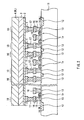
- FIG. 2 and FIG. 3 illustrate one example of the memory device (memory cell array) in which the plurality of memory elements 10 are disposed in matrix, wherein FIG. 2 and FIG. 3 illustrate a cross-sectional configuration and a planar configuration, respectively.
- each of the memory elements 10 is provided with a wire connected to the lower electrode 1 side thereof, and a wire connected to the upper electrode 4 side thereof, which are provided to intersect one another, and each of the memory elements 10 is disposed for example in the vicinity of the intersection of those wires.
- wiring connected on the upper electrode 4 side is formed in common on the entire array.
- each of the memory elements 10 shares the respective layers of the high-resistance layer 2, the ion source layer 3, and the upper electrode 4.
- each of the high-resistance layer 2, the ion source layer 3, and the upper electrode 4 is structured by a layer common to each of the memory elements 10 (identical layer).
- the commonly-formed upper electrode 4 is a plate electrode PL.
- the lower electrode 1 is formed individually for each memory cell. Thereby, each of the memory cells is electrically separated.
- the memory element 10 of each of the memory cells is defined by the lower electrode 1, provided for each of the memory cells, at a position corresponding to each lower electrode 1.
- Each of the lower electrodes 1 is connected to a corresponding cell-selection MOS transistor Tr, and each of the memory elements 10 is formed above the MOS transistor Tr.
- the MOS transistor Tr is structured with a source/drain region 13 formed in a region separated by an element separating layer 12 in the semiconductor substrate 11, and a gate electrode 14.
- a wall surface of the gate electrode 14 is formed with a side wall insulating layer.
- the gate electrode 14 also serves as a word line WL which is one of address wires of the memory element 10.
- One of the source/drain regions 13 of the MOS transistor Tr and the lower electrode 1 of the memory element 10 are electrically connected through a plug layer 15, a metal wiring layer 16, and a plug layer 17.
- the other of the source/drain regions 13 of the MOS transistor Tr is connected with the metal wiring layer 16 through the plug layer 15.
- the metal wiring layer 16 is connected with a bit line BL (see FIG. 3 ) as the other of the address wires of the memory element.
- BL bit line
- FIG. 3 note that an active region 18 of the MOS transistor Tr is indicated by a chained line.
- a contact portion 21 is connected with the lower electrode 1 of the memory element 10, and a contact portion 22 is connected with the bit line BL, respectively.
- the resistance value of the memory element 10 transits again to the high-resistance state. Thereby, the information recorded in the selected memory cell is erased.
- a memory cell is selected by the MOS transistor Tr and a predetermined voltage or current pulse is applied to that cell.
- a current or voltage, which is different in accordance with the resistance state of the memory element 10 at this time, is detected by the sense amplifier or the like connected to the bit line BL or to an end of the plate electrode PL. Meanwhile, the voltage or the current applied to the selected memory cell is configured to be smaller than a threshold value such as a voltage in which the state of the resistance value of the memory element 10 transits.
- the memory device can be applied to various memory devices as mentioned above. It is applicable to any memory mode, such as so-called PROM (Programmable Read Only Memory) in which writing is possible only once, EEPROM (Erasable Programmable Read Only Memory) in which the erasing is electrically possible, or so-called RAM in which the recording, the erasing, and the reproducing are possible at high speed, for example.
- PROM Program Memory
- EEPROM Erasable Programmable Read Only Memory
- RAM so-called RAM in which the recording, the erasing, and the reproducing are possible at high speed, for example.
- the MOS transistor was first formed on the semiconductor substrate 11. Then, an insulating layer was formed to cover a surface of the semiconductor substrate 11, and a via-hole was formed on the insulating layer. Subsequently, the inside of the via-hole was filled with an electrode material consisting of W (tungsten) with a CVD (Chemical Vapor Deposition) method, and a surface thereof was planarized with a CMP (Chemical Mechanical Polishing) method. In addition, these processes were repeated to form the plug layer 15, the metal wiring layer 16, the plug layer 17, and the lower electrode 1, and further, the lower electrode 1 was patterned for each memory cell. A size of an opening of the lower electrode 1 was configured with a diameter of 300 nm.
- etching was performed by about 1 nm with reverse sputtering utilizing a RF power source, in order to remove an oxide on an upper surface of the lower electrode 1.
- a surface of the lower electrode 1 was planarized such that the surface has a height virtually same as that of the surrounding insulating layer.
- the metal Gd film having a film-thickness of 1.0 nm was formed with DC magnetron sputtering, and further, the Gd film was oxidized for 10 seconds with RF plasma, with conditions of input power of 500 W and an atmosphere of O 2 under a chamber pressure of 1 mTorr. This Gd oxide was provided as the high-resistance layer 2.
- the ZrTeAl film was deposited as the ion source layer 3 on the high-resistance layer 2 to 45 nm.
- a composition thereof was Zr20% - Te40% -Al40% (atomic%).
- a W film was formed on the ion source layer 3 to a film-thickness of 20 nm as the upper electrode 4.
- a W film was formed as the upper electrode 4 on the ion source layer 3 to a film-thickness of 20 nm.
- Example 1 a surface of the upper electrode 4 was etched to expose a contact part to be connected with an external circuit for applying an intermediate potential (Vdd/2). Further, a wiring layer (Al layer) having a thickness of 200 nm was so formed as to be connected to the exposed contact part. Subsequently, a heat treatment was applied in a vacuum heat treatment furnace for 2 hours at a temperature of 300°C. In this manner, the memory cell array illustrated in FIG. 2 and FIG. 3 was fabricated to provide it as the Example 1. As below, memory cell arrays, each consisting of the memory element similar to that of the Example 1 except for the ion source layer 3, were fabricated to provide them as Examples 2 to 19 and Comparative Examples 1 to 4, respectively.
- Example 1 Zr was used as the metal element to be ionized for the ion source layer 3.
- Cu was used as the metal element to be ionized without using Al and Zr
- Si was used as the element which forms the oxide film in the erasing operation, to have a composition thereof: Cu - Te - Si.
- Comparative Example 2 Cu and Zr were used as the metal element to be ionized without using Al, and Si was used as the element which forms the oxide film in the erasing operation, to have a composition thereof: Cu - Zr - Te - Si.
- Example 1 By comparing the Example 1 with the Comparative Examples 1 and 2, effects in the cases in which Si and Al are used for the element considered to form the high-resistance layer (oxidization layer) by the erasing operation, and a difference in operating properties of memory between the case in which Zr is used for the metal element to be ionized and the case in which Cu is used therefor were studied.
- Comparative Examples 1 and 2 have the following compositions, and a film-thickness was 45 nm each.
- Comparative Example 1 Cu47% - Te25% - Si28% (atomic%)
- Comparative Example 2 Cu14% -Zr14% - Te27% - Si45% (atomic%)
- Example 2 Ta20% - Te40% - Al40% (atomic%)
- Example 3 Cr30% - Te30% - Al40% (atomic%)
- Example 4 Ti30% - Te30% - Al40% (atomic%)
- Example 5 W15% - Zr5% - Nb5% - Te35% - Al40% (atomic%)
- Films having the following composition ratios with the film-thicknesses of 45 nm were formed by using Zr as the metal element to be ionized of the ion source layer 3, respectively.
- Composition ratios of Al were varied from 10, 20, 30, 40, 50, and 60 to 70%, while ratios of Zr to Te were substantially constant.
- Example 3 Zr30% - Te60% - Al10% (atomic%)
- Example 6 Zr27% - Te53% -Al20% (atomic%)
- Example 7 Zr23% - Te47% - Al30% (atomic%)
- Example 8 Zr16% - Te34% - Al50% (atomic%)
- Example 9 Zr13% - Te27% - Al60% (atomic%)
- Comparative Example 4 Zr10% - Te20% - Al70% (atomic%)
- Films having the following composition ratios with the film-thicknesses of 45 nm were formed by using Zr and Cu as the metal element to be ionized of the ion source layer 3, respectively.
- Ratios of Zr and Cu were each represented by a fraction ratio of Zr / (Cu + Zr), and were varied from 1, 0.69, 0.5, 0.32, and 0.15 to 0.
- Example 10 Zr16% - Te44%-A140% (atomic%)
- Example 11 Zr11% - Cu5% - Te44% - Al40% (atomic%)
- Example 12 Zr8% - Cu8% - Te44% - Al40% (atomic%)
- Example 13 Zr10% - Cu21% - Te29% - Al44% (atomic%)
- Example 14 Zr5% - Cu28% - Te28% - Al39% (atomic%)
- Example 15 Cu45% - Te23% - Al32% (atomic%)
- Films having the following composition ratios with the film-thicknesses of 45 nm were formed by using Zr and Cu as the metal element to be ionized of the ion source layer 3, respectively.
- Ge and Si were added to Al as the element which forms the oxide in the erasing operation to provide them as the Examples 16 and 17, respectively.
- Mg Mg was used instead of Al was provided as the Example 18.
- Example 16 Zr8% - Cu8% - Te44% - Al35% - Ge5% (atomic%)
- the lower electrode 1 formed on the semiconductor substrate 11 having the CMOS circuit was covered with a SiO 2 film having a thickness of about 15 nm to provide an interlayer insulating film, in a similar manner as in the Example 1. Then, patterning utilizing electron lithography was performed to open a contact hole having a diameter of 20 nm on the interlayer insulating film. Thereafter, the ion source layer 3 having a composition of Zr8% - Cu8% - Te44% - Al40% (atomic%) was formed directly without forming the high-resistance layer 2, to fabricate a memory cell array similar to that of the Example 1, which was provided as the Example 19.
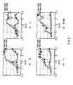
- the erasing voltages Ve were changed from 0.7 V to 2.5 V, in which a writing voltage Vw was 3.0 V, writing gate voltages Vgw were 1.3 V and 1.8 V, and an erasing gate voltage was 3.0 V, with pulse widths of 100 ns, 1 ⁇ s and 10 ⁇ s, respectively.
- a writing voltage Vw was 3.0 V
- writing gate voltages Vgw were 1.3 V and 1.8 V
- an erasing gate voltage was 3.0 V, with pulse widths of 100 ns, 1 ⁇ s and 10 ⁇ s, respectively.
- FIGs. 6(A) to (C) results of similar measurement performed by using a sample according to the Comparative Example 1, consisting of Cu - Te - Si based composition, with a similar method are as represented in FIGs. 6(A) to (C) .
- the pulse width by which a favorable retaining property is obtained and in which the writing and the erasure, i.e. the low-resistance state and the high-resistance state, are retained is until 10 ⁇ s, and they are hardly retained when the pulse width is shortened until 100 ns.
- FIGs. 7(A) to (C) represent results of similar measurement performed by utilizing a sample according to the Comparative Example 2 consisting of Cu - Zr - Te - Si based composition.
- the Example 1 uses Al
- the Comparative Examples 1 and 2 each uses Si, for the element which forms the high-resistance layer (oxidization layer) in the erasure, and by including Al
- the stability in the high speed operation enhances and the retaining properties in the writing and in the erasure resistance after the high speed operation are improved significantly in the Example 1.
- the Comparative Example 1 in which the operating ion, which takes a role in the memory operation is Cu
- the Example 1 in which it is Zr the recording retaining property in the case in which the writing is performed with the short pulse is greatly improved in the Example 1, since Zr is contained therein.
- the Comparative Example 2 which includes Zr but does not include Al
- the Example 1 which includes Zr and Al the erasing property is improved in the Example 1 which includes Al.
- FIG. 8 a result of measurement of the repetitive property of the sample according to the Comparative Example 2 with the same conditions as in FIG. 4 is as represented in FIG. 8 .
- the repetitive property in the Comparative Example 2 when compared with the Example 1, and deterioration is larger than the Example 1.
- operation at high speed is possible, and the data retaining property after the high speed operation becomes superior as well.
- the operating property was improved in the case where Zr was used as the carrier ion, as compared with the case where Cu was the carrier ion.
- the operating property having the superior retaining property after the high speed operation can be obtained as in Zr by including Al in the ion source layer 3.
- the cause thereof is not necessarily certain, it can be considered that this is because the conductive path in the metal state formed in the writing operation is stable in the solid electrolyte of chalcogenide such as Te when Zr, Ta, Cr, Ti or the like is used as the carrier ion, as compared with the case in which only Cu is used.
Landscapes
- Engineering & Computer Science (AREA)
- Computer Hardware Design (AREA)
- Semiconductor Memories (AREA)
Claims (9)
- Speicherelement (10) mit einer Speicherschicht (5), die eine Schicht mit Ionenquelle (3) zwischen einer ersten Elektrode und einer zweiten Elektrode umfasst und Informationen durch Änderung einer elektrischen Charakteristik der Speicherschicht (5) speichert, wobei
die Schicht mit Ionenquelle Al zusammen mit einem ionenleitenden Material und einem Metallelement, das ionisiert wird, enthält, dadurch gekennzeichnet, dass eine Menge von Al, das in der Schicht mit Ionenquelle (3) enthalten ist, zwischen 20 Atom% und 60 Atom%, beide inklusive, beträgt. - Speicherelement (10) nach Anspruch 1, wobei die Schicht mit Ionenquelle (3) mindestens eines von Ge, Mg und Si enthält.
- Speicherelement (10) nach Anspruch 1, wobei die Schicht mit Ionenquelle (3) mindestens eines der Übergangsmetallelemente Ti, Zr, Hf, V, Nb, Ta, Cr, Mo und W als Metallelement umfasst.
- Speicherelement (10) nach Anspruch 3, wobei das Metallelement mindestens eines von Zr, Ti und Cr ist.
- Speicherelement (10) nach Anspruch 3, wobei die Schicht mit Ionenquelle (3) Cu als Metallelement umfasst.
- Speicherelement (10) nach Anspruch 5, wobei ein Verhältnis zwischen dem Übergangsmetallelement und Cu in der Schicht mit Ionenquelle (3):

größer als 0,15 ist. - Speicherelement (10) nach Anspruch 1, wobei das ionenleitende Material der Speicherschicht (5) mindestens eines von S, Se und Te ist.
- Speicherelement (10) nach Anspruch 1, wobei die Speicherschicht (5) eine Schicht mit hohem Widerstand (2), der höher als ein Widerstandswert der Schicht mit Ionenquelle (3) ist, zwischen der Schicht mit Ionenquelle (3) und der ersten Elektrode aufweist.
- Speichervorrichtung, die eine Vielzahl von Speicherelementen (10) gemäß den Ansprüchen 1 bis 8 und eine Pulsanwendungsvorrichtung zur Anwendung eines Pulses einer Spannung oder eines Stroms selektiv zur Vielzahl der Speicherelemente (10) umfasst.
Applications Claiming Priority (2)
| Application Number | Priority Date | Filing Date | Title |
|---|---|---|---|
| JP2007204031A JP5088036B2 (ja) | 2007-08-06 | 2007-08-06 | 記憶素子および記憶装置 |
| PCT/JP2008/063761 WO2009020041A1 (ja) | 2007-08-06 | 2008-07-31 | 記憶素子および記憶装置 |
Publications (3)
| Publication Number | Publication Date |
|---|---|
| EP2178122A1 EP2178122A1 (de) | 2010-04-21 |
| EP2178122A4 EP2178122A4 (de) | 2011-08-31 |
| EP2178122B1 true EP2178122B1 (de) | 2012-11-28 |
Family
ID=40341275
Family Applications (1)
| Application Number | Title | Priority Date | Filing Date |
|---|---|---|---|
| EP08791976A Not-in-force EP2178122B1 (de) | 2007-08-06 | 2008-07-31 | Speicherelement und speichervorrichtung |
Country Status (7)
| Country | Link |
|---|---|
| US (1) | US8492740B2 (de) |
| EP (1) | EP2178122B1 (de) |
| JP (1) | JP5088036B2 (de) |
| KR (1) | KR101496281B1 (de) |
| CN (1) | CN101765914B (de) |
| TW (1) | TWI489622B (de) |
| WO (1) | WO2009020041A1 (de) |
Families Citing this family (47)
| Publication number | Priority date | Publication date | Assignee | Title |
|---|---|---|---|---|
| US7768812B2 (en) | 2008-01-15 | 2010-08-03 | Micron Technology, Inc. | Memory cells, memory cell programming methods, memory cell reading methods, memory cell operating methods, and memory devices |
| US8034655B2 (en) | 2008-04-08 | 2011-10-11 | Micron Technology, Inc. | Non-volatile resistive oxide memory cells, non-volatile resistive oxide memory arrays, and methods of forming non-volatile resistive oxide memory cells and memory arrays |
| US8211743B2 (en) | 2008-05-02 | 2012-07-03 | Micron Technology, Inc. | Methods of forming non-volatile memory cells having multi-resistive state material between conductive electrodes |
| US8134137B2 (en) | 2008-06-18 | 2012-03-13 | Micron Technology, Inc. | Memory device constructions, memory cell forming methods, and semiconductor construction forming methods |
| US9343665B2 (en) | 2008-07-02 | 2016-05-17 | Micron Technology, Inc. | Methods of forming a non-volatile resistive oxide memory cell and methods of forming a non-volatile resistive oxide memory array |
| TW201011909A (en) * | 2008-09-02 | 2010-03-16 | Sony Corp | Storage element and storage device |
| WO2010150720A1 (ja) * | 2009-06-25 | 2010-12-29 | 日本電気株式会社 | 半導体装置及びその製造方法 |
| US9059402B2 (en) | 2009-06-25 | 2015-06-16 | Nec Corporation | Resistance-variable element and method for manufacturing the same |
| JP5377142B2 (ja) | 2009-07-28 | 2013-12-25 | ソニー株式会社 | ターゲットの製造方法、メモリの製造方法 |
| JP2011124511A (ja) | 2009-12-14 | 2011-06-23 | Sony Corp | 記憶素子および記憶装置 |
| JP5630021B2 (ja) * | 2010-01-19 | 2014-11-26 | ソニー株式会社 | 記憶素子および記憶装置 |
| US8427859B2 (en) | 2010-04-22 | 2013-04-23 | Micron Technology, Inc. | Arrays of vertically stacked tiers of non-volatile cross point memory cells, methods of forming arrays of vertically stacked tiers of non-volatile cross point memory cells, and methods of reading a data value stored by an array of vertically stacked tiers of non-volatile cross point memory cells |
| US8411477B2 (en) | 2010-04-22 | 2013-04-02 | Micron Technology, Inc. | Arrays of vertically stacked tiers of non-volatile cross point memory cells, methods of forming arrays of vertically stacked tiers of non-volatile cross point memory cells, and methods of reading a data value stored by an array of vertically stacked tiers of non-volatile cross point memory cells |
| US8289763B2 (en) | 2010-06-07 | 2012-10-16 | Micron Technology, Inc. | Memory arrays |
| JP2012019042A (ja) | 2010-07-07 | 2012-01-26 | Sony Corp | 記憶素子および記憶装置 |
| JP2012064808A (ja) | 2010-09-16 | 2012-03-29 | Sony Corp | 記憶素子および記憶装置 |
| US8351242B2 (en) | 2010-09-29 | 2013-01-08 | Micron Technology, Inc. | Electronic devices, memory devices and memory arrays |
| US8759809B2 (en) | 2010-10-21 | 2014-06-24 | Micron Technology, Inc. | Integrated circuitry comprising nonvolatile memory cells having platelike electrode and ion conductive material layer |
| US8526213B2 (en) | 2010-11-01 | 2013-09-03 | Micron Technology, Inc. | Memory cells, methods of programming memory cells, and methods of forming memory cells |
| US8796661B2 (en) | 2010-11-01 | 2014-08-05 | Micron Technology, Inc. | Nonvolatile memory cells and methods of forming nonvolatile memory cell |
| US9454997B2 (en) | 2010-12-02 | 2016-09-27 | Micron Technology, Inc. | Array of nonvolatile memory cells having at least five memory cells per unit cell, having a plurality of the unit cells which individually comprise three elevational regions of programmable material, and/or having a continuous volume having a combination of a plurality of vertically oriented memory cells and a plurality of horizontally oriented memory cells; array of vertically stacked tiers of nonvolatile memory cells |
| JP5728919B2 (ja) * | 2010-12-09 | 2015-06-03 | ソニー株式会社 | 記憶素子および記憶装置 |
| JP2012128892A (ja) | 2010-12-13 | 2012-07-05 | Sony Corp | 記憶装置 |
| US8431458B2 (en) | 2010-12-27 | 2013-04-30 | Micron Technology, Inc. | Methods of forming a nonvolatile memory cell and methods of forming an array of nonvolatile memory cells |
| US8791447B2 (en) | 2011-01-20 | 2014-07-29 | Micron Technology, Inc. | Arrays of nonvolatile memory cells and methods of forming arrays of nonvolatile memory cells |
| US8488365B2 (en) | 2011-02-24 | 2013-07-16 | Micron Technology, Inc. | Memory cells |
| JP2012182172A (ja) | 2011-02-28 | 2012-09-20 | Sony Corp | 記憶素子および記憶装置 |
| JP2012186316A (ja) | 2011-03-04 | 2012-09-27 | Sony Corp | 記憶素子および記憶装置 |
| US8537592B2 (en) | 2011-04-15 | 2013-09-17 | Micron Technology, Inc. | Arrays of nonvolatile memory cells and methods of forming arrays of nonvolatile memory cells |
| US8531867B2 (en) * | 2011-05-05 | 2013-09-10 | Adesto Technologies Corporation | Conductive filament based memory elements and methods with improved data retention and/or endurance |
| US9230797B2 (en) | 2011-05-26 | 2016-01-05 | Empire Technology Development Llc | Dielectric and/or capacitor formation |
| CN102222763A (zh) * | 2011-06-03 | 2011-10-19 | 复旦大学 | 一种采用电场增强层的阻变存储器结构及其制备方法 |
| JP5724651B2 (ja) * | 2011-06-10 | 2015-05-27 | ソニー株式会社 | 記憶素子および記憶装置 |
| JP2013016530A (ja) | 2011-06-30 | 2013-01-24 | Sony Corp | 記憶素子およびその製造方法ならびに記憶装置 |
| JP5708930B2 (ja) * | 2011-06-30 | 2015-04-30 | ソニー株式会社 | 記憶素子およびその製造方法ならびに記憶装置 |
| US9318699B2 (en) | 2012-01-18 | 2016-04-19 | Micron Technology, Inc. | Resistive memory cell structures and methods |
| US9099633B2 (en) | 2012-03-26 | 2015-08-04 | Adesto Technologies Corporation | Solid electrolyte memory elements with electrode interface for improved performance |
| US8598560B1 (en) * | 2012-07-12 | 2013-12-03 | Micron Technology, Inc. | Resistive memory elements exhibiting increased interfacial adhesion strength, methods of forming the same, and related resistive memory cells and memory devices |
| KR20140035558A (ko) | 2012-09-14 | 2014-03-24 | 삼성전자주식회사 | 가변 저항 메모리 장치 및 그 동작 방법 |
| CN103074583B (zh) * | 2013-01-25 | 2015-04-22 | 合肥工业大学 | 一种cigs薄膜电池的激光沉积制备工艺 |
| US20180033960A1 (en) * | 2013-03-15 | 2018-02-01 | Adesto Technologies Corporation | Nonvolatile memory elements having conductive structures with semimetals and/or semiconductors |
| US9184377B2 (en) | 2013-06-11 | 2015-11-10 | Micron Technology, Inc. | Resistance variable memory cell structures and methods |
| WO2016186148A1 (ja) * | 2015-05-18 | 2016-11-24 | 国立大学法人東北大学 | 記憶セル、記憶回路、及び記憶方法 |
| TWI559305B (zh) * | 2015-08-07 | 2016-11-21 | Univ Chang Gung | Resistive memory with multiple resistive states |
| US9431606B1 (en) * | 2015-08-12 | 2016-08-30 | Micron Technology, Inc. | Memory cells |
| FR3066323B1 (fr) * | 2017-05-12 | 2019-11-01 | Commissariat A L'energie Atomique Et Aux Energies Alternatives | Memoire non volatile favorisant une grande densite d'integration |
| WO2022095007A1 (en) * | 2020-11-09 | 2022-05-12 | Yangtze Advanced Memory Industrial Innovation Center Co., Ltd | Memory devices having memory cells with multiple threshold voltages and methods for forming and operating the same |
Family Cites Families (14)
| Publication number | Priority date | Publication date | Assignee | Title |
|---|---|---|---|---|
| US6635914B2 (en) * | 2000-09-08 | 2003-10-21 | Axon Technologies Corp. | Microelectronic programmable device and methods of forming and programming the same |
| JP2002536840A (ja) | 1999-02-11 | 2002-10-29 | アリゾナ ボード オブ リージェンツ | プログラマブルマイクロエレクトロニックデバイスおよびその形成およびプログラミング方法 |
| JP2003060083A (ja) * | 2001-08-10 | 2003-02-28 | Matsushita Electric Ind Co Ltd | 半導体記憶装置およびその駆動方法 |
| JP2003060090A (ja) * | 2001-08-10 | 2003-02-28 | Matsushita Electric Ind Co Ltd | 不揮発性半導体記憶装置、その駆動方法及び製造方法 |
| US6709958B2 (en) * | 2001-08-30 | 2004-03-23 | Micron Technology, Inc. | Integrated circuit device and fabrication using metal-doped chalcogenide materials |
| US7116573B2 (en) * | 2003-07-18 | 2006-10-03 | Nec Corporation | Switching element method of driving switching element rewritable logic integrated circuit and memory |
| JP4766441B2 (ja) * | 2003-09-17 | 2011-09-07 | 三菱マテリアル株式会社 | 半導体不揮発メモリー用相変化膜およびこの相変化膜を形成するためのスパッタリングターゲット |
| DE102005003675A1 (de) * | 2004-04-29 | 2005-11-24 | Infineon Technologies Ag | CBRAM-Zelle mit einem reversiblen Leitungsbrücken-Mechanismus |
| DE102004052647B4 (de) * | 2004-10-29 | 2009-01-02 | Qimonda Ag | Methode zur Verbesserung der thermischen Eigenschaften von Halbleiter-Speicherzellen im Herstellungsverfahren und nichtflüchtige, resistiv schaltende Speicherzelle |
| DE102005005938B4 (de) | 2005-02-09 | 2009-04-30 | Qimonda Ag | Resistives Speicherelement mit verkürzter Löschzeit, Verfahren zur Herstellung und Speicherzellen-Anordnung |
| JP2007026492A (ja) * | 2005-07-13 | 2007-02-01 | Sony Corp | 記憶装置及び半導体装置 |
| WO2007069725A1 (ja) * | 2005-12-15 | 2007-06-21 | Nec Corporation | スイッチング素子およびその製造方法 |
| JP4760516B2 (ja) | 2005-12-15 | 2011-08-31 | 東京エレクトロン株式会社 | 塗布装置及び塗布方法 |
| EP1835509A1 (de) * | 2006-03-14 | 2007-09-19 | Qimonda AG | Speicherzelle, Speicher mit einer Speicherzelle und Verfahren zum Einschreiben von Daten in eine Speicherzelle |
-
2007
- 2007-08-06 JP JP2007204031A patent/JP5088036B2/ja not_active Expired - Fee Related
-
2008
- 2008-07-31 US US12/670,887 patent/US8492740B2/en active Active - Reinstated
- 2008-07-31 EP EP08791976A patent/EP2178122B1/de not_active Not-in-force
- 2008-07-31 KR KR1020107000797A patent/KR101496281B1/ko not_active Expired - Fee Related
- 2008-07-31 WO PCT/JP2008/063761 patent/WO2009020041A1/ja not_active Ceased
- 2008-07-31 CN CN2008801012564A patent/CN101765914B/zh not_active Expired - Fee Related
- 2008-08-04 TW TW097129532A patent/TWI489622B/zh not_active IP Right Cessation
Also Published As
| Publication number | Publication date |
|---|---|
| EP2178122A4 (de) | 2011-08-31 |
| WO2009020041A1 (ja) | 2009-02-12 |
| TWI489622B (zh) | 2015-06-21 |
| KR20100050452A (ko) | 2010-05-13 |
| TW200915561A (en) | 2009-04-01 |
| CN101765914B (zh) | 2012-09-26 |
| JP2009043757A (ja) | 2009-02-26 |
| US8492740B2 (en) | 2013-07-23 |
| EP2178122A1 (de) | 2010-04-21 |
| CN101765914A (zh) | 2010-06-30 |
| KR101496281B1 (ko) | 2015-02-26 |
| US20100195371A1 (en) | 2010-08-05 |
| JP5088036B2 (ja) | 2012-12-05 |
Similar Documents
| Publication | Publication Date | Title |
|---|---|---|
| EP2178122B1 (de) | Speicherelement und speichervorrichtung | |
| TWI443821B (zh) | A memory element and a memory device, and a method of operating the memory device | |
| US8350248B2 (en) | Memory element and memory device | |
| TWI472018B (zh) | Memory elements and memory devices | |
| US7307270B2 (en) | Memory element and memory device | |
| JP4539885B2 (ja) | 記憶素子および記憶装置 | |
| KR101519696B1 (ko) | 기억 소자 및 기억 장치 | |
| US7786459B2 (en) | Memory element and memory device comprising memory layer positioned between first and second electrodes | |
| JP2009043873A (ja) | 記憶素子および記憶装置 | |
| JP5708930B2 (ja) | 記憶素子およびその製造方法ならびに記憶装置 | |
| TWI497491B (zh) | 記憶體元件及記憶體裝置 | |
| JP2012018964A (ja) | 記憶素子およびその駆動方法、並びに記憶装置 | |
| JP4396621B2 (ja) | 記憶素子及び記憶装置 | |
| JP5724651B2 (ja) | 記憶素子および記憶装置 | |
| JP4465969B2 (ja) | 半導体記憶素子及びこれを用いた半導体記憶装置 | |
| JP5257573B2 (ja) | 記憶素子および記憶装置 |
Legal Events
| Date | Code | Title | Description |
|---|---|---|---|
| PUAI | Public reference made under article 153(3) epc to a published international application that has entered the european phase |
Free format text: ORIGINAL CODE: 0009012 |
|
| 17P | Request for examination filed |
Effective date: 20100122 |
|
| AK | Designated contracting states |
Kind code of ref document: A1 Designated state(s): AT BE BG CH CY CZ DE DK EE ES FI FR GB GR HR HU IE IS IT LI LT LU LV MC MT NL NO PL PT RO SE SI SK TR |
|
| AX | Request for extension of the european patent |
Extension state: AL BA MK RS |
|
| DAX | Request for extension of the european patent (deleted) | ||
| A4 | Supplementary search report drawn up and despatched |
Effective date: 20110729 |
|
| RIC1 | Information provided on ipc code assigned before grant |
Ipc: H01L 49/00 20060101ALI20110725BHEP Ipc: G11C 13/02 20060101ALI20110725BHEP Ipc: H01L 45/00 20060101ALI20110725BHEP Ipc: H01L 27/10 20060101AFI20110725BHEP |
|
| 17Q | First examination report despatched |
Effective date: 20110817 |
|
| GRAP | Despatch of communication of intention to grant a patent |
Free format text: ORIGINAL CODE: EPIDOSNIGR1 |
|
| RIC1 | Information provided on ipc code assigned before grant |
Ipc: G11C 13/02 20060101ALI20120514BHEP Ipc: H01L 45/00 20060101ALI20120514BHEP Ipc: H01L 27/10 20060101AFI20120514BHEP |
|
| GRAS | Grant fee paid |
Free format text: ORIGINAL CODE: EPIDOSNIGR3 |
|
| GRAA | (expected) grant |
Free format text: ORIGINAL CODE: 0009210 |
|
| AK | Designated contracting states |
Kind code of ref document: B1 Designated state(s): AT BE BG CH CY CZ DE DK EE ES FI FR GB GR HR HU IE IS IT LI LT LU LV MC MT NL NO PL PT RO SE SI SK TR |
|
| REG | Reference to a national code |
Ref country code: GB Ref legal event code: FG4D |
|
| REG | Reference to a national code |
Ref country code: CH Ref legal event code: EP |
|
| REG | Reference to a national code |
Ref country code: AT Ref legal event code: REF Ref document number: 586564 Country of ref document: AT Kind code of ref document: T Effective date: 20121215 |
|
| REG | Reference to a national code |
Ref country code: IE Ref legal event code: FG4D |
|
| REG | Reference to a national code |
Ref country code: DE Ref legal event code: R096 Ref document number: 602008020472 Country of ref document: DE Effective date: 20130124 |
|
| REG | Reference to a national code |
Ref country code: AT Ref legal event code: MK05 Ref document number: 586564 Country of ref document: AT Kind code of ref document: T Effective date: 20121128 |
|
| REG | Reference to a national code |
Ref country code: NL Ref legal event code: VDEP Effective date: 20121128 |
|
| REG | Reference to a national code |
Ref country code: LT Ref legal event code: MG4D |
|
| PG25 | Lapsed in a contracting state [announced via postgrant information from national office to epo] |
Ref country code: HR Free format text: LAPSE BECAUSE OF FAILURE TO SUBMIT A TRANSLATION OF THE DESCRIPTION OR TO PAY THE FEE WITHIN THE PRESCRIBED TIME-LIMIT Effective date: 20121128 Ref country code: ES Free format text: LAPSE BECAUSE OF FAILURE TO SUBMIT A TRANSLATION OF THE DESCRIPTION OR TO PAY THE FEE WITHIN THE PRESCRIBED TIME-LIMIT Effective date: 20130311 Ref country code: SE Free format text: LAPSE BECAUSE OF FAILURE TO SUBMIT A TRANSLATION OF THE DESCRIPTION OR TO PAY THE FEE WITHIN THE PRESCRIBED TIME-LIMIT Effective date: 20121128 Ref country code: NO Free format text: LAPSE BECAUSE OF FAILURE TO SUBMIT A TRANSLATION OF THE DESCRIPTION OR TO PAY THE FEE WITHIN THE PRESCRIBED TIME-LIMIT Effective date: 20130228 Ref country code: LT Free format text: LAPSE BECAUSE OF FAILURE TO SUBMIT A TRANSLATION OF THE DESCRIPTION OR TO PAY THE FEE WITHIN THE PRESCRIBED TIME-LIMIT Effective date: 20121128 Ref country code: FI Free format text: LAPSE BECAUSE OF FAILURE TO SUBMIT A TRANSLATION OF THE DESCRIPTION OR TO PAY THE FEE WITHIN THE PRESCRIBED TIME-LIMIT Effective date: 20121128 |
|
| PG25 | Lapsed in a contracting state [announced via postgrant information from national office to epo] |
Ref country code: PL Free format text: LAPSE BECAUSE OF FAILURE TO SUBMIT A TRANSLATION OF THE DESCRIPTION OR TO PAY THE FEE WITHIN THE PRESCRIBED TIME-LIMIT Effective date: 20121128 Ref country code: BE Free format text: LAPSE BECAUSE OF FAILURE TO SUBMIT A TRANSLATION OF THE DESCRIPTION OR TO PAY THE FEE WITHIN THE PRESCRIBED TIME-LIMIT Effective date: 20121128 Ref country code: PT Free format text: LAPSE BECAUSE OF FAILURE TO SUBMIT A TRANSLATION OF THE DESCRIPTION OR TO PAY THE FEE WITHIN THE PRESCRIBED TIME-LIMIT Effective date: 20130328 Ref country code: LV Free format text: LAPSE BECAUSE OF FAILURE TO SUBMIT A TRANSLATION OF THE DESCRIPTION OR TO PAY THE FEE WITHIN THE PRESCRIBED TIME-LIMIT Effective date: 20121128 Ref country code: GR Free format text: LAPSE BECAUSE OF FAILURE TO SUBMIT A TRANSLATION OF THE DESCRIPTION OR TO PAY THE FEE WITHIN THE PRESCRIBED TIME-LIMIT Effective date: 20130301 Ref country code: SI Free format text: LAPSE BECAUSE OF FAILURE TO SUBMIT A TRANSLATION OF THE DESCRIPTION OR TO PAY THE FEE WITHIN THE PRESCRIBED TIME-LIMIT Effective date: 20121128 |
|
| PG25 | Lapsed in a contracting state [announced via postgrant information from national office to epo] |
Ref country code: AT Free format text: LAPSE BECAUSE OF FAILURE TO SUBMIT A TRANSLATION OF THE DESCRIPTION OR TO PAY THE FEE WITHIN THE PRESCRIBED TIME-LIMIT Effective date: 20121128 |
|
| PG25 | Lapsed in a contracting state [announced via postgrant information from national office to epo] |
Ref country code: EE Free format text: LAPSE BECAUSE OF FAILURE TO SUBMIT A TRANSLATION OF THE DESCRIPTION OR TO PAY THE FEE WITHIN THE PRESCRIBED TIME-LIMIT Effective date: 20121128 Ref country code: SK Free format text: LAPSE BECAUSE OF FAILURE TO SUBMIT A TRANSLATION OF THE DESCRIPTION OR TO PAY THE FEE WITHIN THE PRESCRIBED TIME-LIMIT Effective date: 20121128 Ref country code: DK Free format text: LAPSE BECAUSE OF FAILURE TO SUBMIT A TRANSLATION OF THE DESCRIPTION OR TO PAY THE FEE WITHIN THE PRESCRIBED TIME-LIMIT Effective date: 20121128 Ref country code: BG Free format text: LAPSE BECAUSE OF FAILURE TO SUBMIT A TRANSLATION OF THE DESCRIPTION OR TO PAY THE FEE WITHIN THE PRESCRIBED TIME-LIMIT Effective date: 20130228 Ref country code: CZ Free format text: LAPSE BECAUSE OF FAILURE TO SUBMIT A TRANSLATION OF THE DESCRIPTION OR TO PAY THE FEE WITHIN THE PRESCRIBED TIME-LIMIT Effective date: 20121128 |
|
| PG25 | Lapsed in a contracting state [announced via postgrant information from national office to epo] |
Ref country code: IT Free format text: LAPSE BECAUSE OF FAILURE TO SUBMIT A TRANSLATION OF THE DESCRIPTION OR TO PAY THE FEE WITHIN THE PRESCRIBED TIME-LIMIT Effective date: 20121128 Ref country code: NL Free format text: LAPSE BECAUSE OF FAILURE TO SUBMIT A TRANSLATION OF THE DESCRIPTION OR TO PAY THE FEE WITHIN THE PRESCRIBED TIME-LIMIT Effective date: 20121128 Ref country code: RO Free format text: LAPSE BECAUSE OF FAILURE TO SUBMIT A TRANSLATION OF THE DESCRIPTION OR TO PAY THE FEE WITHIN THE PRESCRIBED TIME-LIMIT Effective date: 20121128 |
|
| PLBE | No opposition filed within time limit |
Free format text: ORIGINAL CODE: 0009261 |
|
| STAA | Information on the status of an ep patent application or granted ep patent |
Free format text: STATUS: NO OPPOSITION FILED WITHIN TIME LIMIT |
|
| 26N | No opposition filed |
Effective date: 20130829 |
|
| PG25 | Lapsed in a contracting state [announced via postgrant information from national office to epo] |
Ref country code: CY Free format text: LAPSE BECAUSE OF FAILURE TO SUBMIT A TRANSLATION OF THE DESCRIPTION OR TO PAY THE FEE WITHIN THE PRESCRIBED TIME-LIMIT Effective date: 20121128 |
|
| REG | Reference to a national code |
Ref country code: DE Ref legal event code: R097 Ref document number: 602008020472 Country of ref document: DE Effective date: 20130829 |
|
| PG25 | Lapsed in a contracting state [announced via postgrant information from national office to epo] |
Ref country code: MC Free format text: LAPSE BECAUSE OF FAILURE TO SUBMIT A TRANSLATION OF THE DESCRIPTION OR TO PAY THE FEE WITHIN THE PRESCRIBED TIME-LIMIT Effective date: 20121128 |
|
| REG | Reference to a national code |
Ref country code: CH Ref legal event code: PL |
|
| REG | Reference to a national code |
Ref country code: IE Ref legal event code: MM4A |
|
| PG25 | Lapsed in a contracting state [announced via postgrant information from national office to epo] |
Ref country code: LI Free format text: LAPSE BECAUSE OF NON-PAYMENT OF DUE FEES Effective date: 20130731 Ref country code: CH Free format text: LAPSE BECAUSE OF NON-PAYMENT OF DUE FEES Effective date: 20130731 |
|
| PG25 | Lapsed in a contracting state [announced via postgrant information from national office to epo] |
Ref country code: IE Free format text: LAPSE BECAUSE OF NON-PAYMENT OF DUE FEES Effective date: 20130731 |
|
| PGFP | Annual fee paid to national office [announced via postgrant information from national office to epo] |
Ref country code: DE Payment date: 20140721 Year of fee payment: 7 |
|
| PGFP | Annual fee paid to national office [announced via postgrant information from national office to epo] |
Ref country code: FR Payment date: 20140721 Year of fee payment: 7 Ref country code: GB Payment date: 20140721 Year of fee payment: 7 |
|
| PG25 | Lapsed in a contracting state [announced via postgrant information from national office to epo] |
Ref country code: MT Free format text: LAPSE BECAUSE OF FAILURE TO SUBMIT A TRANSLATION OF THE DESCRIPTION OR TO PAY THE FEE WITHIN THE PRESCRIBED TIME-LIMIT Effective date: 20121128 Ref country code: TR Free format text: LAPSE BECAUSE OF FAILURE TO SUBMIT A TRANSLATION OF THE DESCRIPTION OR TO PAY THE FEE WITHIN THE PRESCRIBED TIME-LIMIT Effective date: 20121128 |
|
| PG25 | Lapsed in a contracting state [announced via postgrant information from national office to epo] |
Ref country code: HU Free format text: LAPSE BECAUSE OF FAILURE TO SUBMIT A TRANSLATION OF THE DESCRIPTION OR TO PAY THE FEE WITHIN THE PRESCRIBED TIME-LIMIT; INVALID AB INITIO Effective date: 20080731 Ref country code: LU Free format text: LAPSE BECAUSE OF NON-PAYMENT OF DUE FEES Effective date: 20130731 |
|
| REG | Reference to a national code |
Ref country code: DE Ref legal event code: R119 Ref document number: 602008020472 Country of ref document: DE |
|
| GBPC | Gb: european patent ceased through non-payment of renewal fee |
Effective date: 20150731 |
|
| PG25 | Lapsed in a contracting state [announced via postgrant information from national office to epo] |
Ref country code: DE Free format text: LAPSE BECAUSE OF NON-PAYMENT OF DUE FEES Effective date: 20160202 Ref country code: GB Free format text: LAPSE BECAUSE OF NON-PAYMENT OF DUE FEES Effective date: 20150731 |
|
| REG | Reference to a national code |
Ref country code: FR Ref legal event code: ST Effective date: 20160331 |
|
| PG25 | Lapsed in a contracting state [announced via postgrant information from national office to epo] |
Ref country code: FR Free format text: LAPSE BECAUSE OF NON-PAYMENT OF DUE FEES Effective date: 20150731 |
|
| PG25 | Lapsed in a contracting state [announced via postgrant information from national office to epo] |
Ref country code: IS Free format text: LAPSE BECAUSE OF FAILURE TO SUBMIT A TRANSLATION OF THE DESCRIPTION OR TO PAY THE FEE WITHIN THE PRESCRIBED TIME-LIMIT Effective date: 20121128 |