EP2174762B1 - Method for scribing bonded substrates - Google Patents
Method for scribing bonded substrates Download PDFInfo
- Publication number
- EP2174762B1 EP2174762B1 EP09171792.6A EP09171792A EP2174762B1 EP 2174762 B1 EP2174762 B1 EP 2174762B1 EP 09171792 A EP09171792 A EP 09171792A EP 2174762 B1 EP2174762 B1 EP 2174762B1
- Authority
- EP
- European Patent Office
- Prior art keywords
- substrate
- scribe lines
- products
- created
- scribe
- Prior art date
- Legal status (The legal status is an assumption and is not a legal conclusion. Google has not performed a legal analysis and makes no representation as to the accuracy of the status listed.)
- Not-in-force
Links
- 239000000758 substrate Substances 0.000 title claims description 167
- 238000000034 method Methods 0.000 title claims description 39
- 239000000463 material Substances 0.000 claims description 24
- 239000003566 sealing material Substances 0.000 claims description 14
- 238000010586 diagram Methods 0.000 description 8
- 230000008602 contraction Effects 0.000 description 7
- 239000004973 liquid crystal related substance Substances 0.000 description 6
- 239000011521 glass Substances 0.000 description 4
- 238000005452 bending Methods 0.000 description 2
- 230000000694 effects Effects 0.000 description 2
- 239000000919 ceramic Substances 0.000 description 1
- 238000004891 communication Methods 0.000 description 1
- 230000007547 defect Effects 0.000 description 1
- 238000005516 engineering process Methods 0.000 description 1
- 229910021421 monocrystalline silicon Inorganic materials 0.000 description 1
- 229910052594 sapphire Inorganic materials 0.000 description 1
- 239000010980 sapphire Substances 0.000 description 1
- 239000004065 semiconductor Substances 0.000 description 1
- 239000010409 thin film Substances 0.000 description 1
- 235000012431 wafers Nutrition 0.000 description 1
Images
Classifications
-
- B—PERFORMING OPERATIONS; TRANSPORTING
- B28—WORKING CEMENT, CLAY, OR STONE
- B28D—WORKING STONE OR STONE-LIKE MATERIALS
- B28D1/00—Working stone or stone-like materials, e.g. brick, concrete or glass, not provided for elsewhere; Machines, devices, tools therefor
- B28D1/22—Working stone or stone-like materials, e.g. brick, concrete or glass, not provided for elsewhere; Machines, devices, tools therefor by cutting, e.g. incising
- B28D1/225—Working stone or stone-like materials, e.g. brick, concrete or glass, not provided for elsewhere; Machines, devices, tools therefor by cutting, e.g. incising for scoring or breaking, e.g. tiles
-
- C—CHEMISTRY; METALLURGY
- C03—GLASS; MINERAL OR SLAG WOOL
- C03B—MANUFACTURE, SHAPING, OR SUPPLEMENTARY PROCESSES
- C03B33/00—Severing cooled glass
- C03B33/07—Cutting armoured, multi-layered, coated or laminated, glass products
-
- B—PERFORMING OPERATIONS; TRANSPORTING
- B28—WORKING CEMENT, CLAY, OR STONE
- B28D—WORKING STONE OR STONE-LIKE MATERIALS
- B28D5/00—Fine working of gems, jewels, crystals, e.g. of semiconductor material; apparatus or devices therefor
- B28D5/0005—Fine working of gems, jewels, crystals, e.g. of semiconductor material; apparatus or devices therefor by breaking, e.g. dicing
- B28D5/0011—Fine working of gems, jewels, crystals, e.g. of semiconductor material; apparatus or devices therefor by breaking, e.g. dicing with preliminary treatment, e.g. weakening by scoring
-
- G—PHYSICS
- G02—OPTICS
- G02F—OPTICAL DEVICES OR ARRANGEMENTS FOR THE CONTROL OF LIGHT BY MODIFICATION OF THE OPTICAL PROPERTIES OF THE MEDIA OF THE ELEMENTS INVOLVED THEREIN; NON-LINEAR OPTICS; FREQUENCY-CHANGING OF LIGHT; OPTICAL LOGIC ELEMENTS; OPTICAL ANALOGUE/DIGITAL CONVERTERS
- G02F1/00—Devices or arrangements for the control of the intensity, colour, phase, polarisation or direction of light arriving from an independent light source, e.g. switching, gating or modulating; Non-linear optics
- G02F1/01—Devices or arrangements for the control of the intensity, colour, phase, polarisation or direction of light arriving from an independent light source, e.g. switching, gating or modulating; Non-linear optics for the control of the intensity, phase, polarisation or colour
- G02F1/13—Devices or arrangements for the control of the intensity, colour, phase, polarisation or direction of light arriving from an independent light source, e.g. switching, gating or modulating; Non-linear optics for the control of the intensity, phase, polarisation or colour based on liquid crystals, e.g. single liquid crystal display cells
Definitions
- the present invention relates to a method for scribing bonded substrates made of a brittle material using a scribing wheel.
- the brittle material includes glass substrates, such as FPD's, and those for portable communication apparatuses, ceramics, single crystal silicon, semiconductor wafers and sapphire.
- US20040123717A1 shows a method for scribing bonded substrates, where a substrate to be processed has a substrate structure where a first substrate and a second substrate are bonded together with a sealing material so that a number of products are formed in locations respectively including a sealing material in said substrate structure and an end material region is formed between adjacent products, according to which scribe lines are created in a first and second substrate along which products are cut out using a scribing wheel, comprising the steps of:
- liquid crystal display panels have a structure where a color filter is formed on one substrate and TFT's (thin film transistors) for driving the liquid crystal are formed on the other substrate, and the two substrates are bonded together with liquid crystal in between.
- TFT's thin film transistors
- Such liquid crystal display panels are manufactured by forming a number of unit display panels, each of which is to become a liquid crystal display panel, in a bonded substrate (mother substrate) having a large area, and cutting out the respective unit display panels (see Patent Document 1).
- Patent Document 1 Japanese Unexamined Patent Publication H06 (1994)-48755 also represents prior art.
- a first substrate and a second substrate are bonded together with a sealing material.
- lines along which products are cut out from the bonded substrate are set on the bonded substrate and scribe lines are created in the two respective substrates along these lines along which products are cut out, and then a breaking process for applying stress along these scribe lines is carried out, and thus, products are cut out.
- These scribe lines include scribe lines for outlines created along the outline of products and auxiliary scribe lines created in an end material region between adjacent products in order to assist cutting.
- scribe lines created in a bonded substrate are described.
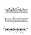
- Figs 3(a) and 3(b) are schematic cross sectional diagrams showing a bonded substrate.
- a first substrate G1 and a second substrate G2 are secured to each other by means of a sealing material S1 and a sealing material S2.
- the scribe line SL1 created in the vicinity of the sealing material S1 provides a border Ca for a first product R1 on the left side of the border Ca
- the scribe line SL3 created in the vicinity of the sealing material S2 provides a border Cb for a second product R2 on the right side of the border Cb, and thus, the region sandwiched between the borders (between Ca and Cb) becomes an end material region Q.
- a terminal process for forming a terminal is carried out in some end material regions when each product is cut out.
- products can be cut out in the same manner along scribe lines in the case where terminals are formed.
- scribing process A process for creating a scribe line (hereinafter referred to as scribing process) in a concrete example according to the prior art is described below.
- scribe lines SL1 and SL3 are created along the borders Ca and Cb on one substrate (here, the first substrate G1) using a scribing wheel W1 in accordance with a scribing process.
- scribe lines SL2 and SL4 are created along the borders Ca and Cb on the other substrate (here, the substrate G2) using a scribing wheel W2, as shown in Fig 3(b) .
- an object of the present invention is to provide a scribing method according to which a good and stable scribing process can be carried out on the surface of the substrates on both sides of a bonded substrate when a scribing process is carried out in order to cut out products from a bonded substrate.
- the present invention was arrived at after finding out the causes for the scribing process on the second substrate, which is carried out second, being unstable, and provides a stable scribing process by taking appropriate measures. First, the causes for the scribing process on the second substrate, which is carried out second, being unstable are described.
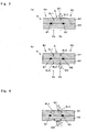
- Fig 4 is a schematic cross sectional diagram showing a bonded substrate.
- a first substrate G1 and a second substrate G2 are secured to each other by means of sealing materials S1 and S2.
- sealing materials S1 and S2 When scribe lines SL1 and SL3 are created on the first substrate G1 side using a scribing wheel W1, a force for spreading the substrate to the left and right is applied in the vicinity of the cracks created along the scribe lines SL1 and SL3.
- the rear of the first substrate G1 is secured to the second substrate by means of the sealing materials S1 and S2. Therefore, the first substrate G1 bends so that the surface becomes convex, and at the same time, as a counteraction, the second substrate G2 bends so that the surface becomes concave.
- a process for removing contraction stress is carried out on the second substrate G2 side before a scribing process is carried out on the second substrate G2.
- a substrate to be processed is a brittle material substrate having a substrate structure where a first substrate and a second substrate are bonded together with a sealing material so that a number of products are formed in locations respectively including a sealing material in the substrate structure and an end material region is formed between adjacent products
- scribe lines are created in a first and second substrate along which products are cut out using a scribing wheel through the following steps.
- a scribe line for cutting stress is created in the center of the end material region between adjacent products in the second substrate in the step (b).
- This scribe line for releasing stress is created in a different location from the scribe line for cutting of the second substrate under such conditions that the contact pressure is high.
- a scribe line for releasing stress is created in the vicinity of the center of the end material region between adjacent products in the first substrate, separately from the scribe lines to be used for cutting out a product on the first substrate side, before the step (a), after the step (a), or after the step (b).
- the scribe lines for releasing stress provided in the first substrate and the second substrate are not excellent, because horizontal cracks and cullets are caused, but they are created in such locations as not to affect the products, and thus cause no problem.
- scribe lines for releasing stress are created in the first and second substrates, so that contracting stress is released from the second substrate.
- scribe lines to be used for cutting out products on the second substrate side are created, and afterwards, scribe lines can be created under the same contact pressure conditions as for the first substrate, and the quality of processing can be kept the same as in the first substrate.
- the scribe lines for releasing stress may make cracks created by the scribe lines run deeper in the direction of the thickness of the substrate than the scribe lines used for cutting out products on the second substrate side. As a result, the contraction stress on the second substrate side can be released without failure, and good scribe lines to be used for cutting out products on the second substrate side can be created stably.
- a stable scribing process can be carried out on the surface of the substrates on both sides of a bonded substrate without the substrate being affected by contraction stress when a scribing process for cutting out products from a bonded substrate is carried out.
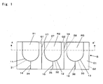
- Fig 1 is a plan diagram showing an example of a bonded substrate.
- Figs 2(a) to 2(c) are cross sectional diagrams along A-A' in Fig 1 illustrating the procedure for the scribing method according to the present invention, which can be implemented for the bonded substrate G in Fig 1 .
- the bonded substrate G is made of a first substrate G1 and a second substrate G2 which makes contact with the rear side of the first substrate G1.
- the first substrate G1 and the second substrate G2 face each other and have areas where products R1, R2 and R3 are to be created. End material regions Q1 and Q2 to be discarded after products are cut out are provided between adjacent products R1 and R2, as well as between products R2 and R3.
- the end material regions are used as a buffer region at the time of processing.
- Scribe lines are created through the following procedure when products are cut out from the bonded substrate G.
- scribe lines to be used for cutting out products R1 to R3 on the first substrate side are created in the first substrate G1.
- scribe lines for outlines 11, 12 and 13, which become outlines for the products, and auxiliary scribe lines 14, 15 and 16 (see Fig 1 ), which lead cracks to the scribe lines for outlines so as to assist cutting are created.
- These scribe lines are created in the first substrate G1 so that the substrate G bends with the first substrate G1 side convex and the second substrate G2 side concave, in such a state that contraction stress is applied on the surface of the second substrate G2.
- scribe lines for releasing stress are created in the end material region of the first substrate G1.
- linear scribe lines for releasing stress 17 and 18 are created in the vicinity of the center of the end material region provided between the products R1 and R2, as well as between the products R2 and R3, in different locations from the scribe lines for cutting out the products (vicinity of center of end material regions Q1 and Q2).
- the scribe lines for releasing stress 17 and 18 and the scribe lines for outlines 11 to 16 to be used for cutting out products may be created in the opposite order in the first substrate G1 (here, the scribe lines for releasing stress 17 and 18 may be created after the below described scribe lines for releasing stress 27 and 28 in the second substrate G2).
- scribe lines for releasing stress are created in the end material region in the second substrate G2.
- linear scribe lines for releasing stress 27 and 28 are created in such locations as to face the scribe lines for releasing stress 17 and 18 (in the vicinity of the center of the end material region Q1 and Q2 in the second substrate G2) in the vicinity of the center of the end material region provided between the products R1 and R2, as well as between the products R2 and R3.
- stronger contact stress than for creating the scribe line for outlines 11 and the like is applied.
- scribe lines to be used for cutting products R1 to R3 on the second substrate G2 side are created in the second substrate G2.
- scribe lines for outlines 31, 32 and 33 and auxiliary scribe lines 34, 35 and 36 are created.
- contraction stress is released from the second substrate G2, due to the scribe lines for releasing stress 17, 18, 27 and 28, and therefore, the scribing process can be carried out under the same contact pressure conditions as for the scribing process on the first substrate G1.
- scribe lines for releasing stress 17, 18, 27 and 28 are created after scribing the first substrate G1, and after that, the second substrate G2 is scribed, so that a scribing process can be carried out on the first substrate G1 and the second substrate G2 under the same contact pressure conditions, and the quality of the created scribe lines can be kept the same.
- the scribe lines for releasing stress 17, 18, 27 and 28 may be created from approximately 1 mm inside the end surface of each substrate (so-called inner cutting).
- the scribing method according to the present invention can be used for scribing processes for a bonded substrate.
Landscapes
- Engineering & Computer Science (AREA)
- Chemical & Material Sciences (AREA)
- Physics & Mathematics (AREA)
- Nonlinear Science (AREA)
- Mechanical Engineering (AREA)
- General Physics & Mathematics (AREA)
- Crystallography & Structural Chemistry (AREA)
- Optics & Photonics (AREA)
- Materials Engineering (AREA)
- Organic Chemistry (AREA)
- Mining & Mineral Resources (AREA)
- Re-Forming, After-Treatment, Cutting And Transporting Of Glass Products (AREA)
- Processing Of Stones Or Stones Resemblance Materials (AREA)
Applications Claiming Priority (1)
| Application Number | Priority Date | Filing Date | Title |
|---|---|---|---|
| JP2008264523A JP5192977B2 (ja) | 2008-10-10 | 2008-10-10 | 貼り合せ基板のスクライブ方法 |
Publications (2)
| Publication Number | Publication Date |
|---|---|
| EP2174762A1 EP2174762A1 (en) | 2010-04-14 |
| EP2174762B1 true EP2174762B1 (en) | 2014-08-13 |
Family
ID=41491691
Family Applications (1)
| Application Number | Title | Priority Date | Filing Date |
|---|---|---|---|
| EP09171792.6A Not-in-force EP2174762B1 (en) | 2008-10-10 | 2009-09-30 | Method for scribing bonded substrates |
Country Status (5)
| Country | Link |
|---|---|
| EP (1) | EP2174762B1 (enExample) |
| JP (1) | JP5192977B2 (enExample) |
| KR (1) | KR101054356B1 (enExample) |
| CN (1) | CN101722581B (enExample) |
| TW (1) | TW201032974A (enExample) |
Families Citing this family (9)
| Publication number | Priority date | Publication date | Assignee | Title |
|---|---|---|---|---|
| JP5156080B2 (ja) * | 2010-11-05 | 2013-03-06 | 三星ダイヤモンド工業株式会社 | 貼り合せ基板のスクライブ方法 |
| TWI462885B (zh) * | 2010-12-13 | 2014-12-01 | Mitsuboshi Diamond Ind Co Ltd | Method of breaking the substrate |
| JP5133436B2 (ja) * | 2011-03-08 | 2013-01-30 | シャープ株式会社 | 液晶パネルの製造方法 |
| JP2015034112A (ja) * | 2013-08-09 | 2015-02-19 | 三星ダイヤモンド工業株式会社 | 積層セラミックス基板の分断方法 |
| JP6243699B2 (ja) * | 2013-10-25 | 2017-12-06 | 三星ダイヤモンド工業株式会社 | 脆性材料基板の分断装置 |
| JP6432245B2 (ja) * | 2014-09-26 | 2018-12-05 | 三星ダイヤモンド工業株式会社 | 基板分断方法 |
| CN104280922B (zh) * | 2014-10-27 | 2017-05-03 | 京东方科技集团股份有限公司 | 一种液晶屏玻璃切割方法和装置 |
| CN109079909A (zh) * | 2017-06-14 | 2018-12-25 | 张家港康得新光电材料有限公司 | 利用保护膜的产品加工方法 |
| CN117283622B (zh) * | 2023-09-28 | 2025-11-14 | 广州弘亚数控机械集团股份有限公司 | 一种释放板材应力的板材切割方法、装置及存储介质 |
Family Cites Families (10)
| Publication number | Priority date | Publication date | Assignee | Title |
|---|---|---|---|---|
| JP3042192B2 (ja) * | 1992-07-29 | 2000-05-15 | 三星ダイヤモンド工業株式会社 | 貼り合せガラス基板の裁断方法及びその装置 |
| JPH11305181A (ja) * | 1998-04-17 | 1999-11-05 | Mitsubishi Electric Corp | 液晶表示パネルの切断条件設定方法 |
| JP3965902B2 (ja) * | 2000-05-23 | 2007-08-29 | 株式会社日立製作所 | 液晶表示装置の製造方法 |
| CN100361914C (zh) * | 2001-03-16 | 2008-01-16 | 三星宝石工业株式会社 | 割划方法、刀轮、使用该刀轮的割划设备和制造该刀轮的设备 |
| CN100430327C (zh) * | 2001-04-02 | 2008-11-05 | 三星钻石工业股份有限公司 | 切刀滚轮及使用该切刀滚轮的刻痕装置、刻痕方法及贴合基板的分断方法、以及制造切刀滚轮的切刀滚轮制造方法和制造装置 |
| JP4502964B2 (ja) * | 2001-04-02 | 2010-07-14 | 三星ダイヤモンド工業株式会社 | 貼り合わせ基板の分断方法 |
| TWI226877B (en) * | 2001-07-12 | 2005-01-21 | Mitsuboshi Diamond Ind Co Ltd | Method of manufacturing adhered brittle material substrates and method of separating adhered brittle material substrates |
| US20040123717A1 (en) * | 2002-04-02 | 2004-07-01 | Kazuya Maekawa | Cutter wheel, device and method using the cutter wheel, method of dividing laminated substrate, and method and device for manufacturing cutter wheel |
| EP1747867A1 (en) * | 2004-05-20 | 2007-01-31 | Mitsuboshi Diamond Industrial Co., Ltd. | Motherboard cutting method, motherboard scribing apparatus, program and recording medium |
| JP4885675B2 (ja) * | 2006-09-27 | 2012-02-29 | 株式会社Nsc | 貼合せガラス板の切断分離方法 |
-
2008
- 2008-10-10 JP JP2008264523A patent/JP5192977B2/ja not_active Expired - Fee Related
-
2009
- 2009-08-31 KR KR1020090081125A patent/KR101054356B1/ko not_active Expired - Fee Related
- 2009-09-25 CN CN2009101788069A patent/CN101722581B/zh not_active Expired - Fee Related
- 2009-09-30 EP EP09171792.6A patent/EP2174762B1/en not_active Not-in-force
- 2009-10-06 TW TW098133857A patent/TW201032974A/zh not_active IP Right Cessation
Also Published As
| Publication number | Publication date |
|---|---|
| JP2010090022A (ja) | 2010-04-22 |
| KR20100040662A (ko) | 2010-04-20 |
| KR101054356B1 (ko) | 2011-08-04 |
| JP5192977B2 (ja) | 2013-05-08 |
| EP2174762A1 (en) | 2010-04-14 |
| CN101722581B (zh) | 2012-10-17 |
| TWI357851B (enExample) | 2012-02-11 |
| CN101722581A (zh) | 2010-06-09 |
| TW201032974A (en) | 2010-09-16 |
Similar Documents
| Publication | Publication Date | Title |
|---|---|---|
| EP2174762B1 (en) | Method for scribing bonded substrates | |
| JP5542976B2 (ja) | 貼り合せ基板スクライブ加工装置 | |
| JP5185379B2 (ja) | マザー基板の基板加工方法 | |
| JP4996703B2 (ja) | 基板分断装置 | |
| TWI610893B (zh) | 貼合基板之分斷裝置 | |
| WO2005072926A1 (ja) | カッターホイールおよびこれを用いた脆性材料基板のスクライブ方法および分断方法、ならびにカッターホイールの製造方法 | |
| JP2010052995A (ja) | マザー基板のスクライブ方法 | |
| CN102036924B (zh) | 单位显示板的取出方法 | |
| TW201441168A (zh) | 基板加工系統及基板加工方法 | |
| TWI458690B (zh) | Method of breaking the substrate | |
| KR100633300B1 (ko) | 액정표시 패널의 제조방법 | |
| KR100772169B1 (ko) | 기판의 브레이크 픽업 장치 | |
| KR100943269B1 (ko) | 조립기판으로부터 액정표시패널을 분리하는 방법 | |
| JP2008083356A (ja) | 表示パネルおよび表示パネルの端縁処理方法 | |
| JPH10268276A (ja) | 液晶表示装置及びその製造方法 |
Legal Events
| Date | Code | Title | Description |
|---|---|---|---|
| PUAI | Public reference made under article 153(3) epc to a published international application that has entered the european phase |
Free format text: ORIGINAL CODE: 0009012 |
|
| 17P | Request for examination filed |
Effective date: 20090930 |
|
| AK | Designated contracting states |
Kind code of ref document: A1 Designated state(s): AT BE BG CH CY CZ DE DK EE ES FI FR GB GR HR HU IE IS IT LI LT LU LV MC MK MT NL NO PL PT RO SE SI SK SM TR |
|
| AX | Request for extension of the european patent |
Extension state: AL BA RS |
|
| GRAP | Despatch of communication of intention to grant a patent |
Free format text: ORIGINAL CODE: EPIDOSNIGR1 |
|
| INTG | Intention to grant announced |
Effective date: 20140306 |
|
| GRAS | Grant fee paid |
Free format text: ORIGINAL CODE: EPIDOSNIGR3 |
|
| GRAA | (expected) grant |
Free format text: ORIGINAL CODE: 0009210 |
|
| AK | Designated contracting states |
Kind code of ref document: B1 Designated state(s): AT BE BG CH CY CZ DE DK EE ES FI FR GB GR HR HU IE IS IT LI LT LU LV MC MK MT NL NO PL PT RO SE SI SK SM TR |
|
| REG | Reference to a national code |
Ref country code: GB Ref legal event code: FG4D |
|
| REG | Reference to a national code |
Ref country code: CH Ref legal event code: EP Ref country code: AT Ref legal event code: REF Ref document number: 681923 Country of ref document: AT Kind code of ref document: T Effective date: 20140815 |
|
| REG | Reference to a national code |
Ref country code: IE Ref legal event code: FG4D |
|
| REG | Reference to a national code |
Ref country code: DE Ref legal event code: R096 Ref document number: 602009025911 Country of ref document: DE Effective date: 20140925 |
|
| REG | Reference to a national code |
Ref country code: NL Ref legal event code: VDEP Effective date: 20140813 |
|
| REG | Reference to a national code |
Ref country code: AT Ref legal event code: MK05 Ref document number: 681923 Country of ref document: AT Kind code of ref document: T Effective date: 20140813 |
|
| REG | Reference to a national code |
Ref country code: LT Ref legal event code: MG4D |
|
| PG25 | Lapsed in a contracting state [announced via postgrant information from national office to epo] |
Ref country code: GR Free format text: LAPSE BECAUSE OF FAILURE TO SUBMIT A TRANSLATION OF THE DESCRIPTION OR TO PAY THE FEE WITHIN THE PRESCRIBED TIME-LIMIT Effective date: 20141114 Ref country code: BG Free format text: LAPSE BECAUSE OF FAILURE TO SUBMIT A TRANSLATION OF THE DESCRIPTION OR TO PAY THE FEE WITHIN THE PRESCRIBED TIME-LIMIT Effective date: 20141113 Ref country code: LT Free format text: LAPSE BECAUSE OF FAILURE TO SUBMIT A TRANSLATION OF THE DESCRIPTION OR TO PAY THE FEE WITHIN THE PRESCRIBED TIME-LIMIT Effective date: 20140813 Ref country code: ES Free format text: LAPSE BECAUSE OF FAILURE TO SUBMIT A TRANSLATION OF THE DESCRIPTION OR TO PAY THE FEE WITHIN THE PRESCRIBED TIME-LIMIT Effective date: 20140813 Ref country code: SE Free format text: LAPSE BECAUSE OF FAILURE TO SUBMIT A TRANSLATION OF THE DESCRIPTION OR TO PAY THE FEE WITHIN THE PRESCRIBED TIME-LIMIT Effective date: 20140813 Ref country code: PT Free format text: LAPSE BECAUSE OF FAILURE TO SUBMIT A TRANSLATION OF THE DESCRIPTION OR TO PAY THE FEE WITHIN THE PRESCRIBED TIME-LIMIT Effective date: 20141215 Ref country code: NO Free format text: LAPSE BECAUSE OF FAILURE TO SUBMIT A TRANSLATION OF THE DESCRIPTION OR TO PAY THE FEE WITHIN THE PRESCRIBED TIME-LIMIT Effective date: 20141113 Ref country code: FI Free format text: LAPSE BECAUSE OF FAILURE TO SUBMIT A TRANSLATION OF THE DESCRIPTION OR TO PAY THE FEE WITHIN THE PRESCRIBED TIME-LIMIT Effective date: 20140813 |
|
| PG25 | Lapsed in a contracting state [announced via postgrant information from national office to epo] |
Ref country code: AT Free format text: LAPSE BECAUSE OF FAILURE TO SUBMIT A TRANSLATION OF THE DESCRIPTION OR TO PAY THE FEE WITHIN THE PRESCRIBED TIME-LIMIT Effective date: 20140813 Ref country code: CY Free format text: LAPSE BECAUSE OF FAILURE TO SUBMIT A TRANSLATION OF THE DESCRIPTION OR TO PAY THE FEE WITHIN THE PRESCRIBED TIME-LIMIT Effective date: 20140813 Ref country code: IS Free format text: LAPSE BECAUSE OF FAILURE TO SUBMIT A TRANSLATION OF THE DESCRIPTION OR TO PAY THE FEE WITHIN THE PRESCRIBED TIME-LIMIT Effective date: 20141213 Ref country code: LV Free format text: LAPSE BECAUSE OF FAILURE TO SUBMIT A TRANSLATION OF THE DESCRIPTION OR TO PAY THE FEE WITHIN THE PRESCRIBED TIME-LIMIT Effective date: 20140813 Ref country code: HR Free format text: LAPSE BECAUSE OF FAILURE TO SUBMIT A TRANSLATION OF THE DESCRIPTION OR TO PAY THE FEE WITHIN THE PRESCRIBED TIME-LIMIT Effective date: 20140813 |
|
| PG25 | Lapsed in a contracting state [announced via postgrant information from national office to epo] |
Ref country code: NL Free format text: LAPSE BECAUSE OF FAILURE TO SUBMIT A TRANSLATION OF THE DESCRIPTION OR TO PAY THE FEE WITHIN THE PRESCRIBED TIME-LIMIT Effective date: 20140813 |
|
| REG | Reference to a national code |
Ref country code: DE Ref legal event code: R119 Ref document number: 602009025911 Country of ref document: DE |
|
| PG25 | Lapsed in a contracting state [announced via postgrant information from national office to epo] |
Ref country code: DK Free format text: LAPSE BECAUSE OF FAILURE TO SUBMIT A TRANSLATION OF THE DESCRIPTION OR TO PAY THE FEE WITHIN THE PRESCRIBED TIME-LIMIT Effective date: 20140813 Ref country code: CZ Free format text: LAPSE BECAUSE OF FAILURE TO SUBMIT A TRANSLATION OF THE DESCRIPTION OR TO PAY THE FEE WITHIN THE PRESCRIBED TIME-LIMIT Effective date: 20140813 Ref country code: SK Free format text: LAPSE BECAUSE OF FAILURE TO SUBMIT A TRANSLATION OF THE DESCRIPTION OR TO PAY THE FEE WITHIN THE PRESCRIBED TIME-LIMIT Effective date: 20140813 Ref country code: RO Free format text: LAPSE BECAUSE OF FAILURE TO SUBMIT A TRANSLATION OF THE DESCRIPTION OR TO PAY THE FEE WITHIN THE PRESCRIBED TIME-LIMIT Effective date: 20140813 Ref country code: IT Free format text: LAPSE BECAUSE OF FAILURE TO SUBMIT A TRANSLATION OF THE DESCRIPTION OR TO PAY THE FEE WITHIN THE PRESCRIBED TIME-LIMIT Effective date: 20140813 Ref country code: EE Free format text: LAPSE BECAUSE OF FAILURE TO SUBMIT A TRANSLATION OF THE DESCRIPTION OR TO PAY THE FEE WITHIN THE PRESCRIBED TIME-LIMIT Effective date: 20140813 |
|
| REG | Reference to a national code |
Ref country code: CH Ref legal event code: PL |
|
| PG25 | Lapsed in a contracting state [announced via postgrant information from national office to epo] |
Ref country code: MC Free format text: LAPSE BECAUSE OF FAILURE TO SUBMIT A TRANSLATION OF THE DESCRIPTION OR TO PAY THE FEE WITHIN THE PRESCRIBED TIME-LIMIT Effective date: 20140813 Ref country code: PL Free format text: LAPSE BECAUSE OF FAILURE TO SUBMIT A TRANSLATION OF THE DESCRIPTION OR TO PAY THE FEE WITHIN THE PRESCRIBED TIME-LIMIT Effective date: 20140813 |
|
| PLBE | No opposition filed within time limit |
Free format text: ORIGINAL CODE: 0009261 |
|
| STAA | Information on the status of an ep patent application or granted ep patent |
Free format text: STATUS: NO OPPOSITION FILED WITHIN TIME LIMIT |
|
| REG | Reference to a national code |
Ref country code: DE Ref legal event code: R119 Ref document number: 602009025911 Country of ref document: DE Effective date: 20150401 |
|
| REG | Reference to a national code |
Ref country code: FR Ref legal event code: ST Effective date: 20150529 |
|
| PG25 | Lapsed in a contracting state [announced via postgrant information from national office to epo] |
Ref country code: BE Free format text: LAPSE BECAUSE OF NON-PAYMENT OF DUE FEES Effective date: 20140930 |
|
| REG | Reference to a national code |
Ref country code: IE Ref legal event code: MM4A |
|
| 26N | No opposition filed |
Effective date: 20150515 |
|
| GBPC | Gb: european patent ceased through non-payment of renewal fee |
Effective date: 20141113 |
|
| PG25 | Lapsed in a contracting state [announced via postgrant information from national office to epo] |
Ref country code: LI Free format text: LAPSE BECAUSE OF NON-PAYMENT OF DUE FEES Effective date: 20140930 Ref country code: CH Free format text: LAPSE BECAUSE OF NON-PAYMENT OF DUE FEES Effective date: 20140930 Ref country code: DE Free format text: LAPSE BECAUSE OF NON-PAYMENT OF DUE FEES Effective date: 20150401 |
|
| PG25 | Lapsed in a contracting state [announced via postgrant information from national office to epo] |
Ref country code: IE Free format text: LAPSE BECAUSE OF NON-PAYMENT OF DUE FEES Effective date: 20140930 Ref country code: FR Free format text: LAPSE BECAUSE OF NON-PAYMENT OF DUE FEES Effective date: 20141013 |
|
| PG25 | Lapsed in a contracting state [announced via postgrant information from national office to epo] |
Ref country code: GB Free format text: LAPSE BECAUSE OF NON-PAYMENT OF DUE FEES Effective date: 20141113 |
|
| PG25 | Lapsed in a contracting state [announced via postgrant information from national office to epo] |
Ref country code: SI Free format text: LAPSE BECAUSE OF FAILURE TO SUBMIT A TRANSLATION OF THE DESCRIPTION OR TO PAY THE FEE WITHIN THE PRESCRIBED TIME-LIMIT Effective date: 20140813 |
|
| PG25 | Lapsed in a contracting state [announced via postgrant information from national office to epo] |
Ref country code: SM Free format text: LAPSE BECAUSE OF FAILURE TO SUBMIT A TRANSLATION OF THE DESCRIPTION OR TO PAY THE FEE WITHIN THE PRESCRIBED TIME-LIMIT Effective date: 20140813 |
|
| PG25 | Lapsed in a contracting state [announced via postgrant information from national office to epo] |
Ref country code: MT Free format text: LAPSE BECAUSE OF FAILURE TO SUBMIT A TRANSLATION OF THE DESCRIPTION OR TO PAY THE FEE WITHIN THE PRESCRIBED TIME-LIMIT Effective date: 20140813 |
|
| PG25 | Lapsed in a contracting state [announced via postgrant information from national office to epo] |
Ref country code: LU Free format text: LAPSE BECAUSE OF NON-PAYMENT OF DUE FEES Effective date: 20140930 Ref country code: HU Free format text: LAPSE BECAUSE OF FAILURE TO SUBMIT A TRANSLATION OF THE DESCRIPTION OR TO PAY THE FEE WITHIN THE PRESCRIBED TIME-LIMIT; INVALID AB INITIO Effective date: 20090930 Ref country code: TR Free format text: LAPSE BECAUSE OF FAILURE TO SUBMIT A TRANSLATION OF THE DESCRIPTION OR TO PAY THE FEE WITHIN THE PRESCRIBED TIME-LIMIT Effective date: 20140813 Ref country code: BE Free format text: LAPSE BECAUSE OF FAILURE TO SUBMIT A TRANSLATION OF THE DESCRIPTION OR TO PAY THE FEE WITHIN THE PRESCRIBED TIME-LIMIT Effective date: 20140813 |
|
| PG25 | Lapsed in a contracting state [announced via postgrant information from national office to epo] |
Ref country code: MK Free format text: LAPSE BECAUSE OF FAILURE TO SUBMIT A TRANSLATION OF THE DESCRIPTION OR TO PAY THE FEE WITHIN THE PRESCRIBED TIME-LIMIT Effective date: 20140813 |