EP2172878A2 - Verfahren zur Herstellung von RFID-Etiketten und RFID-Etiketten - Google Patents
Verfahren zur Herstellung von RFID-Etiketten und RFID-Etiketten Download PDFInfo
- Publication number
- EP2172878A2 EP2172878A2 EP09171507A EP09171507A EP2172878A2 EP 2172878 A2 EP2172878 A2 EP 2172878A2 EP 09171507 A EP09171507 A EP 09171507A EP 09171507 A EP09171507 A EP 09171507A EP 2172878 A2 EP2172878 A2 EP 2172878A2
- Authority
- EP
- European Patent Office
- Prior art keywords
- sheet member
- sheet
- members
- reinforcing
- rfid
- Prior art date
- Legal status (The legal status is an assumption and is not a legal conclusion. Google has not performed a legal analysis and makes no representation as to the accuracy of the status listed.)
- Granted
Links
Images












Classifications
-
- G—PHYSICS
- G06—COMPUTING OR CALCULATING; COUNTING
- G06K—GRAPHICAL DATA READING; PRESENTATION OF DATA; RECORD CARRIERS; HANDLING RECORD CARRIERS
- G06K19/00—Record carriers for use with machines and with at least a part designed to carry digital markings
- G06K19/06—Record carriers for use with machines and with at least a part designed to carry digital markings characterised by the kind of the digital marking, e.g. shape, nature, code
- G06K19/067—Record carriers with conductive marks, printed circuits or semiconductor circuit elements, e.g. credit or identity cards also with resonating or responding marks without active components
- G06K19/07—Record carriers with conductive marks, printed circuits or semiconductor circuit elements, e.g. credit or identity cards also with resonating or responding marks without active components with integrated circuit chips
-
- G—PHYSICS
- G06—COMPUTING OR CALCULATING; COUNTING
- G06K—GRAPHICAL DATA READING; PRESENTATION OF DATA; RECORD CARRIERS; HANDLING RECORD CARRIERS
- G06K19/00—Record carriers for use with machines and with at least a part designed to carry digital markings
- G06K19/06—Record carriers for use with machines and with at least a part designed to carry digital markings characterised by the kind of the digital marking, e.g. shape, nature, code
- G06K19/067—Record carriers with conductive marks, printed circuits or semiconductor circuit elements, e.g. credit or identity cards also with resonating or responding marks without active components
- G06K19/07—Record carriers with conductive marks, printed circuits or semiconductor circuit elements, e.g. credit or identity cards also with resonating or responding marks without active components with integrated circuit chips
- G06K19/077—Constructional details, e.g. mounting of circuits in the carrier
- G06K19/07749—Constructional details, e.g. mounting of circuits in the carrier the record carrier being capable of non-contact communication, e.g. constructional details of the antenna of a non-contact smart card
-
- G—PHYSICS
- G06—COMPUTING OR CALCULATING; COUNTING
- G06K—GRAPHICAL DATA READING; PRESENTATION OF DATA; RECORD CARRIERS; HANDLING RECORD CARRIERS
- G06K19/00—Record carriers for use with machines and with at least a part designed to carry digital markings
- G06K19/06—Record carriers for use with machines and with at least a part designed to carry digital markings characterised by the kind of the digital marking, e.g. shape, nature, code
- G06K19/067—Record carriers with conductive marks, printed circuits or semiconductor circuit elements, e.g. credit or identity cards also with resonating or responding marks without active components
- G06K19/07—Record carriers with conductive marks, printed circuits or semiconductor circuit elements, e.g. credit or identity cards also with resonating or responding marks without active components with integrated circuit chips
- G06K19/077—Constructional details, e.g. mounting of circuits in the carrier
- G06K19/07718—Constructional details, e.g. mounting of circuits in the carrier the record carrier being manufactured in a continuous process, e.g. using endless rolls
-
- Y—GENERAL TAGGING OF NEW TECHNOLOGICAL DEVELOPMENTS; GENERAL TAGGING OF CROSS-SECTIONAL TECHNOLOGIES SPANNING OVER SEVERAL SECTIONS OF THE IPC; TECHNICAL SUBJECTS COVERED BY FORMER USPC CROSS-REFERENCE ART COLLECTIONS [XRACs] AND DIGESTS
- Y10—TECHNICAL SUBJECTS COVERED BY FORMER USPC
- Y10T—TECHNICAL SUBJECTS COVERED BY FORMER US CLASSIFICATION
- Y10T29/00—Metal working
- Y10T29/49—Method of mechanical manufacture
- Y10T29/49002—Electrical device making
- Y10T29/49016—Antenna or wave energy "plumbing" making
Definitions
- a sheet-like substrate itself which is formed with antenna patterns in advance, can be prepared with such a small thickness that enables the same to be wound around a roll or the like.
- both the IC chip and the reinforcing members have large bending resistances, which makes it difficult to cause the sheet-like substrate to be taken up by a roll again. Therefore, for example, a sealing process using a protective sheet is required to be performed by batch processing after the sheet-like substrate is cut in units of one or a plurality of IC chips.
- a sealing process using a protective sheet is required to be performed by batch processing after the sheet-like substrate is cut in units of one or a plurality of IC chips.
- the sheet members 12 and 13 form an upper sheet member 14 which is laminated on the sheet member 11, and a reinforcing member 23 for reinforcing the IC chip 21 is disposed between the sheet members 12 and 13 at a location corresponding to the IC chip 21.
- the reinforcing member 23 is completely sealed with the sheet members 12 and 13.
- the reinforcing member 23 is disposed only above the IC chip 21, it is possible to dispose the same reinforcing member also below the IC chip 21. In this case, it suffices that with a reinforcing member attached to a lower surface of the sheet member 11, another sheet member is laminated thereon in a manner sandwiching the reinforcing member, and is fixedly attached to the sheet member 11. In this case, however, at least one of the sheet member 11 and the sheet member provided thereunder is formed in advance using an elastic material.
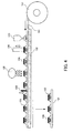
- the antenna substrate 101 formed with the antenna patterns 102, as described above, is provided in a state wound around a roll 121.
- the antenna substrate 101 is sequentially pulled out onto a stage 122, and the IC chips 103 are sequentially mounted to the antenna substrate 101 on the stage 122.
- the IC chips 103 are mounted e.g. by flip chip bonding using a bonding tool 123.
- Each IC chip 103 has a lower surface or a side surface formed with two antenna terminals, not illustrated, and these antenna terminals are connected to respective portions of each antenna pattern 102, separated by the gap.
- the antenna substrate 101 having the IC chips 103 mounted through the above-described process step are taken up by the roll again.
- FIG. 4 explains a process step for mounting the reinforcing members on the antenna substrate 101 in the general RFID tag-manufacturing process.
- an adhesive agent is applied to the IC chips 103 on the antenna substrate 101 by a dispenser 133.
- the reinforcing members 104 are placed on the upper surfaces of the IC chips 103 coated with the adhesive agent, by a bonding tool 134, and further the adhesive agent is cured by heat from a heat source 135.
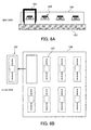
- FIGS. 5A and 5B explain a process step for cutting out RFID inlets in the general RFID tag-manufacturing process.
- FIG. 5A is a side view illustrating how this process step is carried out
- FIG. 5B is a plan view illustrating the same.
- the antenna substrate 101 cut as described above is punched by a punching die 142 along dotted lines in FIG. 5B , whereby a group of electronic components constituting an RFID tag are packaged whereby an RFID inlet 105 is formed.
- the RFID units 107 in each of which the whole of the RFID inlet 105 having the IC chip 103 and the antenna pattern 102 reinforced by the reinforcing member 104 mounted thereon is sealed with the protective sheet 106.
- the RFID unit 107 is resistant to external forces, such as a bending force and a pressing force, and at the same time even when the RFID unit 107 is placed in a liquid or a chemical, the inside of the RFID unit 107 is prevented from being corroded.
- the antenna pattern is linearly formed, it is possible to use an antenna pattern having a loop-like or spiral-like shape.
- FIG. 9 is a flowchart illustrating the outline of a process for manufacturing RFID units according to a second embodiment.
- an antenna substrate formed with an antenna pattern is prepared by the same method as used in the above-described general RFID tag-manufacturing process.
- the prepared antenna substrate is taken up by a roll.
- Step S23 IC chips are mounted on the antenna substrate by the same method as used in the above-described general RFID tag-manufacturing process.
- the antenna substrate having the IC chips mounted thereon can also be taken up by a roll.
- Step S24 Slits are formed in respective predetermined locations of the antenna substrate having the IC chips mounted thereon.
- the antenna substrate formed with the slits is taken up by a roll.
- Step S25 The antenna substrate having the slits formed in the step S24 is sandwiched from opposite sides by the sheet laminates prepared in the step S21, and the sheet laminates are fixedly attached to each other. Further, the member formed by fixedly attaching the sheet laminates is cut out in units of regions of respective RFID tags to thereby complete RFID units. In this process step, by pulling out the antenna substrate and the sheet laminates from the respective rolls thereof at the same speed, it is possible to fixedly attach the sheet laminates to each other and further cut out the RFID units.
- FIGS. 10A and 10B explain a sheet laminate-preparing process step according to the second embodiment.
- FIG. 10A is a side view illustrating how this process step is carried out
- FIG. 10B is a plan view illustrating the same.
- the process step illustrated in FIGS. 10A and 10B corresponds to the step S21 in FIG. 9 .
- a sheet-like nylon mesh 201 and rubber sheets 202a and 202b are provided in states wound around rolls 221, 222a and 222b, respectively, and a sheet laminate is prepared by laminating the sheet-like nylon mesh 201 and the rubber sheets 202a and 202b.
- the nylon mesh 201 is used as a reinforcing member for noncontact IC chips, and has a width at least large enough to cover the whole of each IC chip.
- the material for the reinforcing member is not limited to nylon but any of resin materials and metal materials, including metal nets, may be used as the material for the reinforcing member insofar as it is in the form of a mesh. However, it is desirable that the material has a certain degree of rigidity, and is difficult to extend and at the same time bendable to a certain degree. Further, to maintain an excellent communication performance of the IC chips, it is desirable that the material is non-conductive.
- the nylon mesh 201 and the rubber sheets 202a and 202b are pulled in between rollers 223a and 223b from the rolls 221, 222a and 222b, and are laminated one upon another. At this time, the nylon mesh 201 is vertically sandwiched between the rubber sheets 202a and 202b, and the resulting laminate is taken up by a roll 224.
- the nylon mesh 201 it is not particularly necessary to attach the nylon mesh 201 to the laminated rubber sheets 202a and 202b.
- the opposite surfaces of the nylon mesh 201, or respective surfaces of the rubber sheets 202a and 202b, opposed to the nylon mesh 201 are coated with an adhesive agent such that the opposed surfaces thereof are attached to each other.
- the antenna substrate formed with the antenna pattern is prepared, separately from the sheet laminate.
- the IC chips are mounted on the prepared antenna substrate.
- This process step is the same as the IC chip-mounting process step in the general RFID tag-manufacturing process, described above with reference to FIGS. 3A and 3B , and illustration thereof is omitted. It is assumed here that an antenna substrate 203, antenna patterns 204 and IC chips 205 illustrated in FIGS. 11A and 11B correspond to the antenna substrate 101, the antenna patterns 102 and the IC chips 103 illustrated in FIGS. 11A and 11B , respectively.
- the antenna substrate 203 having the IC chips 205 mounted thereon is once taken up e.g. by a roll 231, and then is subjected to the slit-forming process step illustrated in FIGS. 11A and 11B .
- the size of the IC chips 205 is small e.g. with respect to the width of the antenna substrate 203, and further the height thereof is low with respect to the height of e.g. the above-described reinforcing members 104, so that the antenna substrate 203 having only the IC chips 205 mounted thereon can be relatively easily wound around the roll 231.
- slits are formed in the antenna substrate 203 using a punching die 233 while the roll 231 is rotated to sequentially pull out the antenna substrate 203 onto a stage 232.
- slits 203a are formed in regions between the antenna patterns 204 arranged in parallel with each other, and slits 203b are formed in regions on the opposite longitudinal ends of each antenna pattern 204.
- these slits are formed to bring rubber sheets on opposite ends of the antenna substrate 203 into contact with each other and cause them to be fixedly attached to each other by thermocompression bonding in a sheet-attaching process step, described hereinafter. Therefore, the size of the slits and locations for forming the slits are determined such that a sufficient attaching force is caused by thermocompression bonding. Further, basically, the regions for forming the slits are not limited insofar as they do not include the IC chips 205 and the antenna patterns 204. However, as described hereinafter, the size of a portion of the antenna substrate 203, exposed from a side surface of a completed RFID unit can be reduced depending on the locations where the slits are formed and the size of the slits.
- FIGS. 12A and 12B explain a sheet-attaching/unit-cutting process step according to the second embodiment.
- FIG. 12A is a side view illustrating how this process step is carried out
- FIG. 12B is a plan view illustrating the same.
- the process step illustrated in FIGS. 12A and 12B corresponds to the step S25 in FIG. 9 .
- sheet laminates 206a and 206b formed in the step S21, respectively are arranged on opposite surfaces of the antenna substrate 203 having the slits formed in the step S24.
- the antenna substrate 203 and the sheet laminates 206a and 206b are pulled out from rolls 241, 242a and 242b, respectively, and are conveyed while being vertically pressurized by rollers 243a and 243b.
- heat is applied e.g. by the rollers 243a and 243b, or from a heat source, not illustrated, other than the rollers 243a and 243b.
- a rubber sheet as a lower layer of the sheet laminate 206a i.e. on a side opposed to the antenna substrate 203 and a rubber sheet as an upper layer of the sheet laminate 206b are thermocompression-bonded to each other via the slits formed in the antenna substrate 203, whereby the IC chips 205 and the antenna patterns 204 are sealed with the rubber sheets.
- a rubber sheet as an upper layer of the sheet laminate 206a and the rubber sheet as the lower layer of the sheet laminate 206a are thermocompression-bonded to each other via gaps of the nylon mesh 201 between the rubber sheets.
- the rubber sheet as the upper layer of the sheet laminate 206b and a rubber sheet as a lower layer of the sheet laminate 206b are thermocompression-bonded to each other via gaps of the nylon mesh 201 between the rubber sheets.
- the rubber sheet as the lower layer of the sheet laminate 206a has elastic properties, so that when press-fitted into the antenna substrate 203, the rubber sheet is contracted only by the height of the IC chip 205. This holds the upper surface of the sheet laminate 206a approximately flat.
- recesses may be formed in advance in the rubber sheet e.g. according to the shape of the IC chip 205. However, in this case, in the process step for fixedly attaching the sheet laminates 206a and 206b that have the antenna substrate 203 therebetween, it is possible to position the recesses on the sheet laminate 206a to the locations of the IC chips 205.
- the sheet members thermocompression-bonded to each other as described above are cut out by a punching die 244 in units of regions each including one IC chip 205 and one antenna pattern 204 connected to the IC chip 205.
- the units cut out in this process step become RFID units, which are final products.
- the regions cut out by the punching die 244 are indicated as cut-out regions 207.
- the cut-out regions 207 are configured to pass through the insides of the respective slits 203a and 203b formed in the antenna substrate 203.
- the sheet laminates 206a and 206b prepared in advance in the step S21 are subjected to the step S25.
- the laminating and fixedly attaching of each of the sheet laminates 206a and 206b may be performed simultaneously with the laminating and fixedly attaching of the sheet laminates 206a and 206b and the antenna substrate 203.
- FIGS. 13A and 13B illustrate the RFID unit made in the second embodiment.
- FIG. 13A is a plan view illustrating the same
- FIG. 13B is a side view illustrating the same.
- the layers of the nylon mesh 201 are formed above and below the IC chip 205. Therefore, even when pressure or a bending force is applied to the RFID unit from the outside, the IC chip 205 is protected.
- the reinforcing effects of the nylon mesh 201 will be described in more detail with reference to FIGS. 14A and 14B .
- end faces of the antenna substrate 203 are partially exposed from the side surface of the RFID unit. Therefore, it is desirable to determine the locations and size of the slits formed in the antenna substrate 203 before being cut, and the respective locations of regions from which the RFID units are cut out, such that the exposed portion of the antenna substrate 203 is minimized.
- the cut-out regions 207 are configured to pass through the insides of the respective slits 203a and 203b formed in the antenna substrate 203.
- the portion of the antenna substrate 203, exposed from the side surface of each RFID unit becomes only a region located between the slit 203a and the slit 203b adjacent to the slit 203a.
- this region is indicated as an exposed region 208.
- the antenna substrate 203 in the antenna substrate 203 yet to be cut, it is desirable to maximize the length of the slits 203a disposed between the antenna patterns 204 arranged side by side, in a direction parallel to each antenna pattern 204 (left-right direction in FIGS. 13A and 13B ).
- the width of the antenna substrate 203 may be made smaller than the width of the sheet laminates 206a and 206b, while the length of the cut-out region 207 in the direction of the width thereof may be made larger than the width of the antenna substrate 203.
- the slits 203b are not formed, and the opposite ends of the antenna substrate 203 in the direction of the length of the antenna pattern 204 are prevented from being exposed from the opposite ends of the RFID unit.
- FIGS. 14A and 14B explain the reinforcing effects of the nylon mesh.
- FIG. 14A illustrates the cross-section of a protective member used in the above-described RFID unit, i.e. a rubber sheet.
- a protective member used in the above-described RFID unit i.e. a rubber sheet.
- the layers of the nylon mesh 201 are formed above and below the IC chip 205.
- nylon meshes 201 having a low elongation are used, as illustrated in FIG. 14B , if the RFID unit is bent such that an upper half thereof, as viewed in FIG. 14A , becomes convex, an upper nylon mesh 201 is less elongated, whereby the rubber sheet in the region of the upper nylon mesh 201 is difficult to be bent.
- the RFID unit is bent such that a lower half thereof, as viewed in FIG.
- the process step is employed in which a mesh-like material is used for making reinforcing members of the IC chips, and sheet laminates are prepared by arranging the mesh-like reinforcing members on a protective sheet member.
- a mesh-like material is used for making reinforcing members of the IC chips
- sheet laminates are prepared by arranging the mesh-like reinforcing members on a protective sheet member.
- an elastic material is used as the protective sheet member, whereby when the sheet laminates and the antenna substrate are fixedly attached, it is possible to make flat the upper surface of the sheet laminate without performing particular positioning (of the sheet laminates and the IC chips) in the conveying direction of the sheet laminates and the antenna substrate. This makes it possible to manufacture a large number of RFID units, which are resistant to external forces, liquids or chemicals, at low costs.
- the RFID unit manufactured in the above-described second embodiment is configured such that part of the reinforcing members or the antenna substrate is exposed from the side surface of the RFID unit.
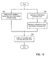
- FIG. 15 is a flowchart illustrating the outline of a process for manufacturing RFID units according to the third embodiment.
- Step S31 the same reinforcing members as used in the above-described general RFID tag-manufacturing process are used.
- the reinforcing members are mounted on protective sheet members, which serve as exteriors.
- sprocket holes for use in positioning in later process steps are formed in advance.
- the protective sheet members having the reinforcing members mounted thereon are taken up by respective rolls.
- Step S32 On the other hand, noncontact IC chips are mounted on the above-described antenna substrate, and the antenna substrate is cut in units of the IC chip and the antenna pattern, whereby RFID inlets are prepared.
- Step S33 The RFID inlets are mounted on a sheet member, which serves as an intermediate layer. At this time, sprocket holes for use in positioning in later process steps are formed in advance in the sheet member.
- the sheet member having the RFID inlets mounted thereon are taken up by a roll.
- Step S34 The protective sheet members that have the reinforcing members mounted thereon and are to form an uppermost layer and a lowermost layer, respectively, the sheet member having the RFID inlets mounted thereon, and a sheet member serving as a spacer are laminated one upon another, and are fixedly attached to each other. Further, the members fixedly attached are cut out in units of respective regions of the RFID tags, whereby RFID units are completed. In this process step, by pulling out all the sheet members from the respective rolls thereof at the same speed, it is possible to fixedly attach the sheet members to each other and then cut out the RFID units.
- FIGS. 16A and 16B explain a reinforcing member-mounting/hole-machining process step.
- FIG. 16A is a side view illustrating how this process step is carried out
- FIG. 16B is a plan view illustrating the same.
- the process step illustrated in FIGS. 16A and 16B corresponds to the step S31 in FIG. 15 .
- a rubber sheet 301 which is a protective sheet member, is provided in a state wound around a roll 331.
- This protective sheet member forms the exterior of the RFID unit as a final product, and has the function of sealing the IC chip, the antenna pattern, the reinforcing members, and so forth, within each RFID unit. It suffices that this protective sheet member is made of the same material as that of the protective sheet members arranged on the nylon mesh 201 in the first embodiment.
- the rubber sheet 301 is pulled out from the roll 331 onto a stage 332, and reinforcing members 302 of the IC chips are mounted on an upper surface of the rubber sheet 301 at predetermined space intervals P, by a mounting tool 333.
- the reinforcing members 302 there are used ones made of the same material and having the same shape as that of the reinforcing members 104 used in the aforementioned general RFID tag-manufacturing process.
- an adhesive agent 303 is attached to a lower surface of each reinforcing member 302.
- a double-faced tape is affixed as the adhesive agent 303 to the lower surface of the reinforcing member 302, by way of example.
- the reinforcing members 302 as described above are conveyed to predetermined positions on the rubber sheet 301 and are pressed against the rubber sheet 301, by the mounting tool 333. Alternatively, after the adhesive agent 303 is attached to the rubber sheet 301, the reinforcing member 302 may be affixed thereto.
- positioning sprocket holes 304 are formed by a hole-making tool 334 at predetermined space intervals through the rubber sheet 301. It suffices that the space intervals at which the sprocket holes 304 are formed are equal to space intervals P at which the reinforcing members 302 are mounted.
- the rubber sheet 301 which has the reinforcing members 302 mounted thereon and the sprocket holes 304 formed therethrough by the above process step, is taken up by a roll again.
- this roll there may be used the original roll 331 around which the rubber sheet 301 has been wound, or another roll provided on the side of the other end of the rubber sheet 301.
- FIGS. 17A and 17B explain an RFID inlet-preparing process step.
- FIG. 17A is a side view illustrating how this process step is carried out
- FIG. 17B is a plan view illustrating the same.
- the process step illustrated in FIGS. 17A and 17B corresponds to the step S32 in FIG. 15 .
- this process step first, noncontact IC chips 312 are mounted on a antenna substrate 311 by the same procedure as employed in the IC chip-mounting process step in the general RFID tag-manufacturing process, described above with reference to FIGS. 3A and 3B . More specifically, as illustrated in FIGS. 17A and 17B , the antenna substrate 311 formed with antenna patterns 313 is pulled out from a roll 341 onto a stage 342. Then, the IC chips 312 are mounted on the antenna substrate 311 e.g. by flip chip bonding using a bonding tool 343, and terminals of the IC chips 312 are connected to associated ones of the antenna patterns 313.
- the materials and shapes of the antenna substrate 311 and the antenna patterns 313 may be the same as employed in the above-described general RFID tag-manufacturing process.
- a region corresponding to a pair of one IC chip 312 and one antenna pattern 313 is punched by a punching die 344 along dotted lines in FIG. 17B , whereby a group of electronic components constituting an RFID tag is packaged, whereby the RFID inlet is prepared.
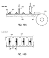
- FIGS. 18A and 18B explain an RFID inlet-mounting/hole-machining process step.
- FIG. 18A is a side view illustrating how this process step is carried out
- FIG. 18B is a plan view illustrating the same.
- the process step illustrated in FIGS. 18A and 18B corresponds to the step S33 in FIG. 15 .
- the RFID inlets prepared in the step S32 are mounted on a sheet member which serves as an intermediate layer of the RFID units.
- a rubber sheet 321 is used as the sheet member. It suffices that as the material of this sheet member, the same material as that of the protective sheet member serving as the exterior of the RFID unit may be used.
- the rubber sheet 321 is provided in a state wound around a roll 351.
- RFID inlets 322 are mounted on an upper surface of the rubber sheet 321 at predetermined space intervals, by a mounting tool 353.
- the RFID inlets 322 are mounted on the rubber sheet 321 at the same space intervals as the space intervals P at which the reinforcing members 302 are mounted on the rubber sheet 301 in the step S31.
- an adhesive agent 323 is applied to a lower surface of each RFID inlet 322.
- a double-faced tape is affixed to the lower surface of the RFID inlet 322 as the adhesive agent 323, by way of example.
- the RFID inlets 322 as described above are conveyed to predetermined positions on the rubber sheet 321, pressed against the rubber sheet 321, and affixed thereto, by the mounting tool 353.
- the RFID inlets 322 may be affixed to the adhesive agent 323.
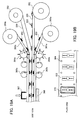
- FIGS. 19A and 19B explain a sheet-attaching/unit-cutting process step.
- FIG. 19A is a side view illustrating how this process step is carried out
- FIG. 19B is a plan view illustrating the same.
- the process step illustrated in FIGS. 19A and 19B corresponds to the step S34 in FIG. 15 .
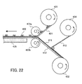
- a rubber sheet 301a having the reinforcing members 302 mounted thereon in the step S31 is laminated to a lower side of the rubber sheet 321 having the RFID inlets 322 mounted thereon in the step S33.
- a rubber sheet 301b having the reinforcing members 302 mounted thereon in the step S31 is laminated, with a spacer sheet 330 provided between the rubber sheet 321 and the rubber sheet 301b.
- the rubber sheets 301a and 301b are arranged with the reinforcing members 302 mounted thereon facing inward, respectively.
- the spacer sheet 330 is a sheet member formed of the same material as that of the rubber sheets 301a, 301b and 321. Let it be assumed that the spacer sheet 330 has sprocket holes formed at the same space intervals as the space intervals at which the sprocket holes are formed through the rubber sheets 301a, 301b and 321.
- the rubber sheets 301a, 301b and 321 and the spacer sheet 330 are pulled out from rolls 361a, 361b, 362 and 363, respectively, and are conveyed to a location between sprocket wheels 364a and 364b.
- the sprocket wheels 364a and 364b have protrusions formed on outer peripheral surfaces thereof at the same space intervals, and the rubber sheets 301a, 301b and 321 and the spacer sheet 330 are conveyed while the above protrusions are sequentially inserted into sprocket holes formed in the rubber sheets 301a, 301b and 321 and the spacer sheet 330, respectively.
- This positions the IC chips and the reinforcing members 302 such that the reinforcing members 302 mounted on the rubber sheets 301a and 301b, respectively, are accurately arranged above and below the IC chips mounted on the rubber sheet 321.
- rollers 365a and 365b are provided on downstream sides of the respective sprocket wheels 364a and 364b, and the rubber sheets 301a, 301b and 321 and the spacer sheet 330 are conveyed while being vertically pressurized by the rollers 365a and 365b.
- the rubber sheets 301a, 301b and 321 and the spacer sheet 330 are heated by the rollers 365a and 365b or by heat sources, not illustrated, other than the rollers 365a and 365b. This causes the adjacent sheets to be fixedly attached to each other by thermocompression bonding, whereby the RFID inlets 322 and the reinforcing members 302 are sealed.
- the sheets laminated one upon another particularly the rubber sheet 321 and the spacer sheet 330 have elastic properties, and hence when the sheet members are heated by the rollers 365a and 365b, regions of the respective sheet members, brought into contact with the RFID inlets 322 and the reinforcing members 302, are contracted only by the heights of the RFID inlets 105 and the reinforcing members 302. This holds the upper surface of the whole sheet laminate approximately flat.
- recesses may be formed in advance in the rubber sheet 321 and the spacer sheet 330 in accordance with the shapes of the RFID inlets 322 and the reinforcing members 302.
- the sheet members thermocompression-bonded to each other as described above are cut out on a stage 366 by a punching die 367 in units of regions each including one RFID inlet 105.
- the units cut out in this process step become RFID units, which are final products.
- the region cut out by the punching die 367 is indicated as a cut-out region 370.
- Each cut-out region 370 is configured to be larger in area than the region of the RFID inlet 105 and the reinforcing members 302 associated therewith, whereby the RFID inlet 105 and the reinforcing member 302 are completely sealed with the upper and lower sheet members.
- the sprocket holes are provided in the respective sheet members so as to position the RFID inlets 105 and the reinforcing members 302 during lamination of the sheet members, this is not limitative, but instead of such hole-like members, positioning cutouts may be provided in the lateral side portions of the sheet members. In this case, it suffices that in the lamination process step, the sheet members are conveyed with members, which correspond to the protrusions of the sprocket wheels, engaged with the cutouts of the sheet members. Further, any other suitable positioning method may be employed.
- all of the rubber sheets 301a, 301b and 321 and the spacer sheet 330 are laminated one upon another at a time.
- a procedure may be employed in which adjacent ones of the sheet members are laminated in advance, and e.g. after taking up the sheet laminates by respective rolls, all the sheet members are finally laminated one upon another.
- the sheet members may be fixedly attached each time the adjacent ones of the sheet members are laminated one upon another, when the final lamination process step is executed.
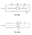
- FIGS. 20A and 20B illustrate an RFID unit prepared according to a third embodiment.
- FIG. 20A is a plan view illustrating the same, and
- FIG. 20B is a side view illustrating the same.
- the reinforcing members 302 are disposed above and below the IC chip 312 mounted on the RFID inlet 105, respectively.
- a hard material can be used for the reinforcing member 302, as described hereinabove, so that it is possible to enhance the strength of the RFID unit compared with the case where a mesh-like material is used as in the second embodiment.
- the IC chip 312, the antenna pattern 313 and the antenna substrate 311 are all sealed within protective sheet members such that they are not exposed from the outer surfaces of the RFID unit. As a consequence, even when a liquid or a chemical is attached to the RFID unit, it is possible to prevent the liquid or the chemical from touching the IC chip 312 and the antenna pattern 313 within the RFID unit, thereby making it possible to cause the IC chip 312 to normally operate. Further, since the reinforcing members 302 as well are completely sealed within the protective sheet members, it is also possible to prevent the reinforcing members 302 from being corroded.
- the RFID units it is possible to manufacture the RFID units from start to finish, by using rolls. Further, since a material that can be thermocompression-bonded is used for the protective sheet members, it is possible to efficiently carry out the process step for laminating the protective sheet members and fixedly attaching the same. Furthermore, the positioning holes are formed through the laminated protective sheet members, whereby when the protective sheet members are laminated and fixedly attached to each other, it is possible to easily position the IC chips and the reinforcing members. This makes it possible to mass-produce the RFID units having the above-mentioned features, at low costs.
- the RFID unit may be configured such that the reinforcing member 302 is disposed only above the IC chip 312.
- the arranging and fixedly attaching of the rubber sheet 301a below the IC chip 312 is omitted. That is, in this case, the rubber sheet 321 functions as a protective sheet, as an exterior, which protects the RFID inlet 322.
- part of the manufacturing process according to the second embodiment is replaced by part based on another method. More specifically, the method of forming slits in the antenna substrate having IC chips mounted thereon for fixedly attaching the protective sheet members to each other is replaced by a method of mounting RFID inlets, each of which includes one IC chip and an antenna substrate, on an intermediate protective sheet member, thereby making it possible to fixedly attach the protective sheet members to each other.
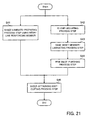
- FIG. 21 is a flowchart illustrating the outline of a process for manufacturing RFID units according to the fourth embodiment.
- Step S41 In this process step, the same method as employed in the step S21 in FIG. 9 is used to prepare a sheet laminate by sandwiching a mesh-like reinforcing member between protective sheet members. The prepared sheet laminate is taken up by a roll.
- Step S42 Separately from the step S41 for the above-described sheet laminate, a process step for mounting IC chips on a sheet member is performed. First, by the same method as employed in the steps S22 and S23 in FIG. 9 , an antenna substrate formed with antenna patterns is prepared, and the IC chips are mounted on the antenna substrate.
- Step S43 A base sheet member is disposed on the antenna substrate having the IC chips mounted thereon.
- the base sheet member having an adhesive agent attached thereto is fixedly attached to a lower surface of the antenna substrate, i.e. a surface of the antenna substrate where no IC chips are mounted.
- Step S45 The same method as employed in the step S25 in FIG. 9 is employed to sandwich the base sheet member having the RFID inlets mounted thereon between the sheet laminates prepared in the step S41 on the opposite sides thereof, whereby the adjacent sheet members are fixedly attached to each other. Further, the members fixedly attached are cut out in units of regions each including a RFID tag, whereby RFID units are completed.
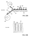
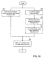
- Step S51 In this process step, by the same method as employed in the step S31 in FIG. 15 , a hard reinforcing member is mounted on a protective sheet member, and positioning sprocket holes are formed.
- the protective sheet member having the reinforcing member mounted thereon is taken up by a roll.
- all of the rubber sheets 301a, 301b and 412a and the spacer sheet 330 are laminated one upon another at a time.
- a procedure may be employed in which adjacent ones of the sheet members are laminated in advance, and e.g. after taking up the sheet laminates by respective rolls, all the sheet members are finally laminated one upon another.
- the sheet members may be fixedly attached each time the adjacent ones of the sheet members are laminated one upon another or which a final lamination process step is executed.
Landscapes
- Engineering & Computer Science (AREA)
- Computer Hardware Design (AREA)
- Microelectronics & Electronic Packaging (AREA)
- Physics & Mathematics (AREA)
- General Physics & Mathematics (AREA)
- Theoretical Computer Science (AREA)
- Credit Cards Or The Like (AREA)
Applications Claiming Priority (1)
| Application Number | Priority Date | Filing Date | Title |
|---|---|---|---|
| JP2008255891A JP5199010B2 (ja) | 2008-10-01 | 2008-10-01 | Rfidタグの製造方法およびrfidタグ |
Publications (3)
| Publication Number | Publication Date |
|---|---|
| EP2172878A2 true EP2172878A2 (de) | 2010-04-07 |
| EP2172878A3 EP2172878A3 (de) | 2015-07-01 |
| EP2172878B1 EP2172878B1 (de) | 2017-12-13 |
Family
ID=41467338
Family Applications (1)
| Application Number | Title | Priority Date | Filing Date |
|---|---|---|---|
| EP09171507.8A Not-in-force EP2172878B1 (de) | 2008-10-01 | 2009-09-28 | Verfahren zur Herstellung von RFID-Etiketten und RFID-Etiketten |
Country Status (5)
| Country | Link |
|---|---|
| US (1) | US8430324B2 (de) |
| EP (1) | EP2172878B1 (de) |
| JP (1) | JP5199010B2 (de) |
| KR (1) | KR101043701B1 (de) |
| CN (1) | CN101714218B (de) |
Cited By (32)
| Publication number | Priority date | Publication date | Assignee | Title |
|---|---|---|---|---|
| CN102737271A (zh) * | 2011-03-30 | 2012-10-17 | 富士通株式会社 | Rfid标签 |
| FR2997783A1 (fr) * | 2012-11-06 | 2014-05-09 | Oberthur Technologies | Procede et dispositif de fabrication d'une antenne |
| EP2657889A3 (de) * | 2012-04-23 | 2015-07-15 | Assa Abloy Ab | Flexibles Etikett |
| EP3026599A1 (de) * | 2014-11-28 | 2016-06-01 | Gemalto Sa | Verfahren zur Herstellung von elektronischen Vorrichtungen mit Personalisierungsinformation |
| EP3109799A3 (de) * | 2015-04-15 | 2017-02-15 | Maintag | Herstellungsverfahren eines mehrschichtenetiketts vom typ rfid, rfid-mehrschichtenetikett und seine anwendung |
| US10586144B2 (en) | 2014-09-29 | 2020-03-10 | Avery Dennison Corporation | Tire tracking RFID label |
| WO2020225668A1 (en) * | 2019-05-03 | 2020-11-12 | Bridgestone Europe Nv/Sa | Processing method for inserting electronic devices that are suitable for communicating in radio frequency into respective rubber sleeves |
| WO2020260115A1 (de) * | 2019-06-26 | 2020-12-30 | Continental Reifen Deutschland Gmbh | Verfahren und vorrichtung zur herstellung eines gummibauteiles |
| US10986816B2 (en) | 2014-03-26 | 2021-04-27 | Scr Engineers Ltd. | Livestock location system |
| US10986817B2 (en) | 2014-09-05 | 2021-04-27 | Intervet Inc. | Method and system for tracking health in animal populations |
| US11071279B2 (en) | 2014-09-05 | 2021-07-27 | Intervet Inc. | Method and system for tracking health in animal populations |
| IT202000030686A1 (it) * | 2020-12-14 | 2022-06-14 | Pirelli Tyre Spa | Gommatura di componenti elettronici |
| USD990063S1 (en) | 2020-06-18 | 2023-06-20 | S.C.R. (Engineers) Limited | Animal ear tag |
| USD990062S1 (en) | 2020-06-18 | 2023-06-20 | S.C.R. (Engineers) Limited | Animal ear tag |
| RU2808041C2 (ru) * | 2019-05-03 | 2023-11-22 | Бриджстоун Юроп Нв/Са | Способ для вставления электронных устройств, приспособленных для связи на радиочастоте, в соответствующие резиновые кожухи |
| US11832587B2 (en) | 2020-06-18 | 2023-12-05 | S.C.R. (Engineers) Limited | Animal tag |
| US11832584B2 (en) | 2018-04-22 | 2023-12-05 | Vence, Corp. | Livestock management system and method |
| US11864529B2 (en) | 2018-10-10 | 2024-01-09 | S.C.R. (Engineers) Limited | Livestock dry off method and device |
| US11960957B2 (en) | 2020-11-25 | 2024-04-16 | Identigen Limited | System and method for tracing members of an animal population |
| US20240169177A1 (en) * | 2021-06-30 | 2024-05-23 | Bridgestone Corporation | Rf tag laminate manufacturing method and rf tag laminate |
| US12099893B2 (en) | 2020-07-01 | 2024-09-24 | S.C.R. (Engineers) Limited | Device assignment system and method |
| US12144320B2 (en) | 2019-02-08 | 2024-11-19 | Allflex Australia Pty Ltd | Electronic animal identification tag reader synchronisation |
| US12193413B2 (en) | 2019-02-08 | 2025-01-14 | Allflex Australia Pty Ltd | Electronic animal tag reader |
| US12213449B2 (en) | 2021-01-24 | 2025-02-04 | S.C.R. (Engineers) Limited | Animal marking control system and method |
| US12239098B2 (en) | 2019-02-08 | 2025-03-04 | Allflex Australia Pty Ltd | Determining the location of an animal |
| USD1067554S1 (en) | 2021-04-08 | 2025-03-18 | Allflex Australia Pty Limited | Tag applicator for animals |
| USD1067544S1 (en) | 2021-04-08 | 2025-03-18 | Allflex Australia Pty Limited | Tag applicator for animals |
| US12402599B2 (en) | 2018-10-03 | 2025-09-02 | Allflex Europe Sas | Gripper for manipulating a device for identifying an animal and/or removing tissue from an animal comprising holding means with remote actuation |
| US12402596B2 (en) | 2022-05-03 | 2025-09-02 | S.C.R. (Engineers) Limited | Milk channel and feed inlet coupled thereto, and system and method for conserving wash fluid in a washing process for cleaning a milkmeter system |
| US12409474B2 (en) | 2019-08-28 | 2025-09-09 | S.C.R. (Engineers) Limited | Devices for analysis of a fluid |
| US12555124B2 (en) | 2021-06-03 | 2026-02-17 | S.C.R. (Engineers) Limited | System and method for estimating greenhouse gas emissions in an environment housing an animal population |
| US12580086B2 (en) | 2021-02-09 | 2026-03-17 | S.C.R. (Engineers) Limited | System and method for evaluating the level of harassment of insects on a plurality of animals |
Families Citing this family (30)
| Publication number | Priority date | Publication date | Assignee | Title |
|---|---|---|---|---|
| WO2012062965A1 (en) * | 2010-11-08 | 2012-05-18 | Upm Rfid Oy | A method for producing an rfid transponder |
| DE102011104170A1 (de) * | 2011-06-14 | 2012-12-20 | Schreiner Group Gmbh & Co. Kg | Transponderetikett und Herstellungsverfahren für ein Transponderetikett |
| JP5709692B2 (ja) * | 2011-08-26 | 2015-04-30 | サトーホールディングス株式会社 | ランドリー用rfidタグ |
| US20160148086A1 (en) * | 2013-06-19 | 2016-05-26 | Ross Robert Clarke | Radio Frequency Identification Tag |
| JP6232847B2 (ja) | 2013-08-28 | 2017-11-22 | 富士通株式会社 | Rfidタグ |
| US9897292B1 (en) | 2013-10-30 | 2018-02-20 | Automated Assembly Corporation | Solid-state lighting elements on adhesive transfer tape |
| US10169698B1 (en) * | 2013-10-30 | 2019-01-01 | Automated Assembly Corporation | RF transponder on adhesive transfer tape |
| US9379289B1 (en) | 2013-10-30 | 2016-06-28 | Automated Assembly Corporation | LEDs on adhesive transfer tape |
| US10402713B1 (en) | 2013-10-30 | 2019-09-03 | Automated Assembly Corporation | RF transponder on adhesive transfer tape |
| CN204650569U (zh) * | 2014-04-22 | 2015-09-16 | 株式会社村田制作所 | 无线通信标签 |
| JP2018502193A (ja) | 2014-12-22 | 2018-01-25 | ブリヂストン アメリカズ タイヤ オペレーションズ、 エルエルシー | タイヤ内の無線デバイス用のゴム組成物 |
| CN107615098A (zh) * | 2015-04-09 | 2018-01-19 | Mdt创新私人有限公司 | 用于制造rfid标签的方法 |
| JP6574367B2 (ja) * | 2015-09-29 | 2019-09-11 | 小林クリエイト株式会社 | 帳票紙片におけるrfidラベルの貼付構造、およびrfidラベルの貼付方法 |
| EP3374452B1 (de) | 2015-11-09 | 2021-04-14 | Bridgestone Americas Tire Operations, LLC | Gummibeschichtung für ein elektronisches kommunikationsmodul, elektronisches modul damit und zugehörige verfahren |
| GB201523093D0 (en) * | 2015-12-30 | 2016-02-10 | Univ Nottingham Trent | Electronic strip yarn |
| CA3013196A1 (en) * | 2016-02-04 | 2017-08-10 | Parker-Hannifin Corporation | Ruggedized radio frequency identification tags |
| WO2017183599A1 (ja) * | 2016-04-19 | 2017-10-26 | 株式会社村田製作所 | フレキシブル基板 |
| US10032104B2 (en) | 2016-06-02 | 2018-07-24 | Fujitsu Limited | RFID tag |
| CN107973163B (zh) * | 2017-11-17 | 2024-04-02 | 青岛海威物联科技有限公司 | 轮胎用rfid电子标签的层合设备 |
| CN109034339A (zh) * | 2018-06-27 | 2018-12-18 | 永道无线射频标签(扬州)有限公司 | 一种免折半贴标签及其加工方法和应用 |
| US10398873B1 (en) | 2018-07-20 | 2019-09-03 | Automated Assembly Corporation | Rolled substrate cable |
| JP7301468B2 (ja) * | 2019-04-17 | 2023-07-03 | 株式会社ディスコ | 被加工物の加工方法、熱圧着方法 |
| DE102019207402A1 (de) * | 2019-05-21 | 2020-11-26 | Continental Reifen Deutschland Gmbh | Verfahren und Vorrichtung zur Herstellung eines Gummibauteiles |
| EP4104101B1 (de) * | 2020-02-12 | 2024-11-13 | Avery Dennison Retail Information Services LLC | Übertragung von rfid-inlays von einem ersten substrat zu einem zweiten substrat |
| US12099889B2 (en) | 2021-01-20 | 2024-09-24 | Westrock Shared Services, Llc | Multi stream RFID tag applicator |
| CN114559705A (zh) * | 2022-01-13 | 2022-05-31 | 深圳市哈德胜精密科技股份有限公司 | 一种rfid标签芯片单张对裱工艺 |
| IT202200003290A1 (it) * | 2022-02-22 | 2023-08-22 | Pearfid Soc A Responsabilita Limitata Semplificata | Metodo di realizzazione di dispositivi a radiofrequenza |
| TWM648265U (zh) * | 2023-07-07 | 2023-11-11 | 振鋒企業股份有限公司 | 具有無線射頻辨識裝置之束帶 |
| CN119761401A (zh) * | 2024-04-03 | 2025-04-04 | 上海数佑信息科技有限公司 | Rfid标签元件和具有rfid标签元件的工具 |
| FR3163477A1 (fr) * | 2024-06-17 | 2025-12-19 | Paragon Id | Procédé de fabrication d’étiquettes RFID |
Citations (3)
| Publication number | Priority date | Publication date | Assignee | Title |
|---|---|---|---|---|
| JPH10181261A (ja) | 1996-12-20 | 1998-07-07 | Dainippon Printing Co Ltd | 非接触icカード |
| JP2000200333A (ja) | 1999-01-08 | 2000-07-18 | Hitachi Ltd | Icカ―ドおよびその製造方法 |
| JP2003141486A (ja) | 2001-11-08 | 2003-05-16 | Oji Paper Co Ltd | 非接触icカードとその製造方法 |
Family Cites Families (24)
| Publication number | Priority date | Publication date | Assignee | Title |
|---|---|---|---|---|
| KR100308801B1 (ko) * | 1993-03-18 | 2001-12-15 | 쿠델스키 안드레, 드로즈 프랑소와 | 전자요소를포함하는카드의제조방법및이에따라제조된카드 |
| SE9701612D0 (sv) * | 1997-04-29 | 1997-04-29 | Johan Asplund | Smartcard and method for its manufacture |
| US6019865A (en) * | 1998-01-21 | 2000-02-01 | Moore U.S.A. Inc. | Method of forming labels containing transponders |
| US6250554B1 (en) * | 1998-06-23 | 2001-06-26 | Agfa-Gevaert | Chip card comprising an imaged-receiving layer |
| JP4508301B2 (ja) * | 1998-09-16 | 2010-07-21 | 大日本印刷株式会社 | 非接触icカード |
| JP3361489B2 (ja) * | 1998-10-02 | 2003-01-07 | 新光電気工業株式会社 | Icカードの製造方法 |
| US6509630B1 (en) * | 1999-03-11 | 2003-01-21 | Seiko Epson Corporation | Flexible interconnecting substrate, film, carrier, tape-shaped semiconductor device, semiconductor device and method of manufacturing the same, circuit board, and electronic equipment |
| US7845569B1 (en) * | 1999-06-16 | 2010-12-07 | Vanguard Identification Systems, Inc. | Permanent RFID luggage tag with security features |
| US6140146A (en) * | 1999-08-03 | 2000-10-31 | Intermec Ip Corp. | Automated RFID transponder manufacturing on flexible tape substrates |
| JP2001319211A (ja) * | 2000-05-11 | 2001-11-16 | Kyodo Printing Co Ltd | Icカードおよびその製造方法 |
| JP2002187223A (ja) * | 2000-12-22 | 2002-07-02 | Sato Corp | Icインレット仮着帯の製造方法およびic内蔵表示札の製造方法 |
| JP4736191B2 (ja) * | 2001-01-22 | 2011-07-27 | 大日本印刷株式会社 | Icカードとその製造方法 |
| JP2002222403A (ja) * | 2001-01-25 | 2002-08-09 | Konica Corp | Ic搭載カード基材、ic搭載個人認証用カード及びその製造方法 |
| JP2002298107A (ja) * | 2001-03-30 | 2002-10-11 | Toppan Forms Co Ltd | 非接触型icメディアおよびその製造方法 |
| JP2003256794A (ja) * | 2002-02-28 | 2003-09-12 | Konica Corp | Icカードの製造方法及びicカード |
| US7172670B2 (en) * | 2002-12-06 | 2007-02-06 | Quality Assured Enterprises, Inc. | Single-pass, in-line process for manufacturing multi-part articles |
| US7120987B2 (en) * | 2003-08-05 | 2006-10-17 | Avery Dennison Corporation | Method of making RFID device |
| JP4479209B2 (ja) * | 2003-10-10 | 2010-06-09 | パナソニック株式会社 | 電子回路装置およびその製造方法並びに電子回路装置の製造装置 |
| US7353598B2 (en) * | 2004-11-08 | 2008-04-08 | Alien Technology Corporation | Assembly comprising functional devices and method of making same |
| JP2006134249A (ja) * | 2004-11-09 | 2006-05-25 | Fujitsu Ltd | Rfidタグ |
| CN100538731C (zh) * | 2006-02-10 | 2009-09-09 | 富士通株式会社 | Rfid标签制造方法和rfid标签 |
| JP4855849B2 (ja) * | 2006-06-30 | 2012-01-18 | 富士通株式会社 | Rfidタグの製造方法、およびrfidタグ |
| JP4382802B2 (ja) * | 2006-08-10 | 2009-12-16 | 富士通株式会社 | Rfidタグ |
| JP4946505B2 (ja) | 2007-02-27 | 2012-06-06 | 大日本印刷株式会社 | 補強板搭載rf−idタグカード |
-
2008
- 2008-10-01 JP JP2008255891A patent/JP5199010B2/ja not_active Expired - Fee Related
-
2009
- 2009-09-23 KR KR1020090090134A patent/KR101043701B1/ko not_active Expired - Fee Related
- 2009-09-24 CN CN2009101719938A patent/CN101714218B/zh not_active Expired - Fee Related
- 2009-09-28 US US12/567,989 patent/US8430324B2/en not_active Expired - Fee Related
- 2009-09-28 EP EP09171507.8A patent/EP2172878B1/de not_active Not-in-force
Patent Citations (3)
| Publication number | Priority date | Publication date | Assignee | Title |
|---|---|---|---|---|
| JPH10181261A (ja) | 1996-12-20 | 1998-07-07 | Dainippon Printing Co Ltd | 非接触icカード |
| JP2000200333A (ja) | 1999-01-08 | 2000-07-18 | Hitachi Ltd | Icカ―ドおよびその製造方法 |
| JP2003141486A (ja) | 2001-11-08 | 2003-05-16 | Oji Paper Co Ltd | 非接触icカードとその製造方法 |
Cited By (48)
| Publication number | Priority date | Publication date | Assignee | Title |
|---|---|---|---|---|
| CN102737271A (zh) * | 2011-03-30 | 2012-10-17 | 富士通株式会社 | Rfid标签 |
| EP2506192A3 (de) * | 2011-03-30 | 2014-04-02 | Fujitsu Limited | RFID-Etikett |
| US8763911B2 (en) | 2011-03-30 | 2014-07-01 | Fujitsu Limited | RFID tag |
| CN102737271B (zh) * | 2011-03-30 | 2015-04-29 | 富士通株式会社 | Rfid标签 |
| EP2657889A3 (de) * | 2012-04-23 | 2015-07-15 | Assa Abloy Ab | Flexibles Etikett |
| FR2997783A1 (fr) * | 2012-11-06 | 2014-05-09 | Oberthur Technologies | Procede et dispositif de fabrication d'une antenne |
| US10986816B2 (en) | 2014-03-26 | 2021-04-27 | Scr Engineers Ltd. | Livestock location system |
| US12213455B2 (en) | 2014-03-26 | 2025-02-04 | S.C.R. (Engineers) Limited | Livestock location system |
| US11963515B2 (en) | 2014-03-26 | 2024-04-23 | S.C.R. (Engineers) Limited | Livestock location system |
| US10986817B2 (en) | 2014-09-05 | 2021-04-27 | Intervet Inc. | Method and system for tracking health in animal populations |
| US11071279B2 (en) | 2014-09-05 | 2021-07-27 | Intervet Inc. | Method and system for tracking health in animal populations |
| US10586144B2 (en) | 2014-09-29 | 2020-03-10 | Avery Dennison Corporation | Tire tracking RFID label |
| US11494604B2 (en) | 2014-09-29 | 2022-11-08 | Avey Dennison Corporation | Tire tracking RFID label |
| US10997487B2 (en) | 2014-09-29 | 2021-05-04 | Avery Dennison Corporation | Tire tracking RFID label |
| US11763127B2 (en) | 2014-09-29 | 2023-09-19 | Avery Dennison Corporation | Tire tracking RFID label |
| WO2016083403A1 (fr) * | 2014-11-28 | 2016-06-02 | Gemalto Sa | Procede de fabrication de dispositifs electroniques avec information de personnalisation |
| EP3026599A1 (de) * | 2014-11-28 | 2016-06-01 | Gemalto Sa | Verfahren zur Herstellung von elektronischen Vorrichtungen mit Personalisierungsinformation |
| EP3109799A3 (de) * | 2015-04-15 | 2017-02-15 | Maintag | Herstellungsverfahren eines mehrschichtenetiketts vom typ rfid, rfid-mehrschichtenetikett und seine anwendung |
| US11832584B2 (en) | 2018-04-22 | 2023-12-05 | Vence, Corp. | Livestock management system and method |
| US12593824B2 (en) | 2018-04-22 | 2026-04-07 | Vence, Corp. | Livestock management system and method |
| US12402599B2 (en) | 2018-10-03 | 2025-09-02 | Allflex Europe Sas | Gripper for manipulating a device for identifying an animal and/or removing tissue from an animal comprising holding means with remote actuation |
| US12133507B2 (en) | 2018-10-10 | 2024-11-05 | S.C.R. (Engineers) Limited | Livestock dry off method and device |
| US11864529B2 (en) | 2018-10-10 | 2024-01-09 | S.C.R. (Engineers) Limited | Livestock dry off method and device |
| US12239098B2 (en) | 2019-02-08 | 2025-03-04 | Allflex Australia Pty Ltd | Determining the location of an animal |
| US12193413B2 (en) | 2019-02-08 | 2025-01-14 | Allflex Australia Pty Ltd | Electronic animal tag reader |
| US12144320B2 (en) | 2019-02-08 | 2024-11-19 | Allflex Australia Pty Ltd | Electronic animal identification tag reader synchronisation |
| RU2808041C2 (ru) * | 2019-05-03 | 2023-11-22 | Бриджстоун Юроп Нв/Са | Способ для вставления электронных устройств, приспособленных для связи на радиочастоте, в соответствующие резиновые кожухи |
| WO2020225668A1 (en) * | 2019-05-03 | 2020-11-12 | Bridgestone Europe Nv/Sa | Processing method for inserting electronic devices that are suitable for communicating in radio frequency into respective rubber sleeves |
| US12017426B2 (en) | 2019-05-03 | 2024-06-25 | Bridgestone Europe NV/SA [BE/BE] | Processing method for inserting electronic devices that are suitable for communicating in radio frequency into respective rubber sleeves |
| WO2020260115A1 (de) * | 2019-06-26 | 2020-12-30 | Continental Reifen Deutschland Gmbh | Verfahren und vorrichtung zur herstellung eines gummibauteiles |
| US12409474B2 (en) | 2019-08-28 | 2025-09-09 | S.C.R. (Engineers) Limited | Devices for analysis of a fluid |
| US12342790B2 (en) | 2020-06-18 | 2025-07-01 | S.C.R. (Engineers) Limited | Animal tag |
| USD990062S1 (en) | 2020-06-18 | 2023-06-20 | S.C.R. (Engineers) Limited | Animal ear tag |
| US11832587B2 (en) | 2020-06-18 | 2023-12-05 | S.C.R. (Engineers) Limited | Animal tag |
| USD990063S1 (en) | 2020-06-18 | 2023-06-20 | S.C.R. (Engineers) Limited | Animal ear tag |
| US12099893B2 (en) | 2020-07-01 | 2024-09-24 | S.C.R. (Engineers) Limited | Device assignment system and method |
| US12321808B2 (en) | 2020-11-25 | 2025-06-03 | Identigen Limited | System and method for tracing members of an animal population |
| US11960957B2 (en) | 2020-11-25 | 2024-04-16 | Identigen Limited | System and method for tracing members of an animal population |
| IT202000030686A1 (it) * | 2020-12-14 | 2022-06-14 | Pirelli Tyre Spa | Gommatura di componenti elettronici |
| WO2022130144A1 (en) * | 2020-12-14 | 2022-06-23 | Pirelli Tyre S.P.A. | Rubber-coating of electronic components |
| US12213449B2 (en) | 2021-01-24 | 2025-02-04 | S.C.R. (Engineers) Limited | Animal marking control system and method |
| US12580086B2 (en) | 2021-02-09 | 2026-03-17 | S.C.R. (Engineers) Limited | System and method for evaluating the level of harassment of insects on a plurality of animals |
| USD1067544S1 (en) | 2021-04-08 | 2025-03-18 | Allflex Australia Pty Limited | Tag applicator for animals |
| USD1067554S1 (en) | 2021-04-08 | 2025-03-18 | Allflex Australia Pty Limited | Tag applicator for animals |
| US12555124B2 (en) | 2021-06-03 | 2026-02-17 | S.C.R. (Engineers) Limited | System and method for estimating greenhouse gas emissions in an environment housing an animal population |
| US12434465B2 (en) * | 2021-06-30 | 2025-10-07 | Bridgestone Corporation | RF tag laminate manufacturing method and RF tag laminate |
| US20240169177A1 (en) * | 2021-06-30 | 2024-05-23 | Bridgestone Corporation | Rf tag laminate manufacturing method and rf tag laminate |
| US12402596B2 (en) | 2022-05-03 | 2025-09-02 | S.C.R. (Engineers) Limited | Milk channel and feed inlet coupled thereto, and system and method for conserving wash fluid in a washing process for cleaning a milkmeter system |
Also Published As
| Publication number | Publication date |
|---|---|
| KR101043701B1 (ko) | 2011-06-24 |
| CN101714218A (zh) | 2010-05-26 |
| US8430324B2 (en) | 2013-04-30 |
| JP2010086361A (ja) | 2010-04-15 |
| EP2172878A3 (de) | 2015-07-01 |
| EP2172878B1 (de) | 2017-12-13 |
| US20100078487A1 (en) | 2010-04-01 |
| CN101714218B (zh) | 2013-03-20 |
| JP5199010B2 (ja) | 2013-05-15 |
| KR20100037546A (ko) | 2010-04-09 |
Similar Documents
| Publication | Publication Date | Title |
|---|---|---|
| EP2172878B1 (de) | Verfahren zur Herstellung von RFID-Etiketten und RFID-Etiketten | |
| JP3803097B2 (ja) | 無線通信媒体の製造方法 | |
| KR100825524B1 (ko) | Rfid 태그의 제조 방법 및 rfid 태그 | |
| JP6512385B2 (ja) | Rfidタグ | |
| WO2006005985A1 (en) | Contactless identification device | |
| US20140361090A1 (en) | Rfid tag and rfid tag manufacturing method | |
| CN113168551A (zh) | Rfid标签和rfid标牌 | |
| EP1962233B1 (de) | Funkfrequenz-Kennzeichnung und Verfahren zur Herstellung der Funkfrequenz-Kennzeichnung | |
| JP7136383B2 (ja) | Rfidタグ製造システム | |
| JP2009116649A (ja) | Rfidタグ | |
| KR100760504B1 (ko) | Rfid 태그 | |
| JP4386023B2 (ja) | Ic実装モジュールの製造方法および製造装置 | |
| JP2013242698A (ja) | 無線icモジュール付き基材シートの製造方法 | |
| US20140224882A1 (en) | Flexible Smart Card Transponder | |
| JP5771946B2 (ja) | 非接触及び接触共用icカード | |
| JP2003132331A (ja) | 非接触データキャリア用基材と非接触データキャリア | |
| JP2005115916A (ja) | 無線通信媒体およびその製造方法 | |
| JP2007157140A (ja) | 無線周波装置 | |
| EP1804203A2 (de) | RFID-Etikett | |
| JP2017227959A (ja) | 非接触型情報媒体及び非接触型情報媒体の製造方法 | |
| JP4930758B2 (ja) | 非接触型データキャリア装置とその作製方法 | |
| WO2008001729A1 (en) | Ic tag and ic tag sheet | |
| JP5928568B2 (ja) | 非接触及び接触共用icカード | |
| JP2010160706A (ja) | 非接触icタグ類 | |
| KR20090084499A (ko) | 무선 주파수 인식 태그의 제조방법 및 이에 의해 제조된무선 주파수 인식태그 |
Legal Events
| Date | Code | Title | Description |
|---|---|---|---|
| PUAI | Public reference made under article 153(3) epc to a published international application that has entered the european phase |
Free format text: ORIGINAL CODE: 0009012 |
|
| AK | Designated contracting states |
Kind code of ref document: A2 Designated state(s): AT BE BG CH CY CZ DE DK EE ES FI FR GB GR HR HU IE IS IT LI LT LU LV MC MK MT NL NO PL PT RO SE SI SK SM TR |
|
| AX | Request for extension of the european patent |
Extension state: AL BA RS |
|
| PUAL | Search report despatched |
Free format text: ORIGINAL CODE: 0009013 |
|
| AK | Designated contracting states |
Kind code of ref document: A3 Designated state(s): AT BE BG CH CY CZ DE DK EE ES FI FR GB GR HR HU IE IS IT LI LT LU LV MC MK MT NL NO PL PT RO SE SI SK SM TR |
|
| AX | Request for extension of the european patent |
Extension state: AL BA RS |
|
| RIC1 | Information provided on ipc code assigned before grant |
Ipc: G06K 19/077 20060101AFI20150528BHEP |
|
| 17P | Request for examination filed |
Effective date: 20151020 |
|
| RBV | Designated contracting states (corrected) |
Designated state(s): AT BE BG CH CY CZ DE DK EE ES FI FR GB GR HR HU IE IS IT LI LT LU LV MC MK MT NL NO PL PT RO SE SI SK SM TR |
|
| GRAP | Despatch of communication of intention to grant a patent |
Free format text: ORIGINAL CODE: EPIDOSNIGR1 |
|
| INTG | Intention to grant announced |
Effective date: 20170629 |
|
| GRAS | Grant fee paid |
Free format text: ORIGINAL CODE: EPIDOSNIGR3 |
|
| GRAA | (expected) grant |
Free format text: ORIGINAL CODE: 0009210 |
|
| AK | Designated contracting states |
Kind code of ref document: B1 Designated state(s): AT BE BG CH CY CZ DE DK EE ES FI FR GB GR HR HU IE IS IT LI LT LU LV MC MK MT NL NO PL PT RO SE SI SK SM TR |
|
| REG | Reference to a national code |
Ref country code: GB Ref legal event code: FG4D |
|
| REG | Reference to a national code |
Ref country code: AT Ref legal event code: REF Ref document number: 955058 Country of ref document: AT Kind code of ref document: T Effective date: 20171215 Ref country code: CH Ref legal event code: EP |
|
| REG | Reference to a national code |
Ref country code: IE Ref legal event code: FG4D |
|
| REG | Reference to a national code |
Ref country code: DE Ref legal event code: R096 Ref document number: 602009049843 Country of ref document: DE |
|
| REG | Reference to a national code |
Ref country code: NL Ref legal event code: MP Effective date: 20171213 |
|
| REG | Reference to a national code |
Ref country code: LT Ref legal event code: MG4D |
|
| PG25 | Lapsed in a contracting state [announced via postgrant information from national office to epo] |
Ref country code: FI Free format text: LAPSE BECAUSE OF FAILURE TO SUBMIT A TRANSLATION OF THE DESCRIPTION OR TO PAY THE FEE WITHIN THE PRESCRIBED TIME-LIMIT Effective date: 20171213 Ref country code: LT Free format text: LAPSE BECAUSE OF FAILURE TO SUBMIT A TRANSLATION OF THE DESCRIPTION OR TO PAY THE FEE WITHIN THE PRESCRIBED TIME-LIMIT Effective date: 20171213 Ref country code: NO Free format text: LAPSE BECAUSE OF FAILURE TO SUBMIT A TRANSLATION OF THE DESCRIPTION OR TO PAY THE FEE WITHIN THE PRESCRIBED TIME-LIMIT Effective date: 20180313 Ref country code: SE Free format text: LAPSE BECAUSE OF FAILURE TO SUBMIT A TRANSLATION OF THE DESCRIPTION OR TO PAY THE FEE WITHIN THE PRESCRIBED TIME-LIMIT Effective date: 20171213 |
|
| REG | Reference to a national code |
Ref country code: AT Ref legal event code: MK05 Ref document number: 955058 Country of ref document: AT Kind code of ref document: T Effective date: 20171213 |
|
| PG25 | Lapsed in a contracting state [announced via postgrant information from national office to epo] |
Ref country code: HR Free format text: LAPSE BECAUSE OF FAILURE TO SUBMIT A TRANSLATION OF THE DESCRIPTION OR TO PAY THE FEE WITHIN THE PRESCRIBED TIME-LIMIT Effective date: 20171213 Ref country code: LV Free format text: LAPSE BECAUSE OF FAILURE TO SUBMIT A TRANSLATION OF THE DESCRIPTION OR TO PAY THE FEE WITHIN THE PRESCRIBED TIME-LIMIT Effective date: 20171213 Ref country code: BG Free format text: LAPSE BECAUSE OF FAILURE TO SUBMIT A TRANSLATION OF THE DESCRIPTION OR TO PAY THE FEE WITHIN THE PRESCRIBED TIME-LIMIT Effective date: 20180313 Ref country code: GR Free format text: LAPSE BECAUSE OF FAILURE TO SUBMIT A TRANSLATION OF THE DESCRIPTION OR TO PAY THE FEE WITHIN THE PRESCRIBED TIME-LIMIT Effective date: 20180314 |
|
| PG25 | Lapsed in a contracting state [announced via postgrant information from national office to epo] |
Ref country code: NL Free format text: LAPSE BECAUSE OF FAILURE TO SUBMIT A TRANSLATION OF THE DESCRIPTION OR TO PAY THE FEE WITHIN THE PRESCRIBED TIME-LIMIT Effective date: 20171213 |
|
| PG25 | Lapsed in a contracting state [announced via postgrant information from national office to epo] |
Ref country code: SK Free format text: LAPSE BECAUSE OF FAILURE TO SUBMIT A TRANSLATION OF THE DESCRIPTION OR TO PAY THE FEE WITHIN THE PRESCRIBED TIME-LIMIT Effective date: 20171213 Ref country code: CZ Free format text: LAPSE BECAUSE OF FAILURE TO SUBMIT A TRANSLATION OF THE DESCRIPTION OR TO PAY THE FEE WITHIN THE PRESCRIBED TIME-LIMIT Effective date: 20171213 Ref country code: ES Free format text: LAPSE BECAUSE OF FAILURE TO SUBMIT A TRANSLATION OF THE DESCRIPTION OR TO PAY THE FEE WITHIN THE PRESCRIBED TIME-LIMIT Effective date: 20171213 Ref country code: CY Free format text: LAPSE BECAUSE OF FAILURE TO SUBMIT A TRANSLATION OF THE DESCRIPTION OR TO PAY THE FEE WITHIN THE PRESCRIBED TIME-LIMIT Effective date: 20171213 Ref country code: EE Free format text: LAPSE BECAUSE OF FAILURE TO SUBMIT A TRANSLATION OF THE DESCRIPTION OR TO PAY THE FEE WITHIN THE PRESCRIBED TIME-LIMIT Effective date: 20171213 |
|
| PG25 | Lapsed in a contracting state [announced via postgrant information from national office to epo] |
Ref country code: IS Free format text: LAPSE BECAUSE OF FAILURE TO SUBMIT A TRANSLATION OF THE DESCRIPTION OR TO PAY THE FEE WITHIN THE PRESCRIBED TIME-LIMIT Effective date: 20180413 Ref country code: SM Free format text: LAPSE BECAUSE OF FAILURE TO SUBMIT A TRANSLATION OF THE DESCRIPTION OR TO PAY THE FEE WITHIN THE PRESCRIBED TIME-LIMIT Effective date: 20171213 Ref country code: IT Free format text: LAPSE BECAUSE OF FAILURE TO SUBMIT A TRANSLATION OF THE DESCRIPTION OR TO PAY THE FEE WITHIN THE PRESCRIBED TIME-LIMIT Effective date: 20171213 Ref country code: PL Free format text: LAPSE BECAUSE OF FAILURE TO SUBMIT A TRANSLATION OF THE DESCRIPTION OR TO PAY THE FEE WITHIN THE PRESCRIBED TIME-LIMIT Effective date: 20171213 Ref country code: RO Free format text: LAPSE BECAUSE OF FAILURE TO SUBMIT A TRANSLATION OF THE DESCRIPTION OR TO PAY THE FEE WITHIN THE PRESCRIBED TIME-LIMIT Effective date: 20171213 Ref country code: AT Free format text: LAPSE BECAUSE OF FAILURE TO SUBMIT A TRANSLATION OF THE DESCRIPTION OR TO PAY THE FEE WITHIN THE PRESCRIBED TIME-LIMIT Effective date: 20171213 |
|
| REG | Reference to a national code |
Ref country code: DE Ref legal event code: R097 Ref document number: 602009049843 Country of ref document: DE |
|
| PLBE | No opposition filed within time limit |
Free format text: ORIGINAL CODE: 0009261 |
|
| STAA | Information on the status of an ep patent application or granted ep patent |
Free format text: STATUS: NO OPPOSITION FILED WITHIN TIME LIMIT |
|
| 26N | No opposition filed |
Effective date: 20180914 |
|
| PG25 | Lapsed in a contracting state [announced via postgrant information from national office to epo] |
Ref country code: DK Free format text: LAPSE BECAUSE OF FAILURE TO SUBMIT A TRANSLATION OF THE DESCRIPTION OR TO PAY THE FEE WITHIN THE PRESCRIBED TIME-LIMIT Effective date: 20171213 |
|
| PG25 | Lapsed in a contracting state [announced via postgrant information from national office to epo] |
Ref country code: SI Free format text: LAPSE BECAUSE OF FAILURE TO SUBMIT A TRANSLATION OF THE DESCRIPTION OR TO PAY THE FEE WITHIN THE PRESCRIBED TIME-LIMIT Effective date: 20171213 |
|
| REG | Reference to a national code |
Ref country code: DE Ref legal event code: R119 Ref document number: 602009049843 Country of ref document: DE |
|
| PG25 | Lapsed in a contracting state [announced via postgrant information from national office to epo] |
Ref country code: MC Free format text: LAPSE BECAUSE OF FAILURE TO SUBMIT A TRANSLATION OF THE DESCRIPTION OR TO PAY THE FEE WITHIN THE PRESCRIBED TIME-LIMIT Effective date: 20171213 |
|
| REG | Reference to a national code |
Ref country code: CH Ref legal event code: PL |
|
| GBPC | Gb: european patent ceased through non-payment of renewal fee |
Effective date: 20180928 |
|
| REG | Reference to a national code |
Ref country code: BE Ref legal event code: MM Effective date: 20180930 |
|
| REG | Reference to a national code |
Ref country code: IE Ref legal event code: MM4A |
|
| PG25 | Lapsed in a contracting state [announced via postgrant information from national office to epo] |
Ref country code: LU Free format text: LAPSE BECAUSE OF NON-PAYMENT OF DUE FEES Effective date: 20180928 |
|
| PG25 | Lapsed in a contracting state [announced via postgrant information from national office to epo] |
Ref country code: IE Free format text: LAPSE BECAUSE OF NON-PAYMENT OF DUE FEES Effective date: 20180928 Ref country code: DE Free format text: LAPSE BECAUSE OF NON-PAYMENT OF DUE FEES Effective date: 20190402 |
|
| PG25 | Lapsed in a contracting state [announced via postgrant information from national office to epo] |
Ref country code: LI Free format text: LAPSE BECAUSE OF NON-PAYMENT OF DUE FEES Effective date: 20180930 Ref country code: CH Free format text: LAPSE BECAUSE OF NON-PAYMENT OF DUE FEES Effective date: 20180930 Ref country code: FR Free format text: LAPSE BECAUSE OF NON-PAYMENT OF DUE FEES Effective date: 20180930 Ref country code: BE Free format text: LAPSE BECAUSE OF NON-PAYMENT OF DUE FEES Effective date: 20180930 |
|
| PG25 | Lapsed in a contracting state [announced via postgrant information from national office to epo] |
Ref country code: GB Free format text: LAPSE BECAUSE OF NON-PAYMENT OF DUE FEES Effective date: 20180928 |
|
| PG25 | Lapsed in a contracting state [announced via postgrant information from national office to epo] |
Ref country code: MT Free format text: LAPSE BECAUSE OF NON-PAYMENT OF DUE FEES Effective date: 20180928 |
|
| PG25 | Lapsed in a contracting state [announced via postgrant information from national office to epo] |
Ref country code: TR Free format text: LAPSE BECAUSE OF FAILURE TO SUBMIT A TRANSLATION OF THE DESCRIPTION OR TO PAY THE FEE WITHIN THE PRESCRIBED TIME-LIMIT Effective date: 20171213 |
|
| PG25 | Lapsed in a contracting state [announced via postgrant information from national office to epo] |
Ref country code: PT Free format text: LAPSE BECAUSE OF FAILURE TO SUBMIT A TRANSLATION OF THE DESCRIPTION OR TO PAY THE FEE WITHIN THE PRESCRIBED TIME-LIMIT Effective date: 20171213 Ref country code: HU Free format text: LAPSE BECAUSE OF FAILURE TO SUBMIT A TRANSLATION OF THE DESCRIPTION OR TO PAY THE FEE WITHIN THE PRESCRIBED TIME-LIMIT; INVALID AB INITIO Effective date: 20090928 |
|
| PG25 | Lapsed in a contracting state [announced via postgrant information from national office to epo] |
Ref country code: MK Free format text: LAPSE BECAUSE OF NON-PAYMENT OF DUE FEES Effective date: 20171213 |