EP2169791B1 - Semiconductor light emitting devices with non-epitaxial upper cladding - Google Patents
Semiconductor light emitting devices with non-epitaxial upper cladding Download PDFInfo
- Publication number
- EP2169791B1 EP2169791B1 EP09170496.5A EP09170496A EP2169791B1 EP 2169791 B1 EP2169791 B1 EP 2169791B1 EP 09170496 A EP09170496 A EP 09170496A EP 2169791 B1 EP2169791 B1 EP 2169791B1
- Authority
- EP
- European Patent Office
- Prior art keywords
- cladding layer
- light emitting
- emitting device
- semiconductor light
- layer
- Prior art date
- Legal status (The legal status is an assumption and is not a legal conclusion. Google has not performed a legal analysis and makes no representation as to the accuracy of the status listed.)
- Not-in-force
Links
- 238000005253 cladding Methods 0.000 title claims description 90
- 239000004065 semiconductor Substances 0.000 title claims description 27
- 239000000463 material Substances 0.000 claims description 37
- 229910002601 GaN Inorganic materials 0.000 claims description 35
- BQCADISMDOOEFD-UHFFFAOYSA-N Silver Chemical compound [Ag] BQCADISMDOOEFD-UHFFFAOYSA-N 0.000 claims description 35
- 229910052751 metal Inorganic materials 0.000 claims description 28
- 239000002184 metal Substances 0.000 claims description 28
- 229910052709 silver Inorganic materials 0.000 claims description 26
- 239000004332 silver Substances 0.000 claims description 26
- 229910052738 indium Inorganic materials 0.000 claims description 6
- APFVFJFRJDLVQX-UHFFFAOYSA-N indium atom Chemical compound [In] APFVFJFRJDLVQX-UHFFFAOYSA-N 0.000 claims description 4
- JMASRVWKEDWRBT-UHFFFAOYSA-N Gallium nitride Chemical compound [Ga]#N JMASRVWKEDWRBT-UHFFFAOYSA-N 0.000 claims description 3
- AMGQUBHHOARCQH-UHFFFAOYSA-N indium;oxotin Chemical compound [In].[Sn]=O AMGQUBHHOARCQH-UHFFFAOYSA-N 0.000 claims description 3
- 239000000758 substrate Substances 0.000 claims description 3
- XLOMVQKBTHCTTD-UHFFFAOYSA-N Zinc monoxide Chemical compound [Zn]=O XLOMVQKBTHCTTD-UHFFFAOYSA-N 0.000 claims description 2
- GYHNNYVSQQEPJS-UHFFFAOYSA-N Gallium Chemical compound [Ga] GYHNNYVSQQEPJS-UHFFFAOYSA-N 0.000 claims 2
- PMHQVHHXPFUNSP-UHFFFAOYSA-M copper(1+);methylsulfanylmethane;bromide Chemical compound Br[Cu].CSC PMHQVHHXPFUNSP-UHFFFAOYSA-M 0.000 claims 2
- 229910052733 gallium Inorganic materials 0.000 claims 2
- 150000004767 nitrides Chemical class 0.000 description 20
- 230000003287 optical effect Effects 0.000 description 13
- 238000002310 reflectometry Methods 0.000 description 10
- 239000000203 mixture Substances 0.000 description 9
- 229910002704 AlGaN Inorganic materials 0.000 description 7
- PXHVJJICTQNCMI-UHFFFAOYSA-N nickel Substances [Ni] PXHVJJICTQNCMI-UHFFFAOYSA-N 0.000 description 7
- 238000010521 absorption reaction Methods 0.000 description 6
- 238000004088 simulation Methods 0.000 description 6
- 229910045601 alloy Inorganic materials 0.000 description 5
- 239000000956 alloy Substances 0.000 description 5
- 230000008901 benefit Effects 0.000 description 5
- 239000006185 dispersion Substances 0.000 description 5
- 230000000737 periodic effect Effects 0.000 description 4
- 230000008033 biological extinction Effects 0.000 description 3
- 239000004020 conductor Substances 0.000 description 3
- 238000005336 cracking Methods 0.000 description 3
- 238000005530 etching Methods 0.000 description 3
- 150000002739 metals Chemical class 0.000 description 3
- QGZKDVFQNNGYKY-UHFFFAOYSA-N Ammonia Chemical compound N QGZKDVFQNNGYKY-UHFFFAOYSA-N 0.000 description 2
- 230000004888 barrier function Effects 0.000 description 2
- 230000015556 catabolic process Effects 0.000 description 2
- 239000002131 composite material Substances 0.000 description 2
- 150000001875 compounds Chemical class 0.000 description 2
- 238000006731 degradation reaction Methods 0.000 description 2
- 239000010931 gold Substances 0.000 description 2
- 238000011835 investigation Methods 0.000 description 2
- 238000000034 method Methods 0.000 description 2
- 229910052759 nickel Inorganic materials 0.000 description 2
- 238000001429 visible spectrum Methods 0.000 description 2
- 229910001218 Gallium arsenide Inorganic materials 0.000 description 1
- 229910004205 SiNX Inorganic materials 0.000 description 1
- BLRPTPMANUNPDV-UHFFFAOYSA-N Silane Chemical compound [SiH4] BLRPTPMANUNPDV-UHFFFAOYSA-N 0.000 description 1
- 230000004913 activation Effects 0.000 description 1
- 229910021529 ammonia Inorganic materials 0.000 description 1
- 230000015572 biosynthetic process Effects 0.000 description 1
- 230000000903 blocking effect Effects 0.000 description 1
- 239000013590 bulk material Substances 0.000 description 1
- 239000012159 carrier gas Substances 0.000 description 1
- 238000005229 chemical vapour deposition Methods 0.000 description 1
- 238000004891 communication Methods 0.000 description 1
- 230000008878 coupling Effects 0.000 description 1
- 238000010168 coupling process Methods 0.000 description 1
- 238000005859 coupling reaction Methods 0.000 description 1
- 230000007547 defect Effects 0.000 description 1
- 230000001419 dependent effect Effects 0.000 description 1
- 238000000151 deposition Methods 0.000 description 1
- 230000008021 deposition Effects 0.000 description 1
- 238000005137 deposition process Methods 0.000 description 1
- 230000000994 depressogenic effect Effects 0.000 description 1
- 238000000295 emission spectrum Methods 0.000 description 1
- 238000001704 evaporation Methods 0.000 description 1
- PCHJSUWPFVWCPO-UHFFFAOYSA-N gold Chemical compound [Au] PCHJSUWPFVWCPO-UHFFFAOYSA-N 0.000 description 1
- 229910052737 gold Inorganic materials 0.000 description 1
- 230000006872 improvement Effects 0.000 description 1
- 238000002347 injection Methods 0.000 description 1
- 239000007924 injection Substances 0.000 description 1
- 238000010884 ion-beam technique Methods 0.000 description 1
- QBJCZLXULXFYCK-UHFFFAOYSA-N magnesium;cyclopenta-1,3-diene Chemical compound [Mg+2].C1C=CC=[C-]1.C1C=CC=[C-]1 QBJCZLXULXFYCK-UHFFFAOYSA-N 0.000 description 1
- 238000004519 manufacturing process Methods 0.000 description 1
- 238000001465 metallisation Methods 0.000 description 1
- 238000005457 optimization Methods 0.000 description 1
- TWNQGVIAIRXVLR-UHFFFAOYSA-N oxo(oxoalumanyloxy)alumane Chemical compound O=[Al]O[Al]=O TWNQGVIAIRXVLR-UHFFFAOYSA-N 0.000 description 1
- 229910052763 palladium Inorganic materials 0.000 description 1
- 238000002161 passivation Methods 0.000 description 1
- 230000035515 penetration Effects 0.000 description 1
- 229910052697 platinum Inorganic materials 0.000 description 1
- 239000002244 precipitate Substances 0.000 description 1
- 239000002243 precursor Substances 0.000 description 1
- 230000008569 process Effects 0.000 description 1
- 230000001902 propagating effect Effects 0.000 description 1
- 229910052594 sapphire Inorganic materials 0.000 description 1
- 239000010980 sapphire Substances 0.000 description 1
- 229910000077 silane Inorganic materials 0.000 description 1
- -1 silver Chemical class 0.000 description 1
- 150000003378 silver Chemical class 0.000 description 1
- 239000007787 solid Substances 0.000 description 1
- 238000001228 spectrum Methods 0.000 description 1
- 230000007847 structural defect Effects 0.000 description 1
- YVTHLONGBIQYBO-UHFFFAOYSA-N zinc indium(3+) oxygen(2-) Chemical compound [O--].[Zn++].[In+3] YVTHLONGBIQYBO-UHFFFAOYSA-N 0.000 description 1
Images


Classifications
-
- H—ELECTRICITY
- H01—ELECTRIC ELEMENTS
- H01S—DEVICES USING THE PROCESS OF LIGHT AMPLIFICATION BY STIMULATED EMISSION OF RADIATION [LASER] TO AMPLIFY OR GENERATE LIGHT; DEVICES USING STIMULATED EMISSION OF ELECTROMAGNETIC RADIATION IN WAVE RANGES OTHER THAN OPTICAL
- H01S5/00—Semiconductor lasers
- H01S5/20—Structure or shape of the semiconductor body to guide the optical wave ; Confining structures perpendicular to the optical axis, e.g. index or gain guiding, stripe geometry, broad area lasers, gain tailoring, transverse or lateral reflectors, special cladding structures, MQW barrier reflection layers
- H01S5/22—Structure or shape of the semiconductor body to guide the optical wave ; Confining structures perpendicular to the optical axis, e.g. index or gain guiding, stripe geometry, broad area lasers, gain tailoring, transverse or lateral reflectors, special cladding structures, MQW barrier reflection layers having a ridge or stripe structure
-
- B—PERFORMING OPERATIONS; TRANSPORTING
- B82—NANOTECHNOLOGY
- B82Y—SPECIFIC USES OR APPLICATIONS OF NANOSTRUCTURES; MEASUREMENT OR ANALYSIS OF NANOSTRUCTURES; MANUFACTURE OR TREATMENT OF NANOSTRUCTURES
- B82Y20/00—Nanooptics, e.g. quantum optics or photonic crystals
-
- H—ELECTRICITY
- H01—ELECTRIC ELEMENTS
- H01S—DEVICES USING THE PROCESS OF LIGHT AMPLIFICATION BY STIMULATED EMISSION OF RADIATION [LASER] TO AMPLIFY OR GENERATE LIGHT; DEVICES USING STIMULATED EMISSION OF ELECTROMAGNETIC RADIATION IN WAVE RANGES OTHER THAN OPTICAL
- H01S5/00—Semiconductor lasers
- H01S5/04—Processes or apparatus for excitation, e.g. pumping, e.g. by electron beams
- H01S5/042—Electrical excitation ; Circuits therefor
- H01S5/0425—Electrodes, e.g. characterised by the structure
- H01S5/04252—Electrodes, e.g. characterised by the structure characterised by the material
- H01S5/04253—Electrodes, e.g. characterised by the structure characterised by the material having specific optical properties, e.g. transparent electrodes
-
- H—ELECTRICITY
- H01—ELECTRIC ELEMENTS
- H01S—DEVICES USING THE PROCESS OF LIGHT AMPLIFICATION BY STIMULATED EMISSION OF RADIATION [LASER] TO AMPLIFY OR GENERATE LIGHT; DEVICES USING STIMULATED EMISSION OF ELECTROMAGNETIC RADIATION IN WAVE RANGES OTHER THAN OPTICAL
- H01S5/00—Semiconductor lasers
- H01S5/30—Structure or shape of the active region; Materials used for the active region
- H01S5/34—Structure or shape of the active region; Materials used for the active region comprising quantum well or superlattice structures, e.g. single quantum well [SQW] lasers, multiple quantum well [MQW] lasers or graded index separate confinement heterostructure [GRINSCH] lasers
- H01S5/343—Structure or shape of the active region; Materials used for the active region comprising quantum well or superlattice structures, e.g. single quantum well [SQW] lasers, multiple quantum well [MQW] lasers or graded index separate confinement heterostructure [GRINSCH] lasers in AIIIBV compounds, e.g. AlGaAs-laser, InP-based laser
- H01S5/34333—Structure or shape of the active region; Materials used for the active region comprising quantum well or superlattice structures, e.g. single quantum well [SQW] lasers, multiple quantum well [MQW] lasers or graded index separate confinement heterostructure [GRINSCH] lasers in AIIIBV compounds, e.g. AlGaAs-laser, InP-based laser with a well layer based on Ga(In)N or Ga(In)P, e.g. blue laser
-
- H—ELECTRICITY
- H01—ELECTRIC ELEMENTS
- H01S—DEVICES USING THE PROCESS OF LIGHT AMPLIFICATION BY STIMULATED EMISSION OF RADIATION [LASER] TO AMPLIFY OR GENERATE LIGHT; DEVICES USING STIMULATED EMISSION OF ELECTROMAGNETIC RADIATION IN WAVE RANGES OTHER THAN OPTICAL
- H01S5/00—Semiconductor lasers
- H01S5/04—Processes or apparatus for excitation, e.g. pumping, e.g. by electron beams
- H01S5/042—Electrical excitation ; Circuits therefor
- H01S5/0425—Electrodes, e.g. characterised by the structure
- H01S5/04254—Electrodes, e.g. characterised by the structure characterised by the shape
-
- H—ELECTRICITY
- H01—ELECTRIC ELEMENTS
- H01S—DEVICES USING THE PROCESS OF LIGHT AMPLIFICATION BY STIMULATED EMISSION OF RADIATION [LASER] TO AMPLIFY OR GENERATE LIGHT; DEVICES USING STIMULATED EMISSION OF ELECTROMAGNETIC RADIATION IN WAVE RANGES OTHER THAN OPTICAL
- H01S5/00—Semiconductor lasers
- H01S5/10—Construction or shape of the optical resonator, e.g. extended or external cavity, coupled cavities, bent-guide, varying width, thickness or composition of the active region
- H01S5/1039—Details on the cavity length
-
- H—ELECTRICITY
- H01—ELECTRIC ELEMENTS
- H01S—DEVICES USING THE PROCESS OF LIGHT AMPLIFICATION BY STIMULATED EMISSION OF RADIATION [LASER] TO AMPLIFY OR GENERATE LIGHT; DEVICES USING STIMULATED EMISSION OF ELECTROMAGNETIC RADIATION IN WAVE RANGES OTHER THAN OPTICAL
- H01S5/00—Semiconductor lasers
- H01S5/10—Construction or shape of the optical resonator, e.g. extended or external cavity, coupled cavities, bent-guide, varying width, thickness or composition of the active region
- H01S5/12—Construction or shape of the optical resonator, e.g. extended or external cavity, coupled cavities, bent-guide, varying width, thickness or composition of the active region the resonator having a periodic structure, e.g. in distributed feedback [DFB] lasers
- H01S5/1228—DFB lasers with a complex coupled grating, e.g. gain or loss coupling
-
- H—ELECTRICITY
- H01—ELECTRIC ELEMENTS
- H01S—DEVICES USING THE PROCESS OF LIGHT AMPLIFICATION BY STIMULATED EMISSION OF RADIATION [LASER] TO AMPLIFY OR GENERATE LIGHT; DEVICES USING STIMULATED EMISSION OF ELECTROMAGNETIC RADIATION IN WAVE RANGES OTHER THAN OPTICAL
- H01S5/00—Semiconductor lasers
- H01S5/20—Structure or shape of the semiconductor body to guide the optical wave ; Confining structures perpendicular to the optical axis, e.g. index or gain guiding, stripe geometry, broad area lasers, gain tailoring, transverse or lateral reflectors, special cladding structures, MQW barrier reflection layers
- H01S5/2004—Confining in the direction perpendicular to the layer structure
- H01S5/2009—Confining in the direction perpendicular to the layer structure by using electron barrier layers
-
- H—ELECTRICITY
- H01—ELECTRIC ELEMENTS
- H01S—DEVICES USING THE PROCESS OF LIGHT AMPLIFICATION BY STIMULATED EMISSION OF RADIATION [LASER] TO AMPLIFY OR GENERATE LIGHT; DEVICES USING STIMULATED EMISSION OF ELECTROMAGNETIC RADIATION IN WAVE RANGES OTHER THAN OPTICAL
- H01S5/00—Semiconductor lasers
- H01S5/20—Structure or shape of the semiconductor body to guide the optical wave ; Confining structures perpendicular to the optical axis, e.g. index or gain guiding, stripe geometry, broad area lasers, gain tailoring, transverse or lateral reflectors, special cladding structures, MQW barrier reflection layers
- H01S5/2004—Confining in the direction perpendicular to the layer structure
- H01S5/2018—Optical confinement, e.g. absorbing-, reflecting- or waveguide-layers
- H01S5/2027—Reflecting region or layer, parallel to the active layer, e.g. to modify propagation of the mode in the laser or to influence transverse modes
-
- H—ELECTRICITY
- H01—ELECTRIC ELEMENTS
- H01S—DEVICES USING THE PROCESS OF LIGHT AMPLIFICATION BY STIMULATED EMISSION OF RADIATION [LASER] TO AMPLIFY OR GENERATE LIGHT; DEVICES USING STIMULATED EMISSION OF ELECTROMAGNETIC RADIATION IN WAVE RANGES OTHER THAN OPTICAL
- H01S5/00—Semiconductor lasers
- H01S5/30—Structure or shape of the active region; Materials used for the active region
- H01S5/32—Structure or shape of the active region; Materials used for the active region comprising PN junctions, e.g. hetero- or double- heterostructures
- H01S5/3211—Structure or shape of the active region; Materials used for the active region comprising PN junctions, e.g. hetero- or double- heterostructures characterised by special cladding layers, e.g. details on band-discontinuities
- H01S5/3214—Structure or shape of the active region; Materials used for the active region comprising PN junctions, e.g. hetero- or double- heterostructures characterised by special cladding layers, e.g. details on band-discontinuities comprising materials from other groups of the Periodic Table than the materials of the active layer, e.g. ZnSe claddings and GaAs active layer
-
- H—ELECTRICITY
- H01—ELECTRIC ELEMENTS
- H01S—DEVICES USING THE PROCESS OF LIGHT AMPLIFICATION BY STIMULATED EMISSION OF RADIATION [LASER] TO AMPLIFY OR GENERATE LIGHT; DEVICES USING STIMULATED EMISSION OF ELECTROMAGNETIC RADIATION IN WAVE RANGES OTHER THAN OPTICAL
- H01S5/00—Semiconductor lasers
- H01S5/30—Structure or shape of the active region; Materials used for the active region
- H01S5/32—Structure or shape of the active region; Materials used for the active region comprising PN junctions, e.g. hetero- or double- heterostructures
- H01S5/3211—Structure or shape of the active region; Materials used for the active region comprising PN junctions, e.g. hetero- or double- heterostructures characterised by special cladding layers, e.g. details on band-discontinuities
- H01S5/3216—Structure or shape of the active region; Materials used for the active region comprising PN junctions, e.g. hetero- or double- heterostructures characterised by special cladding layers, e.g. details on band-discontinuities quantum well or superlattice cladding layers
-
- H—ELECTRICITY
- H10—SEMICONDUCTOR DEVICES; ELECTRIC SOLID-STATE DEVICES NOT OTHERWISE PROVIDED FOR
- H10H—INORGANIC LIGHT-EMITTING SEMICONDUCTOR DEVICES HAVING POTENTIAL BARRIERS
- H10H20/00—Individual inorganic light-emitting semiconductor devices having potential barriers, e.g. light-emitting diodes [LED]
- H10H20/042—Superluminescent diodes
Definitions
- the present disclosure is related to semiconductor light emitting devices, and more particularly to structures with an alternative to traditional cladding layers, and method of producing same.
- LDs Semiconductor laser diodes emitting in the range of 500 nm, also known as green-wavelength LDs are of current technical interest for a variety of applications, such as full-color visible displays (complementing the existing red and blue LDs), undersea communication, etc.
- nitride ultraviolet ( ⁇ 380 nm), near-UV ( ⁇ 405 nm), and violet-blue (405 nm ⁇ ⁇ 470 nm) laser diodes have been demonstrated and produced commercially, their performance deteriorates for longer wavelengths. The sources of this reduced performance are numerous.
- longer wavelengths imply an active indium-gallium-nitride (InGaN) region of higher indium content.
- InGaN active indium-gallium-nitride
- Fig. 1 shows a generic nitride laser diode structure 10.
- Portion 12 of Fig. 1 shows a bandgap-energy representation, and portion 14 shows the corresponding refractive index profile associated with this structure.
- An optimized LD structure achieves both strong carrier confinement and optical confinement.
- the carrier confinement is realized by including high-bandgap alloys in the heterostructure, specifically in the cladding layers surrounding the quantum well active layer.
- a cladding layer having a low refractive index produces strong optical confinement.
- US20070098030A discloses a nitride semiconductor laser device and method of manufacturing the same.
- US2005/0180475A1 discloses a ridge-type blue laser diode based on AIGaN compounds and having a top metal cladding layer.
- US2005/0279994A1 discloses a stripe-like blue laser diode based on AIGaN compounds and having an upper Ni/ITO layer which acts as a combined ohmic contact and phase matching layer reducing contact resistance and improving wave-guiding.
- While a conventional laser diode heterostructure contains both lower (e.g., n-type) and upper (e.g., p-type) epitaxial cladding layers, the current invention eliminates the need for the upper epitaxial cladding layer.
- inclusion of an epitaxial upper cladding layer increases the material and complexity of a laser structure. Forming a device without a semiconducting p-AlGaN cladding layer simplifies the structure, and can lower both the series resistance and thermal resistivity, and inhibit cracking.
- the formation of additional materials over the active region has, in many applications, required relatively high temperature deposition processes. These high temperature processes have been found to degrade the active layer.
- the present invention addresses this problem by requiring only minimal additional material over the active region.
- the InGaN QW quality may be preserved against degradation associated with the time/temperature exposure associated with growth of a thick p-AlGaN cladding layer. This benefit is especially significant for high-indium content structures, due to the inherent thermal instability of InGaN.
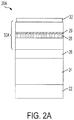
- Structure 20A comprises a standard sapphire (Al 2 O 3 ) or GaN substrate 22, on which is formed a GaN template layer 24.
- the active region 28 comprises a relatively conventional InGaN multiple-quantum-well (MQW) adjusted for 500 nm emission, for example with In composition in the range of 25-30%.
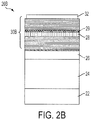
- MQW 28 is embedded in an InGaN separate confinement heterostructure (SCH) 30.
- InGaN SCH may be bulk material 30A, shown in Fig.
- SPSL InGaN short-period superlattice
- the structure is provided with a transverse waveguide which is asymmetric across the active region.
- an alternative cladding layer 32 is provided.
- Cladding layer 32 has a number of unique criteria. First, is it highly optically reflective at the wavelength of operation of the active layer. This may be quantified, for example, by examining the complex index of refraction of the selected material. Second, the material is relatively highly conductive. This may be quantified, for example, by examining the bulk resistivity of the selected material. While the actual material selected for cladding layer 32 will vary from application to application, one example discussed further below which meets these criteria is metallic silver.
- the n-side of the laser structure may optionally include an n-AlGaN layer 26 to serve as a cladding layer.
- the AIGaN layer is optional due to the thick GaN substrate/template which itself may serve as a lower cladding layer. Whether the additional n-AlGaN layer 26 is provided or not, it will now be appreciated that the lower and upper cladding layers are of different materials, and very likely of different thicknesses, even though the cladding pair provide waveguiding in the plane of the layers (i.e., transverse waveguiding). Accordingly, we refer to this system as an asymmetric transverse waveguide.
- n ⁇ n + i ⁇
- n the real portion or refractive index
- ⁇ the imaginary portion or extinction coefficient
- n i and ⁇ i are the refractive index and the extinction coefficient, respectively, of the material from where light is incident from.
- the cladding reflectivity seen by the guided wave depends on the "direction vector" of the guided wave. Nevertheless, the reflectivity at normal incidence, R, is a simple and convenient measure that can be used when selecting materials for the cladding layer. Once chosen, the actual performance of the selected material as a cladding layer should then be evaluated by numerical simulation of the waveguide.
- a desirable cladding material should exhibit a high reflectivity. If this condition is satisfied, the optical mode experiences only a very small penetration into the material, and low modal loss can be achieved even if the cladding material has a high extinction coefficient.
- a candidate cladding material that has a very small real component of the complex index will have a large refractive index mismatch with respect to the semiconductor. Since the mismatch appears on the numerator of the expression for R, such a material would be a promising candidate for providing the desired high reflectivity because a high normal incidence reflectivity correlates with a high guided mode reflectivity. Silver, for example, would be a promising candidate for the cladding material because it has a low refractive index.
- Cladding layer 32 also serves as an ohmic contact, and therefore relatively low bulk resistance is required.
- Certain high work-function metals are one category of materials with desirable low electrical resistance.
- most high-work-function metals e.g., Pd, Pt, Ni
- Pd, Pt, Ni high-work-function metals
- they are very optically lossy, so that for conventional nitride LD structures a sufficiently thick p-cladding layer must be grown over the active region in order to contain the evanescent tail of the mode and thereby suppress its overlap with the absorptive metal.
- Silver is an exception, as its real index n is low throughout the entire visible spectrum.
- silver is one material satisfying the low optical loss, high conductivity requirements so as to be substitute for the p-type semiconductor cladding layer. Indeed, such a material may also function as the upper p-contact for the device.
- Fig. 3 is a plot of the complex index, ⁇ , values for silver.
- the real component, n of silver's complex index is very small (below about 0.3 for wavelengths above 350 nm, particularly in the range of about 480 -550 nm), extending through the entire visible spectrum.
- n the complex index of silver's complex index
- a Ag-clad LD structure of the composition shown in Fig. 2 was simulated. The simulation was for a device operating at a wavelength of 500 nm.
- Table 1 tabulates the normal incident reflectivity of silver and nickel for light propagating from a GaN layer. Note that Ag is a much better reflector than Ni for wavelengths ranging from 365 nm to 530 nm. Therefore, Ag is a good choice for a cladding material in the GaN system. Other cladding material choices may be suitable for other wavelengths in other material systems, such as the red or near infra-red wavelengths in the GaAs or InP systems.
- n Ag 0.13 + 2.95i In 0.10 Ga 0.90 N p-SCH (54)
- Transverse guided-mode simulations were performed for this silver-clad structure.
- the optical confinement factor ( ⁇ ) and the mode loss ( ⁇ ) due to the silver cladding/p-contact were determined.
- the tradeoff between ⁇ and ⁇ was examined, and the structural parameters were adjusted to optimize this tradeoff.
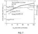
- the In 0.1 GaN lower-and upper-SCH layers46, 54 were adjusted to maximize the optical confinement factor value, and the loss and ⁇ values were evaluated for several different Al 0.07 GaN lower cladding layer 44 thicknesses. All simulations assumed a wavelength of 500 nm. It should be appreciated that, the results of this investigation also translate to any wavelength for which silver is a strong reflector, i.e., ⁇ > 350 nm, as shown by its dispersion characteristic in Fig. 3 .
- Fig. 5 shows the aggregate ⁇ value, ⁇ total , for a conventional 405 nm laser, as a function of the number of 3 nm InGaN QWs.
- ⁇ is ⁇ 4%, or 1% per QW.
- the ⁇ total values for the 4QW, 500 nm LD with silver cladding are also represented. Five points are shown, corresponding to the cases of different Al 0.07 GaN lower cladding layer thicknesses, including 0 nm (i.e., no AIGaN lower cladding layer), 250 nm, 500 nm, and 1000 nm thickness. Also shown are the data for a 250 nm thick lower cladding layer of Al 0.15 GaN.
- the largest thickness represents the approximate strain limit for a film grown epitaxially on a GaN template.
- the SCH layer thicknesses are adjusted to give the maximum ⁇ total value.
- the optimum values for the SCH thickness will ultimately depend on the tradeoffs between ⁇ total , ⁇ metal , and the gain-current characteristic of the QW gain medium.
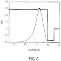
- An example of the transverse near-field mode intensity profile is shown in Fig. 6 for the case of no AIGaN lower cladding layer (i.e., the lower cladding is entirely GaN).
- ⁇ total and the mode loss due to the metal cladding are indicated in Table 3, below, along with the In 0.1 GaN SCH thicknesses that maximize ⁇ total .
- these ⁇ total and ⁇ metal values are plotted in Fig. 7 .
- the values for a conventional 405 nm 4 x 3 nm In 0.1 GaN QW LD are also indicated (dashed lines in Fig. 7 ).
- the Ag-clad 500 nm LD structure has somewhat lower ⁇ total , and significantly greater loss, attributed to the metal.
- Including an AIGaN lower cladding layer contributes greater confinement for higher ⁇ , but it also causes a significant increase in loss due to absorption by the silver-metal cladding layer on the opposite side of the waveguide.
- the lowest ⁇ metal loss is achieved for the AlGaN-free structure. While the loss is higher than that of a conventional 405 nm laser, the total loss for the Ag-clad structure compares more favorably with that of a conventional 405nm LD.
- the Ag-clad structure offers acceptable ⁇ total and ⁇ metal values. Additional optimization of other structural parameters (SCH composition, graded compositions, doping profile, etc.) may lead to further improvement. Most importantly, this is accomplished without AlGaInN cladding layers. Thus, the Ag-clad structure is well targeted to longer wavelength devices (e.g., green LDs), particularly because excessive strain may limit the practicality of conventional structures. But again, it must be realized that the asymmetric cladding, with the upper cladding being optically reflective and electrically conductive, is also applicable at shorter wavelengths.
- the mode loss may be further reduced by inclusion of a phase matching layer 62 between the metal and the p-type semiconductor surface.
- a transparent conductor such as indium-tin-oxide (ITO) could be used as the phase matching layer.
- Other transparent conductors are also viable, for example zinc oxide (ZnO) or indium zinc oxide (IZO).
- ZnO zinc oxide
- IZO indium zinc oxide
- the dispersion characteristics in Fig. 9 represent the n (solid curves) and ⁇ (dashed curves) values for an ITO film analyzed assuming two components: a portion near the deposition interface ("bottom", single curve), and the top of the film ("top", double curve).
- the real part of ITO's refractive index is about 2, or a few tenths less than that of GaN, and its imaginary component is much smaller than for a metal. Consequently, for a structure with a composite ITO+Ag cladding layer, the mode loss may be reduced compared to a metal-only cladding layer.
- this structure is additionally advantageous because it separates the ohmic contact function from the waveguide cladding-layer function.
- these two requirements often conflict and must be traded-off against each other, i.e., it is difficult to find a metal which offers both the requisite high work function and low mode loss.
- ITO serves as the ohmic contact, and the choice of overlying metal is not so limited to metals such as silver, which have a high work function. Rather, a much wider range of reflective materials becomes viable, so long as the material properties allow for a low modal absorption loss.
- one embodiment incorporates ITO and n- and p-SCH layers whose thicknesses and compositions are adjusted to maximize the ⁇ total value and/or minimize the mode loss ⁇ .
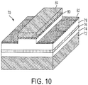
- a structure 70 incorporating ridge waveguides may also be constructed from this silver or Ag+ITO clad structure, as shown in Fig. 10 .
- a substrate not shown
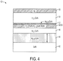
- an n-AlGaN lower cladding layer 72 is formed.
- An active region 76 of the type previously described is formed between lower n-InGaN SCH 74 and upper p-InGaN 78.
- a region of ITO is then deposited and patterned to form a ridge structure 80, then a passivation layer 82 such as of SiNx is deposited.
- an upper cladding layer 84 such as silver metal is deposited.
- a positive lateral index guide is formed by etching away a portion of the upper p-SCH outside the laser stripe. For example, by etching away 50 nm of the p-SCH from the optimized Ag+ITO-clad 500 nm structure described in Table 4, above (i.e., reducing its thickness from 218 nm to 168 nm), the mode effective index is depressed by approximately 0.005. This is a reasonable value for forming a single-mode waveguide, and typical of conventional ridge waveguides. Accordingly, the ridge width and etch-depth (which determines the lateral index step) should be optimized in the normal manner, to give the following performance characteristics:
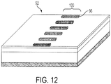
- the Ag-clad structure forms a distributed feedback (DFB) or distributed Bragg reflector (DBR) laser.
- a metal cladding layer 94 is formed as a grating of periodic stripes 96 of silver metal, or Ag+ITO. This structure may be formed over a lateral ridge waveguide 98, as shown in Figs. 11A and 11B , or the current injection may define a gain-guided stripe 100 as shown in Fig. 12 .
- the metal grating provides complex coupling (i.e., periodic index variation accompanied by a gain/loss modulation) that favors single-mode operation.
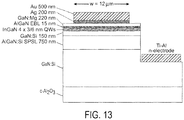
- a 412 nm 4 x 3nm In 0.1 Ga 0.9 N quantum well nitride laser diode in which the upper cladding layer is silver metal has been demonstrated.
- the Ag-clad nitride LD structure is shown in Fig. 13 .
- the n-side is similar to conventional GaN-based LDs, including a 750 nm Al 0.14 Ga 0.86 N/GaN (3/3 nm), (0001)-oriented short-period superlattice cladding layer deposited over a thick n-type GaN/sapphire template.
- the active region consists of 4 x In 0.1 Ga 0.9 N/GaN (3/6 nm) quantum wells, embedded in a GaN separate confinement heterostructure (SCH).
- a p-type Al 0.2 Ga 0.8 N:Mg electron blocking layer is deposited over the last GaN barrier.
- the silver metal cladding is applied directly over the p-type SCH layer, replacing the p-type AIGaN cladding layer typical of conventional nitride LD structures.
- the thicknesses of the n- and p-type SCH layers are designed through transverse waveguide simulations, to determine the QW confinement factor ( ⁇ ) and the mode loss ( ⁇ ) associated with the silver metal cladding, for the fundamental TE mode.
- the nitride LD heterostructure was prepared by metalorganic chemical vapor deposition (MOCVD) using trimethyl-group-III precursors, ammonia, silane and biscyclopentadienylmagnesium for n- and p-type doping, in H 2 and N 2 carrier gases.
- MOCVD metalorganic chemical vapor deposition
- the n-type AIGaN cladding layer was deposited at a pressure of 200 Torr, while all other layers were grown at an elevated pressure of 700 Torr for best optical efficiency and p-type doping.
- mirrors and n-contact pads were formed by chemically-assisted ion-beam etching (CAIBE).
- the silver cladding was formed by evaporating 200 nm silver, followed by 500 nm gold.
- the n-contact electrode was formed with a Ti-Au metallization. Cavity lengths were 300, 400, 500, 700, 1000, and 1500 ⁇ m, with uncoated (as-etched) mirrors; and the stripe width of the simple gain-guided LDs was 12 ⁇ m.
- the diodes were tested under pulsed conditions at room temperature, with 100 nsec pulse width, and 1 kHz repletion rate.
- the pulsed light vs. current characteristic for a 12 ⁇ m x 1000 ⁇ m stripe is shown in Fig. 14 .
- the threshold current is 1.4 A, corresponding to a threshold current density of about 12 kA/cm 2 .
- a far-field pattern emerged (with interference fringes produced by reflection from the etched surfaces in front of the mirror), indicative of spatial coherence and lasing.
- the lasing wavelength at 1.5 A pulsed current was 412 nm, as indicated in the spectrum shown in Fig. 15 .
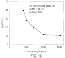
- the cavity-length dependence of threshold current density (J th ) is likewise shown in Fig. 16 .
- J th is relatively insensitive to length, due to the dominance of the distributed loss ⁇ ; while for short cavities J th is very high, due to the changing mirror loss combined with the sublinear gain vs. current characteristic typical of QWs.
- this cavity-length dependence of J th is roughly consistent with the estimated mode loss of about 30 cm -1 .
- the lowest measured J th was about 10 kA/cm 2 , for a 1500 ⁇ m cavity.
- the silver-clad LD heterostructure offers several advantages over conventional structures.
- the InGaN QW quality may be preserved against any degradation associated with the time/temperature exposure which would otherwise occur during growth of a thick p-AlGaN cladding layer. This benefit is especially significant for high-indium content structures, due to the inherent thermal instability of InGaN.
- the overall mode loss may be made acceptably small. Indeed, although the loss arising from absorption in the metal clad/contact is greater than that of a conventional nitride LD structure, the large asymmetry in the mode leads to lower loss from the mode's overlap with the p-type (Mg-doped) layers. Thereby, the overall distributed loss is within practical limits. And for long wavelength (blue-green) nitride LDs, the mode loss resulting from the silver metal may be further reduced by introduction of an ITO layer between the p-SCH and the silver.
Landscapes
- Physics & Mathematics (AREA)
- Optics & Photonics (AREA)
- Condensed Matter Physics & Semiconductors (AREA)
- General Physics & Mathematics (AREA)
- Electromagnetism (AREA)
- Engineering & Computer Science (AREA)
- Nanotechnology (AREA)
- Chemical & Material Sciences (AREA)
- Biophysics (AREA)
- Crystallography & Structural Chemistry (AREA)
- Life Sciences & Earth Sciences (AREA)
- Geometry (AREA)
- Semiconductor Lasers (AREA)
Applications Claiming Priority (1)
| Application Number | Priority Date | Filing Date | Title |
|---|---|---|---|
| US12/237,106 US7856040B2 (en) | 2008-09-24 | 2008-09-24 | Semiconductor light emitting devices with non-epitaxial upper cladding |
Publications (2)
| Publication Number | Publication Date |
|---|---|
| EP2169791A1 EP2169791A1 (en) | 2010-03-31 |
| EP2169791B1 true EP2169791B1 (en) | 2018-04-25 |
Family
ID=41381957
Family Applications (1)
| Application Number | Title | Priority Date | Filing Date |
|---|---|---|---|
| EP09170496.5A Not-in-force EP2169791B1 (en) | 2008-09-24 | 2009-09-17 | Semiconductor light emitting devices with non-epitaxial upper cladding |
Country Status (3)
| Country | Link |
|---|---|
| US (2) | US7856040B2 (enExample) |
| EP (1) | EP2169791B1 (enExample) |
| JP (2) | JP2010080960A (enExample) |
Families Citing this family (21)
| Publication number | Priority date | Publication date | Assignee | Title |
|---|---|---|---|---|
| US7856040B2 (en) | 2008-09-24 | 2010-12-21 | Palo Alto Research Center Incorporated | Semiconductor light emitting devices with non-epitaxial upper cladding |
| EP2556572A1 (en) * | 2010-04-05 | 2013-02-13 | The Regents of the University of California | Aluminum gallium nitride barriers and separate confinement heterostructure (sch) layers for semipolar plane iii-nitride semiconductor-based light emitting diodes and laser diodes |
| US9012948B2 (en) * | 2010-10-04 | 2015-04-21 | Epistar Corporation | Light-emitting element having a plurality of contact parts |
| JP2012186195A (ja) * | 2011-03-03 | 2012-09-27 | Toshiba Corp | 半導体発光素子及びその製造方法 |
| JP5479391B2 (ja) * | 2011-03-08 | 2014-04-23 | 株式会社東芝 | 半導体発光素子及びその製造方法 |
| JP5963004B2 (ja) * | 2011-03-24 | 2016-08-03 | パナソニックIpマネジメント株式会社 | 窒化物半導体発光素子 |
| US8748919B2 (en) | 2011-04-28 | 2014-06-10 | Palo Alto Research Center Incorporated | Ultraviolet light emitting device incorporating optically absorbing layers |
| DE102011077542B4 (de) * | 2011-06-15 | 2020-06-18 | Osram Opto Semiconductors Gmbh | Optoelektronischer halbleiterkörper und verfahren zur herstellung eines optoelektronischen halbleiterkörpers |
| KR101946005B1 (ko) * | 2012-01-26 | 2019-02-08 | 삼성전자주식회사 | 그래핀 소자 및 그 제조방법 |
| US9401452B2 (en) * | 2012-09-14 | 2016-07-26 | Palo Alto Research Center Incorporated | P-side layers for short wavelength light emitters |
| CN104078837B (zh) * | 2013-03-29 | 2017-12-15 | 山东华光光电子股份有限公司 | 一种GaN基蓝绿光激光二极管器件及制作方法 |
| WO2015052861A1 (ja) * | 2013-10-10 | 2015-04-16 | パナソニックIpマネジメント株式会社 | 半導体発光装置 |
| CN103887705A (zh) * | 2014-03-13 | 2014-06-25 | 中国科学院半导体研究所 | 金属完全限制的硅基混合激光器的制备方法 |
| FR3026571B1 (fr) * | 2014-09-26 | 2016-12-02 | Thales Sa | Procede d'elaboration d'une structure resonante d'un laser a semi-conducteur a contre-reaction repartie |
| KR101968215B1 (ko) * | 2015-03-16 | 2019-04-11 | 주식회사 엘지화학 | 전도성 구조체 및 이를 포함하는 전자 소자 |
| CN105589119A (zh) * | 2016-02-29 | 2016-05-18 | 中国科学院半导体研究所 | 带有dbr层的太赫兹光电导天线外延结构及制备方法 |
| US10056735B1 (en) * | 2016-05-23 | 2018-08-21 | X Development Llc | Scanning UV light source utilizing semiconductor heterostructures |
| CN107086259A (zh) * | 2017-05-24 | 2017-08-22 | 广西师范大学 | 基于表面等离子波导的新型发光二极管 |
| DE102017113389B4 (de) | 2017-06-19 | 2021-07-29 | OSRAM Opto Semiconductors Gesellschaft mit beschränkter Haftung | Halbleiterlaserdiode |
| US11133649B2 (en) * | 2019-06-21 | 2021-09-28 | Palo Alto Research Center Incorporated | Index and gain coupled distributed feedback laser |
| CN114792929A (zh) * | 2021-11-18 | 2022-07-26 | 埃特曼(北京)半导体技术有限公司 | 激光器制备方法及激光器 |
Family Cites Families (24)
| Publication number | Priority date | Publication date | Assignee | Title |
|---|---|---|---|---|
| US4639922A (en) * | 1984-09-28 | 1987-01-27 | Bell Communications Research, Inc. | Single mode injection laser structure |
| JPS62189785A (ja) | 1986-02-17 | 1987-08-19 | Kokusai Denshin Denwa Co Ltd <Kdd> | 分布ブラツグ反射器を有する半導体装置 |
| JPH08288592A (ja) * | 1995-04-14 | 1996-11-01 | Oki Electric Ind Co Ltd | 集積化半導体光デバイスおよびその製造方法 |
| JP3464853B2 (ja) * | 1995-09-06 | 2003-11-10 | 株式会社東芝 | 半導体レーザ |
| JP3576764B2 (ja) * | 1996-09-17 | 2004-10-13 | 株式会社東芝 | グレーティング結合型面発光装置 |
| JP3717255B2 (ja) * | 1996-12-26 | 2005-11-16 | 豊田合成株式会社 | 3族窒化物半導体レーザ素子 |
| JPH11220212A (ja) * | 1998-02-02 | 1999-08-10 | Toshiba Corp | 光素子、光素子の駆動方法及び半導体レーザ素子 |
| JPH11274642A (ja) * | 1998-03-19 | 1999-10-08 | Toshiba Corp | 半導体発光素子及びその製造方法 |
| JP2000236142A (ja) * | 1998-12-15 | 2000-08-29 | Nichia Chem Ind Ltd | 窒化物半導体レーザ素子 |
| JP4306037B2 (ja) * | 1999-08-11 | 2009-07-29 | 昭和電工株式会社 | Iii族窒化物半導体発光素子 |
| JP4804618B2 (ja) * | 2000-09-28 | 2011-11-02 | 富士通株式会社 | 半導体レーザ |
| US6724013B2 (en) * | 2001-12-21 | 2004-04-20 | Xerox Corporation | Edge-emitting nitride-based laser diode with p-n tunnel junction current injection |
| JP4076145B2 (ja) * | 2003-02-26 | 2008-04-16 | 日本電信電話株式会社 | 複素結合型分布帰還型半導体レーザ |
| US7123637B2 (en) | 2003-03-20 | 2006-10-17 | Xerox Corporation | Nitride-based laser diode with GaN waveguide/cladding layer |
| US6990132B2 (en) * | 2003-03-20 | 2006-01-24 | Xerox Corporation | Laser diode with metal-oxide upper cladding layer |
| KR20050082251A (ko) | 2004-02-18 | 2005-08-23 | 삼성전자주식회사 | 반도체 레이저 디바이스 |
| JP4909533B2 (ja) * | 2004-06-21 | 2012-04-04 | パナソニック株式会社 | 半導体レーザ素子及びその製造方法 |
| US7279751B2 (en) | 2004-06-21 | 2007-10-09 | Matsushita Electric Industrial Co., Ltd. | Semiconductor laser device and manufacturing method thereof |
| KR100657909B1 (ko) * | 2004-11-08 | 2006-12-14 | 삼성전기주식회사 | 화합물 반도체 소자의 전극 형성방법 |
| JP4179280B2 (ja) * | 2004-12-28 | 2008-11-12 | ソニー株式会社 | 半導体発光素子の製造方法 |
| KR101124290B1 (ko) * | 2005-11-03 | 2012-03-27 | 삼성엘이디 주식회사 | 질화물 반도체 레이저 소자 및 그 제조 방법 |
| JP5444609B2 (ja) * | 2007-11-08 | 2014-03-19 | 日亜化学工業株式会社 | 半導体レーザ素子 |
| JP2010016261A (ja) * | 2008-07-04 | 2010-01-21 | Sharp Corp | 窒化物半導体レーザ素子 |
| US7856040B2 (en) | 2008-09-24 | 2010-12-21 | Palo Alto Research Center Incorporated | Semiconductor light emitting devices with non-epitaxial upper cladding |
-
2008
- 2008-09-24 US US12/237,106 patent/US7856040B2/en not_active Expired - Fee Related
-
2009
- 2009-09-16 JP JP2009214461A patent/JP2010080960A/ja active Pending
- 2009-09-17 EP EP09170496.5A patent/EP2169791B1/en not_active Not-in-force
-
2010
- 2010-11-08 US US12/941,862 patent/US8023544B2/en not_active Expired - Fee Related
-
2015
- 2015-02-26 JP JP2015036177A patent/JP2015099944A/ja active Pending
Non-Patent Citations (1)
| Title |
|---|
| None * |
Also Published As
| Publication number | Publication date |
|---|---|
| US7856040B2 (en) | 2010-12-21 |
| JP2010080960A (ja) | 2010-04-08 |
| EP2169791A1 (en) | 2010-03-31 |
| US20110051768A1 (en) | 2011-03-03 |
| JP2015099944A (ja) | 2015-05-28 |
| US8023544B2 (en) | 2011-09-20 |
| US20100074292A1 (en) | 2010-03-25 |
Similar Documents
| Publication | Publication Date | Title |
|---|---|---|
| EP2169791B1 (en) | Semiconductor light emitting devices with non-epitaxial upper cladding | |
| TWI418106B (zh) | 半導體發光元件 | |
| EP2957004B1 (en) | Single-step-grown transversely coupled distributed feedback laser | |
| JP2002531959A (ja) | 光電式デバイスのための化合物半導体構造 | |
| CN102856788A (zh) | 二分型半导体激光元件及其制造方法、以及其驱动方法 | |
| US7362788B2 (en) | Semiconductor laser and fabricating method thereof | |
| US20070223549A1 (en) | High-Power Optoelectronic Device with Improved Beam Quality Incorporating A Lateral Mode Filtering Section | |
| EP1162708A1 (en) | Distributed feedback semiconductor laser device | |
| EP3304660A1 (en) | Interband cascade lasers with low-fill factor top contact for reduced loss | |
| Bulashevich et al. | Effect of free-carrier absorption on performance of 808 nm AlGaAs-based high-power laser diodes | |
| EP2575221A2 (en) | Light-emitting device and method of manufacturing the same | |
| EP1289082A2 (en) | Semiconductor laser device having selective absorption qualities over a wide temperature range | |
| JP2013074001A (ja) | 発光素子及びその製造方法 | |
| US8023546B2 (en) | Semiconductor laser with integrated contact and waveguide | |
| JP2019079911A (ja) | 半導体レーザ素子 | |
| JP2003133636A (ja) | 分布帰還型半導体レーザ素子 | |
| Bour et al. | Silver-clad nitride semiconductor laser diode | |
| Cheng et al. | Nitride laser diodes with nonepitaxial cladding layers | |
| JP4163343B2 (ja) | 発光素子および発光素子モジュール | |
| JP2004103679A (ja) | 半導体発光素子および半導体発光素子モジュール | |
| JP2000236141A (ja) | 半導体発光素子 | |
| CA2357974C (en) | Semiconductor laser device and optical fiber amplifier using the same | |
| JPH07162085A (ja) | 半導体発光装置 | |
| JP2007273901A (ja) | 半導体発光素子 | |
| Bulashevich et al. | Effect of Free-Carrier Absorption on Performance of 808 nm High-Power Laser Diodes |
Legal Events
| Date | Code | Title | Description |
|---|---|---|---|
| PUAI | Public reference made under article 153(3) epc to a published international application that has entered the european phase |
Free format text: ORIGINAL CODE: 0009012 |
|
| AK | Designated contracting states |
Kind code of ref document: A1 Designated state(s): AT BE BG CH CY CZ DE DK EE ES FI FR GB GR HR HU IE IS IT LI LT LU LV MC MK MT NL NO PL PT RO SE SI SK SM TR |
|
| AX | Request for extension of the european patent |
Extension state: AL BA RS |
|
| 17P | Request for examination filed |
Effective date: 20100930 |
|
| 17Q | First examination report despatched |
Effective date: 20101025 |
|
| REG | Reference to a national code |
Ref country code: DE Ref legal event code: R079 Ref document number: 602009051943 Country of ref document: DE Free format text: PREVIOUS MAIN CLASS: H01S0005343000 Ipc: H01S0005320000 |
|
| RIC1 | Information provided on ipc code assigned before grant |
Ipc: H01S 5/042 20060101ALI20171005BHEP Ipc: H01S 5/22 20060101ALN20171005BHEP Ipc: H01S 5/32 20060101AFI20171005BHEP Ipc: H01S 5/20 20060101ALN20171005BHEP Ipc: H01S 5/343 20060101ALI20171005BHEP Ipc: H01S 5/10 20060101ALN20171005BHEP Ipc: H01L 33/00 20100101ALN20171005BHEP Ipc: H01S 5/12 20060101ALN20171005BHEP |
|
| GRAP | Despatch of communication of intention to grant a patent |
Free format text: ORIGINAL CODE: EPIDOSNIGR1 |
|
| INTG | Intention to grant announced |
Effective date: 20171117 |
|
| GRAA | (expected) grant |
Free format text: ORIGINAL CODE: 0009210 |
|
| GRAS | Grant fee paid |
Free format text: ORIGINAL CODE: EPIDOSNIGR3 |
|
| AK | Designated contracting states |
Kind code of ref document: B1 Designated state(s): AT BE BG CH CY CZ DE DK EE ES FI FR GB GR HR HU IE IS IT LI LT LU LV MC MK MT NL NO PL PT RO SE SI SK SM TR |
|
| REG | Reference to a national code |
Ref country code: GB Ref legal event code: FG4D |
|
| REG | Reference to a national code |
Ref country code: CH Ref legal event code: EP |
|
| REG | Reference to a national code |
Ref country code: AT Ref legal event code: REF Ref document number: 993842 Country of ref document: AT Kind code of ref document: T Effective date: 20180515 |
|
| REG | Reference to a national code |
Ref country code: IE Ref legal event code: FG4D |
|
| REG | Reference to a national code |
Ref country code: DE Ref legal event code: R096 Ref document number: 602009051943 Country of ref document: DE |
|
| REG | Reference to a national code |
Ref country code: NL Ref legal event code: MP Effective date: 20180425 |
|
| REG | Reference to a national code |
Ref country code: LT Ref legal event code: MG4D |
|
| PG25 | Lapsed in a contracting state [announced via postgrant information from national office to epo] |
Ref country code: NL Free format text: LAPSE BECAUSE OF FAILURE TO SUBMIT A TRANSLATION OF THE DESCRIPTION OR TO PAY THE FEE WITHIN THE PRESCRIBED TIME-LIMIT Effective date: 20180425 |
|
| PG25 | Lapsed in a contracting state [announced via postgrant information from national office to epo] |
Ref country code: ES Free format text: LAPSE BECAUSE OF FAILURE TO SUBMIT A TRANSLATION OF THE DESCRIPTION OR TO PAY THE FEE WITHIN THE PRESCRIBED TIME-LIMIT Effective date: 20180425 Ref country code: FI Free format text: LAPSE BECAUSE OF FAILURE TO SUBMIT A TRANSLATION OF THE DESCRIPTION OR TO PAY THE FEE WITHIN THE PRESCRIBED TIME-LIMIT Effective date: 20180425 Ref country code: SE Free format text: LAPSE BECAUSE OF FAILURE TO SUBMIT A TRANSLATION OF THE DESCRIPTION OR TO PAY THE FEE WITHIN THE PRESCRIBED TIME-LIMIT Effective date: 20180425 Ref country code: NO Free format text: LAPSE BECAUSE OF FAILURE TO SUBMIT A TRANSLATION OF THE DESCRIPTION OR TO PAY THE FEE WITHIN THE PRESCRIBED TIME-LIMIT Effective date: 20180725 Ref country code: LT Free format text: LAPSE BECAUSE OF FAILURE TO SUBMIT A TRANSLATION OF THE DESCRIPTION OR TO PAY THE FEE WITHIN THE PRESCRIBED TIME-LIMIT Effective date: 20180425 Ref country code: PL Free format text: LAPSE BECAUSE OF FAILURE TO SUBMIT A TRANSLATION OF THE DESCRIPTION OR TO PAY THE FEE WITHIN THE PRESCRIBED TIME-LIMIT Effective date: 20180425 Ref country code: BG Free format text: LAPSE BECAUSE OF FAILURE TO SUBMIT A TRANSLATION OF THE DESCRIPTION OR TO PAY THE FEE WITHIN THE PRESCRIBED TIME-LIMIT Effective date: 20180725 |
|
| PG25 | Lapsed in a contracting state [announced via postgrant information from national office to epo] |
Ref country code: GR Free format text: LAPSE BECAUSE OF FAILURE TO SUBMIT A TRANSLATION OF THE DESCRIPTION OR TO PAY THE FEE WITHIN THE PRESCRIBED TIME-LIMIT Effective date: 20180726 Ref country code: HR Free format text: LAPSE BECAUSE OF FAILURE TO SUBMIT A TRANSLATION OF THE DESCRIPTION OR TO PAY THE FEE WITHIN THE PRESCRIBED TIME-LIMIT Effective date: 20180425 Ref country code: LV Free format text: LAPSE BECAUSE OF FAILURE TO SUBMIT A TRANSLATION OF THE DESCRIPTION OR TO PAY THE FEE WITHIN THE PRESCRIBED TIME-LIMIT Effective date: 20180425 |
|
| REG | Reference to a national code |
Ref country code: AT Ref legal event code: MK05 Ref document number: 993842 Country of ref document: AT Kind code of ref document: T Effective date: 20180425 |
|
| PG25 | Lapsed in a contracting state [announced via postgrant information from national office to epo] |
Ref country code: PT Free format text: LAPSE BECAUSE OF FAILURE TO SUBMIT A TRANSLATION OF THE DESCRIPTION OR TO PAY THE FEE WITHIN THE PRESCRIBED TIME-LIMIT Effective date: 20180827 |
|
| REG | Reference to a national code |
Ref country code: DE Ref legal event code: R097 Ref document number: 602009051943 Country of ref document: DE |
|
| PG25 | Lapsed in a contracting state [announced via postgrant information from national office to epo] |
Ref country code: RO Free format text: LAPSE BECAUSE OF FAILURE TO SUBMIT A TRANSLATION OF THE DESCRIPTION OR TO PAY THE FEE WITHIN THE PRESCRIBED TIME-LIMIT Effective date: 20180425 Ref country code: SK Free format text: LAPSE BECAUSE OF FAILURE TO SUBMIT A TRANSLATION OF THE DESCRIPTION OR TO PAY THE FEE WITHIN THE PRESCRIBED TIME-LIMIT Effective date: 20180425 Ref country code: CZ Free format text: LAPSE BECAUSE OF FAILURE TO SUBMIT A TRANSLATION OF THE DESCRIPTION OR TO PAY THE FEE WITHIN THE PRESCRIBED TIME-LIMIT Effective date: 20180425 Ref country code: EE Free format text: LAPSE BECAUSE OF FAILURE TO SUBMIT A TRANSLATION OF THE DESCRIPTION OR TO PAY THE FEE WITHIN THE PRESCRIBED TIME-LIMIT Effective date: 20180425 Ref country code: AT Free format text: LAPSE BECAUSE OF FAILURE TO SUBMIT A TRANSLATION OF THE DESCRIPTION OR TO PAY THE FEE WITHIN THE PRESCRIBED TIME-LIMIT Effective date: 20180425 Ref country code: DK Free format text: LAPSE BECAUSE OF FAILURE TO SUBMIT A TRANSLATION OF THE DESCRIPTION OR TO PAY THE FEE WITHIN THE PRESCRIBED TIME-LIMIT Effective date: 20180425 |
|
| PG25 | Lapsed in a contracting state [announced via postgrant information from national office to epo] |
Ref country code: IT Free format text: LAPSE BECAUSE OF FAILURE TO SUBMIT A TRANSLATION OF THE DESCRIPTION OR TO PAY THE FEE WITHIN THE PRESCRIBED TIME-LIMIT Effective date: 20180425 Ref country code: SM Free format text: LAPSE BECAUSE OF FAILURE TO SUBMIT A TRANSLATION OF THE DESCRIPTION OR TO PAY THE FEE WITHIN THE PRESCRIBED TIME-LIMIT Effective date: 20180425 |
|
| PLBE | No opposition filed within time limit |
Free format text: ORIGINAL CODE: 0009261 |
|
| STAA | Information on the status of an ep patent application or granted ep patent |
Free format text: STATUS: NO OPPOSITION FILED WITHIN TIME LIMIT |
|
| REG | Reference to a national code |
Ref country code: DE Ref legal event code: R119 Ref document number: 602009051943 Country of ref document: DE |
|
| 26N | No opposition filed |
Effective date: 20190128 |
|
| PG25 | Lapsed in a contracting state [announced via postgrant information from national office to epo] |
Ref country code: MC Free format text: LAPSE BECAUSE OF FAILURE TO SUBMIT A TRANSLATION OF THE DESCRIPTION OR TO PAY THE FEE WITHIN THE PRESCRIBED TIME-LIMIT Effective date: 20180425 |
|
| REG | Reference to a national code |
Ref country code: CH Ref legal event code: PL |
|
| GBPC | Gb: european patent ceased through non-payment of renewal fee |
Effective date: 20180917 |
|
| PG25 | Lapsed in a contracting state [announced via postgrant information from national office to epo] |
Ref country code: SI Free format text: LAPSE BECAUSE OF FAILURE TO SUBMIT A TRANSLATION OF THE DESCRIPTION OR TO PAY THE FEE WITHIN THE PRESCRIBED TIME-LIMIT Effective date: 20180425 |
|
| REG | Reference to a national code |
Ref country code: BE Ref legal event code: MM Effective date: 20180930 |
|
| REG | Reference to a national code |
Ref country code: IE Ref legal event code: MM4A |
|
| PG25 | Lapsed in a contracting state [announced via postgrant information from national office to epo] |
Ref country code: LU Free format text: LAPSE BECAUSE OF NON-PAYMENT OF DUE FEES Effective date: 20180917 |
|
| PG25 | Lapsed in a contracting state [announced via postgrant information from national office to epo] |
Ref country code: DE Free format text: LAPSE BECAUSE OF NON-PAYMENT OF DUE FEES Effective date: 20190402 Ref country code: IE Free format text: LAPSE BECAUSE OF NON-PAYMENT OF DUE FEES Effective date: 20180917 |
|
| PG25 | Lapsed in a contracting state [announced via postgrant information from national office to epo] |
Ref country code: FR Free format text: LAPSE BECAUSE OF NON-PAYMENT OF DUE FEES Effective date: 20180930 Ref country code: BE Free format text: LAPSE BECAUSE OF NON-PAYMENT OF DUE FEES Effective date: 20180930 Ref country code: CH Free format text: LAPSE BECAUSE OF NON-PAYMENT OF DUE FEES Effective date: 20180930 Ref country code: LI Free format text: LAPSE BECAUSE OF NON-PAYMENT OF DUE FEES Effective date: 20180930 |
|
| PG25 | Lapsed in a contracting state [announced via postgrant information from national office to epo] |
Ref country code: GB Free format text: LAPSE BECAUSE OF NON-PAYMENT OF DUE FEES Effective date: 20180917 |
|
| PG25 | Lapsed in a contracting state [announced via postgrant information from national office to epo] |
Ref country code: MT Free format text: LAPSE BECAUSE OF NON-PAYMENT OF DUE FEES Effective date: 20180917 |
|
| PG25 | Lapsed in a contracting state [announced via postgrant information from national office to epo] |
Ref country code: TR Free format text: LAPSE BECAUSE OF FAILURE TO SUBMIT A TRANSLATION OF THE DESCRIPTION OR TO PAY THE FEE WITHIN THE PRESCRIBED TIME-LIMIT Effective date: 20180425 |
|
| PG25 | Lapsed in a contracting state [announced via postgrant information from national office to epo] |
Ref country code: HU Free format text: LAPSE BECAUSE OF FAILURE TO SUBMIT A TRANSLATION OF THE DESCRIPTION OR TO PAY THE FEE WITHIN THE PRESCRIBED TIME-LIMIT; INVALID AB INITIO Effective date: 20090917 |
|
| PG25 | Lapsed in a contracting state [announced via postgrant information from national office to epo] |
Ref country code: CY Free format text: LAPSE BECAUSE OF FAILURE TO SUBMIT A TRANSLATION OF THE DESCRIPTION OR TO PAY THE FEE WITHIN THE PRESCRIBED TIME-LIMIT Effective date: 20180425 Ref country code: MK Free format text: LAPSE BECAUSE OF NON-PAYMENT OF DUE FEES Effective date: 20180425 |
|
| PG25 | Lapsed in a contracting state [announced via postgrant information from national office to epo] |
Ref country code: IS Free format text: LAPSE BECAUSE OF FAILURE TO SUBMIT A TRANSLATION OF THE DESCRIPTION OR TO PAY THE FEE WITHIN THE PRESCRIBED TIME-LIMIT Effective date: 20180825 |