EP2075831A2 - Halbleitervorrichtung mit geteiltem Kontaktloch für Gate-Elektrode und Drain-Gebiet - Google Patents
Halbleitervorrichtung mit geteiltem Kontaktloch für Gate-Elektrode und Drain-Gebiet Download PDFInfo
- Publication number
- EP2075831A2 EP2075831A2 EP08254137A EP08254137A EP2075831A2 EP 2075831 A2 EP2075831 A2 EP 2075831A2 EP 08254137 A EP08254137 A EP 08254137A EP 08254137 A EP08254137 A EP 08254137A EP 2075831 A2 EP2075831 A2 EP 2075831A2
- Authority
- EP
- European Patent Office
- Prior art keywords
- gate electrode
- sidewall
- electrode layer
- contact hole
- shared contact
- Prior art date
- Legal status (The legal status is an assumption and is not a legal conclusion. Google has not performed a legal analysis and makes no representation as to the accuracy of the status listed.)
- Withdrawn
Links
Images















Classifications
-
- H—ELECTRICITY
- H10—SEMICONDUCTOR DEVICES; ELECTRIC SOLID-STATE DEVICES NOT OTHERWISE PROVIDED FOR
- H10B—ELECTRONIC MEMORY DEVICES
- H10B10/00—Static random access memory [SRAM] devices
- H10B10/12—Static random access memory [SRAM] devices comprising a MOSFET load element
-
- H—ELECTRICITY
- H10—SEMICONDUCTOR DEVICES; ELECTRIC SOLID-STATE DEVICES NOT OTHERWISE PROVIDED FOR
- H10B—ELECTRONIC MEMORY DEVICES
- H10B10/00—Static random access memory [SRAM] devices
-
- H—ELECTRICITY
- H10—SEMICONDUCTOR DEVICES; ELECTRIC SOLID-STATE DEVICES NOT OTHERWISE PROVIDED FOR
- H10D—INORGANIC ELECTRIC SEMICONDUCTOR DEVICES
- H10D64/00—Electrodes of devices having potential barriers
- H10D64/20—Electrodes characterised by their shapes, relative sizes or dispositions
- H10D64/27—Electrodes not carrying the current to be rectified, amplified, oscillated or switched, e.g. gates
- H10D64/311—Gate electrodes for field-effect devices
- H10D64/411—Gate electrodes for field-effect devices for FETs
- H10D64/511—Gate electrodes for field-effect devices for FETs for IGFETs
- H10D64/517—Gate electrodes for field-effect devices for FETs for IGFETs characterised by the conducting layers
- H10D64/519—Gate electrodes for field-effect devices for FETs for IGFETs characterised by the conducting layers characterised by their top-view geometrical layouts
-
- H—ELECTRICITY
- H10—SEMICONDUCTOR DEVICES; ELECTRIC SOLID-STATE DEVICES NOT OTHERWISE PROVIDED FOR
- H10D—INORGANIC ELECTRIC SEMICONDUCTOR DEVICES
- H10D84/00—Integrated devices formed in or on semiconductor substrates that comprise only semiconducting layers, e.g. on Si wafers or on GaAs-on-Si wafers
- H10D84/80—Integrated devices formed in or on semiconductor substrates that comprise only semiconducting layers, e.g. on Si wafers or on GaAs-on-Si wafers characterised by the integration of at least one component covered by groups H10D12/00 or H10D30/00, e.g. integration of IGFETs
-
- H—ELECTRICITY
- H10—SEMICONDUCTOR DEVICES; ELECTRIC SOLID-STATE DEVICES NOT OTHERWISE PROVIDED FOR
- H10D—INORGANIC ELECTRIC SEMICONDUCTOR DEVICES
- H10D89/00—Aspects of integrated devices not covered by groups H10D84/00 - H10D88/00
- H10D89/10—Integrated device layouts
-
- H—ELECTRICITY
- H10—SEMICONDUCTOR DEVICES; ELECTRIC SOLID-STATE DEVICES NOT OTHERWISE PROVIDED FOR
- H10W—GENERIC PACKAGES, INTERCONNECTIONS, CONNECTORS OR OTHER CONSTRUCTIONAL DETAILS OF DEVICES COVERED BY CLASS H10
- H10W20/00—Interconnections in chips, wafers or substrates
- H10W20/01—Manufacture or treatment
- H10W20/031—Manufacture or treatment of conductive parts of the interconnections
- H10W20/0698—Local interconnections
Definitions
- the present invention relates to a semiconductor device and a photomask, particularly to a semiconductor device having a shared contact hole that reaches both a gate electrode layer and an impurity region and a photomask that is used in patterning of the gate electrode layer.
- Japanese Patent Laying-Open Nos. 09-321152 , 2004-273642 , 2004-273972 , and 2004-327796 disclose the semiconductor device having the shared contact hole that reaches both the gate electrode layer and the impurity region.
- the shared contact hole has a tapered shape in section in which an opening diameter is decreased from an opening end toward a deep position. Therefore, when an etching film such as an insulator is etched to make the shared contact hole, an etching area of the etching film is reduced with the progress of etching. The reduction of the etching area obstructs the progress of the etching, resulting in a conductive problem such as an opening defect in which the shared contact hole does not reach an active layer (impurity region).
- the etching is obstructed in the middle of the etching by a projection of a sidewall spacer located in a gate electrode layer sidewall. Therefore, in a planar view, unless a distance from an end (end that is not etched by the etching in making the shared contact hole) of the sidewall spacer to an edge portion in a long-side direction of the shared contact hole is largely ensured, a residue is generated in a process of etching a liner nitride film on the sidewall spacer, thereby generating the opening defect.
- a preferred aim of the invention is to provide semiconductor device and a photomask that can suppress the opening defect of the shared contact hole.
- An aspect in accordance with the invention provides a semiconductor device including a semiconductor substrate having a main surface; an impurity region formed in the main surface; an insulated gate field effect transistor formed in the semiconductor substrate; and an insulator formed on the impurity region and the insulated gate field effect transistor.
- the insulated gate field effect transistor includes a pair of source/drain regions formed in the main surface; and a gate electrode layer formed on a channel formation region with a gate insulator interposed therebetween, the channel formation region being sandwiched between the pair of source/drain regions.
- the insulator has a shared contact hole reaching both the gate electrode layer and the impurity region.
- the gate electrode layer includes first and second sidewalls and third and fourth sidewalls, the first and third sidewalls being located opposite to each other, the second and fourth sidewalls being located opposite to each other.
- the second sidewall in a portion that the shared contact hole of the gate electrode layer reaches is shifted toward sides of the third and fourth sidewalls from a virtual extended line of the first sidewall in a portion located on the channel formation region of the gate electrode layer.
- a center line of a line width in the portion that the shared contact hole of the gate electrode layer reaches is located while shifted with respect to a center line of a line width in the portion located on the channel formation region of the gate electrode layer.
- the center lines are located while shifted from each other shall mean that the center lines are not located on the same straight line, and the concept that the center lines are located while shifted from each other includes the case in which the center lines are parallel to each other and the case in which the center lines are intersected while inclined relative to each other.
- the second sidewall in the portion that the shared contact hole of the gate electrode layer reaches is shifted toward sides of the third and fourth sidewalls from the virtual extended line of the first sidewall in the portion located on the channel formation region of the gate electrode layer. Therefore, a distance between the second sidewall in the portion that the shared contact hole of the gate electrode layer reaches and the edge of the shared contact hole can be increased to suppress the generation of the opening defect during the etching in making the shared contact hole.
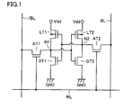
- an SRAM is a volatile semiconductor memory device, and a memory cell of the SRAM is a full CMOS (Complementary Metal Oxide Semiconductor) type memory cell.
- CMOS Complementary Metal Oxide Semiconductor
- the memory cell is disposed in each of intersections of complementary data lines (bit lines) BL and /BL and word lines WL.
- Complementary data lines (bit lines) BL and /BL and word lines WL are disposed in a matrix shape.
- the memory cell includes a flip-flop circuit provided with a pair of inverter circuits and two access transistors AT1 and AT2.
- Cross-coupled two storage nodes N1 and N2 are formed to obtain a bistable state of (High, Low) or (Low, High) by the flip-flop circuit.
- the memory cell continuously retains the bistable state as long as a predetermined power supply voltage is applied to the memory cell.
- Each of access transistors AT1 and AT2 includes an n-channel MOS transistor (hereinafter referred to as nMOS transistor).
- nMOS transistor n-channel MOS transistor
- One of a source and a drain of access transistor AT1 is electrically connected to storage node N1, and the other of the source and the drain is electrically connected to bit line /BL.
- One of the source and the drain of access transistor AT2 is electrically connected to storage node N2, and the other of the source and the drain is electrically connected to bit line BL.
- Each gate of access transistors AT1 and AT2 is electrically connected to word line WL. A conduction state and a non-conduction state of access transistor AT1 and AT2 are controlled through word line WL.
- the inverter circuit includes one driver transistor DT1 (or DT2) and one load transistor LT 1 (or LT2).
- Each of the pair of driver transistors DT1 and DT2 is formed by the nMOS transistor.
- Each source of driver transistors DT1 and DT2 is electrically connected to GND (ground potential).
- the drain of driver transistor DT1 is electrically connected to storage node N1, and the drain of driver transistor DT2 is electrically connected to storage node N2.
- the gate of driver transistor DT1 is electrically connected to storage node N2, and the gate of driver transistor DT2 is electrically connected to storage node N1.
- Each of the pair of load transistors LT1 and LT2 is formed by a p-channel MOS transistor (hereinafter referred to as pMOS transistor).
- pMOS transistor p-channel MOS transistor
- Each source of load transistors LT 1 and LT2 is electrically connected to a Vdd power supply voltage.
- the drain of load transistor LT1 is electrically connected to storage node N1, and the drain of load transistor LT2 is electrically connected to storage node N2.
- the gate of load transistor LT1 is electrically connected to storage node N2, and the gate of load transistor LT2 is electrically connected to storage node N1.
- word line WL is selected to put access transistors AT1 and AT2 in the conduction state, and a voltage is forcedly applied to bit line pair BL and /BL according to a desired logical value, thereby setting the flip-flop circuit at one of the bistable states.
- access transistors AT1 and AT2 are put in the conduction state, and potentials at storage nodes N1 and N2 are transferred to bit lines BL and /BL.
- a gate electrode layer of load transistor LT1 and a drain region of load transistor LT2 are electrically connected to each other by a shared contact; and a gate electrode layer of load transistor LT2 and a drain region of load transistor LT1 are electrically connected to each other by a shared contact.
- a trench isolation structure including STI Silicon Trench Isolation
- the trench isolation structure includes a trench isolation groove TR and a filling material TI.
- Trench isolation groove TR is formed in the main surface of semiconductor substrate SB, and groove TR is filled with filling material TI made of a silicon oxide.
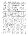
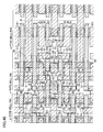
- the plural SRAM memory cells are formed in the main surface of semiconductor substrate SB isolated by the trench isolation structure. Pair of driver transistors DT1 and DT2, pair of access transistors AT1 and AT2, and pair of load transistors LT1 and LT2 are formed in one SRAM memory cell region MC (region surrounded by a broken line of Fig. 2 ).
- Each of pair of driver transistors DT1 and DT2 and each of pair of access transistors AT1 and AT2 are formed by the nMOS transistor, and driver transistors DT1 and DT2 and access transistors AT1 and AT2 are formed in p-type well regions PW1 and PW2 of the main surface of semiconductor substrate SB.
- Each of pair of load transistors LT1 and LT2 is formed by the pMOS transistor, and the load transistors LT1 and LT2 are formed in an n-type well region NW of the main surface of semiconductor substrate SB.
- Driver transistor DT1 includes a gate electrode layer GE1 and a pair of n-type impurity regions NIR and NIR which constitutes a pair of source/drain regions.
- N-type impurity regions NIR and NIR are formed with a spacing in the main surface of semiconductor substrate SB in p-type well region PW1.
- Gate electrode layer GE1 is formed on a channel formation region with a gate insulator (not shown) interposed therebetween, and the channel formation region is sandwiched between pair of n-type impurity regions NIR and NIR.
- Driver transistor DT2 includes a gate electrode layer GE2 and pair of n-type impurity regions NIR and NIR which constitutes pair of source/drain regions.
- N-type impurity regions NIR and NIR are formed with a spacing in the main surface of semiconductor substrate SB in p-type well region PW2.
- Gate electrode layer GE2 is formed on the channel formation region with a gate insulator (not shown) interposed therebetween, and the channel formation region is sandwiched between pair of n-type impurity regions NIR and NIR.
- Access transistor AT1 includes a gate electrode layer GE3 and pair of n-type impurity regions NIR and NIR which constitutes pair of source/drain regions.
- N-type impurity regions NIR and NIR are formed with a spacing in the main surface of semiconductor substrate SB in p-type well region PW1.
- Gate electrode layer GE3 is formed on the channel formation region with a gate insulator (not shown) interposed therebetween, and the channel formation region is sandwiched between pair of n-type impurity regions NIR and NIR.
- Access transistor AT2 includes a gate electrode layer GE4 and pair of n-type impurity regions NIR and NIR which constitutes pair of source/drain regions.
- N-type impurity regions NIR and NIR are formed with a spacing in the main surface of semiconductor substrate SB in p-type well region PW2.
- Gate electrode layer GE4 is formed on the channel formation region with a gate insulator (not shown) interposed therebetween, and the channel formation region is sandwiched between pair of n-type impurity regions NIR and NIR.
- Load transistor LT1 includes gate electrode layer GE1 and a pair of p-type impurity regions PIR and PIR which constitutes pair of source/drain regions.
- P-type impurity regions PIR and PIR are formed with a spacing in the main surface of semiconductor substrate SB in n-type well region NW.
- Gate electrode layer GE1 is formed on a channel formation region CHN1 with a gate insulator GI interposed therebetween, and channel formation region CHN1 is sandwiched between pair of p-type impurity regions PIR and PIR.
- Load transistor LT2 includes gate electrode layer GE2 and pair of p-type impurity regions PIR and PIR which constitutes pair of source/drain regions.
- P-type impurity regions PIR and PIR are formed with a spacing in the main surface of semiconductor substrate SB in n-type well region NW.
- Gate electrode layer GE2 is formed on a channel formation region CHN2 with gate insulator GI interposed therebetween, and channel formation region CHN2 is sandwiched between pair of p-type impurity regions PIR and PIR.
- the drain region of driver transistor DT1 and one of pair of source/drain regions of access transistor AT1 are formed by identical n-type impurity region NIR.
- the drain region of driver transistor DT2 and one of pair of source/drain regions of access transistor AT2 are formed by identical n-type impurity region NIR.
- Gate electrode layer GE1 of driver transistor DT1 and gate electrode layer GE1 of load transistor LT1 are formed by an identical conductive layer.
- Gate electrode layer GE2 of driver transistor DT2 and gate electrode layer GE2 of load transistor LT2 are formed by an identical conductive layer.
- a silicide layer SCL is formed so as to contact the gate electrode layer and the source/drain region of each of transistors DT1, DT2, AT1, AT2, LT1, and LT2.
- a liner nitride film LN and an inter-layer insulator IT1 are sequentially laminated on semiconductor substrate SB so as to cover the gate electrode layer and the source/drain region of each of transistors DT1, DT2, AT1, AT2, LT1, and LT2.
- inter-layer insulator III is made of a silicon oxide.
- Plural contact holes CH1 to CH8 and plural shared contact holes SC1 and SC2 are made in liner nitride film LN and inter-layer insulator II1.
- contact holes CH1 and CH2 that reach each source region of driver transistors DT1 and DT2 are made in liner nitride film LN and inter-layer insulator II1.
- Contact holes CH3 and CH4 that reach one (each drain region of driver transistors DT1 and DT2) of pair of source/drain regions of access transistors AT1 and AT2 are made in liner nitride film LN and inter-layer insulator II1.
- Contact holes CH5 and CH6 that reach the other of pair of source/drain regions of access transistors AT1 and AT2 are made in liner nitride film LN and inter-layer insulator II1.
- Contact holes CH7 and CH8 that reach each source region of load transistors LT1 and LT2 are made in liner nitride film LN and inter-layer insulator II1.
- Shared contact hole SC1 that reaches both gate electrode layer GE1 of load transistor LT1 and the drain region of load transistor LT2 is made in liner nitride film LN and inter-layer insulator II1.
- Shared contact hole SC2 that reaches both gate electrode layer GE2 of load transistor LT2 and the drain region of load transistor LT1 is made in liner nitride film LN and inter-layer insulator III.
- each inside of plural contact holes CH11 to CH18 and shared contact holes SC1 and SC2 is filled with a conductive layer PL1 ( Fig. 5 ).
- An insulator BL1 and an inter-layer insulator II2 are sequentially laminated on inter-layer insulator II1.
- insulator BL1 is made of a silicon nitride, a silicon carbide, a silicon oxy-carbide, or a silicon carbonitride.
- inter-layer insulator II2 is made of a silicon oxide.
- Plural through-holes are made in insulator BL1 and inter-layer insulator II2, and each of the plural through-holes is filled with each of plural conductive layers (first metal layer) CL1.
- a conductive layer pattern is formed by plural conductive layers CL1.
- conductive layer PL1 in shared contact hole SC1 and conductive layer PL1 in contact hole CH4 are electrically connected by conductive layer CL1. Therefore, gate electrode layer GE1 of load transistor LT1, the drain region of load transistor LT2, the drain region of driver transistor DT2, and one of the pair of source/drain regions of access transistor AT2 are electrically connected to one another.
- Conductive layer PL1 in shared contact hole SC2 and conductive layer PL1 in contact hole CH3 are electrically connected by conductive layer CL1. Therefore, gate electrode layer GE2 of load transistor LT2, the drain region of load transistor LT1, the drain region of driver transistor DT1, and one of the pair of source/drain regions of access transistor AT1 are electrically connected to one another.
- Conductive layer PL1 in each of contact holes CH1, CH2, and CH5 to CH8 is individually electrically connected to conductive layer CL1.
- an insulator BL2 and an inter-layer insulator II3 are sequentially laminated on inter-layer insulator II2.
- insulator BL2 is made of a silicon nitride, a silicon carbide, a silicon oxy-carbide, or a silicon carbonitride.
- inter-layer insulator II3 is made of a silicon oxide.
- Plural via holes VH11 to VH18 are made in insulator BL2 and inter-layer insulator II3, and a conductive layer embedding trench is made in a surface of inter-layer insulator II3 so as to communicate with each of plural via holes VH11 to VH18.
- a conductive layer PL2 is embedded in each of plural via holes VH11 to VH18.
- Each of plural conductive layers (second metal layer) CL2 is embedded in each of plural conductive layer embedding trenches.
- a conductive layer pattern is formed by plural conductive layers CL2.
- conductive layer CL2 electrically connected to the other of the pair of source/drain regions of access transistor AT1 through via hole VH13 and contact hole CH5 acts as bit line /BL.
- Conductive layer CL2 electrically connected to the other of the pair of source/drain regions of access transistor AT2 through via hole VH14 and contact hole CH6 acts as bit line BL.
- Conductive layer CL2 that is electrically connected to the source region of load transistor LT1 through via hole VH15 and contact hole CH7 and electrically connected to the source region of load transistor LT2 through via hole VH16 and contact hole CH8 acts as power supply line Vdd.
- Bit lines BL and /BL and power supply line Vdd are extended in parallel to a lengthwise direction of the drawings.
- Conductive layer PL2 in each of via holes VH11, VH12, VH17, and VH18 is individually electrically connected to conductive layer CL2.
- an insulator BL3 and an inter-layer insulator II4 are sequentially laminated on inter-layer insulator II3.
- insulator BL3 is made of a silicon nitride, a silicon carbide, a silicon oxy-carbide, or a silicon carbonitride.
- inter-layer insulator II4 is made of a silicon oxide.
- Plural via holes VH21 to VH24 are made in insulator BL3 and inter-layer insulator II4, and a conductive layer embedding trench is made in a surface of inter-layer insulator II4 so as to communicate with each of plural via holes VH21 to VH24.
- a conductive layer (not shown) is embedded in each of plural via holes VH21 to VH24.
- Each of plural conductive layers (third metal layer) CL3 is embedded in each of plural conductive layer embedding trenches.
- a conductive layer pattern is formed by plural conductive layers CL3.
- conductive layer CL3 electrically connected to the source region of driver transistor DT1 through via hole VH21, via hole VH11, and contact hole CH1 acts as a GND line.
- Conductive layer CL3 electrically connected to the source region of driver transistor DT2 through via hole VH22, via hole VH12, and contact hole CH2 acts as the GND line.
- Conductive layer CL3 that is electrically connected to gate electrode layer GE3 of access transistor AT1 through via hole VH23, via hole VH17, and contact hole CH9 and electrically connected to gate electrode layer GE3 of access transistor AT2 through via hole VH24, via hole VH18, and contact hole CH10 acts as word line WL.
- the GND line and word line WL are extended in parallel to a crosswise direction of the drawings.
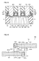
- shared contact hole SC1 reaches both gate electrode layer GE1 of load transistor LT1 and drain region (p-type impurity region) PIR of load transistor LT2.
- shared contact hole SC2 reaches both gate electrode layer GE2 of load transistor LT2 and drain region (p-type impurity region) PIR of load transistor LT 1.
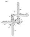
- Gate electrode layer GE1 includes sidewalls E1 and E2 and sidewalls E3 and E4.
- gate electrode layer GE1 includes sidewalls E1 and E2, and sidewalls E3 and E4.
- Sidewall E1 and sidewall E3 are located opposite to each other
- sidewall E2 and sidewall E4 are located opposite to each other.
- sidewall E2 in a portion that shared contact hole SC1 of gate electrode layer GE1 reaches is shifted toward sides of sidewalls E3 and E4 from a virtual extended line E1a of sidewall E1 in a portion located on channel formation region CHN1 of load transistor LT1 of gate electrode layer GE1.
- a center line (line C2-C2) of a line width D 1 in the portion that shared contact hole SC 1 of gate electrode layer GE 1 reaches is shifted toward the side of sidewall E4 from a center line (line C1-C1) of a line width D2 in the portion located on channel formation region CHN1 of gate electrode layer GE1. Therefore, line width D1 is shorter than line width D2.
- Line width D 1 and line width D2 are defined by sidewall E1, sidewall E3, and a line width in a perpendicular direction.
- the position shift of sidewall E2 with respect to virtual extended line E1a of sidewall E 1 is generated by providing a notch in the portion that shared contact hole SC1 of gate electrode layer GE1 reaches. That is, in the planar view, the portion that shared contact hole SC1 of gate electrode layer GE1 reaches has the notch such that sidewall E2 is retreated toward the side of sidewall E3 with respect to virtual extended line E1a of sidewall E1.
- Sidewall E2 is substantially parallel to sidewall E1.
- Sidewall E4 in the portion that shared contact hole SC1 of gate electrode layer GE1 reaches and sidewall E3 in the portion located on channel formation region CHN1 of gate electrode layer GE1 are substantially located on the same straight line.
- the shortest distance between an end of drain region (p-type impurity region) PIR of load transistor LT2 and sidewall E2 is not lower than 5 nm.
- Gate electrode layer GE2 has a configuration similar to that of gate electrode layer GE 1.
- p-type well regions PW1 and PW2 and n-type well region NW are formed in semiconductor substrate SB.
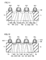
- Trench isolation groove TR is formed in the main surface of semiconductor substrate SB, and groove TR is filled with filling material Tr made of the silicon oxide, thereby obtaining the trench isolation structure formed by STI.
- a gate insulator GI and a gate electrode conductive layer GE are formed on the main surface of semiconductor substrate SB.
- a positive photoresist PR is applied onto gate electrode conductive layer GE.
- Photomask PM includes a substrate TS that transmits exposure light and light shielding pattern (for example, chromium film) LS that blocks the transmission of the exposure light. After the exposure, photoresist PR is developed.
- light shielding pattern for example, chromium film
- the region of photoresist PR irradiated with the exposure light is removed to perform the patterning of photoresist PR by the development.
- Etching is performed to gate electrode conductive layer GE with the pattern of photoresist PR as a mask. Therefore, the patterning of the gate electrode conductive layer is performed to form gate electrode layers GE1 to GE4. Then the pattern of photoresist PR is removed by ashing.
- an impurity is ion-implanted with gate electrode layers GE1 to GE4 as the mask, thereby forming a low-concentration region of the source/drain region in the main surface of semiconductor substrate SB.
- an n-type impurity and a p-type impurity are separately implanted to form an n-type low-concentration region and a p-type low-concentration region PIRL.
- a sidewall spacer insulator is formed such that gate electrode layers GE1 to GE4 are covered therewith.
- the sidewall spacer insulator is made of only a silicon oxide, or a silicon nitride is formed after the silicon oxide is formed. Then whole surface etch back is performed until the main surface of semiconductor substrate SB is exposed, whereby a sidewall spacer SW is formed while the sidewall spacer insulator remains in each sidewall of gate electrode layers GE1 to GE4.
- the impurity is ion-implanted with sidewall spacer SW and gate electrode layers GE1 to GE4 as the mask, thereby forming a high-concentration region of the source/drain region in the main surface of semiconductor substrate SB.
- the n-type impurity and the p-type impurity are separately implanted to form an n-type high-concentration region and a p-type high-concentration region PIRH.
- n-type source/drain region NIR having an LDD (Lightly Doped Drain) structure is formed by n-type low-concentration region and high-concentration region.
- p-type source/drain region PIR having the LDD structure is formed by p-type low-concentration region PIRL and p-type high-concentration region PIRH.
- a refractory metal layer is formed over the main surface of semiconductor substrate SB, and a heat treatment is performed to form a silicide layer SCL on gate electrode layers GE1 to GE4 and the main surface of semiconductor substrate SB. Then a portion that does not become the silicide is removed in the refractory metal layer.
- the refractory metal material can be selected from Ni, Co, Pt, Pd, Hf, V, Er, Ir, and Yb or a combination of at least two elements thereof.
- liner nitride film LN and inter-layer insulator II1 made of the silicon oxide are sequentially laminated on the main surface of semiconductor substrate SB such that gate electrode layers GE1 to GE4 and sidewall spacer SW are covered therewith.
- shared contact holes SC1 and SC2 and contact holes CH1 to CH10 are made in liner nitride film LN and inter-layer insulator II1 by a photoengraving process and the etching technique.
- shared contact hole SC1 is made so as to reach both gate electrode layer GE1 of load transistor LT1 and drain region PIR of load transistor LT2 (such that both the surface are exposed).
- shared contact hole SC2 is made so as to reach both gate electrode layer GE2 of load transistor LT2 and drain region PIR of load transistor LT1 (such that both the surface are exposed).
- a conductive layer made of tungsten (W) is formed on inter-layer insulator II1 so as to embed shared contact holes SC1 and SC2 and contact holes CH1 to CH10 by a CVD (Chemical Vapor Deposition) method or the like. Then the etch back is performed to the conductive layer until the surface of inter-layer insulator II1 is exposed, thereby forming conductive layer PL1 as a contact plug layer that embeds shared contact holes SC1 and SC2 and contact holes CH1 to CH10.
- CVD Chemical Vapor Deposition
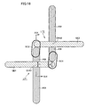
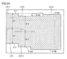
- a light shielding pattern LS is formed such that light shielding portions LS 1 and LS2 are located at a position corresponding to the gate electrode pattern.
- dimensions of the light shielding portion are set slightly larger than design values of the gate electrode layer. Therefore, dimensions of light shielding portion LS1 and LS2 of light shielding pattern LS are set larger than design values GE1D and GE2D of the gate electrode layer.
- light shielding portion LS1 includes a first pattern portion LS1a, a second pattern portion LS1b, and third pattern portion LS1c.
- First pattern portion LS1a corresponds to the portion of gate electrode layer GE1 formed on channel formation region CHN1 of load transistor LT1.
- Third pattern portion LS1c corresponds to the portion of the end on the side of shared contact hole SC1 of gate electrode layer GE1.
- Second pattern portion LS1b corresponds to the portion of gate electrode layer GE1 sandwiched between first pattern portion LS1a and third pattern portion LS1c, and second pattern portion LS1b corresponds to the portion in which the notch of gate electrode layer GE1 is formed.
- light shielding portion LS 1 includes sidewalls E11, E12A, and E12B and sidewalls E13, E14A, and E14B.
- sidewall E11 and sidewall E13 are located opposite to each other
- sidewall E12A and sidewall E14A are located opposite to each other
- sidewall E12B and sidewall E14B are located opposite to each other.
- sidewall E12A of second pattern portion LS1b is shifted toward the sides of sidewalls E13, E14A, and E14B of light shielding portion LS1 from a virtual extended line E11a of sidewall E11 of first pattern portion LS1a.
- a center line (line C12-C12) of a line width (2 ⁇ W12) of second pattern portion LS1b is shifted toward the sides of sidewalls E 13, E14A, and E 14B from a center line (line C11-C11) of a line width (2 ⁇ W11) of first pattern portion LS1a.
- Sidewall E12A is located on the sides of sidewalls E13, E14A, and E14B from sidewall E12B of third pattern portion LS1c.
- sidewall E2 of gate electrode layer GE1 is located on the side of sidewall E3 from virtual extended line E1a of sidewall E1. Therefore, the generation of the opening defect can be suppressed in forming shared contact hole SC1. The reason why the generation of the opening defect is suppressed will be described below.
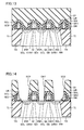
- FIG. 19 shows a schematic section taken on a line XIX-XIX of Fig. 18 in the middle of making the shared contact hole.
- the shared contact hole has a tapered shape in section in which an opening diameter is decreased at a deeper position from the opening end. Therefore, when shared contact hole SC2 pierces through inter-layer insulator II1 to reach liner nitride film LN, an etching area of liner nitride film LN exposed at the bottom of shared contact hole SC2 is also reduced.
- the projection of sidewall spacer SW located in the sidewall of gate electrode layer GE1 exists in the etching for making shared contact hole SC2, thereby decreasing a distance W1 between a lower end of liner nitride film LN along sidewall spacer SW and a lower end of an edge portion in a long-side direction of shared contact hole SC2.
- Distance W1 is further decreased when the position at which shared contact hole SC2 is made is shifted to a position shown by a solid line from a position shown by a dotted line in Fig. 19 due to a mask alignment error.
- a configuration of a second embodiment differs from the configuration of the first embodiment in that sidewall E2 is intersected with sidewall E1 while inclined relative to sidewall E1. Specifically, sidewall E2 is inclined so as to be retreated toward the side of sidewall E4 with respect to virtual extended line E1a of sidewall E1 as sidewall E2 is away from channel formation region CHN1, and sidewall E2 is intersected with virtual extended line E1a of sidewall E1 at an angle ⁇ 1.
- the center line (line C2-C2) of line width D1 in the portion that shared contact hole SC1 of gate electrode layer GE1 reaches is shifted toward the side of sidewall E4 with respect to the center line (line C1-C1) of line width D2 in the portion located on channel formation region CHN1 of gate electrode layer GE1.
- the center line (line C2-C2) of line width D1 is inclined relative to the center line (line C1-C1) of line width D2.
- Line width D1 and line width D2 are defined by sidewall E1, sidewall E3, and the line width in the perpendicular direction.
- the position shift of sidewall E2 with respect to virtual extended line E 1 a of sidewall E1 is generated by providing a notch in the portion that shared contact hole SC1 of gate electrode layer GE1 reaches. That is, in the planar view, the portion that shared contact hole SC1 of gate electrode layer GE1 reaches has the notch such that sidewall E2 is retreated and inclined toward the side of sidewall E3 with respect to virtual extended line E1a of sidewall E1.
- shortest distance L between sidewall E2 and the end of drain region (p-type impurity region) PIR of load transistor LT2 is not lower than 5 nm.
- Gate electrode layer GE2 has a configuration similar to that of gate electrode layer GE1.
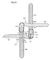
- light shielding portion LS1 of the photomask of the second embodiment has sidewalls E11, E12A, and E12B and sidewalls E13, E14A, and E14B.
- sidewalls E11, E12A, and E12B and sidewalls E13, E14A, and E14B are located opposite to each other.
- sidewall E12A of second pattern portion LS1b is shifted toward the sides of sidewalls E13, E14A, and E14B from virtual extended line E11a of sidewall E11 of first pattern portion LS1a.
- the center line (line C12-C12) of the line width (2 ⁇ W12) of second pattern portion LS1b is shifted toward the sides of sidewalls E13, E14A, and E 14B with respect to the center line (line C11-C11) of the line width (2 ⁇ W11) of first pattern portion LS1a.
- Sidewall E12B of third pattern portion LS1c located on a leading end side of light shielding portion LS1 with respect to sidewall E12A is further retreated toward the sides of sidewalls E13, E14A, and E14B from sidewall E12A of second pattern portion LS1b.
- sidewall E4 in the portion that shared contact hole SC 1 (or SC2) of gate electrode layer GE 1 (or GE2) reaches and sidewall E3 in the portion located on channel formation region CHN1 (or CHN2) of gate electrode layer GE1 (or GE2) are located on the same straight line.
- the present invention can also be applied to the case in which sidewall E4 and sidewall E3 are located on different straight lines. Therefore, third and fourth embodiments will be described for the case in which sidewall E4 and sidewall E3 are located on different straight lines.
- a configuration of the third embodiment differs from the configuration of the first embodiment in that sidewall E4 is located on a straight line different from that of sidewall E3.
- sidewall E4 in the portion that shared contact hole SC1 of gate electrode layer GE1 reaches is substantially extended in parallel with sidewall E3 in the portion located on channel formation region CHN1 of gate electrode layer GE1, and sidewall E4 is shifted toward the opposite side to sidewall E2 with respect to sidewall E3.
- Line width D1 in the portion that shared contact hole SC1 of gate electrode layer GE1 reaches may be equal to or different from line width D2 in the portion located on channel formation region CHN1 of gate electrode layer GE1.
- Line width D1 and line width D2 are defined by sidewall E1, sidewall E3, and the line width in the perpendicular direction.
- Gate electrode layer GE2 has a configuration similar to that of gate electrode layer GE 1.
- light shielding portion LS 1 of the photomask of the third embodiment has sidewalls E11, E12A, and E12B and sidewalls E13, E14A, and E14B.
- sidewalls E11, E12A, and E12B and sidewalls E13, E14A, and E14B are located opposite to each other.
- sidewall E12A of second pattern portion LS1b is shifted toward the side of sidewall E13 of light shielding portion LS1 from virtual extended line E11a of sidewall E11 of first pattern portion LS1a.
- the center line (line C12-C12) of the line width (2 ⁇ W12) of second pattern portion LS1b is shifted toward the side of sidewall E13 with respect to the center line (line C11-C11) of the line width (2 ⁇ W11) of first pattern portion LS1a.
- Second pattern portion LS1b is retreated toward the sides of sidewalls E14A and E14B with respect to sidewall E12B of third pattern portion LS1c that is located on the leading end side of light shielding portion LS 1 with respect to the sidewall E12A.
- Sidewall E14A is shifted toward the opposite side to sidewall E12A with respect to sidewall E13.
- Sidewall E14B is shifted toward the opposite side to sidewalls E12A and E12B with respect to sidewall E14A.
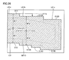
- a configuration of the fourth embodiment differs from the configuration of the second embodiment in that sidewall E4 is located on a straight line different from that of sidewall E3 and in that sidewall E2 and sidewall E4 are respectively inclined relative to sidewall E1 and sidewall E3.
- sidewall E2 in the portion that shared contact hole SC1 of gate electrode layer GE1 reaches is inclined so as to be retreated toward the side of sidewall E4 with respect to sidewall E1 in the portion located on channel formation region CHN1 of gate electrode layer GE1 as sidewall E2 is away from channel formation region CHN1.
- Line width D1 in the portion that shared contact hole SC1 of gate electrode layer GE1 reaches is inclined so as to be retreated toward the opposite side to sidewall E2 with respect to sidewall E3 in the portion located on channel formation region CHN1 of gate electrode layer GE1 as sidewall E4 is away from channel formation region CHN1.
- Line width D1 in the portion that shared contact hole SC1 of gate electrode layer GE1 reaches may be equal to or different from line width D2 in the portion located on channel formation region CHN1 of gate electrode layer GE1.
- Line width D2 is defined by sidewall E1, sidewall E3, and the line width in the perpendicular direction.
- Line width D1 is defined by sidewall E2, sidewall E4, and the line width in the perpendicular direction.
- Gate electrode layer GE2 has a configuration similar to that of gate electrode layer GE1.
- light shielding portion LS 1 of the photomask of the fourth embodiment has sidewalls E11, E12A, and E12B and sidewall E13 and E14A to E14C.
- sidewalls E11, E12A, and E12B and sidewalls E13 and E14A to E14C are located opposite to each other.
- sidewall E12A of second pattern portion LS1b is shifted toward the side of sidewall E13 of light shielding portion LS 1 from virtual extended line E11a of sidewall E11 of first pattern portion LS1a.
- the center line (line C12-C12) of the line width (2 ⁇ W12) of second pattern portion LS1b is shifted toward the side of sidewall E13 with respect to the center line (line C11-C11) of the line width (2 ⁇ W11) of first pattern portion LS1a.
- Sidewall E14A is shifted toward the opposite side to sidewall E12A with respect to sidewall E 13.
- Sidewall E 14C is shifted toward the opposite side to sidewalls E12A with respect to sidewall E14A.
- Sidewall E14B is shifted toward the opposite side to sidewall E12A with respect to sidewall E 14C.
- the shared contact hole reaches both the gate electrode layer of one of the load transistors and the drain region of the other load transistor.
- the shared contact hole may reach both a gate electrode layer of another transistor and another impurity region.
- SRAM is described as the device having shared contact hole by way of example.
- the present invention can be applied to other devices except for SRAM as long as the device has the shared contact hole.
- SRAM is formed by the MOS transistors.
- the present invention is not limited to the MOS transistor, but can be applied to insulated gate field effect transistors.
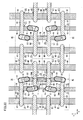
- a configuration of each memory cell MC shown in Fig. 27 is substantially identical to the configuration of the memory cell MC shown in Figs. 2 to 6 .
- memory cells MC that are adjacent to each other in an X-direction of Fig. 27 have planar layouts that are symmetrical in relation to a virtual cell boundary line.
- One of gate electrode layers GE3 and GE4 is shared by memory cells MC adjacent to each other in the X-direction. That is, gate electrode layer GE3 of one of memory cells MC adjacent to each other in the X-direction and gate electrode layer GE3 of the other memory cell MC constitute an integrated conductive layer, or gate electrode layer GE4 of one of memory cells MC adjacent to each other in the X-direction and gate electrode layer GE4 of the other memory cell MC constitute an integrated conductive layer.
- Memory cells MC that are adjacent to each other in a Y-direction of Fig. 27 have planar layouts that are symmetrical in relation to a virtual cell boundary line.
- each of source/drain regions NIR of access transistor AT 1, source regions PIR of load transistor LT2, and source regions NIR of driver transistor DT2 is formed by the single impurity region, or each of source/drain regions NIR of access transistor AT2, source regions PIR of load transistor LT1, and source regions NIR of driver transistor DT1 is formed by the single impurity region.
- sidewalls E3 and E4 of gate electrode layer GE2 are located opposite to each other in the planar view, or sidewalls E3 and E4 of gate electrode layer GE1 are located opposite to each other in the planar view.
- a spacing LE2a between sidewall E 1 of gate electrode layer GE2 of one of memory cells MC and sidewall E1 of gate electrode layer GE2 of the other memory cell MC is larger than a spacing LEI a between sidewall E2 of gate electrode layer GE2 of one of memory cells MC and sidewall E2 of gate electrode layer GE2 of the other memory cell MC.
- a spacing between sidewall E 1 of gate electrode layer GE 1 of one of memory cells MC and sidewall E 1 of gate electrode layer GE 1 of the other memory cell MC is larger than a spacing between sidewall E2 of gate electrode layer GE1 of one of memory cells MC and sidewall E2 of gate electrode layer GE1 of the other memory cell MC.
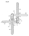
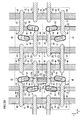
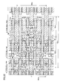
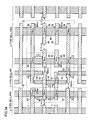
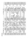
- the configuration of the SRAM memory cells arrayed in the 2 ⁇ 2 matrix can be applied to the configuration of the second embodiment as shown in Fig. 28 , applied to the configuration of the third embodiment as shown in Fig. 29 , and applied to the configuration of the fourth embodiment as shown in Fig. 30 .
- a spacing LE2b between sidewall E3 of gate electrode layer GE2 of one of memory cells MC and sidewall E3 of gate electrode layer GE2 of the other memory cell MC is larger than a spacing LE1b between sidewall E4 of gate electrode layer GE2 of one of memory cells MC and sidewall E4 of gate electrode layer GE2 of the other memory cell MC.
- a spacing between sidewall E3 of gate electrode layer GE1 of one of memory cells MC and sidewall E3 of gate electrode layer GE1 of the other memory cell MC is larger than a spacing between sidewall E4 of gate electrode layer GE1 of one of memory cells MC and sidewall E4 of gate electrode layer GE 1 of the other memory cell MC.
- the configurations of the first to fourth embodiments can also be applied to a CAM (Content Addressable Memory) memory cell whose storage unit has the configuration of the SRAM memory cell.
- CAM memory cell in which three-level data is stored that is, TCAM (Ternary CAM) will be described below by way of example.
- the TCAM cell includes a data storage unit MR and a search unit SR.
- Search candidate data is stored in data storage unit MR.
- Search unit SR compares the search candidate data and pieces of search data SL and /SL, and search unit SR drives a match line ML according to the comparison result.
- Data storage unit MR includes two memory cells (cell X1 and cell Y1). Each of cell X1 and cell Y1 has the configuration of the SRAM memory cell. Cell X1 and cell Y1 have the same structure, and cell X1 and cell Y1 have the same structure as the SRAM memory cell of Fig. 1 . Therefore, in Fig. 31 , the same component of cell X1 and cell Y1 as the SRAM memory cell of Fig. 1 is designated by the same numeral, and the description is not repeated.
- the three-level data can be stored in the TCAM cell by utilizing two memory cells X1 and Y1.
- Search unit SR includes MOS transistors TQ1 and TQ2 provided in relation to cell X1 and MOS transistors TQ3 and TQ4 provided in relation to cell Y1.
- MOS transistors TQ1 and TQ2 are connected in series between match line ML and a ground node.
- the gate of MOS transistor TQ1 is connected to a storage node N2 of cell X1.
- the gate of MOS transistor TQ2 is connected to a search candidate data bit line SL.
- MOS transistors TQ3 and TQ4 are connected in series between match line ML and the ground node.
- the gate of MOS transistor TQ3 is connected to a storage node N2 of cell Y1.
- the gate of MOS transistor TQ4 is connected to a search data inverted bit line /SL.
- TCAM cell realizes the three-level state as follows.
Landscapes
- Semiconductor Memories (AREA)
- Thin Film Transistor (AREA)
- Internal Circuitry In Semiconductor Integrated Circuit Devices (AREA)
Applications Claiming Priority (2)
| Application Number | Priority Date | Filing Date | Title |
|---|---|---|---|
| JP2007339965A JP5272203B2 (ja) | 2007-12-28 | 2007-12-28 | 半導体装置およびフォトマスク |
| JP2008257545A JP2010087420A (ja) | 2008-10-02 | 2008-10-02 | 半導体装置およびフォトマスク |
Publications (2)
| Publication Number | Publication Date |
|---|---|
| EP2075831A2 true EP2075831A2 (de) | 2009-07-01 |
| EP2075831A3 EP2075831A3 (de) | 2010-09-01 |
Family
ID=40430073
Family Applications (1)
| Application Number | Title | Priority Date | Filing Date |
|---|---|---|---|
| EP08254137A Withdrawn EP2075831A3 (de) | 2007-12-28 | 2008-12-23 | Halbleitervorrichtung mit geteiltem Kontaktloch für Gate-Elektrode und Drain-Gebiet |
Country Status (4)
| Country | Link |
|---|---|
| US (1) | US8120116B2 (de) |
| EP (1) | EP2075831A3 (de) |
| KR (1) | KR101548018B1 (de) |
| TW (1) | TWI433267B (de) |
Cited By (1)
| Publication number | Priority date | Publication date | Assignee | Title |
|---|---|---|---|---|
| GB2489682A (en) * | 2011-03-30 | 2012-10-10 | Pragmatic Printing Ltd | Thin film transistor and its method of manufacture |
Families Citing this family (10)
| Publication number | Priority date | Publication date | Assignee | Title |
|---|---|---|---|---|
| JP2010205908A (ja) * | 2009-03-03 | 2010-09-16 | Toshiba Corp | 半導体装置およびその製造方法 |
| JP2012156229A (ja) * | 2011-01-25 | 2012-08-16 | Renesas Electronics Corp | 半導体装置およびその製造方法 |
| CN104576536B (zh) * | 2013-10-10 | 2017-11-14 | 中芯国际集成电路制造(上海)有限公司 | 一种半导体器件及其制造方法和电子装置 |
| JP2016082107A (ja) | 2014-10-17 | 2016-05-16 | 株式会社東芝 | 記憶装置及びその製造方法 |
| JP2017108031A (ja) | 2015-12-11 | 2017-06-15 | ルネサスエレクトロニクス株式会社 | 半導体装置 |
| FR3069369B1 (fr) * | 2017-07-21 | 2019-11-01 | Stmicroelectronics (Rousset) Sas | Circuit integre comportant un contact partage masque |
| CN113299648B (zh) * | 2020-06-05 | 2024-12-24 | 台湾积体电路制造股份有限公司 | 半导体器件及其制造方法 |
| CN114284267A (zh) | 2020-11-13 | 2022-04-05 | 台湾积体电路制造股份有限公司 | 集成电路及其制造方法 |
| US12107132B2 (en) * | 2021-09-30 | 2024-10-01 | International Business Machines Corporation | Source/drain contact positioning under power rail |
| US12538790B2 (en) * | 2023-08-11 | 2026-01-27 | Nanya Technology Corporation | Electrical structure and method of manufacturing the same |
Citations (4)
| Publication number | Priority date | Publication date | Assignee | Title |
|---|---|---|---|---|
| JPH09321152A (ja) | 1996-05-31 | 1997-12-12 | Nec Corp | 半導体装置 |
| JP2004273642A (ja) | 2003-03-06 | 2004-09-30 | Matsushita Electric Ind Co Ltd | 半導体装置およびその製造方法 |
| JP2004273972A (ja) | 2003-03-12 | 2004-09-30 | Renesas Technology Corp | 半導体装置 |
| JP2004327796A (ja) | 2003-04-25 | 2004-11-18 | Toshiba Corp | 半導体装置 |
Family Cites Families (5)
| Publication number | Priority date | Publication date | Assignee | Title |
|---|---|---|---|---|
| US5675533A (en) | 1994-09-26 | 1997-10-07 | Texas Instruments Incorporated | Semiconductor device |
| JP4471504B2 (ja) * | 2001-01-16 | 2010-06-02 | 株式会社ルネサステクノロジ | 半導体記憶装置 |
| US7304874B2 (en) | 2005-03-08 | 2007-12-04 | Lsi Corporation | Compact ternary and binary CAM bitcell architecture with no enclosed diffusion areas |
| JP4768399B2 (ja) | 2005-10-31 | 2011-09-07 | 株式会社東芝 | 半導体装置 |
| JP5153136B2 (ja) | 2005-12-28 | 2013-02-27 | 株式会社半導体エネルギー研究所 | 半導体装置の製造方法 |
-
2008
- 2008-12-22 US US12/341,664 patent/US8120116B2/en active Active
- 2008-12-23 TW TW097150207A patent/TWI433267B/zh active
- 2008-12-23 EP EP08254137A patent/EP2075831A3/de not_active Withdrawn
- 2008-12-24 KR KR1020080133637A patent/KR101548018B1/ko active Active
Patent Citations (4)
| Publication number | Priority date | Publication date | Assignee | Title |
|---|---|---|---|---|
| JPH09321152A (ja) | 1996-05-31 | 1997-12-12 | Nec Corp | 半導体装置 |
| JP2004273642A (ja) | 2003-03-06 | 2004-09-30 | Matsushita Electric Ind Co Ltd | 半導体装置およびその製造方法 |
| JP2004273972A (ja) | 2003-03-12 | 2004-09-30 | Renesas Technology Corp | 半導体装置 |
| JP2004327796A (ja) | 2003-04-25 | 2004-11-18 | Toshiba Corp | 半導体装置 |
Cited By (5)
| Publication number | Priority date | Publication date | Assignee | Title |
|---|---|---|---|---|
| GB2489682A (en) * | 2011-03-30 | 2012-10-10 | Pragmatic Printing Ltd | Thin film transistor and its method of manufacture |
| GB2490752A (en) * | 2011-03-30 | 2012-11-14 | Pragmatic Printing Ltd | Thin film transistor and its method of manufacture |
| GB2490752B (en) * | 2011-03-30 | 2015-10-28 | Pragmatic Printing Ltd | Thin film transistor and its method of manufacture |
| GB2489682B (en) * | 2011-03-30 | 2015-11-04 | Pragmatic Printing Ltd | Electronic device and its method of manufacture |
| US9530649B2 (en) | 2011-03-30 | 2016-12-27 | Pragmatic Printing Ltd. | Semiconductor electronic devices and methods of manufacture thereof |
Also Published As
| Publication number | Publication date |
|---|---|
| TWI433267B (zh) | 2014-04-01 |
| KR101548018B1 (ko) | 2015-08-27 |
| US8120116B2 (en) | 2012-02-21 |
| KR20090073009A (ko) | 2009-07-02 |
| EP2075831A3 (de) | 2010-09-01 |
| TW200943482A (en) | 2009-10-16 |
| US20090166745A1 (en) | 2009-07-02 |
Similar Documents
| Publication | Publication Date | Title |
|---|---|---|
| EP2075831A2 (de) | Halbleitervorrichtung mit geteiltem Kontaktloch für Gate-Elektrode und Drain-Gebiet | |
| KR100746220B1 (ko) | 적층된 노드 콘택 구조체들과 적층된 박막 트랜지스터들을채택하는 반도체 집적회로들 및 그 제조방법들 | |
| US8004042B2 (en) | Static random access memory (SRAM) cell and method for forming same | |
| CN101471345B (zh) | 半导体装置和光掩膜 | |
| US7528046B2 (en) | Method for manufacturing semiconductor device | |
| US20120187504A1 (en) | Semiconductor Device Having Shared Contact Hole and a Manufacturing Method Thereof | |
| JP2005203780A (ja) | ノードコンタクト構造体、それを有する半導体素子、及びその配線構造体、並びにその製造方法 | |
| US20080203493A1 (en) | Semiconductor memory device and fabrication process thereof | |
| KR100749109B1 (ko) | 반도체 기억 장치 및 반도체 장치군 | |
| CN101266973B (zh) | 半导体器件及其制造工艺 | |
| KR100514173B1 (ko) | 반도체 장치의 게이트 형성 방법. | |
| US20090090973A1 (en) | Semiconductor device and method of manufacturing the same | |
| JP2010087420A (ja) | 半導体装置およびフォトマスク | |
| US20070181958A1 (en) | Semiconductor device and method of forming the same | |
| JP2008041895A (ja) | 半導体装置およびその製造方法 | |
| US7250661B2 (en) | Semiconductor memory device with plural source/drain regions | |
| US7825471B2 (en) | Semiconductor memory device including SRAM cell having well power potential supply region provided therein | |
| KR20100055731A (ko) | 레티클 및 반도체 소자의 형성 방법 | |
| KR20050024099A (ko) | 에스램 소자의 제조방법 및 그에 의해 제조된 에스램 소자 | |
| KR20090025084A (ko) | 스태틱 메모리 소자 및 그 제조 방법 | |
| JP2005347296A (ja) | 半導体装置および半導体装置の製造方法 | |
| JP2005347360A (ja) | 半導体装置及びその製造方法 | |
| US20070152279A1 (en) | Sram device | |
| US20090085124A1 (en) | Semiconductor storage device and manufacturing method of the same | |
| JP2009010274A (ja) | 半導体装置およびその製造方法 |
Legal Events
| Date | Code | Title | Description |
|---|---|---|---|
| PUAI | Public reference made under article 153(3) epc to a published international application that has entered the european phase |
Free format text: ORIGINAL CODE: 0009012 |
|
| AK | Designated contracting states |
Kind code of ref document: A2 Designated state(s): AT BE BG CH CY CZ DE DK EE ES FI FR GB GR HR HU IE IS IT LI LT LU LV MC MT NL NO PL PT RO SE SI SK TR |
|
| AX | Request for extension of the european patent |
Extension state: AL BA MK RS |
|
| PUAL | Search report despatched |
Free format text: ORIGINAL CODE: 0009013 |
|
| AK | Designated contracting states |
Kind code of ref document: A3 Designated state(s): AT BE BG CH CY CZ DE DK EE ES FI FR GB GR HR HU IE IS IT LI LT LU LV MC MT NL NO PL PT RO SE SI SK TR |
|
| AX | Request for extension of the european patent |
Extension state: AL BA MK RS |
|
| RIC1 | Information provided on ipc code assigned before grant |
Ipc: H01L 29/423 20060101ALI20100727BHEP Ipc: H01L 21/768 20060101ALI20100727BHEP Ipc: H01L 27/11 20060101ALI20100727BHEP Ipc: H01L 27/105 20060101ALI20100727BHEP Ipc: H01L 27/02 20060101ALI20100727BHEP Ipc: H01L 21/8244 20060101ALI20100727BHEP Ipc: H01L 21/8239 20060101AFI20090320BHEP |
|
| RAP1 | Party data changed (applicant data changed or rights of an application transferred) |
Owner name: RENESAS ELECTRONICS CORPORATION |
|
| 17P | Request for examination filed |
Effective date: 20101103 |
|
| 17Q | First examination report despatched |
Effective date: 20110217 |
|
| AKX | Designation fees paid |
Designated state(s): DE FR GB IT |
|
| STAA | Information on the status of an ep patent application or granted ep patent |
Free format text: STATUS: THE APPLICATION HAS BEEN WITHDRAWN |
|
| 18W | Application withdrawn |
Effective date: 20121227 |