EP2048786A2 - Datenprozessor, Festkörperabbildungsvorrichtung, Abbildungsvorrichtung und elektronisches Gerät - Google Patents
Datenprozessor, Festkörperabbildungsvorrichtung, Abbildungsvorrichtung und elektronisches Gerät Download PDFInfo
- Publication number
- EP2048786A2 EP2048786A2 EP08017815A EP08017815A EP2048786A2 EP 2048786 A2 EP2048786 A2 EP 2048786A2 EP 08017815 A EP08017815 A EP 08017815A EP 08017815 A EP08017815 A EP 08017815A EP 2048786 A2 EP2048786 A2 EP 2048786A2
- Authority
- EP
- European Patent Office
- Prior art keywords
- count
- signal
- counter
- count operation
- reference signal
- Prior art date
- Legal status (The legal status is an assumption and is not a legal conclusion. Google has not performed a legal analysis and makes no representation as to the accuracy of the status listed.)
- Granted
Links
Images










Classifications
-
- H—ELECTRICITY
- H03—ELECTRONIC CIRCUITRY
- H03K—PULSE TECHNIQUE
- H03K21/00—Details of pulse counters or frequency dividers
- H03K21/08—Output circuits
-
- H—ELECTRICITY
- H03—ELECTRONIC CIRCUITRY
- H03M—CODING; DECODING; CODE CONVERSION IN GENERAL
- H03M1/00—Analogue/digital conversion; Digital/analogue conversion
- H03M1/12—Analogue/digital converters
- H03M1/50—Analogue/digital converters with intermediate conversion to time interval
- H03M1/56—Input signal compared with linear ramp
-
- H—ELECTRICITY
- H04—ELECTRIC COMMUNICATION TECHNIQUE
- H04N—PICTORIAL COMMUNICATION, e.g. TELEVISION
- H04N25/00—Circuitry of solid-state image sensors [SSIS]; Control thereof
- H04N25/70—SSIS architectures; Circuits associated therewith
- H04N25/76—Addressed sensors, e.g. MOS or CMOS sensors
- H04N25/77—Pixel circuitry, e.g. memories, A/D converters, pixel amplifiers, shared circuits or shared components
-
- H—ELECTRICITY
- H04—ELECTRIC COMMUNICATION TECHNIQUE
- H04N—PICTORIAL COMMUNICATION, e.g. TELEVISION
- H04N25/00—Circuitry of solid-state image sensors [SSIS]; Control thereof
- H04N25/70—SSIS architectures; Circuits associated therewith
- H04N25/76—Addressed sensors, e.g. MOS or CMOS sensors
- H04N25/78—Readout circuits for addressed sensors, e.g. output amplifiers or A/D converters
-
- H—ELECTRICITY
- H03—ELECTRONIC CIRCUITRY
- H03M—CODING; DECODING; CODE CONVERSION IN GENERAL
- H03M1/00—Analogue/digital conversion; Digital/analogue conversion
- H03M1/10—Calibration or testing
- H03M1/1009—Calibration
- H03M1/1014—Calibration at one point of the transfer characteristic, i.e. by adjusting a single reference value, e.g. bias or gain error
- H03M1/1023—Offset correction
-
- H—ELECTRICITY
- H03—ELECTRONIC CIRCUITRY
- H03M—CODING; DECODING; CODE CONVERSION IN GENERAL
- H03M1/00—Analogue/digital conversion; Digital/analogue conversion
- H03M1/12—Analogue/digital converters
- H03M1/1205—Multiplexed conversion systems
- H03M1/123—Simultaneous, i.e. using one converter per channel but with common control or reference circuits for multiple converters
Definitions
- a count period (count operation period) in the AD conversion scheme called a reference signal comparison type is independently controlled on the basis of a predetermined criterion.
- “To independently control the count operation period” means that it is controlled whether the actual count operation (in other words, real number count operation) should be performed in the first half of the entire AD conversion period or the actual count operation (in other words, complement number count operation) should be performed in the second half.
- a typical example in which the CDS functional units or the analog-digital converters are disposed in parallel to the columns is a column type in which the CDS functional units or the analog-digital converters are disposed every vertical columns in a column area disposed on the output side of an imaging unit so as to sequentially read out signals to the output side.
- a type in which one CDS functional unit or analog-digital converter is assigned to neighboring plural (for example, two) vertical signal lines 19 (vertical columns) or a type in which one CDS functional unit or analog-digital converter is assigned to N vertical signal lines 19 (vertical columns) with an N interval (where N is a positive integer and N-1 lines are arranged in the interval) may be employed.
- a solid-state imaging device 1 includes a pixel array unit 10 which is called a pixel unit or an imaging unit and in which plural unit pixels 3 are arranged in rows and columns, a driving controller 7 disposed outside the pixel array unit 10, a reading current source unit 24 supplying the unit pixels 3 of the pixel array unit 10 with operation current (reading current) for reading a pixel signal, a column processor 26 having column AD circuits 25 disposed by vertical columns, and an output circuit (sense amplifier: S/A) 28.
- the functional units are disposed on a single semiconductor substrate.
- the unit pixel 3 generally includes a photo diode as a light-receiving element (charge generator) which is an example of a sensor and an intra-pixel amplifier (an example of a pixel signal generator) having a semiconductor element (for example, transistor) for amplification.
- a photo diode as a light-receiving element (charge generator) which is an example of a sensor and an intra-pixel amplifier (an example of a pixel signal generator) having a semiconductor element (for example, transistor) for amplification.
- the solid-state imaging device 1 can allow a pixel array unit 10 to cope with color imaging by employing a color separation filter. That is, one color filter of color separation filters having a combination of color filters of plural colors for taking a color image is provided on a light-receiving surface on which electromagnetic waves (light in this embodiment) from the charger generators (photo diodes) in the pixel array unit 10 are incident, for example, in a so-called Bayer arrangement, thereby coping with the color imaging.
- the driving controller 7 has a control circuit function of sequentially reading signals from the pixel array unit 10.
- the driving controller 7 includes a horizontal scanner (column scanning circuit) 12 controlling column addresses or column scanning, a vertical scanner (row scanning circuit) 14 controlling a row address or row scanning, and a communication timing controller 20 having a function of generating a built-in clock.
- the solid-state imaging device 1 may have a one chip structure in which the constituent elements are monolithically formed in a semiconductor area, or may have a module structure having an imaging function in which optical systems such as an imaging lens, an optical low-pass filter, and an infrared cut filter as well as the signal processors such as the pixel array unit 10, the driving controller 7, and the column processor 26 are collected and packaged.
- the pixel signals output from the unit pixels 3 are supplied to the column AD circuits 25 of the column processor 26 through the vertical signal lines 19 by vertical columns.
- the switch 258 When it is supplied with the memory transmission instructing pulse CN8 on the basis of a load function, the switch 258 transmits data of the AD converter 25b in the corresponding column to the data storage and transmission output unit 256.
- the data storage and transmission output unit 256 stores the transmitted data.
- the AD conversion data stored in the AD converter 25b can be transmitted to the data storage and transmission output unit 256. Accordingly, it is possible to independently control the AD conversion process of the AD converter 25b and the reading operation of the AD conversion result to the horizontal signal line 18 and thus to embody a pipeline operation of performing the AD conversion process and the signal reading operation to the outside in parallel.
- the AD converter 25b completes the AD conversion by latching (storing) the AD conversion result of the pixel data therein. Thereafter, the data is transmitted to the data storage and transmission output unit 256 and stored therein at a predetermined timing. Thereafter, the column AD circuit 25 sequentially outputs the pixel data stored in the data storage and transmission output units 256 from the chip having the column processor 26 and the pixel array unit 10 through an output terminal 5c by the shift operation synchronized with the control pulse input from the horizontal scanner 12 through the control line 12c at a predetermined timing.
- the AD converter 25b includes a voltage comparator 252 comparing the reference signal SLP_ADC generated by the DA conversion circuit 27a of the reference signal generator 27 with an analog pixel signal acquired through the vertical signal lines 19 (H1, H2, ..., Hh) from the unit pixels 3 in the unit of row control lines 15 (V1, V2, V3, ..., Vv) and a counter unit 254 as an example of a counter counting a period of time until the voltage comparator 252 completes the comparison process or a period of time in a predetermined time after the completion and storing the result, and has an n-bit AD conversion function.
- Various usages can be considered for the count period control signal SEL. For example, a usage of uniformly controlling the effective count operation periods of the counter units 254 of the entire columns, a usage of grouping the vertical columns into several groups (generally two groups) and controlling the effective count operation periods by the groups, or a usage of controlling the effective count operation period depending on the level of the pixel signal voltage Vx can be considered.
- the voltage comparator 252 disposed every column is supplied with the reference signal SLP_ADC from the DA conversion circuit 27a, and the pixel signal voltage Vx to be processed by the voltage comparators 252 is subjected to the comparison process using the common reference signal SLP_ADC.
- the counter unit 254 performs a count process using the output of the count phase adjuster 260 as the count enable signal EN on the basis of the count clock CK_CNT when the count enable signal EN is at the H level, and stores the count result at the time of end of the count process.
- the count clock CK_CNT is input to the clock terminal CK of the counter unit 254 from the communication timing controller 20 in common to the clock terminals CK of other counter units 254.
- the counter unit 254 can be embodied by changing the wiring type of the data storage including latches to a synchronous counter type, and performs an internal count process with the input of one count clock CK_CNT.
- the maximum count number Dsm' of the comparison process of the D-phase process is set to a value obtained by adding the maximum count number Drm of the P-phase process to the maximum value of the AD conversion result of the signal component Vsig, that is, the maximum count number Dsm corresponding to the maximum signal component Vsig.
- the maximum count number Dsm is, for example, in the range of the 10-bit count number (1024 clocks) to the 12-bit count number (4096 clocks).
- the maximum period of the comparison process on the reset level Srst is made to be shorter than the maximum period of the comparison process on the signal level Ssig. By not setting both periods to be equal but setting both periods in this way, the total AD conversion period of two conversion processes is shortened.
- the down-count operation and the up-count operation are switched in two count processes for acquiring the digital data Dsig of the pixel signal component Vsig. Accordingly, the updown counter switching the down-count operation and the up-count operation is preferably used as the counter unit 254.
- the inverted bit data can be output from the data storage and transmission output unit 256 or the bit data can be inverted by the digital calculator 29.
- the digital calculator 29 can add "1" thereto to obtain the accurate data.
- the digital calculator 29 may be acquired.
- Dsig can be obtained as a negative value by combining the negative counting characteristic of the complement number count operation and the positive counting characteristic of the up count process. "Dsm-Dsig" indicates that.
- the P-phase process is performed in the down count mode and the D-phase process is performed in the up count mode has been described.
- the P-phase process may be performed in the up count mode and the D-phase process may be performed in the down count mode.
- the data stored in the counter unit 254 after the D-phase process is "Dini-Dsm+Dsig" and the AD conversion data Dsig of the signal component Vsig is a positive number.
- the initial value Dini in the P-phase process is set to Dsm, or the digital calculator 29 can add Dsm to "Dsig-Dsm" when the initial value Dini is "0.”
- the complement number count operation is performed in both the first count process and the second count process on one pixel, the negative count process is performed in one process, and the positive count process is performed in the other process.
- the complement number count operation can be considered substantially as the negative count process.
- the process result thereof can be considered as an addition factor.
- the complement number count operation is performed in the positive direction, the process result thereof can be considered as the subtraction factor.
- the coefficient can be properly set.
- the first configuration example shown in Fig. 2A or the second configuration example shown in Fig. 2B can be employed as the circuit configuration.
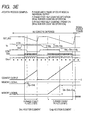
- the real number count process as the first-half count operation and the complement number count process as the second-half count operation are combined using as a reference the time point when the comparison output COMP is inverted.
- the count number Drst_cnt in the AD conversion process on the first reset level Srst is the digital value Drst of the reset level Srst. Accordingly, in consideration of the down count mode, the count value D1 stored in the counter unit 254 after the first AD conversion process is expressed by Expression (4) shown in the drawing.
- the count value D2 stored in the counter unit 254 after the second AD conversion process is expressed by Expression (5-1) shown in the drawing.
- the initial value Dini is set to the maximum count number Dsm', but may be set to "0."
- the maximum count number Dsm' is a constant and can be externally adjusted by the communication timing controller 20. The value can be determined depending on the maximum AD conversion period of the signal level Ssig.
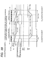
- the column AD circuit 25_e of the even columns performs the count operation in the first half of the maximum process period (until the comparison output COMP_e is inverted) during both the P-phase process period and the D-phase process period.
- the counter units 254_o start the count operation in the up count mode.
- the count initial value is set to the maximum gray scale value (maximum value) of the AD conversion, for example, "4096" when the signal component Vsig is converted into digital data by 12 bits.
- This value is the maximum count number Dsm corresponding to the maximum signal component Vsig_o of the D-phase process.
- the column AD circuit 25_o of the odd columns performs the count operation in the second half (after the comparison output COMP_o is inverted) of the maximum process time during both the P-phase process period (reset counter period) and the D-phase process period (data counter period).
- the count activation periods are complementary with each other to reduce the influence of the input amplitude on the power consumption, for example, to equalize the power consumption with respect to the input amplitude.
- the counter units 254 corresponding to a half of the entire columns operate during the entire process period, regardless of the amplitude of the pixel signal voltage Vx, thereby reducing the peak source current to about 1/2.
- the total power consumption is not equal to the power consumption at the time of processing the pixel signal voltage Vs of the middle level.
- the count period is elongated in both the even columns and the odd columns and the total power consumption is greater than the power consumption at the time of processing the pixel signal voltage Vx of the middle level.
- the count operation is performed on the reset level Srst_e in the first half (until the comparison output COMP_o is inverted) of the maximum process period and the count operation is performed on the reset level Srst_o (the value of which is equal to the reset level Srst_e) in the second half (after the comparison output COMP_o is inverted) of the maximum process period. Accordingly, the counter units 254 of the even columns and the odd columns operate with the complementary relation and thus do not operate at the same time.
- the voltage comparators 252 compare the reference signal SLP_ADC with the pixel signal voltage Vx_o.
- the comparison output COMP_o of the voltage comparators 252 is inverted and then is logically inverted by the inverter circuit 264, and is transmitted as the comparison output xCOMP_o to the counter units 254.
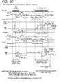
- Figs. 5A to 5C are diagrams illustrating a structure for independently controlling the counter activation period of the counter units 254 according to a second example of the first embodiment.
- Fig. 5A is a block diagram illustrating a circuit configuration for putting the first embodiment (second example) into practice.
- Fig. 5B is a timing diagram illustrating a basic operation of the first embodiment (second example).
- Fig. 5C is a timing diagram illustrating a specific example of the first embodiment (second example).
- the first embodiment (second example) provides a structure for independently controlling the counters disposed to exclusively perform the first-half count operation and the second-half count operation by using the first example of the relation between the "predetermined criterion" and the "independent control" corresponding to the predetermined criterion. Accordingly, a first counter performing the first-half count operation and a second counter performing the second-half count operation are individually provided and the processing signal is distributed thereto.
- the basic operation of the first embodiment is shown in the timing diagram of Fig. 5B .
- the operation of the column AD circuit 25_e of the even columns is equal to the operation of the first embodiment (first example) shown in Fig. 4B . Accordingly, the description thereof is omitted.
- the counter units 254 perform the reading and AD conversion process on the first pixel signal voltage Vx_o in the down count mode as follows. After the reset level Srst_o is stabilized, the voltage comparator 252 compares the reference signal SLP_ADC with the P-phase level (reset level Srst_o) of the pixel signal voltage Vx_o while the DA conversion circuit 27a varies the reference signal SLP_ADC from an initial value to a predetermined slope.
- the counter units 254 stores the value obtained by adding the count value Dd of the D phase to the P-phase process result.
- the count value Dd is "Dsm'-(Drst_o+Dsig_o)" when the digital data of the signal component Vsig_o is Dsig_o. Accordingly, the value obtained by adding the complement number of the count value Dsig_o of the signal component Vsig_o to the count value after the P-phase process is stored in the counter unit 254.
- the initial value Dini of the first P-phase process can be set to "-Dsm” or Dsm may be subtracted from “Dsm-Dsig_o” by the digital calculator 29.
- the bit data can be inverted by the digital calculator 29.
- the digital calculator 29 can add "1" thereto after the inversion of the bit data to obtain the accurate data.
- the digital calculator 29 may perform a correcting calculation of ⁇ Dsm-(Dsm-Dsig_o) ⁇ .
- the digital data Dsig_o may be acquired.
- the initial value Dini of the first P-phase process is set to "0" and the correcting calculation of ⁇ Dsm-(Dsm-Dsig_o) ⁇ is performed by the digital calculator 29.
- Fig. 5B shows a specific example of the first embodiment (second example).
- the pixel signal voltage of the even columns is Vx_e
- the pixel signal voltage of the odd columns is Vx_o
- the count values (reset data) Drst_e and Drst_o of the reset levels Srst_e and Srst_o are all 100
- the count values (signal data) Dsig_e and the Dsig_o of the signal components Vsig_e and Vsig_o are all 1900.
- the pixel signal voltage Vx_e is different from the pixel signal voltage Vx_o and thus the inversion timing of the comparator is deviated.
- the inversion timing of the comparator is not deviated.
- the voltage comparators 252_o compare the reference signal SLP_ADC with the pixel signal voltage Vx_o.
- the comparison output COMP_o of the voltage comparators 252_o is inverted and then is logically inverted by the inverter circuit 264, and is transmitted as the comparison output xCOMP_o to the counter units 254_o.
- the UPDOWN signal is at the H level and the column AD circuits 25_e of the even columns operate in the up count mode. Accordingly, when the reference signal SLP_ADC starts its variation, all the counter units 254_o start the up counting operation from the value -100 after the P-phase process and the voltage comparators 252_o compare the reference signal SLP_ADC with the pixel signal voltage Vx_e.
- the voltage comparators 252_o compare the reference signal SLP_ADC with the pixel signal voltage Vx_o.
- the comparison output COMP_o of the voltage comparators 252_o is inverted and then is logically inverted by the inverter circuit 264, and is transmitted as the comparison output xCOMP_o to the counter units 254_o.
- a scheme of not referring to the determination result of the signal level of the processing signal but referring to the determination result of the signal level of the previous process is employed for the processing signal to be subjected to the level determination.
- a scheme of performing the amplitude determination (level determination) only in the D-phase process of the P-phase process and the D-phase process and using the determination result in common to both the P-phase process and the D-phase process of the subsequent row as the subsequent process is employed.
- an UPDOWN signal for controlling the count mode in common for the entire columns is output as the control signal CN5 from the communication timing controller 20.
- the counter units 254 operate in the down counter mode when the UPDOWN signal is at the L level, and operate in the up count mode when it is at the H level.
- the outputs of the counter units 254 are connected directly to the horizontal signal lines 18 not through the data storage and transmission output unit 256.
- the counter units 254 automatically acquire the digital data having been subjected to the CDS process by columns by making the count mode be changed in the P-phase process (process of the reset level Srst) as the first process and the D-phase process (process of the signal level Ssig) as the second process.
- the comparison pulse COMP is logically inverted and is output as the count enable signal EN at the time of processing the subsequent row.
- the second-half count operation (the second process example shown in Fig. 3B ) is used.
- the phase information PCOMP of the comparison output COMP latched in the latch circuit 266 of the count phase adjuster 260 that is, data indicating the range of brightness level is supplied to the digital calculator 29 through the horizontal signal line 18b in synchronization with the pixel data Dsig of the corresponding column.
- the digital calculator 29 performs the correction of data accompanied with the complement number count operation on the pixel data having been subjected to the complement number count operation on the basis of the phase information PCOMP.
- the inverted output relation is established between the count enable signal EN_L obtained from the low brightness level and the count enable signal EN_H obtained from the high brightness level.
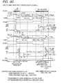
- the first-half count operation is performed at the present row when the previous row is at the low brightness level and the second-half count operation at the present row when the previous row is at the high brightness level. Accordingly, when the brightness levels of the previous row and the present row are equal to each other, the count operation period can be reduced in comparison with the case where the present embodiment is not applied, thereby reducing the power consumption.
- the comparison output COMP of the voltage comparator 252 at the signal level Ssig of the pixel signal voltage Vx of the previous row is latched and the count operation period on both the reset level Srst and the signal level Ssig of the pixel signal voltage Vx of the subsequent row is controlled on the basis of the latched phase information PCOMP. Accordingly, the second-half count operation is selected when the input level is high (bright: high brightness), and the first-half count operation is selected when the input level is low (dark: low brightness). As a result, the state where the count period is shortened and the power consumption is reduced is selected in any input level.
- the first-half count operation is performed regardless of the input level. Accordingly, the comparison process period or the count period is elongated and the power consumption is enhanced, when the pixel signal amplitude is great, but the comparison process period or the count period is shortened and the power consumption is reduced, when the pixel signal amplitude is small.
- the first-half count operation is selected when the pixel signal amplitude is small, and the second-half count operation is selected when the pixel signal amplitude is great, whereby the counter units 254 are controlled to shorten the count operation period depending on the pixel signal amplitude.
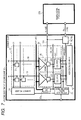
- Fig. 7 is a diagram illustrating a structure for independently controlling the counter activation period of the respective counters 254 according to a second example of the second embodiment.
- Fig. 7 is a block diagram illustrating a circuit configuration example for putting the second embodiment (second example) into practice.
- a timing diagram illustrating operations according to the second embodiment (second example) is omitted, but there is no basic difference from the operations of the second embodiment (first example), except for the amplitude determination (level determination in this example).
- the count phase adjuster 260 does not include the data storage and transmission output unit 256, unlike the second embodiment (first example).
- the phase control signal PHASE supplied from the digital signal processor 270 is supplied to the input terminal IN2 of the EX-OR gate 262.
- the EX-OR gate 262 logically inverts the comparison pulse COMP to output the inverted comparison pulse as the count enable signal EN when the phase adjustment control signal PHASE from the digital signal process 270 is at the H level, and outputs the comparison pulse COMP as the count enable signal EN without any change when the phase adjustment control signal PHASE is at the L level.
- the control on the subsequent row may be performed by determining the brightness level every row.
- the L/H of the phase adjustment control signal PHASE can be switched by rows on the basis of information indicating whether the average brightness level of one row calculated from the data output from the output circuit 28 (DPU 28a) is higher than the middle brightness level.
- the control on the subsequent picture may be performed.
- the L/H of the phase adjustment control signal PHASE can be switched by picture on the basis of information indicating whether the average brightness level of one picture calculated from the data output from the output circuit 28 (DPU 28a) is higher than the middle brightness level.
- the degree of precision is enhanced. This is because the determination is preformed using the signal level Ssig depending on the reset level Srst in the second embodiment (first example), but the determination is performed using the data having been subjected to the CDS process, that is, the digital data Dsig of the signal component Vsig excluding the influence of the reset level Srst in the second embodiment (second example).
- the imaging device 8 includes: an imaging lens 802 serving as a main part of an optical system that obtains image information by making light L carrying an image of a photographic subject Z, which is located below a light source 801, such as sunlight or a fluorescent lamp, guided toward the image apparatus and imaged; an optical low pass filter 804; a color filter group 812 in which color filters corresponding to R, G, and B, for example, are arrayed in a Bayer pattern; a pixel array unit 10; a driving controller 7 that drives the pixel array unit 10; a column processor 26 that performs the CDS process, the AD conversion process, and the like on a pixel signal output from the pixel array unit 10; and a camera signal processor 810 that processes an imaging data output from the column processor 26.
- an imaging lens 802 serving as a main part of an optical system that obtains image information by making light L carrying an image of a photographic subject Z, which is located below a light source 801, such as sunlight or a fluorescent lamp, guided toward the image apparatus and imaged
- the camera signal processor 810 includes an imaging signal processor 820 and a camera controller 900 functioning as a main controller that controls the entire imaging device 8.
- the imaging signal processor 820 includes: a signal separator 822 having a primary color separating function of separating a digital imaging signal, which is supplied from a column AD circuit 25b (refer to Fig. 1 ) of the column processor 26, into primary color signals of R (red), G (green), and B (blue) when a color filter other than a primary color filter is used; and a color signal processor 830 that performs signal processing on a color signal C on the basis of the primary color signals R, G, and B separated by the signal separator 822.
- the camera controller 900 in the present embodiment includes: a microprocessor 902 that is a core section of a computer, a representative example of which is a CPU (central processing unit) in which functions of operations and controls performed by a computer are integrated in a micro integrated circuit; a ROM (read only memory) 904 that is a storage unit for read only; a RAM (random access memory) 906 in which writing and reading are possible when needed and which is an example of a volatile storage unit; and other peripheral members not shown in the drawing.
- the microprocessor 902, the ROM 904, and the RAM 906 are collectively called a microcomputer.
- the 'volatile storage unit' means a storage unit in which the stored content is removed when an apparatus is turned off.
- the 'non-volatile storage unit' means a storage unit in which the stored content is still stored even when a main power supply of the apparatus is turned off. Any storage unit capable of persistently storing the stored content may be used as the non-volatile storage unit.
- the non-volatile storage unit is not limited to a semiconductor memory device having a non-volatile property.
- a volatile memory device may be configured to show the 'non-volatile property' by providing a backup power supply.
- the camera controller 900 is configured such that a recording medium 924, such as a memory card, can be inserted thereto or detached therefrom and configured to be able to be connected with a communication network, such as Internet.
- a recording medium 924 such as a memory card
- the camera controller 900 includes a memory reader 907 and a communication I/F (interface) 908 in addition to the microprocessor 902, the ROM 904, and the RAM 906.
- a program for exposure control is included in the microprocessor 902, such that the camera controller 900 of the imaging device 8 also functions as an exposure condition controller that controls an exposure condition.
- the memory reader 907 stores (installs) data read from the recording medium 924 in the RAM 906.
- the communication I/F 908 middles transmission and reception of communication data between a communication network, such as Internet, and the camera controller 900.
- the imaging device 8 is shown in the form of a module in which the drive controller 7 and the column processor 26 are formed separately from the pixel array unit 10.
- the imaging device 8 may use the solid state imaging device 1 in the form of one chip in which the drive controller 7 and the column processor 26 are integrally formed on the same semiconductor substrate as the pixel array unit 10.
- the imaging device 8 is shown in a condition where an optical system, such as the imaging lens 802, the optical low pass filter 804, or an infrared light cut-off filter 805, is also included in addition to the pixel array unit 10, the driving controller 7, the column processor 26, or the camera signal processor 810.
- an optical system such as the imaging lens 802, the optical low pass filter 804, or an infrared light cut-off filter 805
- This is suitable for a case of adopting a module form having an imaging function packaged by collecting those described above.
- the entire imaging device 8 may be configured such that the solid-state imaging device 1 is provided in a module form having an imaging function in a condition where the pixel array unit 10 (imaging unit) and a signal processor (excluding a camera signal processor provided after the column processor 26) closely related with the pixel array unit 10, such as the column processor 26 having an AD conversion function or a difference (CDS) processing function, are collectively packaged and the camera signal processor 810, which is the remaining signal processor, is provided after the solid-state imaging device 1 provided in the module form.
- a signal processor excluding a camera signal processor provided after the column processor 26
- CDS difference
- the entire imaging device 8 may be configured such that the solid-state imaging device 1 is provided in a module form having an imaging function in a condition where the optical system including the pixel array unit 10 and the imaging lens 802 is collectively packaged and the camera signal processor 810 is also provided within the module in addition to the solid-state imaging device 1 provided in the module form.
- the camera signal processor 810 equivalent to the camera signal processor 200 may be included.
- the solid state imaging device 1 and the imaging device 8 may be regarded as practically the same ones.
- the comparison output COMP of the voltage comparator 252 for the signal level Ssig is latched by the latch circuit 266 and is provided as the phase information PCOMP of the comparison output COMP, and it is determined whether the first-half count operation or the second-half count operation should be performed on the basis of the phase information PCOMP for both the P-phase process and the D-phase process of the subsequent row.
- this is only an example.
- latch circuits 266_P and 266_D (not shown in Figures) which latch the comparison outputs COMP of the voltage comparator 252, respectively, for each the P-phase (reset level Srst) and the D-phase (signal level Ssig) are provided.
- the latch timing at the time of P-phase process corresponds to a middle level in a maximum range of the resent level Srst.
- the timing is set at a point of 64 clocks after the initiation of change in the reference signal SLP_ADC. Then, in the subsequent P-phase process, it is determined whether the first-half count operation or the second-half count operation should be performed on the basis of a phase information COMP_PH_P latched by the latch circuit 266_P, or in the subsequent D-phase process, it is determined whether the first-half count operation or the second-half count operation should be performed on the basis of the phase information COMP_PH_D latched by the latch circuit 266_D. In this manner, the effect of reducing the power consumption can be achieved even in the P-phase process.
- a circuit configuration in the columns becomes complicate due to a factor that the P-phase process and the D-phase process do not always perform the count operation at the same phase relationship in order to give a configuration allowing the difference process (CDS process) between the P-phase process result and the D-phase process result in the columns, together with the other factor of a structure for data correction for the second-half count process (complement number count process).
- CDS process difference process
- This matter may be handled by, as adopted in the second configuration example shown in Fig. 2B , the digital calculator 29 by transmitting the P-phase process result Dp (indicating Drst) and the D-phase process result Dd (indicating Drst+Dsig) each to the digital calculator 29.
- the level determination of the pixel signal voltage Vx is performed in the processing row just prior to the present row.
- a method of determining the input level of the present processing signal for the signal to be subjected to the level determination and performing the count phase control on the basis of the determination result may be employed.
- the method is combined with the structure for determining to perform the first-half count operation or the second-half count operation depending on the P phase (that is, reset level Srst) or the D phase (that is, the signal level Ssig).
- the DA conversion circuit 27a sets the reference signal SLP_ADC to the value corresponding to the middle level of the reset level Srst or the signal level Ssig and then supplies the set signal to the voltage comparator 252.
- the comparison output COMP of the voltage comparator 252 is at the L level.
- the comparison output COMP of the voltage comparator 252 is at the H level.
- the AD conversion circuit (AD converter; column AD circuit 25 in the examples) including the comparator comparing the AD-conversion reference signal with an electrical signal corresponding to the processing signal and the counter unit performing the count process in one mode of the down-count mode and the up-count mode at the same time as the comparison process of the comparator and storing the count value acquired through the first-half count operation or the second-half count operation is applied as a data processor to the solid-state imaging device or the imaging device.
- the structure of the AD conversion circuit or the data processor may be applied to all electronic apparatuses requiring the data processing structure for acquiring digital data of analog information, as well as the solid-state imaging device or the imaging device.
Landscapes
- Engineering & Computer Science (AREA)
- Multimedia (AREA)
- Signal Processing (AREA)
- Theoretical Computer Science (AREA)
- Transforming Light Signals Into Electric Signals (AREA)
- Analogue/Digital Conversion (AREA)
Priority Applications (1)
| Application Number | Priority Date | Filing Date | Title |
|---|---|---|---|
| EP12002871.7A EP2482462B1 (de) | 2007-10-12 | 2008-10-10 | Datenprozessor, Festkörperabbildungsvorrichtung, Abbildungsvorrichtung und elektronisches Gerät |
Applications Claiming Priority (1)
| Application Number | Priority Date | Filing Date | Title |
|---|---|---|---|
| JP2007266227A JP4952498B2 (ja) | 2006-10-13 | 2007-10-12 | データ処理装置、固体撮像装置、撮像装置、電子機器 |
Related Child Applications (2)
| Application Number | Title | Priority Date | Filing Date |
|---|---|---|---|
| EP12002871.7A Division EP2482462B1 (de) | 2007-10-12 | 2008-10-10 | Datenprozessor, Festkörperabbildungsvorrichtung, Abbildungsvorrichtung und elektronisches Gerät |
| EP12002871.7 Division-Into | 2012-04-24 |
Publications (3)
| Publication Number | Publication Date |
|---|---|
| EP2048786A2 true EP2048786A2 (de) | 2009-04-15 |
| EP2048786A3 EP2048786A3 (de) | 2010-04-14 |
| EP2048786B1 EP2048786B1 (de) | 2012-06-20 |
Family
ID=40148627
Family Applications (2)
| Application Number | Title | Priority Date | Filing Date |
|---|---|---|---|
| EP08017815A Ceased EP2048786B1 (de) | 2007-10-12 | 2008-10-10 | Datenprozessor, Festkörperabbildungsvorrichtung, Abbildungsvorrichtung und elektronisches Gerät |
| EP12002871.7A Ceased EP2482462B1 (de) | 2007-10-12 | 2008-10-10 | Datenprozessor, Festkörperabbildungsvorrichtung, Abbildungsvorrichtung und elektronisches Gerät |
Family Applications After (1)
| Application Number | Title | Priority Date | Filing Date |
|---|---|---|---|
| EP12002871.7A Ceased EP2482462B1 (de) | 2007-10-12 | 2008-10-10 | Datenprozessor, Festkörperabbildungsvorrichtung, Abbildungsvorrichtung und elektronisches Gerät |
Country Status (5)
| Country | Link |
|---|---|
| US (3) | US7952630B2 (de) |
| EP (2) | EP2048786B1 (de) |
| KR (1) | KR101524737B1 (de) |
| CN (2) | CN101409772B (de) |
| TW (1) | TWI399088B (de) |
Cited By (3)
| Publication number | Priority date | Publication date | Assignee | Title |
|---|---|---|---|---|
| EP2109223A3 (de) * | 2008-04-09 | 2011-12-14 | CMOSIS nv | Analog-Digital-Umwandlung bei Pixelarrays |
| US8446309B2 (en) | 2009-02-19 | 2013-05-21 | Cmosis Nv | Analog-to-digital conversion in pixel arrays |
| CN112750401A (zh) * | 2018-11-12 | 2021-05-04 | 成都晶砂科技有限公司 | 显示驱动装置及方法 |
Families Citing this family (66)
| Publication number | Priority date | Publication date | Assignee | Title |
|---|---|---|---|---|
| US8131026B2 (en) | 2004-04-16 | 2012-03-06 | Validity Sensors, Inc. | Method and apparatus for fingerprint image reconstruction |
| DE602005022900D1 (de) | 2004-10-04 | 2010-09-23 | Validity Sensors Inc | Fingerabdruckerfassende konstruktionen mit einem substrat |
| TWI399088B (zh) * | 2007-10-12 | 2013-06-11 | Sony Corp | 資料處理器,固態成像裝置,成像裝置,及電子設備 |
| KR101504515B1 (ko) * | 2008-02-01 | 2015-03-20 | 삼성전자주식회사 | 카운터 어레이 및 이를 포함하는 이미지 센서 |
| US8116540B2 (en) | 2008-04-04 | 2012-02-14 | Validity Sensors, Inc. | Apparatus and method for reducing noise in fingerprint sensing circuits |
| JP5332314B2 (ja) * | 2008-05-29 | 2013-11-06 | ソニー株式会社 | 固体撮像素子およびカメラシステム |
| EP2321764A4 (de) | 2008-07-22 | 2012-10-10 | Validity Sensors Inc | System, vorrichtung und verfahren zur sicherung einer gerätekomponente |
| US8253809B2 (en) * | 2008-08-27 | 2012-08-28 | Sony Corporation | Analog-digital converter, analog-digital conversion method, image pickup device, method of driving the same, and camera |
| US8600122B2 (en) | 2009-01-15 | 2013-12-03 | Validity Sensors, Inc. | Apparatus and method for culling substantially redundant data in fingerprint sensing circuits |
| FR2943199B1 (fr) * | 2009-03-13 | 2012-12-28 | E2V Semiconductors | Procede de lecture de signal de capteur d'image et capteur d'image. |
| JP5429547B2 (ja) * | 2009-10-02 | 2014-02-26 | ソニー株式会社 | 固体撮像装置、撮像装置、ad変換方法 |
| US8716613B2 (en) | 2010-03-02 | 2014-05-06 | Synaptics Incoporated | Apparatus and method for electrostatic discharge protection |
| JP5507309B2 (ja) * | 2010-03-30 | 2014-05-28 | 本田技研工業株式会社 | 信号処理方法及び固体撮像装置 |
| US9001040B2 (en) | 2010-06-02 | 2015-04-07 | Synaptics Incorporated | Integrated fingerprint sensor and navigation device |
| TWI458349B (zh) * | 2010-07-26 | 2014-10-21 | Sony Corp | 固態成像裝置及攝影系統 |
| JP2012049597A (ja) * | 2010-08-24 | 2012-03-08 | Nikon Corp | 撮像装置 |
| KR101710109B1 (ko) | 2010-10-20 | 2017-02-27 | 삼성전자주식회사 | 아날로그 디지털 컨버터 및 이를 포함하는 이미지 센서 |
| US8538097B2 (en) | 2011-01-26 | 2013-09-17 | Validity Sensors, Inc. | User input utilizing dual line scanner apparatus and method |
| US8594393B2 (en) | 2011-01-26 | 2013-11-26 | Validity Sensors | System for and method of image reconstruction with dual line scanner using line counts |
| KR101936971B1 (ko) * | 2011-03-30 | 2019-01-09 | 소니 주식회사 | A/d 변환기, 고체 촬상 장치 및 구동 방법, 및 전자 기기 |
| JP5784377B2 (ja) * | 2011-06-14 | 2015-09-24 | オリンパス株式会社 | Ad変換回路および撮像装置 |
| JP5858695B2 (ja) * | 2011-09-08 | 2016-02-10 | キヤノン株式会社 | 固体撮像装置及び固体撮像装置の駆動方法 |
| JP5943576B2 (ja) * | 2011-10-07 | 2016-07-05 | キヤノン株式会社 | 固体撮像装置及び固体撮像装置の駆動方法 |
| JP6056126B2 (ja) * | 2011-10-21 | 2017-01-11 | ソニー株式会社 | 固体撮像装置およびカメラシステム |
| JP5865272B2 (ja) * | 2012-03-30 | 2016-02-17 | キヤノン株式会社 | 光電変換装置および撮像システム |
| JP5847737B2 (ja) * | 2012-03-30 | 2016-01-27 | キヤノン株式会社 | 光電変換装置および撮像システム |
| TW201408065A (zh) * | 2012-08-08 | 2014-02-16 | Novatek Microelectronics Corp | 影像感測器及其行類比數位轉換器 |
| CN103595410A (zh) * | 2012-08-17 | 2014-02-19 | 联咏科技股份有限公司 | 图像传感器及其列模数转换器 |
| GB201300999D0 (en) * | 2013-01-21 | 2013-03-06 | Cmosis Nv | Analog-to-digital conversation in pixel arrays |
| CN103051848B (zh) * | 2013-01-21 | 2015-12-09 | 长春长光辰芯光电技术有限公司 | 图像数据模数转换方法及图像传感器 |
| TWI634791B (zh) * | 2013-02-27 | 2018-09-01 | 新力股份有限公司 | Solid-state imaging device, driving method, and electronic device |
| JP6478467B2 (ja) * | 2013-03-28 | 2019-03-06 | キヤノン株式会社 | 撮像装置、撮像装置の駆動方法、撮像システム |
| JP6226551B2 (ja) * | 2013-05-08 | 2017-11-08 | キヤノン株式会社 | 撮像装置 |
| JP2015037206A (ja) * | 2013-08-12 | 2015-02-23 | キヤノン株式会社 | 撮像装置 |
| US9813652B2 (en) | 2013-08-29 | 2017-11-07 | Sony Corporation | CMOS image sensor and imaging method implementing correlated double sampling and compression |
| US9077924B2 (en) * | 2013-08-29 | 2015-07-07 | Sony Corporation | CMOS image sensor implementing correlated double sampling with compression |
| JP6486001B2 (ja) * | 2013-12-25 | 2019-03-20 | キヤノン株式会社 | Ad変換器、ad変換装置、光電変換装置、撮像システム、およびad変換方法 |
| JP2015162751A (ja) * | 2014-02-26 | 2015-09-07 | キヤノン株式会社 | 光電変換装置および撮像システム |
| JP2015216625A (ja) * | 2014-04-22 | 2015-12-03 | キヤノン株式会社 | 撮像素子及び撮像装置 |
| US9609653B2 (en) * | 2014-10-15 | 2017-03-28 | National Instruments Corporation | Spectral stitching method to increase instantaneous bandwidth in vector signal generators |
| KR102261587B1 (ko) * | 2014-12-05 | 2021-06-04 | 삼성전자주식회사 | 로우 코드 영역의 비선형성을 개선할 수 있는 이미지 센서, 이의 작동 방법, 및 이를 포함하는 장치 |
| JPWO2016151837A1 (ja) * | 2015-03-26 | 2018-01-18 | オリンパス株式会社 | 固体撮像装置 |
| KR102324537B1 (ko) | 2015-06-12 | 2021-11-09 | 삼성전자주식회사 | 출력 피크 전류를 분산할 수 있는 이미지 센서와 이를 포함하는 이미지 처리 시스템 |
| KR102386907B1 (ko) * | 2015-09-10 | 2022-04-14 | 삼성전자주식회사 | 반도체 집적 회로 |
| KR102332942B1 (ko) * | 2015-11-27 | 2021-12-01 | 에스케이하이닉스 주식회사 | 전력 소모 감소를 위한 카운팅 장치 및 그를 이용한 아날로그-디지털 변환 장치와 씨모스 이미지 센서 |
| JP2017126833A (ja) * | 2016-01-12 | 2017-07-20 | 株式会社リコー | 光電変換素子、画像読取装置、画像形成装置及び画像読取方法 |
| JPWO2017158678A1 (ja) * | 2016-03-14 | 2019-01-17 | オリンパス株式会社 | Ad変換器およびイメージセンサ |
| CN113132660B (zh) * | 2016-05-20 | 2024-09-13 | 株式会社尼康 | 摄像元件及摄像装置 |
| JP7073260B2 (ja) | 2016-08-08 | 2022-05-23 | ソニーセミコンダクタソリューションズ株式会社 | 撮像装置、電子機器 |
| JP2018113637A (ja) * | 2017-01-13 | 2018-07-19 | ソニーセミコンダクタソリューションズ株式会社 | 固体撮像素子および電子機器 |
| CN110463189B (zh) * | 2017-03-29 | 2022-11-01 | 株式会社尼康 | 摄像元件及电子相机 |
| US10347667B2 (en) * | 2017-07-26 | 2019-07-09 | International Business Machines Corporation | Thin-film negative differential resistance and neuronal circuit |
| JP6783732B2 (ja) * | 2017-09-15 | 2020-11-11 | 株式会社東芝 | 画像処理装置および画像処理方法 |
| US10785423B2 (en) * | 2017-12-07 | 2020-09-22 | Canon Kabushiki Kaisha | Image sensor, image capturing apparatus, and image capturing method |
| KR102474449B1 (ko) * | 2018-03-07 | 2022-12-06 | 삼성전자주식회사 | 이미지 센서 및 이를 포함하는 전자 시스템 |
| JP7309847B2 (ja) * | 2018-09-05 | 2023-07-18 | キーサイト テクノロジーズ, インク. | アンテナアレイのリモート無線制御用の近接場アンテナ |
| JP7227777B2 (ja) * | 2019-02-04 | 2023-02-22 | キヤノン株式会社 | 撮像装置 |
| JP7336217B2 (ja) * | 2019-03-12 | 2023-08-31 | キヤノン株式会社 | 情報処理装置、撮像素子、撮像装置、及び情報処理方法 |
| CN109754763B (zh) * | 2019-03-27 | 2020-11-20 | 合肥京东方光电科技有限公司 | 背光驱动模组及其工作方法、和显示装置 |
| KR102856356B1 (ko) * | 2019-10-21 | 2025-09-04 | 삼성전자주식회사 | 지연 회로와 보상기를 포함하는 아날로그 디지털 컨버터, 이를 포함하는 이미지 센서 및 이의 동작 방법 |
| KR102701567B1 (ko) | 2020-08-21 | 2024-08-30 | 선전 구딕스 테크놀로지 컴퍼니, 리미티드 | 이미지 센서, 지문 검출 장치 및 전자 장치 |
| CN111741240B (zh) * | 2020-08-21 | 2020-12-22 | 深圳市汇顶科技股份有限公司 | 图像传感器、指纹检测装置和电子设备 |
| CN113628304B (zh) * | 2021-10-09 | 2021-12-03 | 湖北芯擎科技有限公司 | 图像处理方法、装置、电子设备及存储介质 |
| US12028632B2 (en) | 2021-11-26 | 2024-07-02 | Samsung Electronics Co., Ltd. | Image sensor with data buffer clusters |
| CN115138208B (zh) * | 2022-09-06 | 2022-11-25 | 山东超华环保智能装备有限公司 | 数据处理器及包含该处理器的一种废气智能处理系统 |
| TWI855866B (zh) * | 2023-09-18 | 2024-09-11 | 華碩電腦股份有限公司 | 電子裝置以及其影像處理方法 |
Citations (4)
| Publication number | Priority date | Publication date | Assignee | Title |
|---|---|---|---|---|
| JP2005278135A (ja) | 2004-02-23 | 2005-10-06 | Sony Corp | 固体撮像装置および固体撮像装置の駆動方法 |
| JP2005311933A (ja) | 2004-04-26 | 2005-11-04 | Sony Corp | カウンタ回路、ad変換方法およびad変換装置、並びに物理量分布検知の半導体装置および電子機器 |
| JP2006033452A (ja) | 2004-07-16 | 2006-02-02 | Sony Corp | データ処理方法およびデータ処理装置並びに物理量分布検知の半導体装置および電子機器 |
| JP2007266227A (ja) | 2006-03-28 | 2007-10-11 | Tdk Corp | ダイシングシートの貼付方法 |
Family Cites Families (12)
| Publication number | Priority date | Publication date | Assignee | Title |
|---|---|---|---|---|
| US5877715A (en) * | 1997-06-12 | 1999-03-02 | International Business Machines Corporation | Correlated double sampling with up/down counter |
| US6583817B1 (en) * | 1998-06-24 | 2003-06-24 | Taiwan Advanced Sensors Corp. | Autocalibration of the A/D converter within the CMOS type image sensor |
| US8169517B2 (en) * | 2001-03-26 | 2012-05-01 | Panavision Imaging Llc | Image sensor ADC and CDS per column with oversampling |
| US7305329B2 (en) * | 2002-11-14 | 2007-12-04 | FRIEDMAN Jeffrey | Method for lobby and common area interior |
| JP4311181B2 (ja) * | 2003-12-05 | 2009-08-12 | ソニー株式会社 | 半導体装置の制御方法および信号処理方法並びに半導体装置および電子機器 |
| CN100474599C (zh) * | 2004-02-23 | 2009-04-01 | 索尼株式会社 | 固态图像拾取设备及其驱动的方法 |
| US7129883B2 (en) * | 2004-02-23 | 2006-10-31 | Sony Corporation | Method and apparatus for AD conversion, semiconductor device for detecting distribution of physical quantity, and electronic apparatus |
| JP4193768B2 (ja) * | 2004-07-16 | 2008-12-10 | ソニー株式会社 | データ処理方法並びに物理量分布検知の半導体装置および電子機器 |
| US7106239B1 (en) * | 2005-08-03 | 2006-09-12 | Qualcomm Incorporated | Rail-to-rail delay line for time analog-to-digital converters |
| JP4845466B2 (ja) * | 2005-10-04 | 2011-12-28 | 富士フイルム株式会社 | 固体撮像装置 |
| US7755017B2 (en) * | 2006-10-13 | 2010-07-13 | Sony Corporation | Solid-image-pickup device, image-pickup device, and method of driving solid-image-pickup device |
| TWI399088B (zh) * | 2007-10-12 | 2013-06-11 | Sony Corp | 資料處理器,固態成像裝置,成像裝置,及電子設備 |
-
2008
- 2008-10-03 TW TW097138210A patent/TWI399088B/zh not_active IP Right Cessation
- 2008-10-06 US US12/246,026 patent/US7952630B2/en not_active Expired - Fee Related
- 2008-10-10 EP EP08017815A patent/EP2048786B1/de not_active Ceased
- 2008-10-10 EP EP12002871.7A patent/EP2482462B1/de not_active Ceased
- 2008-10-10 KR KR1020080099866A patent/KR101524737B1/ko not_active Expired - Fee Related
- 2008-10-13 CN CN2008101618970A patent/CN101409772B/zh not_active Expired - Fee Related
- 2008-10-13 CN CN201110168031.4A patent/CN102263913B/zh not_active Expired - Fee Related
-
2011
- 2011-05-24 US US13/114,345 patent/US8866946B2/en not_active Expired - Fee Related
-
2014
- 2014-09-09 US US14/481,713 patent/US9374097B2/en not_active Expired - Fee Related
Patent Citations (4)
| Publication number | Priority date | Publication date | Assignee | Title |
|---|---|---|---|---|
| JP2005278135A (ja) | 2004-02-23 | 2005-10-06 | Sony Corp | 固体撮像装置および固体撮像装置の駆動方法 |
| JP2005311933A (ja) | 2004-04-26 | 2005-11-04 | Sony Corp | カウンタ回路、ad変換方法およびad変換装置、並びに物理量分布検知の半導体装置および電子機器 |
| JP2006033452A (ja) | 2004-07-16 | 2006-02-02 | Sony Corp | データ処理方法およびデータ処理装置並びに物理量分布検知の半導体装置および電子機器 |
| JP2007266227A (ja) | 2006-03-28 | 2007-10-11 | Tdk Corp | ダイシングシートの貼付方法 |
Non-Patent Citations (1)
| Title |
|---|
| W. YANG ET AL.: "An Integrated 800x600 CMOS Image System, ISSCC Digest of Technical Papers", February 1999, pages: 304 - 305 |
Cited By (7)
| Publication number | Priority date | Publication date | Assignee | Title |
|---|---|---|---|---|
| EP2109223A3 (de) * | 2008-04-09 | 2011-12-14 | CMOSIS nv | Analog-Digital-Umwandlung bei Pixelarrays |
| US8253617B2 (en) | 2008-04-09 | 2012-08-28 | Cmosis Nv | Analog-to-digital conversion in pixel arrays |
| US8253616B2 (en) | 2008-04-09 | 2012-08-28 | Cmosis Nv | Analog-to-digital conversion in pixel arrays using a ramp signal having a single cycle |
| EP2571167A1 (de) * | 2008-04-09 | 2013-03-20 | Cmosis NV | Analog-Digital-Umwandlung bei Pixelarrays |
| US8446309B2 (en) | 2009-02-19 | 2013-05-21 | Cmosis Nv | Analog-to-digital conversion in pixel arrays |
| CN112750401A (zh) * | 2018-11-12 | 2021-05-04 | 成都晶砂科技有限公司 | 显示驱动装置及方法 |
| CN112750401B (zh) * | 2018-11-12 | 2022-05-24 | 成都晶砂科技有限公司 | 显示驱动装置及方法 |
Also Published As
| Publication number | Publication date |
|---|---|
| US7952630B2 (en) | 2011-05-31 |
| CN101409772B (zh) | 2011-08-17 |
| CN102263913A (zh) | 2011-11-30 |
| US20150009387A1 (en) | 2015-01-08 |
| CN101409772A (zh) | 2009-04-15 |
| US9374097B2 (en) | 2016-06-21 |
| TWI399088B (zh) | 2013-06-11 |
| KR20090037836A (ko) | 2009-04-16 |
| KR101524737B1 (ko) | 2015-06-01 |
| US20090109315A1 (en) | 2009-04-30 |
| EP2048786B1 (de) | 2012-06-20 |
| TW200935886A (en) | 2009-08-16 |
| EP2048786A3 (de) | 2010-04-14 |
| CN102263913B (zh) | 2015-12-16 |
| EP2482462A1 (de) | 2012-08-01 |
| US8866946B2 (en) | 2014-10-21 |
| EP2482462B1 (de) | 2019-03-27 |
| US20110221942A1 (en) | 2011-09-15 |
Similar Documents
| Publication | Publication Date | Title |
|---|---|---|
| EP2048786B1 (de) | Datenprozessor, Festkörperabbildungsvorrichtung, Abbildungsvorrichtung und elektronisches Gerät | |
| US7642947B2 (en) | Data processing method, data processing device, solid-state imaging device, imaging apparatus, and electronic device | |
| JP4786631B2 (ja) | 固体撮像装置、撮像装置 | |
| JP3904111B2 (ja) | 固体撮像装置及びその信号処理方法 | |
| US8031241B2 (en) | Solid-state imaging device and imaging apparatus | |
| US8072522B2 (en) | Solid-state imaging device, imaging apparatus, and electronic apparatus | |
| EP2104235B1 (de) | Analog-Digital-Umsetzer, Analog-Digital-Umsetzungsverfahren, Festkörperbildaufnahmevorrichtung. | |
| JP5347341B2 (ja) | 固体撮像装置、撮像装置、電子機器、ad変換装置、ad変換方法 | |
| US8659693B2 (en) | Solid-state image pickup element and camera system | |
| JP4379504B2 (ja) | 固体撮像素子、およびカメラシステム | |
| JP4952498B2 (ja) | データ処理装置、固体撮像装置、撮像装置、電子機器 | |
| CN104202543A (zh) | 数据处理方法、数据处理设备、半导体装置和电子设备 | |
| KR20080033890A (ko) | 고체 촬상 장치, 촬상 장치, 및 고체 촬상 장치의 구동방법 | |
| JP2013051497A (ja) | 固体撮像装置、撮像装置および撮像方法 | |
| JP5293052B2 (ja) | 固体撮像素子 |
Legal Events
| Date | Code | Title | Description |
|---|---|---|---|
| PUAI | Public reference made under article 153(3) epc to a published international application that has entered the european phase |
Free format text: ORIGINAL CODE: 0009012 |
|
| AK | Designated contracting states |
Kind code of ref document: A2 Designated state(s): AT BE BG CH CY CZ DE DK EE ES FI FR GB GR HR HU IE IS IT LI LT LU LV MC MT NL NO PL PT RO SE SI SK TR |
|
| AX | Request for extension of the european patent |
Extension state: AL BA MK RS |
|
| PUAL | Search report despatched |
Free format text: ORIGINAL CODE: 0009013 |
|
| AK | Designated contracting states |
Kind code of ref document: A3 Designated state(s): AT BE BG CH CY CZ DE DK EE ES FI FR GB GR HR HU IE IS IT LI LT LU LV MC MT NL NO PL PT RO SE SI SK TR |
|
| AX | Request for extension of the european patent |
Extension state: AL BA MK RS |
|
| 17P | Request for examination filed |
Effective date: 20101012 |
|
| 17Q | First examination report despatched |
Effective date: 20101109 |
|
| AKX | Designation fees paid |
Designated state(s): DE FR GB |
|
| GRAP | Despatch of communication of intention to grant a patent |
Free format text: ORIGINAL CODE: EPIDOSNIGR1 |
|
| GRAS | Grant fee paid |
Free format text: ORIGINAL CODE: EPIDOSNIGR3 |
|
| GRAA | (expected) grant |
Free format text: ORIGINAL CODE: 0009210 |
|
| AK | Designated contracting states |
Kind code of ref document: B1 Designated state(s): DE FR GB |
|
| REG | Reference to a national code |
Ref country code: GB Ref legal event code: FG4D |
|
| REG | Reference to a national code |
Ref country code: DE Ref legal event code: R096 Ref document number: 602008016367 Country of ref document: DE Effective date: 20120823 |
|
| PLBE | No opposition filed within time limit |
Free format text: ORIGINAL CODE: 0009261 |
|
| STAA | Information on the status of an ep patent application or granted ep patent |
Free format text: STATUS: NO OPPOSITION FILED WITHIN TIME LIMIT |
|
| 26N | No opposition filed |
Effective date: 20130321 |
|
| REG | Reference to a national code |
Ref country code: DE Ref legal event code: R097 Ref document number: 602008016367 Country of ref document: DE Effective date: 20130321 |
|
| REG | Reference to a national code |
Ref country code: FR Ref legal event code: PLFP Year of fee payment: 8 |
|
| REG | Reference to a national code |
Ref country code: FR Ref legal event code: PLFP Year of fee payment: 9 |
|
| REG | Reference to a national code |
Ref country code: FR Ref legal event code: PLFP Year of fee payment: 10 |
|
| REG | Reference to a national code |
Ref country code: FR Ref legal event code: PLFP Year of fee payment: 11 |
|
| PGFP | Annual fee paid to national office [announced via postgrant information from national office to epo] |
Ref country code: FR Payment date: 20201022 Year of fee payment: 13 |
|
| REG | Reference to a national code |
Ref country code: GB Ref legal event code: 746 Effective date: 20211108 |
|
| PG25 | Lapsed in a contracting state [announced via postgrant information from national office to epo] |
Ref country code: FR Free format text: LAPSE BECAUSE OF NON-PAYMENT OF DUE FEES Effective date: 20211031 |
|
| PGFP | Annual fee paid to national office [announced via postgrant information from national office to epo] |
Ref country code: GB Payment date: 20220922 Year of fee payment: 15 |
|
| PGFP | Annual fee paid to national office [announced via postgrant information from national office to epo] |
Ref country code: DE Payment date: 20220616 Year of fee payment: 15 |
|
| P01 | Opt-out of the competence of the unified patent court (upc) registered |
Effective date: 20230527 |
|
| REG | Reference to a national code |
Ref country code: DE Ref legal event code: R119 Ref document number: 602008016367 Country of ref document: DE |
|
| GBPC | Gb: european patent ceased through non-payment of renewal fee |
Effective date: 20231010 |
|
| PG25 | Lapsed in a contracting state [announced via postgrant information from national office to epo] |
Ref country code: GB Free format text: LAPSE BECAUSE OF NON-PAYMENT OF DUE FEES Effective date: 20231010 |
|
| PG25 | Lapsed in a contracting state [announced via postgrant information from national office to epo] |
Ref country code: GB Free format text: LAPSE BECAUSE OF NON-PAYMENT OF DUE FEES Effective date: 20231010 Ref country code: DE Free format text: LAPSE BECAUSE OF NON-PAYMENT OF DUE FEES Effective date: 20240501 |