EP2033220B1 - Stack die packages - Google Patents
Stack die packages Download PDFInfo
- Publication number
- EP2033220B1 EP2033220B1 EP07809502.3A EP07809502A EP2033220B1 EP 2033220 B1 EP2033220 B1 EP 2033220B1 EP 07809502 A EP07809502 A EP 07809502A EP 2033220 B1 EP2033220 B1 EP 2033220B1
- Authority
- EP
- European Patent Office
- Prior art keywords
- integrated circuit
- circuit die
- wirebond
- electric contacts
- electrically conductive
- Prior art date
- Legal status (The legal status is an assumption and is not a legal conclusion. Google has not performed a legal analysis and makes no representation as to the accuracy of the status listed.)
- Active
Links
Images


Classifications
-
- H—ELECTRICITY
- H01—ELECTRIC ELEMENTS
- H01L—SEMICONDUCTOR DEVICES NOT COVERED BY CLASS H10
- H01L25/00—Assemblies consisting of a plurality of semiconductor or other solid state devices
- H01L25/03—Assemblies consisting of a plurality of semiconductor or other solid state devices all the devices being of a type provided for in a single subclass of subclasses H10B, H10D, H10F, H10H, H10K or H10N, e.g. assemblies of rectifier diodes
- H01L25/04—Assemblies consisting of a plurality of semiconductor or other solid state devices all the devices being of a type provided for in a single subclass of subclasses H10B, H10D, H10F, H10H, H10K or H10N, e.g. assemblies of rectifier diodes the devices not having separate containers
- H01L25/065—Assemblies consisting of a plurality of semiconductor or other solid state devices all the devices being of a type provided for in a single subclass of subclasses H10B, H10D, H10F, H10H, H10K or H10N, e.g. assemblies of rectifier diodes the devices not having separate containers the devices being of a type provided for in group H10D89/00
- H01L25/0657—Stacked arrangements of devices
-
- H—ELECTRICITY
- H01—ELECTRIC ELEMENTS
- H01L—SEMICONDUCTOR DEVICES NOT COVERED BY CLASS H10
- H01L25/00—Assemblies consisting of a plurality of semiconductor or other solid state devices
- H01L25/50—Multistep manufacturing processes of assemblies consisting of devices, the devices being individual devices of subclass H10D or integrated devices of class H10
-
- H—ELECTRICITY
- H01—ELECTRIC ELEMENTS
- H01L—SEMICONDUCTOR DEVICES NOT COVERED BY CLASS H10
- H01L2224/00—Indexing scheme for arrangements for connecting or disconnecting semiconductor or solid-state bodies and methods related thereto as covered by H01L24/00
- H01L2224/01—Means for bonding being attached to, or being formed on, the surface to be connected, e.g. chip-to-package, die-attach, "first-level" interconnects; Manufacturing methods related thereto
- H01L2224/02—Bonding areas; Manufacturing methods related thereto
- H01L2224/023—Redistribution layers [RDL] for bonding areas
-
- H—ELECTRICITY
- H01—ELECTRIC ELEMENTS
- H01L—SEMICONDUCTOR DEVICES NOT COVERED BY CLASS H10
- H01L2224/00—Indexing scheme for arrangements for connecting or disconnecting semiconductor or solid-state bodies and methods related thereto as covered by H01L24/00
- H01L2224/01—Means for bonding being attached to, or being formed on, the surface to be connected, e.g. chip-to-package, die-attach, "first-level" interconnects; Manufacturing methods related thereto
- H01L2224/10—Bump connectors; Manufacturing methods related thereto
- H01L2224/15—Structure, shape, material or disposition of the bump connectors after the connecting process
- H01L2224/16—Structure, shape, material or disposition of the bump connectors after the connecting process of an individual bump connector
- H01L2224/161—Disposition
- H01L2224/16135—Disposition the bump connector connecting between different semiconductor or solid-state bodies, i.e. chip-to-chip
- H01L2224/16145—Disposition the bump connector connecting between different semiconductor or solid-state bodies, i.e. chip-to-chip the bodies being stacked
-
- H—ELECTRICITY
- H01—ELECTRIC ELEMENTS
- H01L—SEMICONDUCTOR DEVICES NOT COVERED BY CLASS H10
- H01L2224/00—Indexing scheme for arrangements for connecting or disconnecting semiconductor or solid-state bodies and methods related thereto as covered by H01L24/00
- H01L2224/01—Means for bonding being attached to, or being formed on, the surface to be connected, e.g. chip-to-package, die-attach, "first-level" interconnects; Manufacturing methods related thereto
- H01L2224/26—Layer connectors, e.g. plate connectors, solder or adhesive layers; Manufacturing methods related thereto
- H01L2224/31—Structure, shape, material or disposition of the layer connectors after the connecting process
- H01L2224/32—Structure, shape, material or disposition of the layer connectors after the connecting process of an individual layer connector
- H01L2224/321—Disposition
- H01L2224/32135—Disposition the layer connector connecting between different semiconductor or solid-state bodies, i.e. chip-to-chip
- H01L2224/32145—Disposition the layer connector connecting between different semiconductor or solid-state bodies, i.e. chip-to-chip the bodies being stacked
-
- H—ELECTRICITY
- H01—ELECTRIC ELEMENTS
- H01L—SEMICONDUCTOR DEVICES NOT COVERED BY CLASS H10
- H01L2224/00—Indexing scheme for arrangements for connecting or disconnecting semiconductor or solid-state bodies and methods related thereto as covered by H01L24/00
- H01L2224/01—Means for bonding being attached to, or being formed on, the surface to be connected, e.g. chip-to-package, die-attach, "first-level" interconnects; Manufacturing methods related thereto
- H01L2224/42—Wire connectors; Manufacturing methods related thereto
- H01L2224/44—Structure, shape, material or disposition of the wire connectors prior to the connecting process
- H01L2224/45—Structure, shape, material or disposition of the wire connectors prior to the connecting process of an individual wire connector
- H01L2224/45001—Core members of the connector
- H01L2224/45099—Material
- H01L2224/451—Material with a principal constituent of the material being a metal or a metalloid, e.g. boron (B), silicon (Si), germanium (Ge), arsenic (As), antimony (Sb), tellurium (Te) and polonium (Po), and alloys thereof
- H01L2224/45138—Material with a principal constituent of the material being a metal or a metalloid, e.g. boron (B), silicon (Si), germanium (Ge), arsenic (As), antimony (Sb), tellurium (Te) and polonium (Po), and alloys thereof the principal constituent melting at a temperature of greater than or equal to 950°C and less than 1550°C
- H01L2224/45144—Gold (Au) as principal constituent
-
- H—ELECTRICITY
- H01—ELECTRIC ELEMENTS
- H01L—SEMICONDUCTOR DEVICES NOT COVERED BY CLASS H10
- H01L2224/00—Indexing scheme for arrangements for connecting or disconnecting semiconductor or solid-state bodies and methods related thereto as covered by H01L24/00
- H01L2224/01—Means for bonding being attached to, or being formed on, the surface to be connected, e.g. chip-to-package, die-attach, "first-level" interconnects; Manufacturing methods related thereto
- H01L2224/42—Wire connectors; Manufacturing methods related thereto
- H01L2224/47—Structure, shape, material or disposition of the wire connectors after the connecting process
- H01L2224/48—Structure, shape, material or disposition of the wire connectors after the connecting process of an individual wire connector
- H01L2224/481—Disposition
- H01L2224/48135—Connecting between different semiconductor or solid-state bodies, i.e. chip-to-chip
- H01L2224/48145—Connecting between different semiconductor or solid-state bodies, i.e. chip-to-chip the bodies being stacked
-
- H—ELECTRICITY
- H01—ELECTRIC ELEMENTS
- H01L—SEMICONDUCTOR DEVICES NOT COVERED BY CLASS H10
- H01L2224/00—Indexing scheme for arrangements for connecting or disconnecting semiconductor or solid-state bodies and methods related thereto as covered by H01L24/00
- H01L2224/01—Means for bonding being attached to, or being formed on, the surface to be connected, e.g. chip-to-package, die-attach, "first-level" interconnects; Manufacturing methods related thereto
- H01L2224/42—Wire connectors; Manufacturing methods related thereto
- H01L2224/47—Structure, shape, material or disposition of the wire connectors after the connecting process
- H01L2224/48—Structure, shape, material or disposition of the wire connectors after the connecting process of an individual wire connector
- H01L2224/481—Disposition
- H01L2224/48151—Connecting between a semiconductor or solid-state body and an item not being a semiconductor or solid-state body, e.g. chip-to-substrate, chip-to-passive
- H01L2224/48221—Connecting between a semiconductor or solid-state body and an item not being a semiconductor or solid-state body, e.g. chip-to-substrate, chip-to-passive the body and the item being stacked
- H01L2224/48225—Connecting between a semiconductor or solid-state body and an item not being a semiconductor or solid-state body, e.g. chip-to-substrate, chip-to-passive the body and the item being stacked the item being non-metallic, e.g. insulating substrate with or without metallisation
- H01L2224/48227—Connecting between a semiconductor or solid-state body and an item not being a semiconductor or solid-state body, e.g. chip-to-substrate, chip-to-passive the body and the item being stacked the item being non-metallic, e.g. insulating substrate with or without metallisation connecting the wire to a bond pad of the item
-
- H—ELECTRICITY
- H01—ELECTRIC ELEMENTS
- H01L—SEMICONDUCTOR DEVICES NOT COVERED BY CLASS H10
- H01L2224/00—Indexing scheme for arrangements for connecting or disconnecting semiconductor or solid-state bodies and methods related thereto as covered by H01L24/00
- H01L2224/73—Means for bonding being of different types provided for in two or more of groups H01L2224/10, H01L2224/18, H01L2224/26, H01L2224/34, H01L2224/42, H01L2224/50, H01L2224/63, H01L2224/71
- H01L2224/731—Location prior to the connecting process
-
- H—ELECTRICITY
- H01—ELECTRIC ELEMENTS
- H01L—SEMICONDUCTOR DEVICES NOT COVERED BY CLASS H10
- H01L2224/00—Indexing scheme for arrangements for connecting or disconnecting semiconductor or solid-state bodies and methods related thereto as covered by H01L24/00
- H01L2224/73—Means for bonding being of different types provided for in two or more of groups H01L2224/10, H01L2224/18, H01L2224/26, H01L2224/34, H01L2224/42, H01L2224/50, H01L2224/63, H01L2224/71
- H01L2224/732—Location after the connecting process
- H01L2224/73201—Location after the connecting process on the same surface
- H01L2224/73207—Bump and wire connectors
-
- H—ELECTRICITY
- H01—ELECTRIC ELEMENTS
- H01L—SEMICONDUCTOR DEVICES NOT COVERED BY CLASS H10
- H01L2224/00—Indexing scheme for arrangements for connecting or disconnecting semiconductor or solid-state bodies and methods related thereto as covered by H01L24/00
- H01L2224/73—Means for bonding being of different types provided for in two or more of groups H01L2224/10, H01L2224/18, H01L2224/26, H01L2224/34, H01L2224/42, H01L2224/50, H01L2224/63, H01L2224/71
- H01L2224/732—Location after the connecting process
- H01L2224/73251—Location after the connecting process on different surfaces
- H01L2224/73253—Bump and layer connectors
-
- H—ELECTRICITY
- H01—ELECTRIC ELEMENTS
- H01L—SEMICONDUCTOR DEVICES NOT COVERED BY CLASS H10
- H01L2224/00—Indexing scheme for arrangements for connecting or disconnecting semiconductor or solid-state bodies and methods related thereto as covered by H01L24/00
- H01L2224/73—Means for bonding being of different types provided for in two or more of groups H01L2224/10, H01L2224/18, H01L2224/26, H01L2224/34, H01L2224/42, H01L2224/50, H01L2224/63, H01L2224/71
- H01L2224/732—Location after the connecting process
- H01L2224/73251—Location after the connecting process on different surfaces
- H01L2224/73265—Layer and wire connectors
-
- H—ELECTRICITY
- H01—ELECTRIC ELEMENTS
- H01L—SEMICONDUCTOR DEVICES NOT COVERED BY CLASS H10
- H01L2225/00—Details relating to assemblies covered by the group H01L25/00 but not provided for in its subgroups
- H01L2225/03—All the devices being of a type provided for in the same main group of the same subclass of class H10, e.g. assemblies of rectifier diodes
- H01L2225/04—All the devices being of a type provided for in the same main group of the same subclass of class H10, e.g. assemblies of rectifier diodes the devices not having separate containers
- H01L2225/065—All the devices being of a type provided for in the same main group of the same subclass of class H10
- H01L2225/06503—Stacked arrangements of devices
- H01L2225/06506—Wire or wire-like electrical connections between devices
-
- H—ELECTRICITY
- H01—ELECTRIC ELEMENTS
- H01L—SEMICONDUCTOR DEVICES NOT COVERED BY CLASS H10
- H01L2225/00—Details relating to assemblies covered by the group H01L25/00 but not provided for in its subgroups
- H01L2225/03—All the devices being of a type provided for in the same main group of the same subclass of class H10, e.g. assemblies of rectifier diodes
- H01L2225/04—All the devices being of a type provided for in the same main group of the same subclass of class H10, e.g. assemblies of rectifier diodes the devices not having separate containers
- H01L2225/065—All the devices being of a type provided for in the same main group of the same subclass of class H10
- H01L2225/06503—Stacked arrangements of devices
- H01L2225/0651—Wire or wire-like electrical connections from device to substrate
-
- H—ELECTRICITY
- H01—ELECTRIC ELEMENTS
- H01L—SEMICONDUCTOR DEVICES NOT COVERED BY CLASS H10
- H01L2225/00—Details relating to assemblies covered by the group H01L25/00 but not provided for in its subgroups
- H01L2225/03—All the devices being of a type provided for in the same main group of the same subclass of class H10, e.g. assemblies of rectifier diodes
- H01L2225/04—All the devices being of a type provided for in the same main group of the same subclass of class H10, e.g. assemblies of rectifier diodes the devices not having separate containers
- H01L2225/065—All the devices being of a type provided for in the same main group of the same subclass of class H10
- H01L2225/06503—Stacked arrangements of devices
- H01L2225/06527—Special adaptation of electrical connections, e.g. rewiring, engineering changes, pressure contacts, layout
-
- H—ELECTRICITY
- H01—ELECTRIC ELEMENTS
- H01L—SEMICONDUCTOR DEVICES NOT COVERED BY CLASS H10
- H01L2924/00—Indexing scheme for arrangements or methods for connecting or disconnecting semiconductor or solid-state bodies as covered by H01L24/00
- H01L2924/01—Chemical elements
- H01L2924/01079—Gold [Au]
-
- H—ELECTRICITY
- H01—ELECTRIC ELEMENTS
- H01L—SEMICONDUCTOR DEVICES NOT COVERED BY CLASS H10
- H01L2924/00—Indexing scheme for arrangements or methods for connecting or disconnecting semiconductor or solid-state bodies as covered by H01L24/00
- H01L2924/10—Details of semiconductor or other solid state devices to be connected
- H01L2924/11—Device type
- H01L2924/14—Integrated circuits
Definitions
- the present invention relates generally to integrated circuit manufacture. More particularly, the present invention relates to incorporating multiple integrated circuit dies in a single package.
- US 2001/0002726 A1 relates to a semiconductor device and a method for producing same. It is aimed at providing a manufacturing method in which electrodes of the semiconductor chips of the semiconductor device are connected with each other such that damaging of a property of the respective semiconductor chip is avoided. It is further aimed at providing a ferroelectric memory chip in which the electrodes of the memory chip and the semiconductor chip are connected with each other without heating the ferroelectric memory chip beyond a predetermined temperature.
- the document further shows bonding methods such as thermosonic bonding or ultrasonic bonding allowing to mount a plurality of semiconductor chips on top of each other.
- US 2006/0097284 A1 relates to an integrated circuit die, wherein two of the bonding pads, which are located on opposite sides of the die share a common logical function.
- the invention features an integrated circuit package comprising: a substrate comprising first electric contacts; a first wirebond integrated circuit die mechanically coupled to the substrate and comprising second electric contacts electrically coupled to the first electric contacts of the substrate by first electrically conductive wires; a flip-chip integrated circuit die comprising third electric contacts electrically coupled to the second electric contacts of the first wirebond integrated circuit die by electrically conductive bumps; and a second wirebond integrated circuit die mechanically coupled to the flip-chip integrated circuit die and comprising fourth electric contacts electrically coupled to the second electric contacts of the first wirebond integrated circuit die, or the first electric contacts of the substrate, or both, by second electrically conductive wires.
- the second wirebond integrated circuit die further comprises a redistribution layer comprising fifth electric contacts disposed near a first edge of the second wirebond integrated circuit die, sixth electric contacts disposed near a second edge of the second wirebond integrated circuit die, and traces electrically coupling the fifth and sixth electric contacts, wherein the sixth electric contacts are electrically connected to the fourth electric contacts being disposed near the second edge of the second wirebond integrated circuit die.
- the first wirebond integrated circuit die comprises a system-on-a-chip (SoC) electric circuit
- the flip-chip integrated circuit die comprises a flash memory
- the second wirebond integrated circuit die comprises a synchronous dynamic random access memory (SDRAM).
- SoC system-on-a-chip
- SDRAM synchronous dynamic random access memory
- an integrated circuit package comprises a substrate, a wirebond integrated circuit die atop the substrate, a flip-chip integrated circuit die atop the wirebond integrated circuit die, and a second wirebond integrated circuit die atop the flip-chip integrated circuit die.
- the contacts of the lower wirebond integrated circuit die are wirebonded to the substrate contacts.
- the contacts of the flip-chip integrated circuit die which can be ball grid array (BGA) contacts, are connected to the contacts of the first wirebond integrated circuit die by electrically conductive bumps.
- the contacts of the upper wirebond integrated circuit die are wirebonded to the contacts of the lower wirebond integrated circuit die, or the contacts of the substrate, or both.
- BGA ball grid array
- Redistribution layers can be used atop either or both of the wirebond integrated circuit dies.
- a redistribution layer can be used atop the lower wirebond integrated circuit die to connect the electrically conductive bumps to wirebond pads on the lower wirebond integrated circuit die.
- Another redistribution layer can be used atop the upper wirebond integrated circuit die to connect the wirebond pads from one edge of the upper wirebond integrated circuit die to wirebond pads on another edge, for example when the upper wirebond integrated circuit die is so large that wirebonds are only possible from one edge.
- An adhesive can be used to mechanically couple the lower wirebond integrated circuit die to the substrate, and to mechanically couple the upper wirebond integrated circuit die to the flip-chip integrated circuit die.
- Mechanical coupling between the lower wirebond integrated circuit die and the flip-chip integrated circuit die is achieved by the electrically conductive bumps, but can be augmented by underfill techniques using an adhesive.
- the adhesives can include silver epoxy and the like.
- An encapsulant can be used to surround the stack of integrated circuit dies and the wirebond wires.
- the lower wirebond integrated circuit die comprises a system-on-a-chip (SoC) electric circuit
- the flip-chip integrated circuit die comprises a flash memory
- the upper wirebond integrated circuit die comprises a synchronous dynamic random access memory (SDRAM).
- SoC system-on-a-chip
- SDRAM synchronous dynamic random access memory
- other integrated circuits can be used.
- FIG. 1 shows a side view, not necessarily drawn to scale, of an integrated circuit package 100 comprising a stack of three integrated circuit dies according to some embodiments of the present invention.
- Integrated circuit package 100 comprises a substrate 102, a wirebond integrated circuit die 104, a flip-chip integrated circuit die 106, and a wirebond integrated circuit die 108.
- Substrate 102 has electric contacts 110 that can be connected to other devices, terminals, and the like.
- Wirebond integrated circuit die 104 has electric contacts (that is, wirebond pads) 112 that are connected by electrically conductive wires 124A to electric contacts 110 of substrate 102.
- Electrically conductive wires 124A can be implemented as gold wires and the like.
- Flip-chip integrated circuit die 106 has electric contacts (that is, balls) 114 that are connected by electrically conductive bumps 120 to wirebond pads 112 of wirebond integrated circuit die 104.
- a redistribution layer (RDL) 122 is used to connect electrically conductive bumps 120 to some or all of wirebond pads 112.
- FIG. 2 shows a top view of redistribution layer 122 of FIG. 1 according to some embodiments of the present invention.
- Redistribution layer 122 includes electric contacts (that is, bump pads) 202 for connection to respective electrically conductive bumps 120 of flip-chip integrated circuit die 106, electric contacts 204 for connection to respective wirebond pads 112 of wirebond integrated circuit die 104, and electrically conductive traces 206 connecting respective bump pads 202 and electric contacts 204.
- electric contacts that is, bump pads
- wirebond integrated circuit die 108 has electric contacts (that is, wirebond pads) 1 16.
- Wirebond pads 116 can be connected by electrically conductive wires 124B to electric contacts 110 of substrate 102, or can be connected by electrically conductive wires 124C to wirebond pads 112 of wirebond integrated circuit die 104, or both.
- Electrically conductive wires 124A-C can be implemented as gold wires and the like.
- wirebond pads 112 on wirebond integrated circuit die 104 are electrically coupled to the integrated circuit within wirebond integrated circuit die 104. But in some embodiments, some of wirebond pads 112 are not coupled to the integrated circuit, but are provided instead for connections between other elements of integrated circuit package 100. For example, some of wirebond pads 112 can be used to provide connections between balls 114 of flip-chip integrated circuit die 106 and electric contacts 110 of substrate 102. As another example, in embodiments where electrically conductive wires 124B are not used, some of wirebond pads 112 can be used to provide connections between wirebond pads 116 of wirebond integrated circuit die 108 and electric contacts 110 of substrate 102.
- Integrated circuit dies 104-108 and electrically conductive wires 124 can be surrounded by an encapsulant 126.
- FIG. 1 depicts connections on two edges of each integrated circuit die 104-108, three or more edges can be connected as shown in FIG. 1 .
- the topmost wirebond integrated circuit die 108 is so large that one or more of its edges cannot be wirebonded.
- a redistribution layer is used atop the topmost wirebond integrated circuit die 108 to connect the electric contacts 116 from the other edge.
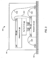
- FIG. 3 shows a side view, not necessarily drawn to scale, of an integrated circuit package 300 comprising a stack of three integrated circuit dies with a redistribution layer on the top die according to some embodiments of the present invention.
- the left edge of the top die, wirebond integrated circuit die 108 so overhangs the lower wirebond integrated circuit die 104 that wirebond connections are not possible for electric contacts 116 on that edge.
- a redistribution layer (RDL) 302 is used to connect wirebond pads 116 on the left edge to some of the wirebond pads 116 on the right edge.
- FIG. 4 shows a top view of redistribution layer 302 of FIG. 3 according to some embodiments of the present invention.
- Redistribution layer 302 includes electric contacts 402 for connection to respective wirebond pads 116 on the left edge of wirebond integrated circuit die 108, electric contacts 404 for connection to respective wirebond pads 116 on the right edge of wirebond integrated circuit die 108, and electrically conductive traces 406 connecting respective electric contacts 402 and 404.
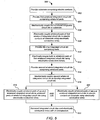
- FIG. 5 shows a process 500 for fabricating integrated circuit packages according to embodiments of the present invention.
- process 500 can be used to fabricate integrated circuit package 100 of FIG. 1 and integrated circuit package 300 of FIG. 3 .
- process 500 is discussed with reference to integrated circuit package 100 of FIG. 1 .
- the elements of process 500 are presented in one arrangement, other embodiments feature other arrangements, as will be apparent to one skilled in the relevant arts after reading this description.
- process 500 provides substrate 102 comprising electric contacts 1 10 (step 502).
- Process 500 also provides wirebond integrated circuit die 104 comprising wirebond pads 112 (step 504).
- Process 500 mechanically couples wirebond integrated circuit die 104 to substrate 102 (step 506), for example using an adhesive such as silver epoxy and the like.
- Process 500 also electrically couples wirebond pads 112 of wirebond integrated circuit die 104 to electric contacts 110 of substrate 102 using electrically conductive wires 124A (step 508).
- Process 500 also provides flip-chip integrated circuit die 106 comprising balls 114 (step 510), and electrically couples balls 114 to wirebond pads 112 of wirebond integrated circuit die 104 using electrically conductive bumps 120 (step 512).
- a redistribution layer 122 is used to electrically couple wirebond pads 112 to electrically conductive bumps 120, as described above in detail with reference to FIG. 2 .
- Process 500 also provides wirebond integrated circuit die 108 comprising wirebond pads 116 (step 514), and mechanically couples wirebond integrated circuit die 108 to flip-chip integrated circuit die 106 (step 516), for example using an adhesive such as silver epoxy and the like.
- Process 500 also electrically couples wirebond pads 116 of wirebond integrated circuit die 108 to wirebond pads 112 of wirebond integrated circuit die 104 using electrically conductive wires 124C (step 518), or electrically couples wirebond pads 116 to electric contacts 110 of substrate 102 using electrically conductive wires 124B (step 520), or both.
- a redistribution layer 302 is used to electrically couple wirebond pads 116 on one edge of wirebond integrated circuit die 108 to wirebond pads 116 on another edge, as described above in detail with reference to FIG. 4 .
- process 500 surrounds integrated circuit dies 104-108 and electrically conductive wires 124 with an encapsulant 126 (step 522).
Landscapes
- Engineering & Computer Science (AREA)
- Microelectronics & Electronic Packaging (AREA)
- Power Engineering (AREA)
- Physics & Mathematics (AREA)
- Condensed Matter Physics & Semiconductors (AREA)
- General Physics & Mathematics (AREA)
- Computer Hardware Design (AREA)
- Manufacturing & Machinery (AREA)
- Semiconductor Integrated Circuits (AREA)
- Wire Bonding (AREA)
Applications Claiming Priority (3)
| Application Number | Priority Date | Filing Date | Title |
|---|---|---|---|
| US81377806P | 2006-06-15 | 2006-06-15 | |
| US11/801,317 US7535110B2 (en) | 2006-06-15 | 2007-05-09 | Stack die packages |
| PCT/US2007/013821 WO2007146307A2 (en) | 2006-06-15 | 2007-06-13 | Stack die packages |
Publications (2)
| Publication Number | Publication Date |
|---|---|
| EP2033220A2 EP2033220A2 (en) | 2009-03-11 |
| EP2033220B1 true EP2033220B1 (en) | 2019-10-16 |
Family
ID=38666964
Family Applications (1)
| Application Number | Title | Priority Date | Filing Date |
|---|---|---|---|
| EP07809502.3A Active EP2033220B1 (en) | 2006-06-15 | 2007-06-13 | Stack die packages |
Country Status (6)
| Country | Link |
|---|---|
| US (2) | US7535110B2 (enExample) |
| EP (1) | EP2033220B1 (enExample) |
| JP (1) | JP5320611B2 (enExample) |
| CN (1) | CN101506975B (enExample) |
| TW (1) | TWI429050B (enExample) |
| WO (1) | WO2007146307A2 (enExample) |
Families Citing this family (51)
| Publication number | Priority date | Publication date | Assignee | Title |
|---|---|---|---|---|
| JP5388422B2 (ja) * | 2007-05-11 | 2014-01-15 | スパンション エルエルシー | 半導体装置及びその製造方法 |
| US7677109B2 (en) * | 2008-02-27 | 2010-03-16 | Honeywell International Inc. | Pressure sense die pad layout and method for direct wire bonding to programmable compensation integrated circuit die |
| US8310051B2 (en) | 2008-05-27 | 2012-11-13 | Mediatek Inc. | Package-on-package with fan-out WLCSP |
| US8093722B2 (en) * | 2008-05-27 | 2012-01-10 | Mediatek Inc. | System-in-package with fan-out WLCSP |
| US8896126B2 (en) | 2011-08-23 | 2014-11-25 | Marvell World Trade Ltd. | Packaging DRAM and SOC in an IC package |
| US8253231B2 (en) | 2008-09-23 | 2012-08-28 | Marvell International Ltd. | Stacked integrated circuit package using a window substrate |
| US9009393B1 (en) | 2008-09-23 | 2015-04-14 | Marvell International Ltd. | Hybrid solid-state disk (SSD)/hard disk drive (HDD) architectures |
| US20100213588A1 (en) * | 2009-02-20 | 2010-08-26 | Tung-Hsien Hsieh | Wire bond chip package |
| US8236607B2 (en) * | 2009-06-19 | 2012-08-07 | Stats Chippac Ltd. | Integrated circuit packaging system with stacked integrated circuit and method of manufacture thereof |
| US8304917B2 (en) * | 2009-12-03 | 2012-11-06 | Powertech Technology Inc. | Multi-chip stacked package and its mother chip to save interposer |
| TWI501380B (zh) * | 2010-01-29 | 2015-09-21 | Nat Chip Implementation Ct Nat Applied Res Lab | 多基板晶片模組堆疊之三維系統晶片結構 |
| KR101683814B1 (ko) | 2010-07-26 | 2016-12-08 | 삼성전자주식회사 | 관통 전극을 구비하는 반도체 장치 |
| US9490003B2 (en) * | 2011-03-31 | 2016-11-08 | Intel Corporation | Induced thermal gradients |
| US9658678B2 (en) | 2011-03-31 | 2017-05-23 | Intel Corporation | Induced thermal gradients |
| US8674483B2 (en) | 2011-06-27 | 2014-03-18 | Marvell World Trade Ltd. | Methods and arrangements relating to semiconductor packages including multi-memory dies |
| US8823165B2 (en) | 2011-07-12 | 2014-09-02 | Invensas Corporation | Memory module in a package |
| US8513817B2 (en) | 2011-07-12 | 2013-08-20 | Invensas Corporation | Memory module in a package |
| US8502390B2 (en) | 2011-07-12 | 2013-08-06 | Tessera, Inc. | De-skewed multi-die packages |
| KR101894823B1 (ko) | 2011-10-03 | 2018-09-04 | 인벤사스 코포레이션 | 평행한 윈도우를 갖는 다중-다이 와이어 본드 어셈블리를 위한 스터브 최소화 |
| US8513813B2 (en) | 2011-10-03 | 2013-08-20 | Invensas Corporation | Stub minimization using duplicate sets of terminals for wirebond assemblies without windows |
| KR20140085497A (ko) | 2011-10-03 | 2014-07-07 | 인벤사스 코포레이션 | 직교 윈도가 있는 멀티-다이 와이어본드 어셈블리를 위한 스터브 최소화 |
| US8659142B2 (en) | 2011-10-03 | 2014-02-25 | Invensas Corporation | Stub minimization for wirebond assemblies without windows |
| US8917532B2 (en) | 2011-10-03 | 2014-12-23 | Invensas Corporation | Stub minimization with terminal grids offset from center of package |
| US8436457B2 (en) | 2011-10-03 | 2013-05-07 | Invensas Corporation | Stub minimization for multi-die wirebond assemblies with parallel windows |
| US8610260B2 (en) | 2011-10-03 | 2013-12-17 | Invensas Corporation | Stub minimization for assemblies without wirebonds to package substrate |
| US8659139B2 (en) | 2011-10-03 | 2014-02-25 | Invensas Corporation | Stub minimization using duplicate sets of signal terminals in assemblies without wirebonds to package substrate |
| US8441111B2 (en) | 2011-10-03 | 2013-05-14 | Invensas Corporation | Stub minimization for multi-die wirebond assemblies with parallel windows |
| CN102446882B (zh) * | 2011-12-30 | 2013-12-04 | 北京工业大学 | 一种半导体封装中封装系统结构及制造方法 |
| US8848392B2 (en) | 2012-08-27 | 2014-09-30 | Invensas Corporation | Co-support module and microelectronic assembly |
| US8787034B2 (en) | 2012-08-27 | 2014-07-22 | Invensas Corporation | Co-support system and microelectronic assembly |
| US9368477B2 (en) | 2012-08-27 | 2016-06-14 | Invensas Corporation | Co-support circuit panel and microelectronic packages |
| US8848391B2 (en) | 2012-08-27 | 2014-09-30 | Invensas Corporation | Co-support component and microelectronic assembly |
| US9070423B2 (en) | 2013-06-11 | 2015-06-30 | Invensas Corporation | Single package dual channel memory with co-support |
| CN103426871B (zh) * | 2013-07-25 | 2017-05-31 | 上海航天测控通信研究所 | 一种高密度混合叠层封装结构及其制作方法 |
| US9123555B2 (en) | 2013-10-25 | 2015-09-01 | Invensas Corporation | Co-support for XFD packaging |
| CN103558903A (zh) * | 2013-11-12 | 2014-02-05 | 上海航天测控通信研究所 | 一种具有抗辐性能的PowerPC计算机模块 |
| US9153560B2 (en) | 2014-01-22 | 2015-10-06 | Qualcomm Incorporated | Package on package (PoP) integrated device comprising a redistribution layer |
| US9281296B2 (en) | 2014-07-31 | 2016-03-08 | Invensas Corporation | Die stacking techniques in BGA memory package for small footprint CPU and memory motherboard design |
| US9691437B2 (en) | 2014-09-25 | 2017-06-27 | Invensas Corporation | Compact microelectronic assembly having reduced spacing between controller and memory packages |
| JP2016192447A (ja) * | 2015-03-30 | 2016-11-10 | 株式会社東芝 | 半導体装置 |
| BR112017018820A2 (pt) * | 2015-04-14 | 2018-04-24 | Huawei Technologies Co., Ltd. | chip |
| US9871019B2 (en) | 2015-07-17 | 2018-01-16 | Invensas Corporation | Flipped die stack assemblies with leadframe interconnects |
| US9484080B1 (en) | 2015-11-09 | 2016-11-01 | Invensas Corporation | High-bandwidth memory application with controlled impedance loading |
| US10566310B2 (en) | 2016-04-11 | 2020-02-18 | Invensas Corporation | Microelectronic packages having stacked die and wire bond interconnects |
| US9679613B1 (en) | 2016-05-06 | 2017-06-13 | Invensas Corporation | TFD I/O partition for high-speed, high-density applications |
| US9953904B1 (en) | 2016-10-25 | 2018-04-24 | Nxp Usa, Inc. | Electronic component package with heatsink and multiple electronic components |
| CN108336030A (zh) * | 2018-01-16 | 2018-07-27 | 奥肯思(北京)科技有限公司 | 一种多层堆叠系统级封装 |
| KR102699633B1 (ko) | 2019-06-25 | 2024-08-29 | 삼성전자주식회사 | 반도체 장치 및 그 제조 방법 |
| US11075147B2 (en) * | 2019-07-08 | 2021-07-27 | Texas Instruments Incorporated | Stacked die semiconductor package |
| CN110943077A (zh) * | 2019-11-08 | 2020-03-31 | 关键禾芯科技股份有限公司 | 毫米波应用的多颗晶片封装结构 |
| US20240072002A1 (en) * | 2022-08-23 | 2024-02-29 | Micron Technology, Inc. | Semiconductor devices, assemblies, and associated methods |
Family Cites Families (19)
| Publication number | Priority date | Publication date | Assignee | Title |
|---|---|---|---|---|
| JPH0274046A (ja) * | 1988-09-09 | 1990-03-14 | Nec Ic Microcomput Syst Ltd | 半導体集積回路装置 |
| JP3602888B2 (ja) * | 1995-06-14 | 2004-12-15 | 松下電器産業株式会社 | 半導体装置 |
| US5815372A (en) * | 1997-03-25 | 1998-09-29 | Intel Corporation | Packaging multiple dies on a ball grid array substrate |
| US6271598B1 (en) * | 1997-07-29 | 2001-08-07 | Cubic Memory, Inc. | Conductive epoxy flip-chip on chip |
| JP3111312B2 (ja) * | 1997-10-29 | 2000-11-20 | ローム株式会社 | 半導体装置 |
| US6413797B2 (en) | 1997-10-09 | 2002-07-02 | Rohm Co., Ltd. | Semiconductor device and method for making the same |
| US6222260B1 (en) * | 1998-05-07 | 2001-04-24 | Vlsi Technology, Inc. | Integrated circuit device with integral decoupling capacitor |
| JP3494901B2 (ja) * | 1998-09-18 | 2004-02-09 | シャープ株式会社 | 半導体集積回路装置 |
| JP2001196529A (ja) * | 2000-01-17 | 2001-07-19 | Mitsubishi Electric Corp | 半導体装置及びその配線方法 |
| JP2001223324A (ja) * | 2000-02-10 | 2001-08-17 | Mitsubishi Electric Corp | 半導体装置 |
| JP2003197856A (ja) * | 2001-12-28 | 2003-07-11 | Oki Electric Ind Co Ltd | 半導体装置 |
| JP2003332522A (ja) * | 2002-05-17 | 2003-11-21 | Mitsubishi Electric Corp | 半導体装置 |
| US6747341B2 (en) * | 2002-06-27 | 2004-06-08 | Semiconductor Components Industries, L.L.C. | Integrated circuit and laminated leadframe package |
| JP2005109068A (ja) * | 2003-09-30 | 2005-04-21 | Sanyo Electric Co Ltd | 半導体装置およびその製造方法 |
| JP4103796B2 (ja) * | 2003-12-25 | 2008-06-18 | 沖電気工業株式会社 | 半導体チップパッケージ及びマルチチップパッケージ |
| JP2005268534A (ja) * | 2004-03-18 | 2005-09-29 | Shinko Electric Ind Co Ltd | 半導体チップおよび積層型半導体装置 |
| US20050212144A1 (en) * | 2004-03-25 | 2005-09-29 | Rugg William L | Stacked die for inclusion in standard package technology |
| US7217597B2 (en) * | 2004-06-22 | 2007-05-15 | Micron Technology, Inc. | Die stacking scheme |
| US8212367B2 (en) | 2004-11-10 | 2012-07-03 | Sandisk Il Ltd. | Integrated circuit die with logically equivalent bonding pads |
-
2007
- 2007-05-09 US US11/801,317 patent/US7535110B2/en active Active
- 2007-06-13 EP EP07809502.3A patent/EP2033220B1/en active Active
- 2007-06-13 WO PCT/US2007/013821 patent/WO2007146307A2/en not_active Ceased
- 2007-06-13 CN CN2007800304876A patent/CN101506975B/zh active Active
- 2007-06-13 JP JP2009515464A patent/JP5320611B2/ja active Active
- 2007-06-15 TW TW096121889A patent/TWI429050B/zh active
-
2009
- 2009-05-01 US US12/434,264 patent/US7825521B2/en active Active
Non-Patent Citations (1)
| Title |
|---|
| None * |
Also Published As
| Publication number | Publication date |
|---|---|
| US20090212410A1 (en) | 2009-08-27 |
| WO2007146307A2 (en) | 2007-12-21 |
| WO2007146307B1 (en) | 2008-05-22 |
| TW200807670A (en) | 2008-02-01 |
| CN101506975B (zh) | 2011-04-06 |
| TWI429050B (zh) | 2014-03-01 |
| WO2007146307A3 (en) | 2008-03-06 |
| JP5320611B2 (ja) | 2013-10-23 |
| JP2009540606A (ja) | 2009-11-19 |
| US7535110B2 (en) | 2009-05-19 |
| CN101506975A (zh) | 2009-08-12 |
| US7825521B2 (en) | 2010-11-02 |
| US20080006948A1 (en) | 2008-01-10 |
| EP2033220A2 (en) | 2009-03-11 |
Similar Documents
| Publication | Publication Date | Title |
|---|---|---|
| EP2033220B1 (en) | Stack die packages | |
| US8664780B2 (en) | Semiconductor package having plural semiconductor chips and method of forming the same | |
| US8076770B2 (en) | Semiconductor device including a first land on the wiring substrate and a second land on the sealing portion | |
| US8896130B2 (en) | Multi-chip stack structure and method for fabricating the same | |
| CN101232004A (zh) | 芯片堆叠封装结构 | |
| KR20100050750A (ko) | 실장 높이는 축소되나, 솔더 접합 신뢰도는 개선되는 웨이퍼 레벨 칩 온 칩 패키지와, 패키지 온 패키지 및 그 제조방법 | |
| US20080237833A1 (en) | Multi-chip semiconductor package structure | |
| US8680686B2 (en) | Method and system for thin multi chip stack package with film on wire and copper wire | |
| US20130069223A1 (en) | Flash memory card without a substrate and its fabrication method | |
| US20080157302A1 (en) | Stacked-package quad flat null lead package | |
| KR101685068B1 (ko) | 시스템 인 패키지 및 이의 제조방법 | |
| US20080023816A1 (en) | Semiconductor package | |
| CN106449612A (zh) | 存储器芯片堆叠封装结构 | |
| US9087883B2 (en) | Method and apparatus for stacked semiconductor chips | |
| CN202394957U (zh) | 半导体晶圆及封装构造 | |
| TWI711131B (zh) | 晶片封裝結構 | |
| CN101764126A (zh) | 无外引脚的多芯片半导体封装构造及导线架 | |
| CN101226929B (zh) | 半导体封装结构及其制造方法 | |
| US20080237831A1 (en) | Multi-chip semiconductor package structure | |
| US20110304044A1 (en) | Stacked chip package structure and its fabrication method | |
| US20080203553A1 (en) | Stackable bare-die package | |
| TWI229927B (en) | Semiconductor device with stacked package and method for fabricating the same | |
| KR20090074494A (ko) | 스택 패키지 및 그의 제조방법 | |
| CN111564379A (zh) | 芯片的封装方法及芯片结构 | |
| KR20010053953A (ko) | 멀티 칩 패키지 |
Legal Events
| Date | Code | Title | Description |
|---|---|---|---|
| PUAI | Public reference made under article 153(3) epc to a published international application that has entered the european phase |
Free format text: ORIGINAL CODE: 0009012 |
|
| 17P | Request for examination filed |
Effective date: 20081215 |
|
| AK | Designated contracting states |
Kind code of ref document: A2 Designated state(s): AT BE BG CH CY CZ DE DK EE ES FI FR GB GR HU IE IS IT LI LT LU LV MC MT NL PL PT RO SE SI SK TR |
|
| AX | Request for extension of the european patent |
Extension state: AL BA HR MK RS |
|
| DAX | Request for extension of the european patent (deleted) | ||
| RBV | Designated contracting states (corrected) |
Designated state(s): DE FR GB |
|
| 17Q | First examination report despatched |
Effective date: 20090921 |
|
| RIC1 | Information provided on ipc code assigned before grant |
Ipc: H01L 25/00 20060101ALI20190313BHEP Ipc: H01L 25/065 20060101AFI20190313BHEP |
|
| GRAP | Despatch of communication of intention to grant a patent |
Free format text: ORIGINAL CODE: EPIDOSNIGR1 |
|
| INTG | Intention to grant announced |
Effective date: 20190430 |
|
| GRAS | Grant fee paid |
Free format text: ORIGINAL CODE: EPIDOSNIGR3 |
|
| GRAA | (expected) grant |
Free format text: ORIGINAL CODE: 0009210 |
|
| AK | Designated contracting states |
Kind code of ref document: B1 Designated state(s): DE FR GB |
|
| REG | Reference to a national code |
Ref country code: GB Ref legal event code: FG4D |
|
| REG | Reference to a national code |
Ref country code: DE Ref legal event code: R096 Ref document number: 602007059371 Country of ref document: DE |
|
| REG | Reference to a national code |
Ref country code: DE Ref legal event code: R082 Ref document number: 602007059371 Country of ref document: DE Representative=s name: GRUENECKER PATENT- UND RECHTSANWAELTE PARTG MB, DE Ref country code: DE Ref legal event code: R081 Ref document number: 602007059371 Country of ref document: DE Owner name: MARVELL ASIA PTE, LTD., SG Free format text: FORMER OWNER: MARVELL WORLD TRADE LTD., ST. MICHAEL, BB |
|
| REG | Reference to a national code |
Ref country code: DE Ref legal event code: R097 Ref document number: 602007059371 Country of ref document: DE |
|
| REG | Reference to a national code |
Ref country code: GB Ref legal event code: 732E Free format text: REGISTERED BETWEEN 20200709 AND 20200715 |
|
| PLBE | No opposition filed within time limit |
Free format text: ORIGINAL CODE: 0009261 |
|
| STAA | Information on the status of an ep patent application or granted ep patent |
Free format text: STATUS: NO OPPOSITION FILED WITHIN TIME LIMIT |
|
| 26N | No opposition filed |
Effective date: 20200717 |
|
| P01 | Opt-out of the competence of the unified patent court (upc) registered |
Effective date: 20230508 |
|
| REG | Reference to a national code |
Ref country code: DE Ref legal event code: R079 Ref document number: 602007059371 Country of ref document: DE Free format text: PREVIOUS MAIN CLASS: H01L0025065000 Ipc: H10D0080300000 |
|
| PGFP | Annual fee paid to national office [announced via postgrant information from national office to epo] |
Ref country code: DE Payment date: 20250626 Year of fee payment: 19 |
|
| PGFP | Annual fee paid to national office [announced via postgrant information from national office to epo] |
Ref country code: GB Payment date: 20250617 Year of fee payment: 19 |
|
| PGFP | Annual fee paid to national office [announced via postgrant information from national office to epo] |
Ref country code: FR Payment date: 20250624 Year of fee payment: 19 |