EP2012353A2 - Verfahren und Vorrichtung für Prüfung und Fehleranalyse - Google Patents
Verfahren und Vorrichtung für Prüfung und Fehleranalyse Download PDFInfo
- Publication number
- EP2012353A2 EP2012353A2 EP08011597A EP08011597A EP2012353A2 EP 2012353 A2 EP2012353 A2 EP 2012353A2 EP 08011597 A EP08011597 A EP 08011597A EP 08011597 A EP08011597 A EP 08011597A EP 2012353 A2 EP2012353 A2 EP 2012353A2
- Authority
- EP
- European Patent Office
- Prior art keywords
- semiconductor chip
- condition
- signal
- test pattern
- image
- Prior art date
- Legal status (The legal status is an assumption and is not a legal conclusion. Google has not performed a legal analysis and makes no representation as to the accuracy of the status listed.)
- Withdrawn
Links
Images



Classifications
-
- G—PHYSICS
- G01—MEASURING; TESTING
- G01R—MEASURING ELECTRIC VARIABLES; MEASURING MAGNETIC VARIABLES
- G01R31/00—Arrangements for testing electric properties; Arrangements for locating electric faults; Arrangements for electrical testing characterised by what is being tested not provided for elsewhere
- G01R31/28—Testing of electronic circuits, e.g. by signal tracer
- G01R31/317—Testing of digital circuits
- G01R31/3181—Functional testing
- G01R31/3183—Generation of test inputs, e.g. test vectors, patterns or sequences
-
- G—PHYSICS
- G01—MEASURING; TESTING
- G01R—MEASURING ELECTRIC VARIABLES; MEASURING MAGNETIC VARIABLES
- G01R31/00—Arrangements for testing electric properties; Arrangements for locating electric faults; Arrangements for electrical testing characterised by what is being tested not provided for elsewhere
- G01R31/28—Testing of electronic circuits, e.g. by signal tracer
- G01R31/30—Marginal testing, e.g. by varying supply voltage
- G01R31/3004—Current or voltage test
- G01R31/3008—Quiescent current [IDDQ] test or leakage current test
-
- G—PHYSICS
- G01—MEASURING; TESTING
- G01R—MEASURING ELECTRIC VARIABLES; MEASURING MAGNETIC VARIABLES
- G01R27/00—Arrangements for measuring resistance, reactance, impedance, or electric characteristics derived therefrom
- G01R27/02—Measuring real or complex resistance, reactance, impedance, or other two-pole characteristics derived therefrom, e.g. time constant
-
- G—PHYSICS
- G01—MEASURING; TESTING
- G01R—MEASURING ELECTRIC VARIABLES; MEASURING MAGNETIC VARIABLES
- G01R31/00—Arrangements for testing electric properties; Arrangements for locating electric faults; Arrangements for electrical testing characterised by what is being tested not provided for elsewhere
- G01R31/26—Testing of individual semiconductor devices
-
- G—PHYSICS
- G01—MEASURING; TESTING
- G01R—MEASURING ELECTRIC VARIABLES; MEASURING MAGNETIC VARIABLES
- G01R31/00—Arrangements for testing electric properties; Arrangements for locating electric faults; Arrangements for electrical testing characterised by what is being tested not provided for elsewhere
- G01R31/28—Testing of electronic circuits, e.g. by signal tracer
- G01R31/302—Contactless testing
- G01R31/308—Contactless testing using non-ionising electromagnetic radiation, e.g. optical radiation
- G01R31/311—Contactless testing using non-ionising electromagnetic radiation, e.g. optical radiation of integrated circuits
-
- H—ELECTRICITY
- H10—SEMICONDUCTOR DEVICES; ELECTRIC SOLID-STATE DEVICES NOT OTHERWISE PROVIDED FOR
- H10P—GENERIC PROCESSES OR APPARATUS FOR THE MANUFACTURE OR TREATMENT OF DEVICES COVERED BY CLASS H10
- H10P74/00—Testing or measuring during manufacture or treatment of wafers, substrates or devices
Definitions
- This invention relates to a method and apparatus for inspection and fault analysis of a semiconductor chip. More particularly, it relates to a method and apparatus for inspecting an LSI, detecting a defective LSI chip and for locating a defective site on the LSI chip by a non-destructive narrowing for targeting (or focusing) technique (, termed "targeting narrowing technique” hereinafter).
- the methods and apparatus for inspecting a semiconductor chip are used for detecting a defective chip in order to verify acceptability/ unacceptability of a semiconductor chip.
- the methods and apparatus for fault analysis of a semiconductor chip are used to identify a defective site of a semiconductor chip, verified to be a defective chip, in order to investigate into the cause of the defect.
- the sequence of operations for fault analysis of a semiconductor chip is roughly classified into two steps. In a first step, possible defective sites on a semiconductor chip are non-destructively detected to a micrometer order (defective site targeting narrowing technique). The site thus found by the targeting narrowing technique is then subjected to a destructive physico-chemical analysis (physico-chemical analysis technique).
- a power supply voltage is supplied to an LSI chip 101 from a power supply section 107 of an LSI tester 103 via a stage 102 (step B1).
- a test pattern is then entered to the LSI chip 101, via stage 102, from a test pattern generator 106 in the LSI tester 103 (step B2).
- An IDDQ current value quiescent state power supply current value of the LSI chip 101 is measured by an IDDQ measurement section 105 of the LSI tester 103 (step B3).
- the measured value is compared to a reference value by a pass/fail decision section 104 of the LSI tester 103 to verify whether or not the IDDQ value is an abnormal current value (step B4). If the measured value is an abnormal value (YES of step B4), the chip being tested is recognized to be an IDDQ abnormal chip (step B5). If conversely the IDDQ value is not an abnormal value (NO of step B4), another test pattern is entered from the test pattern generator 106 via stage 102 to the LSI chip 101 (step B6) and an IDDQ value is measured by the IDDQ measurement section 105 (step B3) to repeat the steps as from the step B4.
- a power supply voltage is initially applied from a power supply section 207 in an LSI tester 203 via stage 209 to an LSI chip 201 (step C1).
- a test pattern verified from the outset with the related art example 1 to exhibit IDDQ abnormality, is supplied from a test pattern generator 206 in the LSI tester 203 via stage 209 to the LSI chip 201 (step C2).
- the IDDQ value (quiescent state power supply current value) of the LSI chip 201 is measured by an IDDQ measurement section 205 of the LSI tester 203.
- the measured IDDQ value is checked as to whether or not it is coincident with a value measured with the related art example 1, by way of verification of reproducibility of abnormality measurement (step C3). If the reproducibility has not been confirmed, the problem related with the LSI tester 203 or with the LSI chip 201 is first solved, after which processing is again initiated as from step C1. Meanwhile, the case where the reproducibility has been confirmed is not indicated.
- the power supply applied to the LSI chip 201 is switched from a power supply section 207 of the LSI tester 203 to a power supply section, not shown, of an IR-OBIRCH (Infrared Optical Beam Induced Resistance Change) device 202 (step C4).
- the LSI chip 201 is then scanned and illuminated by a light beam 212 from an optical system 208 in the IR-OBIRCH device 202, to display an IR-OBIRCH image on an display section 211 in the IR-OBIRCH device 202, via an IR-OBIRCH controller 210 in the IR-OBIRCH device 202 (step C5).
- the IR-OBIRCH image, displayed on the display section 211, is visually observed to detect a route of the abnormal current or a defect (step C6).
- the optical system 208 may be provided with the function of modulating the laser beam, while the IR-OBIRCH controller 210 may include a lock-in amplifier.
- an IDDQ abnormal chip may be detected by setting a reference value for an IDDQ value intermediate between the IDDQ value distribution of a normal chip and that of an abnormal chip, in such a manner that the reference value belongs to neither the distribution of the normal chip nor the distribution of the abnormal chip, as shown in Fig.8(A) .
- the step of identifying an IDDQ abnormal chip and a step of detecting an abnormal current route or a defect are carried out separately, which means a labor-consuming inefficient operation. Further, with the method and apparatus for fault analysis according to the related art example 2, it is necessary to use an expensive LSI tester, thus raising the cost.
- a method for inspection and fault analysis comprises a step of delivering a test pattern as an input to a semiconductor chip, and a step of scanning and illuminating the semiconductor chip with a laser beam, at the time of delivering the test pattern as an input.
- the semiconductor chip is heated and the resistance changes are visualized in the semiconductor chip to generate an image.
- a decision is given on the presence or absence of an abnormal current route conducting an abnormal IDDQ in the semiconductor chip, based on the image obtained on visualizing the resistance changes.
- an apparatus for detection and fault analysis includes a stage in which a semiconductor chip is mounted thereon, and a test pattern generator that supplies a test pattern via the stage to the semiconductor chip.
- An optical system has a function of modulating the laser beam. This optical system operates so that the semiconductor chip is scanned and illuminated by a modulated laser beam.
- the apparatus according to the present invention also includes a controller for taking out a signal from the semiconductor chip through a lock-in amplifier which is configured for taking out only a signal portion of a preset frequency in a signal from the semiconductor chip. The controller performs image processing of correlating the signal portion thus taken out with scanning points.
- the apparatus according to the present invention further includes a display section displaying an image based on an image signal from the controller.
- an abnormal chip may be identified even in case of a large power supply current of the normal chip.
- distributed leakage current conducted in both a normal chip and an abnormal chip, cannot be visualized, so that it is difficult to identify an IDDQ abnormal chip.
- the IR-OBIRCH method in which resistance changes in the semiconductor chip, caused by illuminating a light beam to the semiconductor chip to heat the chip, are observed, it is possible to visualize the route along which flows the current in a concentrated fashion.
- an IR-OBIRCH image may be observed at a higher speed at the time of recognizing an abnormal LSI chip than when the normal IR-OBIRCH image is observed, with the result that the IR-OBIRCH image may be observed more efficiently than with the conventional method.
- the LSI tester needed with the conventional method, may be dispensed with, and an inexpensive test pattern generator may be used, with the result that the inspection may be carried out at a low cost.
- the step of visualizing resistance changes of the semiconductor chip is carried out at the time of delivering the other test pattern.
- the step of visualizing resistance changes of the semiconductor chip carried out under a first condition. If the presence of the abnormal current route has been determined in the decision giving step, the semiconductor chip may be scanned and illuminated by a laser beam under a second condition for heating the semiconductor chip for visualizing resistance changes in the semiconductor chip. After carrying out the step of visualizing the resistance changes in the semiconductor chip under the second condition, a step of detecting a defect and an abnormal current route conducting an abnormal IDDQ in the semiconductor chip may be carried out, based on the image obtained on visualizing resistance changes in the semiconductor chip.
- the first condition is a condition with a higher speed than in the second condition.
- the first condition is one of a condition of using a laser beam of a higher modulation frequency than in the second condition, a condition of using a laser beam of a higher scanning speed, and a condition of decreasing the number of pixels of the image per picture image, or a combination thereof.
- the optical system having the function of modulating the laser beam preferably, operates so that the semiconductor chip is scanned and illuminated by the laser beam during the time the test pattern is delivered by the test pattern generator to the semiconductor chip.
- the controller confirms the presence or absence of the abnormal current route based on the image signal.
- the controller controls the test pattern generator to switch from outputting the test pattern to outputting another different test pattern in case of the absence of the abnormal current route.
- the controller subsequently may manage control for taking out a signal from the semiconductor chip through the lock-in amplifier and for correlating the signal thus taken out with scanning point(s).
- the controller preferably, exercises control for performing the operation of taking out the signal from the semiconductor chip under a first condition, and for performing the operation of taking out the signal from the semiconductor chip under a second condition if, in confirming the presence or the absence of the abnormal current route, the presence of the abnormal current route is confirmed.
- the controller preferably, exercises control for image processing for taking out a signal from the semiconductor chip under the second condition, carrying out the image processing of correlating the signal taken out with the scanning point(s), and for subsequently detecting a defect and an abnormal current route conducting the abnormal IDDQ in the semiconductor chip, based on an image signal resulting from the image processing.
- the first condition may be a condition with a higher speed than in the second condition.
- the first condition is one of a condition of using a laser beam of a higher modulation frequency than in the second condition, a condition of using a laser beam of a higher scanning speed, and a condition of decreasing the number of pixels per picture image, or a combination thereof.
- Fig.1 is a schematic block diagram showing the constitution of an apparatus for inspection and fault analysis of the first exemplary embodiment.
- An apparatus for inspection and fault analysis of the first exemplary embodiment is used for identifying an abnormal chip in a manufacture process of an LSI chip 1 (semiconductor chip), by way of inspection, and for locating a possible fault site by targeting narrowing to decide a site of fault on the abnormal chip to investigate into the cause of the fault.
- the apparatus for inspection and fault analysis includes an IR-OBIRCH device 2 and a test pattern generator 3.
- the IR-OBIRCH (Infrared Optical Beam induced Resistance Change) device 2 is used for visualizing resistance changes induced on laser beam heating, and includes a stage 4, an optical system 5, provided with the function of modulating a laser beam, an IR-OBIRCH controller 6 and a display 7.
- a stage 4 an optical system 5 provided with the function of modulating a laser beam
- an IR-OBIRCH controller 6 an IR-OBIRCH controller 6
- a display 7 As for the IR-OBIRCH device, reference is made to Patent Document 1 and Non-Patent Document 1, the entire disclosures thereof being herein incorporated by reference thereto.
- the stage 4 is a table on which to set the LSI chip 1 as a sample.
- the stage 4 is electrically connected to the test pattern generator 3 and receives a test pattern from the latter to output the test pattern received to the LSI chip 1.
- the stage 4 is configured so that a laser beam 8 from the optical system 5 provided with the function of modulating a laser beam will illuminate the back surface of the LSI chip 1.
- the stage 4 is electrically connected to and controlled in its operation by the IR-OBIRCH controller 6.
- the optical system 5 provided with the function of modulating a laser beam is an optical device operating so that the LSI chip 1 is scanned and illuminated by the modulated laser beam 8.
- the optical system 5 provided with the function of modulating a laser beam is controlled in its operation by the IR-OBIRCH controller 6.
- the IR-OBIRCH controller 6 controls the respective components of the IR-OBIRCH device 2.
- the IR-OBIRCH controller 6 mounts a lock-in amplifier, not shown, for taking out only a signal of a preset frequency in an output signal of the LSI chip 1.
- the IR-OBIRCH controller 6 takes out the modulated OBIRCH signal, from the signal from the LSI chip 1, by the lock-in amplifier, and performs image processing for correlating the OBIRCH signal, thus taken out; with scanning points.
- An image signal, corresponding to the so processed IR-OBIRCH image is output to the display 7.
- the IR-OBIRCH controller 6 checks to see whether or not there is an abnormal current route, based on the image signal corresponding to the IR-OBIRCH image.
- the IR-OBIRCH controller 6 recognizes that the chip is the IDDQ abnormal chip. If it has been verified that there does not exist the abnormal current route, the IR-OBIRCH controller 6 controls the test pattern generator 3 to switch to outputting another test pattern.
- the display 7 displays an image based on the image signal from the IR-OBIRCH controller 6.
- the test pattern generator 3 generates a test pattern (signal) for testing the LSI chip 1.
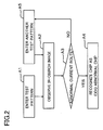
- Fig.2 depicts a flowchart for schematically illustrating the operation of the apparatus for inspection and fault analysis according to the present first exemplary embodiment.
- Fig.3 depicts a schematic view for illustrating the operation of the apparatus for inspection and fault analysis according to the present first exemplary embodiment.
- a test pattern is supplied from the test pattern generator 3 via stage 4 to the LSI chip 1 (step A1).
- An IR-OBIRCH image is visually observed on the IR-OBIRCH device 2 (step A2).
- the optical system 5 having the function of modulating the laser beam scans and illuminates the LSI chip 1 with a modulated laser beam 8.
- the optical system then takes out the modulated OBIRCH signal, via a lock-in amplifier of the IR-OBIRCH controller 6, and performs image processing for correlating the OBIRCH signal, thus taken out, with the scanning points.
- the optical system displays the IR-OBIRCH image on the display 7, based on the image-processed image signal.
- the optical system verifies whether or not there is an abnormal current route in the IR-OBIRCH image displayed (step A3).
- the decision on whether or not there is an abnormal current route is given in dependence upon whether or not there exists a contrast indicating the presence of an abnormal current route 10 in the IR-OBIRCH image.
- a contrast indicating the abnormal current route 10 in the IR-OBIRCH image.
- the difference between the normal and abnormal chips may be noticed both in case of the larger IDDQ value and in case of the smaller IDDQ value.
- laser modulation and signal takeout by the lock-in amplifier are indispensable for improving the S/N ratio.
- step A3 If it is determined that there is an abnormal current route (YES of step A3), the chip is determined to be an IDDQ abnormal chip (step A4).
- step A3 If it is determined that there is no abnormal current route (NO of step A3), the test pattern is switched to another test pattern, which is entered (step A5). The steps A2 and A3 are repeated until a decision is given that there is an abnormal current route (YES of step A3).
- steps A3 to A5 are carried out by an automatic operation by the IR-OBIRCH controller, these steps may also be carried out by a manual operation.
- an abnormal chip for which it has been difficult to identify as being an IDDQ abnormal chip, may readily be identified as such. That is, even in case of a large power supply current of a normal chip, it becomes possible to identify a given chip as being a normal chip or an abnormal chip.
- the LSI tester which it is necessary to use in the related art (comparative) examples 1 and 2, may be dispensed with, and an inexpensive test pattern generator may be used, thus enabling low cost testing.
- the step of identifying an IDDQ abnormal chip and the step of detecting the abnormal current route and the defect may be carried out simultaneously, with the result that the IR-OBIRCH image may be observed efficiently.
- FIG.4 depicts a flowchart schematically showing the operation of an apparatus for inspection and fault analysis according to the second exemplary embodiment of the present invention.
- Figs.5(A) and 5(B) are schematic views showing IR-OBIRCH images acquired with the apparatus for inspection and fault analysis according to the present second exemplary embodiment. Specifically, Fig.5(A) shows the image acquired under a standard condition for acquisition and Fig.5(B) shows the image acquired under a high-speed condition for acquisition. See Fig.1 as to the constitution of the apparatus for inspection and fault analysis according to the second exemplary embodiment.
- an apparatus similar to the apparatus for inspection and fault analysis according to the first exemplary embodiment is used.
- the possible presence of the abnormal current route in a chip is verified readily using an IR-OBIRCH image observed at a high speed and, if there is an abnormal current route in the chip, an IR-OBIRCH image is observed under a standard condition similar to that used in the first exemplary embodiment to detect an abnormal current route and a defect more accurately.
- a test pattern is entered to the LSI chip 1, via stage 4, using the pattern generator 3 (step A1), and an IR-OBIRCH image is observed at a high speed by the IR-OBIRCH device 2 (step A2').
- the IR-OBIRCH image may be observed as mentioned in detail with reference to the first exemplary embodiment.
- the point of difference is that the IR-OBIRCH image is observed at a 'high speed'.
- the frequency of modulation is elevated, (2) the scanning speed is raised, or (3) the number of pixels per picture image is decreased.
- a pixel of an image will be acquired within a time on the order of ten periods corresponding to the modulation frequency. For example, if modulation is with 10 kHz, the period is 100 ⁇ s. Hence, the time within which a pixel is to be obtained is set to approximately 1 ms, and the time constant of the lock-in amplifier is set to approximately 1 ms. Under this condition, a picture image of 1000 pixels by 1000 pixels is obtained within a time of the order of 1000 seconds.
- a pixel is acquired within about 10 ⁇ s corresponding to its period and a picture image of 300 pixels by 300 pixels is to be acquired, a picture image may be acquired within about one second.
- a picture image may be acquired at such a high speed, inspection may be carried out within a time interval approximately equal to that in case of measurement with an LSI tester.
- inspection may be carried out within a time interval approximately equal to that in case of measurement with an LSI tester.
- the condition is set so that it can barely be determined whether a chip is a normal chip or an abnormal chip.
- Fig.5(A) depicts an IR-OBIRCH image of a normal chip and an IR-OBIRCH image of an abnormal chip, both of which have been acquired under a standard condition. Although the contrast is not noticed with the normal chip, the abnormal current route 10 may definitely be noticed with the abnormal chip.
- Fig.5(B) depicts an IR-OBIRCH image of a normal chip and an IR-OBIRCH image of an abnormal chip, both of which have been acquired under a high speed condition. It is seen that contrast may not be noticed with the normal chip, as above. With the abnormal chip, a contrast 11 ascribable to the abnormal current route may be seen in a somewhat blurred state. Granting that the abnormal current route 10 cannot be detected under the high speed condition, such is not obstructive in identifying an abnormal chip.
- step A3 It is then checked whether or not there is an abnormal current route in the IR-OBIRCH image displayed (step A3), in which the IR-OBIRCH image displayed may be blurred. If it is determined that there is an abnormal current route (YES of step A3), the chip is recognized to be an IDDQ abnormal chip (step A4). If it is determined that there is no abnormal current route (NO of step A3), the test pattern, thus far used, is switched to another test pattern, which is then entered (step A5). The steps A2' and A3 are repeated until it is determined that there is an abnormal current route (YES of step A3).
- step A4 If it is determined that a chip being tested is an IDDQ abnormal chip (step A4), an IR-OBIRCH image is observed under the standard condition (step A6) and, based on the results, an abnormal current route or a defect is detected (step A7).
- an IDDQ abnormal chip can be identified even in ease of a large IDDQ value of the normal chip.
- the speed of identifying an IDDQ abnormal chip may be made higher.
- an LSI tester needed in the related art examples 1 and 2
- an inexpensive test pattern generator may be used, thus enabling inspection and fault analysis at a lower cost.
Landscapes
- Engineering & Computer Science (AREA)
- Physics & Mathematics (AREA)
- General Physics & Mathematics (AREA)
- General Engineering & Computer Science (AREA)
- Computer Hardware Design (AREA)
- Microelectronics & Electronic Packaging (AREA)
- Health & Medical Sciences (AREA)
- Computer Vision & Pattern Recognition (AREA)
- Electromagnetism (AREA)
- Toxicology (AREA)
- Tests Of Electronic Circuits (AREA)
- Testing Or Measuring Of Semiconductors Or The Like (AREA)
Applications Claiming Priority (1)
| Application Number | Priority Date | Filing Date | Title |
|---|---|---|---|
| JP2007172555A JP4917975B2 (ja) | 2007-06-29 | 2007-06-29 | 検査故障解析方法及び検査故障解析装置 |
Publications (2)
| Publication Number | Publication Date |
|---|---|
| EP2012353A2 true EP2012353A2 (de) | 2009-01-07 |
| EP2012353A3 EP2012353A3 (de) | 2013-02-20 |
Family
ID=40020150
Family Applications (1)
| Application Number | Title | Priority Date | Filing Date |
|---|---|---|---|
| EP08011597A Withdrawn EP2012353A3 (de) | 2007-06-29 | 2008-06-26 | Verfahren und Vorrichtung für Prüfung und Fehleranalyse |
Country Status (7)
| Country | Link |
|---|---|
| US (1) | US8090191B2 (de) |
| EP (1) | EP2012353A3 (de) |
| JP (1) | JP4917975B2 (de) |
| KR (1) | KR20090004481A (de) |
| CN (1) | CN101349664A (de) |
| SG (1) | SG148976A1 (de) |
| TW (1) | TW200921126A (de) |
Cited By (1)
| Publication number | Priority date | Publication date | Assignee | Title |
|---|---|---|---|---|
| FR2978559A1 (fr) * | 2011-07-29 | 2013-02-01 | Centre Nat Etd Spatiales | Procede et dispositif d'analyse d'un assemblage a remplissage aleatoire des points de test par les parametres mesures |
Families Citing this family (14)
| Publication number | Priority date | Publication date | Assignee | Title |
|---|---|---|---|---|
| JP5272804B2 (ja) * | 2009-03-02 | 2013-08-28 | 富士ゼロックス株式会社 | 情報処理装置及びプログラム |
| CN102338857A (zh) * | 2011-08-03 | 2012-02-01 | 上海华碧检测技术有限公司 | 一种卡类产品芯片碎裂的无损检测方法 |
| US9606064B2 (en) * | 2012-02-27 | 2017-03-28 | Nxp Usa, Inc. | Method of detecting irregular current flow in an integrated circuit device and apparatus therefor |
| CN103929128B (zh) * | 2014-04-22 | 2015-12-02 | 哈尔滨工业大学 | 一种硅片与硅基太阳能电池的少数载流子传输特性检测方法 |
| CN105092995B (zh) * | 2014-04-30 | 2017-11-14 | 中芯国际集成电路制造(北京)有限公司 | 芯片中静态电流失效器件的检测方法和装置 |
| CN105717170A (zh) * | 2016-02-18 | 2016-06-29 | 工业和信息化部电子第五研究所 | 激光诱导阻抗变化测试方法和系统 |
| US10755404B2 (en) | 2017-12-07 | 2020-08-25 | International Business Machines Corporation | Integrated circuit defect detection using pattern images |
| JP7158224B2 (ja) * | 2018-09-26 | 2022-10-21 | 浜松ホトニクス株式会社 | 半導体デバイス検査方法及び半導体デバイス検査装置 |
| EP4148437B1 (de) * | 2020-05-26 | 2025-12-03 | Hamamatsu Photonics K.K. | Halbleiterbauelementinspektionsverfahren und halbleiterbauelementinspektionsvorrichtung |
| JP7579852B2 (ja) * | 2020-05-26 | 2024-11-08 | 浜松ホトニクス株式会社 | 半導体デバイス検査方法及び半導体デバイス検査装置 |
| JP7547980B2 (ja) * | 2020-12-14 | 2024-09-10 | トヨタ自動車株式会社 | 異常診断システム、異常診断方法及びプログラム |
| CN113009319B (zh) * | 2021-02-25 | 2022-06-07 | 湖北工业大学 | 一种图像压缩光学芯片的实时在线制作检测系统及方法 |
| CN113158836A (zh) * | 2021-03-31 | 2021-07-23 | 青岛海尔洗衣机有限公司 | 家用电器的控制方法及洗衣机 |
| CN116594700B (zh) * | 2023-07-17 | 2023-12-12 | 合肥康芯威存储技术有限公司 | 一种克隆eMMC芯片的方法、装置、电子设备及存储介质 |
Citations (1)
| Publication number | Priority date | Publication date | Assignee | Title |
|---|---|---|---|---|
| JP2007017255A (ja) | 2005-07-07 | 2007-01-25 | Ngk Spark Plug Co Ltd | 静電式液体状態検知センサ |
Family Cites Families (13)
| Publication number | Priority date | Publication date | Assignee | Title |
|---|---|---|---|---|
| DE3531129A1 (de) * | 1985-08-30 | 1987-03-12 | Siemens Ag | Verfahren und anordnung zum betrieb eines rastermikroskopes |
| JP2900858B2 (ja) * | 1995-09-28 | 1999-06-02 | 日本電気株式会社 | Cmos論理回路の故障箇所特定方法 |
| JP2970505B2 (ja) * | 1995-11-21 | 1999-11-02 | 日本電気株式会社 | 半導体デバイスの配線電流観測方法、検査方法および装置 |
| JP2900877B2 (ja) * | 1996-03-22 | 1999-06-02 | 日本電気株式会社 | 半導体デバイスの配線電流観測方法、配線系欠陥検査方法およびその装置 |
| US6078183A (en) * | 1998-03-03 | 2000-06-20 | Sandia Corporation | Thermally-induced voltage alteration for integrated circuit analysis |
| JPH11310266A (ja) | 1998-04-30 | 1999-11-09 | Canon Inc | インクカートリッジの包装形態 |
| JP2000031228A (ja) * | 1998-07-10 | 2000-01-28 | Ricoh Co Ltd | 半導体装置の製造方法及び検査方法 |
| US6549022B1 (en) * | 2000-06-02 | 2003-04-15 | Sandia Corporation | Apparatus and method for analyzing functional failures in integrated circuits |
| JP2002313859A (ja) * | 2001-02-09 | 2002-10-25 | Nec Corp | 非破壊検査方法および装置ならびに半導体チップ |
| US6617862B1 (en) * | 2002-02-27 | 2003-09-09 | Advanced Micro Devices, Inc. | Laser intrusive technique for locating specific integrated circuit current paths |
| US6967491B2 (en) * | 2003-07-11 | 2005-11-22 | Credence Systems Corporation | Spatial and temporal selective laser assisted fault localization |
| JP4557526B2 (ja) * | 2003-11-10 | 2010-10-06 | パナソニック株式会社 | 半導体集積回路及び半導体集積回路の故障検出方法 |
| JP2007127590A (ja) * | 2005-11-07 | 2007-05-24 | Nec Electronics Corp | 半導体装置の検査方法および装置 |
-
2007
- 2007-06-29 JP JP2007172555A patent/JP4917975B2/ja not_active Expired - Fee Related
-
2008
- 2008-05-28 KR KR1020080049644A patent/KR20090004481A/ko not_active Ceased
- 2008-06-26 EP EP08011597A patent/EP2012353A3/de not_active Withdrawn
- 2008-06-27 SG SG200804893-6A patent/SG148976A1/en unknown
- 2008-06-27 TW TW097124197A patent/TW200921126A/zh unknown
- 2008-06-27 CN CNA2008101285417A patent/CN101349664A/zh active Pending
- 2008-06-30 US US12/164,594 patent/US8090191B2/en active Active
Patent Citations (1)
| Publication number | Priority date | Publication date | Assignee | Title |
|---|---|---|---|---|
| JP2007017255A (ja) | 2005-07-07 | 2007-01-25 | Ngk Spark Plug Co Ltd | 静電式液体状態検知センサ |
Non-Patent Citations (1)
| Title |
|---|
| MORIMOTO ET AL.: "Instances of Fault Analyses of LSIs using an IR-OBIRCH system", CONFERENCE MINUTES, LSI TESTING SYMPOSIUM, 4 November 1999 (1999-11-04), pages 224 |
Cited By (1)
| Publication number | Priority date | Publication date | Assignee | Title |
|---|---|---|---|---|
| FR2978559A1 (fr) * | 2011-07-29 | 2013-02-01 | Centre Nat Etd Spatiales | Procede et dispositif d'analyse d'un assemblage a remplissage aleatoire des points de test par les parametres mesures |
Also Published As
| Publication number | Publication date |
|---|---|
| CN101349664A (zh) | 2009-01-21 |
| US20090003685A1 (en) | 2009-01-01 |
| EP2012353A3 (de) | 2013-02-20 |
| SG148976A1 (en) | 2009-01-29 |
| KR20090004481A (ko) | 2009-01-12 |
| JP2009008627A (ja) | 2009-01-15 |
| JP4917975B2 (ja) | 2012-04-18 |
| US8090191B2 (en) | 2012-01-03 |
| TW200921126A (en) | 2009-05-16 |
Similar Documents
| Publication | Publication Date | Title |
|---|---|---|
| US8090191B2 (en) | Method and apparatus for inspection and fault analysis | |
| KR101319682B1 (ko) | 전기 회로의 자동 수리 | |
| KR100554119B1 (ko) | 회로 보드의 소정 영역에서 회로 보드를 검사하는 방법 및이 방법을 수행하는 장치 | |
| JP2010522441A (ja) | 半導体ウエハの異物検査及びリペアシステムとその方法 | |
| WO2004031791A2 (en) | System and method for defect localization on electrical test structures | |
| US20060278831A1 (en) | Infrared inspection apparatus, infrared inspecting method and manufacturing method of semiconductor wafer | |
| JP2005331516A (ja) | 配線の破壊検査装置及び破壊検査方法 | |
| US7495449B2 (en) | Non-destructive testing apparatus and non-destructive testing method | |
| JP4249543B2 (ja) | 回路基板の外観検査方法及び回路基板の外観検査装置 | |
| JP5507363B2 (ja) | 回路基板検査装置および回路基板検査方法 | |
| CN113608100A (zh) | 开路失效分析方法和系统 | |
| JP2008186879A (ja) | 基板検査方法 | |
| CN117612461A (zh) | 显示面板异常分析方法及分析系统 | |
| CN115908238B (zh) | 图像检查方法、不良部位的图像的管理方法和图像检查装置 | |
| IL178321A (en) | Optical test system | |
| US8907691B2 (en) | Integrated circuit thermally induced noise analysis | |
| CN209182254U (zh) | 光学检测设备 | |
| JP5356284B2 (ja) | 電子部品の検査方法及び検査装置 | |
| KR20090124297A (ko) | 웨이퍼 프로브 카드 미세 탐침의 비전 검사 시스템 | |
| KR100792687B1 (ko) | 반도체 기판 패턴 결함 검출 방법 및 장치 | |
| JP3105837B2 (ja) | 外観検査機能付きicハンドラ | |
| JP2002031605A (ja) | 欠陥確認装置および自動外観検査装置 | |
| KR102321444B1 (ko) | 와이어링 제품 검사 지원 장치 | |
| KR101904550B1 (ko) | 전기 회로 검사 시스템 및 그 방법 | |
| KR20070087407A (ko) | 평판표시패널의 자동광학검사장치 및 자동광학검사방법 |
Legal Events
| Date | Code | Title | Description |
|---|---|---|---|
| PUAI | Public reference made under article 153(3) epc to a published international application that has entered the european phase |
Free format text: ORIGINAL CODE: 0009012 |
|
| AK | Designated contracting states |
Kind code of ref document: A2 Designated state(s): AT BE BG CH CY CZ DE DK EE ES FI FR GB GR HR HU IE IS IT LI LT LU LV MC MT NL NO PL PT RO SE SI SK TR |
|
| AX | Request for extension of the european patent |
Extension state: AL BA MK RS |
|
| RAP1 | Party data changed (applicant data changed or rights of an application transferred) |
Owner name: RENESAS ELECTRONICS CORPORATION |
|
| PUAL | Search report despatched |
Free format text: ORIGINAL CODE: 0009013 |
|
| RIC1 | Information provided on ipc code assigned before grant |
Ipc: H01L 21/66 20060101AFI20121220BHEP Ipc: H01L 21/00 20060101ALI20121220BHEP Ipc: G01R 31/28 20060101ALI20121220BHEP |
|
| AK | Designated contracting states |
Kind code of ref document: A3 Designated state(s): AT BE BG CH CY CZ DE DK EE ES FI FR GB GR HR HU IE IS IT LI LT LU LV MC MT NL NO PL PT RO SE SI SK TR |
|
| AX | Request for extension of the european patent |
Extension state: AL BA MK RS |
|
| STAA | Information on the status of an ep patent application or granted ep patent |
Free format text: STATUS: THE APPLICATION HAS BEEN WITHDRAWN |
|
| 18W | Application withdrawn |
Effective date: 20130301 |
|
| RIN1 | Information on inventor provided before grant (corrected) |
Inventor name: NIKAWA, KIYOSHI |