EP2012217B1 - System mit mehreren Komponenten - Google Patents
System mit mehreren Komponenten Download PDFInfo
- Publication number
- EP2012217B1 EP2012217B1 EP08252138A EP08252138A EP2012217B1 EP 2012217 B1 EP2012217 B1 EP 2012217B1 EP 08252138 A EP08252138 A EP 08252138A EP 08252138 A EP08252138 A EP 08252138A EP 2012217 B1 EP2012217 B1 EP 2012217B1
- Authority
- EP
- European Patent Office
- Prior art keywords
- cpu
- reset signal
- component
- condition
- components
- Prior art date
- Legal status (The legal status is an assumption and is not a legal conclusion. Google has not performed a legal analysis and makes no representation as to the accuracy of the status listed.)
- Active
Links
Images


Classifications
-
- G—PHYSICS
- G06—COMPUTING OR CALCULATING; COUNTING
- G06F—ELECTRIC DIGITAL DATA PROCESSING
- G06F1/00—Details not covered by groups G06F3/00 - G06F13/00 and G06F21/00
- G06F1/24—Resetting means
-
- G—PHYSICS
- G06—COMPUTING OR CALCULATING; COUNTING
- G06F—ELECTRIC DIGITAL DATA PROCESSING
- G06F11/00—Error detection; Error correction; Monitoring
- G06F11/07—Responding to the occurrence of a fault, e.g. fault tolerance
- G06F11/0703—Error or fault processing not based on redundancy, i.e. by taking additional measures to deal with the error or fault not making use of redundancy in operation, in hardware, or in data representation
- G06F11/0706—Error or fault processing not based on redundancy, i.e. by taking additional measures to deal with the error or fault not making use of redundancy in operation, in hardware, or in data representation the processing taking place on a specific hardware platform or in a specific software environment
- G06F11/0721—Error or fault processing not based on redundancy, i.e. by taking additional measures to deal with the error or fault not making use of redundancy in operation, in hardware, or in data representation the processing taking place on a specific hardware platform or in a specific software environment within a central processing unit [CPU]
- G06F11/0724—Error or fault processing not based on redundancy, i.e. by taking additional measures to deal with the error or fault not making use of redundancy in operation, in hardware, or in data representation the processing taking place on a specific hardware platform or in a specific software environment within a central processing unit [CPU] in a multiprocessor or a multi-core unit
-
- G—PHYSICS
- G06—COMPUTING OR CALCULATING; COUNTING
- G06F—ELECTRIC DIGITAL DATA PROCESSING
- G06F11/00—Error detection; Error correction; Monitoring
- G06F11/07—Responding to the occurrence of a fault, e.g. fault tolerance
- G06F11/0703—Error or fault processing not based on redundancy, i.e. by taking additional measures to deal with the error or fault not making use of redundancy in operation, in hardware, or in data representation
- G06F11/0793—Remedial or corrective actions
Definitions
- the present invention relates to a multi-component system including a plurality of components connected via a common bus such as a Local Area Network (LAN) to each other, each of the component including at least a Central Processing Unit (CPU), and in particular to, a scheme of resetting a CPU which is in an abnormal condition in any one of the components.
- a common bus such as a Local Area Network (LAN)
- LAN Local Area Network
- CPU Central Processing Unit
- JP-A-5-290008 describes a technique for such multi-CPU system in which a CPU is reset according to designation from an application in execution.
- the technique is used in a system including a plurality of sub-racks (components) each of which including at least a CPU module.
- a system reset request is issued.
- the CPU module acquires the right to reset and then resets a CPU module in an associated sub-rack via the reset line.
- the CPU modules of the sub-racks i.e., the components of the system execute respective portions of the overall processing.
- the CPU modules of all components are simultaneously reset.
- any CPU module normally executing processing is also reset. This leads to a problem that the data processed up to this point is lost and hence the processing thus executed becomes useless.
- WDT WatchDog Time
- the WDT continuously monitors the condition of the CPU. At detection of an abnormal condition of the CPU, the WDT resets the CPU. It can be hence considered, in a system including a plurality of components each including a CPU module, to dispose a WDT for each component. If one of the CPU unit of the component drops to an abnormal condition, the WDT resets the CPU module. This makes it possible to reset only the CPU module in the abnormal condition.
- the CPU module in the abnormal condition is automatically reset regardless of intention of the operator.
- the operator desires depending on cases to fully confirm the abnormality or to detect the component associated with the abnormality to secure data processed by the CPU in the abnormal condition.
- the CPU module in the abnormal condition is automatically reset regardless of such desires of the operator.
- the present invention may also provide a multi-component system capable of resetting only the CPU of a component in an abnormal condition at timing at which data processed by the CPU is kept secured.
- the multi-component system includes: a first reset signal generating unit which generates a first reset signal (Rs) in response to a switch operation and which supplies the first reset signal to the respective components via the common bus and, that each component includes; a condition detection unit being a watchdog timer which is cleared at a regular intervals by the CPU and which detects, when the timer clear operation is suspended, that the condition of the CPU is abnormal so that the condition detection unit is arranged to detect the normal operating condition and the abnormal operating condition of the CPU of the component, and a judge unit which resets the CPU of the component in response to the first reset signal from the first reset signal generating unit if the abnormal condition of the CPU is detected by the condition detection unit, and which inhibits resetting of the CPU of the component in response to the first reset signal (Rs) from the first reset signal generating unit
- a second reset signal generating unit for each component.
- the CPU When the CPU of each component is in a normal condition, the CPU sends life information via the common bus to another component and acquires life information from the other component to determine whether or not the other CPU is in a normal condition. If the CPU of the components determines that the other CPU of the other component is in an abnormal condition, the second reset signal generating unit of the CPU generates a reset signal to supply the signal to the judge units of the other components.
- the present invention in a situation wherein the CPU of each component is in a normal condition, if a CPU of a component drops to an abnormal condition, data processed by the CPU in the abnormal condition may be obtained through the common bus and then the second reset signal generating unit generates a reset signal.
- each of the components includes condition detecting unit which detects a condition of the CPU, and the judge unit determines whether or not resetting of the CPU of the component may be allowed according to a result of the detection by the condition detecting unit.
- the CPU of a component in an abnormal condition may be reset at timing desired by the operator, and the other CPUs of the other components in a normal condition can continue processing.
- the CPU of any component in a normal condition may access the component the CPU of which is in an abnormal condition. It is possible that the CPU in the component in the normal condition executes processing, for example, processing to secure results processed by the component in the abnormal condition, and then the CPU in the abnormal condition can be automatically reset. Even if the resetting is thus carried out, the processing executed by the component in the abnormal condition is effectively used.
- PLC Programmable Logic Controller
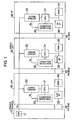
- FIG. 1 schematically shows main sections of a first embodiment of a multi-component system according to the present invention.
- the system includes a power source 10, a reset switch 11, an LAN 20, a serial units 30, a Compact Flash (CF; registered trademark) 40, CPUs 21, 31, and 41; condition detecting units 22, 32, and 42; judge circuits 23, 33, and 43; memories 24, 34, and 44; an LAN Interface (I/F) 25, a serial I/F 35, a CF I/F 45, and a Peripheral Component Interconnect (PCI) Bus 50.
- I/F LAN Interface
- PCI Peripheral Component Interconnect
- the first embodiment includes the power source 10 in addition to the components such as the LAN 20, the serial unit 30, and the CF 40. These components 20, 30, and 40 are mutually connected via the PCI bus 50 to each other.
- the LAN 20 includes the CPU 21, the memory 24 to store therein a program which the CPU 21 executes and data for which the CPU 21 conducts processing, the LAN I/F 25, and the condition detecting unit 22 and the judge circuit 23 which are used to reset the CPU 21.
- the LAN 20 is a component to conduct communication by the LAN I/F 25 with the internet.
- the serial unit 30 includes the CPU 31, the memory 34 to store therein a program which the CPU 31 executes and data for which the CPU 31 conducts processing, the LAN I/F 35, and the condition detecting unit 32 and the judge circuit 33 which are used to reset the CPU 31.
- the serial unit 30 is a component to conduct communication by the LAN I/F 35 with an external device according to, for example, the RSC232C standard.
- the CF 40 includes the CPU 41, the memory 44 to store therein a program which the CPU 41 executes and data for which the CPU 41 conducts processing, the LAN I/F 45, and the condition detecting unit 42 and the judge circuit 43 which are used to reset the CPU 41.
- the CF 40 is a component to conduct communication by the LAN I/F 45 with a recording medium such as a CF card. In this way, the components 20, 30, 40 do not divide the overall processing among them, but respectively execute mutually independent processings.
- the power source 10 includes various operation switches such as a power switch, not shown, and a reset switch 11.
- a high-level reset signal Rs is generated from a reset signal generator or generating unit, not shown, and is fed to respective components (the LAN 20, the serial unit 30, and the CF 40) .
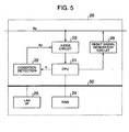
- FIG. 2 shows, in a circuit diagram, specific structure of primary sections of the LAN 20 as one of the components shown in FIG. 1 .
- the sections corresponding to those of FIG. 1 are assigned with the same reference numerals.
- the CPU 21, the RAM 24, and the LAN I/F 25 are connected via the PCI bus 50 to each other.
- the CPU 21 conducts via the PCI bus 50 readout and writing of data from and in the RAM 24 to carry out processing and controls via the PCI bus 50 respective components such as the LAN I/F 25.
- the CPU 21 is connected to the condition detecting unit 22 and the judge circuit 23. Due to the configuration, when the CPU 21 drops to an abnormal condition, the CPU 21 is reset by the reset signal Rs supplied in response to an operation of the reset switch 11 in the power source, which will be described later.
- the configuration is similarly applied to the serial unit 30 and the CF 40 of FIG. 1 .
- These components i.e., the LAN 20, the serial unit 30, and the CF 40 are mutually connected via the PCI bus 50 to each other.
- the condition detecting unit 22 is, for example, a WDT.
- the WDT includes a counter which is reset in response to an interruption signal Ir from the CPU 21.
- the CPU 21 generates the interruption signal Ir at regular intervals.
- the WDT is reset, namely, the WDT resets its value to an initial value to start the counting operation.
- the CPU 21 becomes abnormal, the CPU 21 cannot supply the signal Ir to the WDT, and hence the WDT continues the counting to cause an overflow.
- the WDT generates an abnormality signal Ab and supplies the signal Ab to the judge circuit 23.
- the judge circuit 23 determines that the CPU 21 is in a normal condition and determines not to reset the CPU 21.
- the judge circuit 23 determines that the CPU 21 is in an abnormal condition and determines to reset the CPU 21.
- the reset signal Rs is supplied, the judge circuit resets the CPU 21.
- FIG. 3 shows a concrete example of the judge circuit 23 in a circuit diagram.
- the circuit 23 includes an Set/Reset Multivibrator (S/R MM) 23a and an AND gate 23b.
- S/R MM Set/Reset Multivibrator
- the S/R MM 23a is reset by a terminal edge (falling edge) of a high-level reset signal Rs supplied when the reset switch 11 ( FIG. 1 ) of the power source ( FIG. 1 ) is operated.
- the S/R MM 23a is set by an initial edge of the abnormal signal Ab from the condition detecting unit 22 ( FIG. 1 ). In "set" state, a high-level Q output signal is produced therefrom.
- the Q signal is supplied as a first input to the AND gate 23b, and the reset signal Rs is supplied as a second input thereto.
- the reset signal Rs produced in response to the operation of the reset switch 11 passes through the AND gate 23b.
- the reset signal Rs is fed to the CPU 21 ( FIGS. 1 and 2 ) to reset the CPU 21.
- the CPU 21, 31, and 41 are normally operating in the components, i.e., the LAN 20, the serial unit 30, and CF 40, it is natural that, for example, a control objective device which is not shown normally operates in the system. However, if either one of the CPUs of the components drops to an abnormal condition, the operation of the control objective device is affected by the abnormal condition of the CPU. Hence, the operator can recognize occurrence of an abnormality in either one of the components in the system. If the operator accordingly operates the reset switch 11, the reset signal Rs is generated to be delivered to the LAN 20, the serial unit 30, and CF 40.
- the condition detecting unit 22 detects the abnormal condition and supplies the abnormality signal Ab to the judge circuit 23 as described above.
- the judge circuit 23 judges that the CPU 21 is in the abnormal condition and allows resetting of the CPU 21. If the reset signal Rs is supplied from the power source 10 in this situation, the judge circuit 23 feeds the reset signal Rs to the CPU 21. This resultantly resets the CPU 21.
- the condition detecting units 32 and 42 detect the normal condition of the CPU 31 and 41 and hence do not generate the abnormality signal Ab.
- the judge circuit 33 and 43 judges that the CPUs 31 and 41 are in the normal condition and inhibit resetting thereof. Hence, even if the reset signal Rs is supplied to the CPUs 31 and 41, the CPUs 31 and 41 are not reset and continues processing.
- the CPU of the component in the abnormal condition is reset in response to the operation of the reset switch 11 by the operator, namely, in response to the request from the operator. Therefore, the operator can determine timing to reset the CPU. For example, after conducting a predetermined operation for the control objective device or after securing, if possible, data processed by the pertinent CPU up to this point, the operator may operate the reset switch 11 to reset the CPU of the component in the abnormal condition. If it is possible to secure the processed data, the data can be used when the pertinent CPU is reactivated, and hence the processing up to the point immediately before the occurrence of the abnormality can be effectively used.
- FIG. 4 shows a second embodiment of a multi-component system according to the present invention in a block diagram.
- the embodiment includes reset signal generator circuits 26, 36, and 46.
- the sections corresponding to FIG. 1 are assigned with the same reference numerals, and duplicated description thereof will be avoided.
- the second embodiment of FIG. 4 is implemented by adding the reset signal generator circuits 26, 36, and 46 respectively to the components, i.e., the LAN 20, the serial unit 30, and the CF 40 of the first embodiment shown in FIG. 1 .
- each of the reset signal generator circuits 26, 36, and 46 generates a reset signal Rs' in a format substantially equal to that of the reset signal Rs.
- the CPU of either one of the LAN 20, the serial unit 30, and the CF 40 becomes abnormal, each of the CPUs in a normal condition generates the reset signal Rs'.
- the component in the abnormal condition obtains the signal Rs' via the judge circuit to reset the CPU in the abnormal condition.
- the CPU 21, the RAM 24, and the LAN I/F 25 are coupled via the PCI bus with each other.
- the CPU 21 conducts via the PCI bus 50 readout and writing of data from and in the RAM 24 to carry out processing and controls via the PCI bus 50 respective components such as the LAN I/F 25.
- the CPU 21 is connected to the condition detecting unit 22, the judge circuit 23, and the reset signal generator circuit 26. Due to the configuration, when the CPU 21 drops to an abnormal condition, the CPU 21 is reset by the reset signal Rs supplied in response to an operation of the reset switch 11 in the power source 10 as in the first embodiment.
- the generator circuit 26 is capable of generating a reset signal Rs' in a format substantially equal to that of the reset signal Rs.
- the CPU 21 can communicate via the PCI bus 50 with the other components, i.e., the serial unit 30 and the CF 40.
- the configuration is similarly applied to the serial unit 30 and the CF 40 of FIG. 1 .
- These components i.e., the LAN 20, the serial unit 30, and the CF 40 are mutually connected via the PCI bus 50 to each other.
- the LAN 20 the serial unit 30, and the CF 40, required data is communicated, which will be described later.
- each of the CPUs 21, 31, and 41 of the respective components sends life information indicating that the CPU is in the normal condition via the PCI bus 50 to the other components at regular intervals.
- each CPU in the normal condition continuously recognizes whether or not the CPUs of the other components are in the normal condition.
- the CPU 21 then executes predetermined processing for the serial unit 30. After the processing is finished, the CPU 21 controls the reset generator circuit 26 to generate the reset signal Rs'.
- the signal Rs' is fed to the serial unit 30 and the CF 40.
- the judge circuit 33 has determined to allow the resetting of the CPU 31 and hence sets the AND gate 23b ( FIG. 3 ) to an ON state (that is, the judge circuit 33 is in an ON state). Therefore, at reception of the reset signal Rs' generated by the generator circuit 26 of the LAN 20, the judge circuit 33 is reset on the basis of the signal Rs'.
- the predetermined processing executed by the CPU 21 for the serial unit 30 before the reset generator circuit 26 generates the reset signal Rs' is, for example, as follows. If the CPU 21 detects that the CPU 31 is in the abnormal condition, the CPU 21 executes processing in which a processing program and data are read via the PCI bus 50 from the RAM 34 of the serial unit 30 to store the program and the data in the RAM 24. This secures the result (processed data) of the processing executed by the CPU 31 up to the point immediately before the transition to the abnormal condition so that the CPUs other than the CPU 31 or the CPU 31 after the reactivation thereof can continuously execute processing beginning at a point immediately before the transition to the abnormal condition. Therefore, the result of processing executed by the CPU 31 up to the point immediately before the transition to the abnormal condition will be effectively used. This also makes it possible to control via the PCI bus 50 the serial I/F 35 to continuously execute processing of the serial unit 30.
- the judge circuit 43 judges that the CPU 41 is in the normal condition to inhibit the resetting of the CPU 41. In the CF 40, the judge circuit 43 blocks the reset signal Rs' generated by the generator circuit 26 of the LAN 20, and hence the CPU 41 is not reset.
- the condition detecting unit 22, 32, and 42 respectively detects abnormalities associated with hardware of the CPU 21, 31, and 41.
Landscapes
- Engineering & Computer Science (AREA)
- Theoretical Computer Science (AREA)
- Physics & Mathematics (AREA)
- General Engineering & Computer Science (AREA)
- General Physics & Mathematics (AREA)
- Quality & Reliability (AREA)
- Debugging And Monitoring (AREA)
- Retry When Errors Occur (AREA)
- Developing Agents For Electrophotography (AREA)
- Multi Processors (AREA)
- Hardware Redundancy (AREA)
Claims (5)
- Mehrkomponentensystem, in dem eine Vielzahl von Komponenten (20, 30, 40), die jeweils mindestens eine CPU (21, 31, 41) umfassen, über einen gemeinsamen Bus (50) miteinander verbunden sind, dadurch gekennzeichnet, dass:das Mehrkomponentensystem umfasst:eine erste Rücksetzsignalerzeugungseinheit (11), die ein erstes Rücksetzsignal (Rs) in Erwiderung auf einen Schaltvorgang erzeugt und die das erste Rücksetzsignal an die betreffenden Komponenten über den gemeinsamen Bus liefert, unddass jede Komponente umfasst:eine Zustandsdetektionseinheit (22, 32, 42), die ein durch die CPU (21, 31, 41) in regulären Intervallen gelöschter Überwachungstimer ist und die, wenn der Timer-Löschvorgang unterbrochen ist, detektiert, dass der Zustand der CPU (21, 31, 41) anormal ist, so dass die Zustandsdetektionseinheit so angeordnet, dass sie den normalen Betriebszustand und den anormalen Betriebszustand der CPU (21, 31, 41) der Komponente detektiert, undeine Beurteilungseinheit (23, 33, 43), die die CPU (2.1, 31, 41) der Komponente in Erwiderung auf das erste Rücksetzsignal von der ersten Rücksetzsignalerzeugungseinheit zurücksetzt, falls der anormale Zustand der CPU (21, 31, 41) durch die Zustandsdetektionseinheit detektiert wird, und die das Zurücksetzen der CPU (21, 31, 41) der Komponente in Erwiderung auf das erste Rücksetzsignal (Rs) von der ersten Rücksetzsignalerzeugungseinheit (11) verhindert, falls der normale Zustand der CPU (21, 31, 41) durch die Zustandsdetektionseinheit detektiert wird.
- Mehrkomponentensystem nach Anspruch 1, wobei jede CPU (21, 31, 41) in regulären Intervallen über den gemeinsamen Bus (50) an die anderen Komponenten (20, 30, 40) Existenzinformationen herausgibt, die anzeigen, dass die CPU (21, 31, 41) in einem normalen Zustand ist, wenn die CPU (21, 31, 41) im normalen Zustand ist, und jede CPU (21, 31, 41) die Existenzinformationen von den anderen Komponenten (20, 30, 40) empfängt und dadurch entscheidet, ob jede der CPUs (21, 31, 41) der anderen Komponenten (20, 30, 40) im normalen Zustand ist oder ob nicht, und
jede Komponente (20, 30, 40) eine zweite Rücksetzsignalerzeugungseinheit (26, 36, 46) umfasst, die ein zweites Rücksetzsignal (R's) erzeugt und das zweite Rücksetzsignal (R's) über den gemeinsamen Bus (50) an die Beurteilungseinheiten (23, 33, 43) aller Komponenten im System liefert, wenn die CPU (21, 31, 41) der Komponente (20, 30, 40) entscheidet, dass die CPU (21, 31, 41) einer der anderen Komponenten (20, 30, 40) im anormalen Zustand ist, und
das zweite Rücksetzsignal (R's) dasselbe Format wie das erste Rücksetzsignal (Rs) hat und die Beurteilungseinheit der Komponente (20, 30, 40) das erste Rücksetzsignal (Rs) und das zweite Rücksetzsignal (R's) gleich behandelt. - Mehrkomponentensystem nach Anspruch 3, wobei jede der CPUs (21, 31, 41) der Komponenten (20, 30, 40) im normalen Zustand Daten über den gemeinsamen Bus (50) erhält, die durch die in den anormalen Zustand fallende CPU (21, 31, 41) der Komponente (20, 30, 40) verarbeitet werden, und dann die zweite Rücksetzsignalerzeugungseinheit steuert, um das zweite Rücksetzsignal (R's) zu erzeugen.
- Mehrkomponentensystem nach Anspruch 1, wobei jede Komponente (20, 30, 40) eine LAN-Schnittstelle (25), eine serielle Schnittstelle (35) und eine CF-Schnittstelle (45) zum Kommunizieren mit mindestens einer externen Vorrichtung umfasst.
- Mehrkomponentensystem nach Anspruch 4, wobei jede Komponente (20, 30, 40) eine Prozessdatenspeichereinheit (24, 34, 44) umfasst zum Speichern von über den gemeinsamen Bus (50) erhaltenen Daten, die durch die in einen anormalen Zustand fallende CPU (21, 31, 41) der Komponente verarbeitet werden.
Applications Claiming Priority (1)
| Application Number | Priority Date | Filing Date | Title |
|---|---|---|---|
| JP2007166383A JP5063212B2 (ja) | 2007-06-25 | 2007-06-25 | 複数コンポーネントシステム |
Publications (2)
| Publication Number | Publication Date |
|---|---|
| EP2012217A1 EP2012217A1 (de) | 2009-01-07 |
| EP2012217B1 true EP2012217B1 (de) | 2010-10-20 |
Family
ID=39735218
Family Applications (1)
| Application Number | Title | Priority Date | Filing Date |
|---|---|---|---|
| EP08252138A Active EP2012217B1 (de) | 2007-06-25 | 2008-06-20 | System mit mehreren Komponenten |
Country Status (6)
| Country | Link |
|---|---|
| US (1) | US7861115B2 (de) |
| EP (1) | EP2012217B1 (de) |
| JP (1) | JP5063212B2 (de) |
| CN (1) | CN101334746B (de) |
| AT (1) | ATE485555T1 (de) |
| DE (1) | DE602008003063D1 (de) |
Families Citing this family (7)
| Publication number | Priority date | Publication date | Assignee | Title |
|---|---|---|---|---|
| CN101770268B (zh) * | 2009-12-28 | 2014-06-11 | 中兴通讯股份有限公司 | 智能终端复位方法及装置 |
| EP2600272A2 (de) * | 2010-07-26 | 2013-06-05 | Ki Yong Kim | Steuervorrichtung mit integrierter hackervirus-sicherheit |
| WO2014088559A1 (en) * | 2012-12-04 | 2014-06-12 | Hewlett-Packard Development Company, L.P. | Determining suspected root causes of anomalous network behavior |
| CN103530197B (zh) * | 2013-10-29 | 2017-06-13 | 浙江宇视科技有限公司 | 一种检测及解决Linux系统死锁的方法 |
| US10606702B2 (en) * | 2016-11-17 | 2020-03-31 | Ricoh Company, Ltd. | System, information processing apparatus, and method for rebooting a part corresponding to a cause identified |
| JP6750489B2 (ja) | 2016-12-06 | 2020-09-02 | 株式会社リコー | 電子機器、画像形成装置、制御方法、およびプログラム |
| CN109426321A (zh) * | 2017-08-29 | 2019-03-05 | 深圳市三诺数字科技有限公司 | 一种充电复位电路及电子设备 |
Family Cites Families (24)
| Publication number | Priority date | Publication date | Assignee | Title |
|---|---|---|---|---|
| JPS589488A (ja) * | 1981-07-09 | 1983-01-19 | Pioneer Electronic Corp | 複数の中央演算処理装置を有するシステムの中央演算処理装置の復帰機構 |
| JPS6377244A (ja) * | 1986-09-19 | 1988-04-07 | Nippon Denso Co Ltd | 通信制御装置 |
| US5086505A (en) * | 1989-06-30 | 1992-02-04 | Motorola, Inc. | Selective individual reset apparatus and method |
| JPH04295956A (ja) * | 1991-03-25 | 1992-10-20 | Oki Electric Ind Co Ltd | テレメータ装置 |
| DE69227272T2 (de) * | 1991-04-16 | 1999-03-11 | Nec Corp., Tokio/Tokyo | Multiprozessorssystem |
| JPH0573344A (ja) * | 1991-09-12 | 1993-03-26 | Mitsubishi Electric Corp | 計算機システム |
| JP2729121B2 (ja) * | 1991-11-21 | 1998-03-18 | 甲府日本電気株式会社 | 演算処理装置 |
| JPH05216855A (ja) * | 1992-02-04 | 1993-08-27 | Fujitsu Ltd | マルチcpu制御方式 |
| JP3240679B2 (ja) * | 1992-04-09 | 2001-12-17 | 富士通株式会社 | マルチcpuシステムのリセット方式 |
| JP3684590B2 (ja) * | 1994-04-25 | 2005-08-17 | カシオ計算機株式会社 | リセット制御装置及びリセット制御方法 |
| GB2290891B (en) * | 1994-06-29 | 1999-02-17 | Mitsubishi Electric Corp | Multiprocessor system |
| JPH09319467A (ja) | 1996-05-29 | 1997-12-12 | Hitachi Ltd | バス接続システム |
| JP3266841B2 (ja) | 1997-12-15 | 2002-03-18 | 株式会社日立製作所 | 通信制御装置 |
| US6393590B1 (en) * | 1998-12-22 | 2002-05-21 | Nortel Networks Limited | Method and apparatus for ensuring proper functionality of a shared memory, multiprocessor system |
| JP3266192B2 (ja) * | 1999-01-06 | 2002-03-18 | 日本電気株式会社 | 動作監視方法とそのシステム |
| WO2001016678A1 (en) * | 1999-08-30 | 2001-03-08 | Mitsubishi Denki Kabushiki Kaisha | Programmable controller system and method for resetting programmable controller system |
| US20020152425A1 (en) * | 2001-04-12 | 2002-10-17 | David Chaiken | Distributed restart in a multiple processor system |
| US6912670B2 (en) * | 2002-01-22 | 2005-06-28 | International Business Machines Corporation | Processor internal error handling in an SMP server |
| US7137020B2 (en) * | 2002-05-17 | 2006-11-14 | Sun Microsystems, Inc. | Method and apparatus for disabling defective components in a computer system |
| JP2004005280A (ja) | 2002-05-31 | 2004-01-08 | Omron Corp | プログラマブルコントローラ及びcpuユニット |
| US20050086460A1 (en) * | 2003-10-15 | 2005-04-21 | Chang-Shu Huang | Apparatus and method for wakeup on LAN |
| GB2415799A (en) * | 2004-06-30 | 2006-01-04 | Nec Technologies | Independent processor resetting in a multiprocessor system |
| JP4529767B2 (ja) * | 2005-04-04 | 2010-08-25 | 株式会社日立製作所 | クラスタ構成コンピュータシステム及びその系リセット方法 |
| US8176302B2 (en) * | 2005-10-25 | 2012-05-08 | Nxp B.V. | Data processing arrangement comprising a reset facility |
-
2007
- 2007-06-25 JP JP2007166383A patent/JP5063212B2/ja not_active Expired - Fee Related
-
2008
- 2008-06-20 EP EP08252138A patent/EP2012217B1/de active Active
- 2008-06-20 AT AT08252138T patent/ATE485555T1/de not_active IP Right Cessation
- 2008-06-20 DE DE602008003063T patent/DE602008003063D1/de active Active
- 2008-06-24 CN CN2008101318054A patent/CN101334746B/zh not_active Expired - Fee Related
- 2008-06-24 US US12/215,063 patent/US7861115B2/en not_active Expired - Fee Related
Also Published As
| Publication number | Publication date |
|---|---|
| US20090013221A1 (en) | 2009-01-08 |
| CN101334746A (zh) | 2008-12-31 |
| CN101334746B (zh) | 2011-11-16 |
| DE602008003063D1 (de) | 2010-12-02 |
| ATE485555T1 (de) | 2010-11-15 |
| US7861115B2 (en) | 2010-12-28 |
| EP2012217A1 (de) | 2009-01-07 |
| JP5063212B2 (ja) | 2012-10-31 |
| JP2009003862A (ja) | 2009-01-08 |
Similar Documents
| Publication | Publication Date | Title |
|---|---|---|
| US7861115B2 (en) | Multi-component system | |
| US6845467B1 (en) | System and method of operation of dual redundant controllers | |
| CN101216793A (zh) | 一种多处理器系统故障恢复的方法及装置 | |
| GB2184874A (en) | Diagnostic system | |
| CN104679610A (zh) | 计算机系统的管理方法和装置 | |
| CN114509981B (zh) | 控制器硬件冗余控制方法及系统 | |
| JPS59106056A (ja) | フエイルセイフ式デ−タ処理システム | |
| WO2013018183A1 (ja) | システム制御装置、電力制御方法及び電子システム | |
| US6832331B1 (en) | Fault tolerant mastership system and method | |
| CN102722466A (zh) | 一种3取2或2取2控制系统中的16位多总线电路 | |
| JP2998804B2 (ja) | マルチマイクロプロセッサシステム | |
| EP1988469B1 (de) | Fehlersteuereinrichtung | |
| JP3112068B2 (ja) | 二重化構成装置 | |
| KR100564235B1 (ko) | 알티유(rtu)의 마이크로 콘트롤러 2중화 제어장치와 방법 | |
| JP7786312B2 (ja) | 電子制御装置 | |
| JP7538021B2 (ja) | Plc、及びplcシステム | |
| JPS62226736A (ja) | 二重化システムのデ−タ等値化方法 | |
| JP4983806B2 (ja) | 二重化タイマを用いたシステム監視装置、および監視方法 | |
| EP1290794B1 (de) | Sicherheitssystem | |
| GB2146810A (en) | Achieving redundancy in a distributed process control system | |
| JPH02281343A (ja) | Cpu動作の監視方式 | |
| CN116679223A (zh) | 一种后备电池单元放电测试装置及方法 | |
| JP2510025B2 (ja) | バス制御部監視回路 | |
| KR102301633B1 (ko) | 이중화 구조를 갖는 통신 단말장치 및 그의 신호 중첩 방지 방법 | |
| JP2983221B2 (ja) | メモリ構成設定方法 |
Legal Events
| Date | Code | Title | Description |
|---|---|---|---|
| PUAI | Public reference made under article 153(3) epc to a published international application that has entered the european phase |
Free format text: ORIGINAL CODE: 0009012 |
|
| 17P | Request for examination filed |
Effective date: 20080708 |
|
| AK | Designated contracting states |
Kind code of ref document: A1 Designated state(s): AT BE BG CH CY CZ DE DK EE ES FI FR GB GR HR HU IE IS IT LI LT LU LV MC MT NL NO PL PT RO SE SI SK TR |
|
| AX | Request for extension of the european patent |
Extension state: AL BA MK RS |
|
| 17Q | First examination report despatched |
Effective date: 20090219 |
|
| AKX | Designation fees paid |
Designated state(s): AT BE BG CH CY CZ DE DK EE ES FI FR GB GR HR HU IE IS IT LI LT LU LV MC MT NL NO PL PT RO SE SI SK TR |
|
| AXX | Extension fees paid |
Extension state: MK Payment date: 20080708 Extension state: BA Payment date: 20080708 Extension state: AL Payment date: 20080708 Extension state: RS Payment date: 20080708 |
|
| GRAP | Despatch of communication of intention to grant a patent |
Free format text: ORIGINAL CODE: EPIDOSNIGR1 |
|
| GRAS | Grant fee paid |
Free format text: ORIGINAL CODE: EPIDOSNIGR3 |
|
| GRAA | (expected) grant |
Free format text: ORIGINAL CODE: 0009210 |
|
| AK | Designated contracting states |
Kind code of ref document: B1 Designated state(s): AT BE BG CH CY CZ DE DK EE ES FI FR GB GR HR HU IE IS IT LI LT LU LV MC MT NL NO PL PT RO SE SI SK TR |
|
| AX | Request for extension of the european patent |
Extension state: AL BA MK RS |
|
| REG | Reference to a national code |
Ref country code: GB Ref legal event code: FG4D |
|
| REG | Reference to a national code |
Ref country code: CH Ref legal event code: EP |
|
| REG | Reference to a national code |
Ref country code: IE Ref legal event code: FG4D |
|
| REF | Corresponds to: |
Ref document number: 602008003063 Country of ref document: DE Date of ref document: 20101202 Kind code of ref document: P |
|
| REG | Reference to a national code |
Ref country code: NL Ref legal event code: VDEP Effective date: 20101020 |
|
| LTIE | Lt: invalidation of european patent or patent extension |
Effective date: 20101020 |
|
| PG25 | Lapsed in a contracting state [announced via postgrant information from national office to epo] |
Ref country code: LT Free format text: LAPSE BECAUSE OF FAILURE TO SUBMIT A TRANSLATION OF THE DESCRIPTION OR TO PAY THE FEE WITHIN THE PRESCRIBED TIME-LIMIT Effective date: 20101020 Ref country code: NO Free format text: LAPSE BECAUSE OF FAILURE TO SUBMIT A TRANSLATION OF THE DESCRIPTION OR TO PAY THE FEE WITHIN THE PRESCRIBED TIME-LIMIT Effective date: 20110120 |
|
| PG25 | Lapsed in a contracting state [announced via postgrant information from national office to epo] |
Ref country code: PT Free format text: LAPSE BECAUSE OF FAILURE TO SUBMIT A TRANSLATION OF THE DESCRIPTION OR TO PAY THE FEE WITHIN THE PRESCRIBED TIME-LIMIT Effective date: 20110221 Ref country code: NL Free format text: LAPSE BECAUSE OF FAILURE TO SUBMIT A TRANSLATION OF THE DESCRIPTION OR TO PAY THE FEE WITHIN THE PRESCRIBED TIME-LIMIT Effective date: 20101020 Ref country code: HR Free format text: LAPSE BECAUSE OF FAILURE TO SUBMIT A TRANSLATION OF THE DESCRIPTION OR TO PAY THE FEE WITHIN THE PRESCRIBED TIME-LIMIT Effective date: 20101020 Ref country code: BG Free format text: LAPSE BECAUSE OF FAILURE TO SUBMIT A TRANSLATION OF THE DESCRIPTION OR TO PAY THE FEE WITHIN THE PRESCRIBED TIME-LIMIT Effective date: 20110120 Ref country code: SE Free format text: LAPSE BECAUSE OF FAILURE TO SUBMIT A TRANSLATION OF THE DESCRIPTION OR TO PAY THE FEE WITHIN THE PRESCRIBED TIME-LIMIT Effective date: 20101020 Ref country code: LV Free format text: LAPSE BECAUSE OF FAILURE TO SUBMIT A TRANSLATION OF THE DESCRIPTION OR TO PAY THE FEE WITHIN THE PRESCRIBED TIME-LIMIT Effective date: 20101020 Ref country code: AT Free format text: LAPSE BECAUSE OF FAILURE TO SUBMIT A TRANSLATION OF THE DESCRIPTION OR TO PAY THE FEE WITHIN THE PRESCRIBED TIME-LIMIT Effective date: 20101020 Ref country code: IS Free format text: LAPSE BECAUSE OF FAILURE TO SUBMIT A TRANSLATION OF THE DESCRIPTION OR TO PAY THE FEE WITHIN THE PRESCRIBED TIME-LIMIT Effective date: 20110220 Ref country code: SI Free format text: LAPSE BECAUSE OF FAILURE TO SUBMIT A TRANSLATION OF THE DESCRIPTION OR TO PAY THE FEE WITHIN THE PRESCRIBED TIME-LIMIT Effective date: 20101020 Ref country code: FI Free format text: LAPSE BECAUSE OF FAILURE TO SUBMIT A TRANSLATION OF THE DESCRIPTION OR TO PAY THE FEE WITHIN THE PRESCRIBED TIME-LIMIT Effective date: 20101020 |
|
| PG25 | Lapsed in a contracting state [announced via postgrant information from national office to epo] |
Ref country code: BE Free format text: LAPSE BECAUSE OF FAILURE TO SUBMIT A TRANSLATION OF THE DESCRIPTION OR TO PAY THE FEE WITHIN THE PRESCRIBED TIME-LIMIT Effective date: 20101020 Ref country code: GR Free format text: LAPSE BECAUSE OF FAILURE TO SUBMIT A TRANSLATION OF THE DESCRIPTION OR TO PAY THE FEE WITHIN THE PRESCRIBED TIME-LIMIT Effective date: 20110121 |
|
| PG25 | Lapsed in a contracting state [announced via postgrant information from national office to epo] |
Ref country code: EE Free format text: LAPSE BECAUSE OF FAILURE TO SUBMIT A TRANSLATION OF THE DESCRIPTION OR TO PAY THE FEE WITHIN THE PRESCRIBED TIME-LIMIT Effective date: 20101020 Ref country code: CZ Free format text: LAPSE BECAUSE OF FAILURE TO SUBMIT A TRANSLATION OF THE DESCRIPTION OR TO PAY THE FEE WITHIN THE PRESCRIBED TIME-LIMIT Effective date: 20101020 Ref country code: ES Free format text: LAPSE BECAUSE OF FAILURE TO SUBMIT A TRANSLATION OF THE DESCRIPTION OR TO PAY THE FEE WITHIN THE PRESCRIBED TIME-LIMIT Effective date: 20110131 |
|
| PLBE | No opposition filed within time limit |
Free format text: ORIGINAL CODE: 0009261 |
|
| STAA | Information on the status of an ep patent application or granted ep patent |
Free format text: STATUS: NO OPPOSITION FILED WITHIN TIME LIMIT |
|
| PG25 | Lapsed in a contracting state [announced via postgrant information from national office to epo] |
Ref country code: RO Free format text: LAPSE BECAUSE OF FAILURE TO SUBMIT A TRANSLATION OF THE DESCRIPTION OR TO PAY THE FEE WITHIN THE PRESCRIBED TIME-LIMIT Effective date: 20101020 Ref country code: PL Free format text: LAPSE BECAUSE OF FAILURE TO SUBMIT A TRANSLATION OF THE DESCRIPTION OR TO PAY THE FEE WITHIN THE PRESCRIBED TIME-LIMIT Effective date: 20101020 Ref country code: SK Free format text: LAPSE BECAUSE OF FAILURE TO SUBMIT A TRANSLATION OF THE DESCRIPTION OR TO PAY THE FEE WITHIN THE PRESCRIBED TIME-LIMIT Effective date: 20101020 Ref country code: DK Free format text: LAPSE BECAUSE OF FAILURE TO SUBMIT A TRANSLATION OF THE DESCRIPTION OR TO PAY THE FEE WITHIN THE PRESCRIBED TIME-LIMIT Effective date: 20101020 |
|
| 26N | No opposition filed |
Effective date: 20110721 |
|
| REG | Reference to a national code |
Ref country code: DE Ref legal event code: R097 Ref document number: 602008003063 Country of ref document: DE Effective date: 20110721 |
|
| PG25 | Lapsed in a contracting state [announced via postgrant information from national office to epo] |
Ref country code: MT Free format text: LAPSE BECAUSE OF FAILURE TO SUBMIT A TRANSLATION OF THE DESCRIPTION OR TO PAY THE FEE WITHIN THE PRESCRIBED TIME-LIMIT Effective date: 20101020 Ref country code: IT Free format text: LAPSE BECAUSE OF FAILURE TO SUBMIT A TRANSLATION OF THE DESCRIPTION OR TO PAY THE FEE WITHIN THE PRESCRIBED TIME-LIMIT Effective date: 20101020 |
|
| REG | Reference to a national code |
Ref country code: FR Ref legal event code: ST Effective date: 20120229 |
|
| REG | Reference to a national code |
Ref country code: IE Ref legal event code: MM4A |
|
| PG25 | Lapsed in a contracting state [announced via postgrant information from national office to epo] |
Ref country code: FR Free format text: LAPSE BECAUSE OF NON-PAYMENT OF DUE FEES Effective date: 20110630 Ref country code: IE Free format text: LAPSE BECAUSE OF NON-PAYMENT OF DUE FEES Effective date: 20110620 |
|
| REG | Reference to a national code |
Ref country code: CH Ref legal event code: PL |
|
| REG | Reference to a national code |
Ref country code: CH Ref legal event code: PL |
|
| GBPC | Gb: european patent ceased through non-payment of renewal fee |
Effective date: 20120620 |
|
| PG25 | Lapsed in a contracting state [announced via postgrant information from national office to epo] |
Ref country code: GB Free format text: LAPSE BECAUSE OF NON-PAYMENT OF DUE FEES Effective date: 20120620 Ref country code: MC Free format text: LAPSE BECAUSE OF NON-PAYMENT OF DUE FEES Effective date: 20110630 Ref country code: LI Free format text: LAPSE BECAUSE OF NON-PAYMENT OF DUE FEES Effective date: 20120630 Ref country code: CH Free format text: LAPSE BECAUSE OF NON-PAYMENT OF DUE FEES Effective date: 20120630 |
|
| PG25 | Lapsed in a contracting state [announced via postgrant information from national office to epo] |
Ref country code: LU Free format text: LAPSE BECAUSE OF NON-PAYMENT OF DUE FEES Effective date: 20110620 Ref country code: CY Free format text: LAPSE BECAUSE OF FAILURE TO SUBMIT A TRANSLATION OF THE DESCRIPTION OR TO PAY THE FEE WITHIN THE PRESCRIBED TIME-LIMIT Effective date: 20101020 |
|
| PG25 | Lapsed in a contracting state [announced via postgrant information from national office to epo] |
Ref country code: TR Free format text: LAPSE BECAUSE OF FAILURE TO SUBMIT A TRANSLATION OF THE DESCRIPTION OR TO PAY THE FEE WITHIN THE PRESCRIBED TIME-LIMIT Effective date: 20101020 |
|
| PG25 | Lapsed in a contracting state [announced via postgrant information from national office to epo] |
Ref country code: HU Free format text: LAPSE BECAUSE OF FAILURE TO SUBMIT A TRANSLATION OF THE DESCRIPTION OR TO PAY THE FEE WITHIN THE PRESCRIBED TIME-LIMIT Effective date: 20101020 |
|
| PGFP | Annual fee paid to national office [announced via postgrant information from national office to epo] |
Ref country code: DE Payment date: 20150616 Year of fee payment: 8 |
|
| REG | Reference to a national code |
Ref country code: DE Ref legal event code: R119 Ref document number: 602008003063 Country of ref document: DE |
|
| PG25 | Lapsed in a contracting state [announced via postgrant information from national office to epo] |
Ref country code: DE Free format text: LAPSE BECAUSE OF NON-PAYMENT OF DUE FEES Effective date: 20170103 |