EP2003707B1 - Piezoelektrischer aktuator - Google Patents
Piezoelektrischer aktuator Download PDFInfo
- Publication number
- EP2003707B1 EP2003707B1 EP20070738408 EP07738408A EP2003707B1 EP 2003707 B1 EP2003707 B1 EP 2003707B1 EP 20070738408 EP20070738408 EP 20070738408 EP 07738408 A EP07738408 A EP 07738408A EP 2003707 B1 EP2003707 B1 EP 2003707B1
- Authority
- EP
- European Patent Office
- Prior art keywords
- thick
- film
- conductor
- piezoelectric
- conductors
- Prior art date
- Legal status (The legal status is an assumption and is not a legal conclusion. Google has not performed a legal analysis and makes no representation as to the accuracy of the status listed.)
- Not-in-force
Links
- 239000004020 conductor Substances 0.000 claims abstract description 193
- 239000002184 metal Substances 0.000 claims description 20
- 229910052751 metal Inorganic materials 0.000 claims description 20
- 239000000843 powder Substances 0.000 claims description 14
- 230000002093 peripheral effect Effects 0.000 claims description 13
- 239000011521 glass Substances 0.000 claims description 11
- 239000000919 ceramic Substances 0.000 claims description 2
- 238000006073 displacement reaction Methods 0.000 description 24
- 239000010410 layer Substances 0.000 description 11
- 239000007787 solid Substances 0.000 description 7
- 239000011230 binding agent Substances 0.000 description 5
- 239000000853 adhesive Substances 0.000 description 4
- 230000001070 adhesive effect Effects 0.000 description 4
- 230000015572 biosynthetic process Effects 0.000 description 4
- 229910010293 ceramic material Inorganic materials 0.000 description 4
- 230000010287 polarization Effects 0.000 description 4
- 239000011347 resin Substances 0.000 description 4
- 229920005989 resin Polymers 0.000 description 4
- 238000007650 screen-printing Methods 0.000 description 4
- 229910000679 solder Inorganic materials 0.000 description 4
- 239000002904 solvent Substances 0.000 description 4
- 230000007774 longterm Effects 0.000 description 3
- 238000001465 metallisation Methods 0.000 description 3
- 238000000034 method Methods 0.000 description 3
- 230000003014 reinforcing effect Effects 0.000 description 3
- 239000001856 Ethyl cellulose Substances 0.000 description 2
- ZZSNKZQZMQGXPY-UHFFFAOYSA-N Ethyl cellulose Chemical compound CCOCC1OC(OC)C(OCC)C(OCC)C1OC1C(O)C(O)C(OC)C(CO)O1 ZZSNKZQZMQGXPY-UHFFFAOYSA-N 0.000 description 2
- 229910045601 alloy Inorganic materials 0.000 description 2
- 239000000956 alloy Substances 0.000 description 2
- 230000008602 contraction Effects 0.000 description 2
- 230000002950 deficient Effects 0.000 description 2
- 229920001249 ethyl cellulose Polymers 0.000 description 2
- 235000019325 ethyl cellulose Nutrition 0.000 description 2
- 229910052451 lead zirconate titanate Inorganic materials 0.000 description 2
- 238000007639 printing Methods 0.000 description 2
- 229910001252 Pd alloy Inorganic materials 0.000 description 1
- WUOACPNHFRMFPN-UHFFFAOYSA-N alpha-terpineol Chemical compound CC1=CCC(C(C)(C)O)CC1 WUOACPNHFRMFPN-UHFFFAOYSA-N 0.000 description 1
- 239000005388 borosilicate glass Substances 0.000 description 1
- 238000005219 brazing Methods 0.000 description 1
- 239000001913 cellulose Substances 0.000 description 1
- 229920002678 cellulose Polymers 0.000 description 1
- 230000000052 comparative effect Effects 0.000 description 1
- 238000012669 compression test Methods 0.000 description 1
- 239000012141 concentrate Substances 0.000 description 1
- 229910052802 copper Inorganic materials 0.000 description 1
- SQIFACVGCPWBQZ-UHFFFAOYSA-N delta-terpineol Natural products CC(C)(O)C1CCC(=C)CC1 SQIFACVGCPWBQZ-UHFFFAOYSA-N 0.000 description 1
- 210000003298 dental enamel Anatomy 0.000 description 1
- -1 e.g. Substances 0.000 description 1
- 238000010438 heat treatment Methods 0.000 description 1
- 230000000977 initiatory effect Effects 0.000 description 1
- 238000004898 kneading Methods 0.000 description 1
- HFGPZNIAWCZYJU-UHFFFAOYSA-N lead zirconate titanate Chemical compound [O-2].[O-2].[O-2].[O-2].[O-2].[Ti+4].[Zr+4].[Pb+2] HFGPZNIAWCZYJU-UHFFFAOYSA-N 0.000 description 1
- 239000000463 material Substances 0.000 description 1
- 239000000203 mixture Substances 0.000 description 1
- 239000003960 organic solvent Substances 0.000 description 1
- 239000002356 single layer Substances 0.000 description 1
- 238000005476 soldering Methods 0.000 description 1
- 238000009864 tensile test Methods 0.000 description 1
- 229940116411 terpineol Drugs 0.000 description 1
- 238000003466 welding Methods 0.000 description 1
Images


Classifications
-
- H—ELECTRICITY
- H10—SEMICONDUCTOR DEVICES; ELECTRIC SOLID-STATE DEVICES NOT OTHERWISE PROVIDED FOR
- H10N—ELECTRIC SOLID-STATE DEVICES NOT OTHERWISE PROVIDED FOR
- H10N30/00—Piezoelectric or electrostrictive devices
- H10N30/80—Constructional details
- H10N30/87—Electrodes or interconnections, e.g. leads or terminals
- H10N30/872—Interconnections, e.g. connection electrodes of multilayer piezoelectric or electrostrictive devices
-
- H—ELECTRICITY
- H10—SEMICONDUCTOR DEVICES; ELECTRIC SOLID-STATE DEVICES NOT OTHERWISE PROVIDED FOR
- H10N—ELECTRIC SOLID-STATE DEVICES NOT OTHERWISE PROVIDED FOR
- H10N30/00—Piezoelectric or electrostrictive devices
- H10N30/01—Manufacture or treatment
- H10N30/06—Forming electrodes or interconnections, e.g. leads or terminals
- H10N30/063—Forming interconnections, e.g. connection electrodes of multilayered piezoelectric or electrostrictive parts
Definitions
- the present invention relates to piezoelectric actuators used for the operation of electronic devices, such as magnetic heads, and mechanical elements such as valves. Specifically, the present invention relates to a piezoelectric actuator in which an external conductor is arranged on an outer surface of a piezoelectric component.
- piezoelectric actuators have been used for the operation of various electronic devices and mechanical elements.
- Piezoelectric actuators each include a piezoelectric component and external conductors arranged on outer surfaces of the piezoelectric component and used for applying a voltage to the piezoelectric component.
- piezoelectric component examples include single-layer piezoelectric components each composed of a single piezoelectric component; and multilayer piezoelectric components each composed of a plurality of piezoelectric layers stacked.
- Piezoelectric actuators include piezoelectric components having structures suitable for applications.
- each external conductor is formed by applying a conductive paste to a surface of a piezoelectric component and baking the paste, the conductive paste being formed by kneading a metal powder such as a Ag powder, a glass frit, an organic resin binder, and an organic solvent.
- a piezoelectric component expands and contracts repeatedly during operation.
- the piezoelectric component is repeatedly displaced for long-term operation.
- a stress due to displacement is repeatedly applied to external conductors.
- the long-term operation of the piezoelectric actuator may cause fatigue of the external conductor to form a crack in the external conductor, leading to the fracture of the external conductor.
- the formation of a crack in or fracture of the external conductor impairs the conductivity of the external conductor. As a result, the piezoelectric actuator cannot operate.
- Patent Document 1 discloses a multilayer piezoelectric part 101 shown in Fig. 6 .
- internal electrodes 103a and 103b are formed in a multilayer piezoelectric component 102.
- An external conductor 104 is formed so as to be electrically connected to the internal electrode 103a.
- the external conductor 104 has a structure in which a Ag-wire gauze 104b is embedded in a thick-film conductor 104a mainly composed of a Ag powder.
- the embedment of the wire gauze 104b increases the mechanical strength of the external conductor 104.
- Patent Document 2 discloses a piezoelectric actuator 111 shown in Fig. 7 that is a schematic fragmentary cross-sectional view.
- the piezoelectric actuator 111 includes an external conductor 113 formed on an outer surface of a multilayer piezoelectric component 112.
- the external conductor 113 includes an external electrode 114 which is formed directly on the outer surface of the multilayer piezoelectric component 112 and which is composed of a thick-film conductor; and a meshed metal member 115 attached by brazing or welding to the outer surface of the external electrode 114. That is, the netted metal member 115 is contact-connected to the outer surface of the external electrode 114.
- the formation of a crack in the thick-film conductor 104a applies a stress to the wire gauze 104b integrally embedded in the thick-film conductor 104a, thus possibly causing fracture of the wire gauze 104b in association with the crack formed in the thick-film conductor 104a. That is, the wire gauze 104b has an insufficient reinforcing effect.
- the meshed wire member 115 is contact-connected to the outer surface of the external electrode 114.
- adhesion by such contact connection is not sufficient.
- the repeated displacement of the multilayer piezoelectric component 112 easily results in detachment at the contact connection.
- the metal member 115 is contact-connected to the external electrode 114 located at the outer surface of a portion in which the piezoelectric component is largely displaced, the external electrode 114 is restricted to contact connection.
- a crack is more easily formed at the portion of the external electrode 114 restricted to contact connection.
- EP 1162671 A2 discloses a piezoelectric device comprising a plurality of piezoelectric layers and a plurality of inner electrode layers stacked alternately with each other.
- the outer peripheral side surfaces are formed with a pair of outer electrode layers electrically turned on alternately in such a manner that the inner electrode layers located adjacently to each other through the piezoelectric layers have different polarities.
- Second outer electrode layers configured of a conductive material having a larger breaking elongation than the first outer electrode layers, respectively, are formed on a pair of the first outer electrode layers.
- DE 102005035158 A1 discloses a laminated piezoelectric element having a pair of mesh shaped electrodes joined at the sides of a ceramic laminate through a conductive adhesive.
- US 2002/0043901 A1 discloses a multilayer piezoelectric unit including a plurality of piezoelectric plates of a piezoelectric material and a plurality of internal electrodes of a conductive material arranged in alternate layers.
- the external electrodes are arranged on the side surfaces, respectively, of the multilayer piezoelectric unit and electrically connected to a plurality of the internal electrodes.
- the external electrodes are each configured of an electrode base arranged in contact with a corresponding side surface of the multilayer piezoelectric unit, a tabular metal net conductor arranged on the electrode base, and a plurality of conductive adhesives for partially bonding the electrode base and the tabular metal net conductor.
- DE 10152490 A1 discloses piezoelectric actuators having outer electrodes formed of a base metallization, solder and a reinforcing layer attached to the base metallization by the solder.
- the base metallization is structured by interruptions or recesses.
- a high-reliability piezoelectric actuator including an external conductor formed of a thick-film conductor and arranged on an outer surface of a piezoelectric component, wherein even repeated displacement of the piezoelectric component for long-term operation does not easily cause faulty conduction of the external conductor.
- the first thick-film conductor has a thickness larger than that of the second thick-film conductor.
- detachment at the bonding portion of the first thick-film conductor and the second thick-film conductor is further suppressed.
- each of the thick-film conductors is formed by baking a conductive paste containing a metal powder, a glass frit, and an organic vehicle, and the total content of the metal powder and the glass frit is in the range of 85 to 95 percent by weight relative to the conductive paste.
- adhesion strength between the piezoelectric component and the first thick-film conductor and between the conductive reinforcer and the second thick-film conductor is more effectively increased.
- faulty conduction of the external conductor is still further suppressed.
- the plurality of second thick-film conductors are arranged to have a frame-like shape in plan.
- the piezoelectric actuator has four strip-shaped thick-film conductors as the plurality of second thick-film conductors, and the four strip-shaped thick-film conductors are arranged to have a rectangular frame-like shape. In this case, adhesion strength between the second thick-film conductors and the first thick-film conductor and between the second thick-film conductors and the conductive reinforcer are still further increased.
- the first and second thick-film conductors are arranged in such a manner that the peripheral line of the second thick-film conductor is located inside the peripheral line of the first thick-film conductor, and a step is formed inside the peripheral line of the external conductor.
- the presence of the step disperses a stress applied to the external conductor at the peripheral line of the external conductor, thereby more surely suppressing a crack in and fracture of the external electrode.
- the external conductor is formed on the at least one main surface of the piezoelectric component.
- the external conductor includes the thick-film conductor and the conductive reinforcer.
- the thick-film conductor is provided with the planar-shaped first thick-film conductor and the plurality of second thick-film conductors which are formed on part of the first thick-film conductor and which are in surface-contact with the first thick-film conductor.
- the conductive reinforcer is attached to the outer surfaces of the second thick-film conductors so as not to be in direct contact with the first thick-film conductor. Thus, sufficiently high adhesion strength is provided between the first thick-film conductor and the second thick-film conductor.
- the conductive reinforcer is not directly attached to the first thick-film conductor.
- the conductive reinforcer is not easily affected by the crack.
- the conductive reinforcer is not easily broken. That is, the conductive reinforcer ensures the continuity of the external conductor in the planar direction.
- detachment at the bonding portions between the first and second thick-film conductors and between the thick-film conductor and the conductive reinforcer is suppressed.
- faulty conduction of the external conductor is suppressed in the piezoelectric actuator, thereby effectively improving the reliability of the piezoelectric actuator.
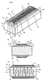
- Figs. 1(a), 1(b), and 1(c) are a perspective view showing the appearance, a cross-sectional view, and a longitudinal sectional view, respectively, of a piezoelectric actuator according to a first embodiment of the present invention.
- a piezoelectric actuator 1 includes a multilayer piezoelectric component 2 that is in the form of a rectangular parallelepiped.
- the multilayer piezoelectric component 2 has a top face 2a, a bottom face 2b, and side faces 2c and 2d.
- the direction in which the side face 2c is connected to the side face 2d is the longitudinal direction of the piezoelectric component 2.
- a plurality of first internal electrodes 3 and a plurality of second internal electrodes 4 are formed in the piezoelectric component 2 so as to extend in a direction parallel to the side faces 2c and 2d, i.e., so as to extend vertically.
- the first internal electrodes 3 and the second internal electrodes 4 are alternately arranged in the direction in which the side face 2c is connected to the side face 2d.
- the plurality of first internal electrodes 3 extend to the top face 2a and do not reach the bottom face 2b.
- the plurality of second internal electrodes 4 extend to the bottom face 2b and do not reach the top face 2a.
- the first and second internal electrodes 3 and 4 are arranged so as to overlap with each other at an intermediate position in height of the piezoelectric component 2.
- the piezoelectric component 2 may be composed of an appropriate piezoelectric ceramic material such as a lead zirconate titanate ceramic material.
- the internal electrodes 3 and 4 are each composed of an appropriate metal such as Ag or an alloy such as Ag-Pd.
- the internal electrodes 3 and 4 may be formed by, for example, a thin-film-forming method or by applying a conductive paste on a green sheet of a piezoelectric ceramic material by printing.
- a first external conductor 5 is arranged on the top face 2a.
- a second external conductor 6 is arranged on the bottom face 2b.
- the first external conductor 5 includes a thick-film conductor and a conductive reinforcer 9.
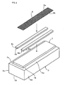
- the thick-film conductor includes a first thick-film conductor 7 formed directly on the top face 2a of the piezoelectric component 2; and a plurality of second thick-film conductors 8a and 8b formed on part of an outer surface of the first thick-film conductor 7, the second thick-film conductors 8a and 8b being in surface-contact with the outer surface.
- the plurality of second thick-film conductor segments 8a and 8b each have a strip shape in plan as shown in Fig. 2 that is an exploded perspective view.
- the second thick-film conductors 8a and 8b are arranged parallel to each other at predetermined intervals.
- the longitudinal length of each of the second thick-film conductors 8a and 8b is smaller than that of the first thick-film conductor 7 having a rectangular shape in plan.
- Figs. 1(a) and 1(c) clearly show that an end of each of the second thick-film conductors 8a and 8b in the longitudinal direction is arranged inside the corresponding end of the first thick-film conductor 7 in the longitudinal direction. As a result, a step represented by Arrow A is formed.
- the conductive reinforcer 9 is formed of a net member composed of a metal such as Ag.
- the conductive reinforcer 9 has a rectangular shape in plan. Outer sides 9a and 9b of the conductive reinforcer 9 in the width direction are arranged inside the outer sides of the second thick-film conductors 8a and 8b. As a result, a step C represented by Arrow C is formed on the external conductor 5.
- the first thick-film conductor 7 and the second thick-film conductors 8a and 8b are formed by applying a conductive paste containing a metal powder, a glass frit, an organic vehicle, and a solvent and then baking the paste.
- the thick-film conductors 7, 8a, and 8b may be formed by another method.
- Examples of the metal powder usable include appropriate metal powders such as a Ag powder and Ag-Pd alloy powders.
- the glass frit usable include appropriate glass frits such as borosilicate glass frits.
- the organic resin binder usable include organic resin binders, such as cellulose binders, e.g., ethyl cellulose, for use in appropriate conductive pastes.
- the first thick-film conductor 7 has a thickness larger than the thickness of each of the second thick-film conductors 8a and 8b, thereby increasing adhesion between the first thick-film conductor 7 and the piezoelectric component 2 and between the first thick-film conductor 7 and the second thick-film conductors 8a and 8b and thus more effectively suppressing faulty conduction.
- the composition of the conductive paste is not particularly limited.
- the conductive paste in which the total content of the metal powder and the glass frit is 85 to 95 percent by weight relative to the overall conductive paste containing the solvent is used.
- a total content of 85 percent by weight or more effectively increases adhesion between the resulting thick-film conductors, between the thick-film conductors and the conductive reinforcer, and between the first thick-film conductor and the piezoelectric component 2.
- a total content exceeding 95 percent by weight causes difficulty in forming the paste due to an excessively low content of the solvent.
- the steps A and B are formed. Even when the multilayer piezoelectric component 2 expands and contracts repeatedly during operation, a stress due to expansion and contraction does not easily concentrate on a portion of the outer ends of the external conductor 5. That is, the external conductor 5 has the steps A and B. Hence, a stress applied is dispersed at the periphery of the external conductor 5. As a result, the formation of a crack in and detachment of the external conductor 5 are further suppressed.
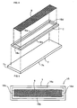
- Figs. 3(a), 3(b), and 3(c) are a perspective view showing the appearance, a cross-sectional view, and a longitudinal sectional view, respectively, of a piezoelectric actuator according to a second embodiment of the present invention.
- a piezoelectric actuator 11 according to the second embodiment includes the multilayer piezoelectric component 2 in the same way as in the piezoelectric actuator 1 according to the first embodiment.
- a first external conductor 15 is formed on the top face 2a of the piezoelectric component 2.
- a second external conductor 16 is formed on the bottom face 2b.
- the difference between the piezoelectric actuator 11 according to the second embodiment and the piezoelectric actuator 1 according to the first embodiment is that in the external conductors 15 and 16, a plurality of second thick-film conductors 18a to 18d are arranged so as to have a rectangular frame-like shape.
- the piezoelectric actuator 11 according to the second embodiment has the same structure as the piezoelectric actuator 1 according to the first embodiment.
- Like references designate identical elements, and description described in the first embodiment is also used.
- the four strip-shaped second thick-film conductors 18a to 18d are formed on part of the first thick-film conductor 7 so as to be in surface-contact with the first thick-film conductor 7.
- the pair of strip-shaped second thick-film conductors 18a and 18b that extend in parallel with each other extend in the longitudinal direction of the piezoelectric component 2.
- the pair of second thick-film conductors 18c and 18d that extend in the direction orthogonal to the thick-film conductors 18a and 18b are arranged so as to connect ends of the thick-film conductors 18a and 18b in the longitudinal direction to form a rectangular frame-like shape.
- the conductive reinforcer 9 is attached to the second thick-film conductors 18a to 18d in such a manner that the peripheral line of the conductive reinforcer 9 is located on a position represented by Broken line C in Fig. 4 and that the conductive reinforcer 9 is in surface-contact with the second thick-film conductors 18a to 18d.
- Fig. 5 is a plan view of the external conductor 15.
- the plurality of second thick-film conductors 18a to 18d are arranged to have a frame-like shape in plan.
- the plurality of second thick-film conductors 18a to 18d are arranged to have the rectangular frame-like shape.
- the second thick-film conductors 18a to 18d are not easily deformed by the stress. Therefore, even when a stress resulting from the displacement of the multilayer piezoelectric component 2 is applied to the external conductor 15, a partial crack in and detachment of the first external conductor 15 is further suppressed.
- the second thick-film conductors 18a to 18d are arranged to have the rectangular frame-like shape.
- the second thick-film conductors 18a to 18d may be arranged to have another polygonal frame-like shape other than a rectangle or a circular shape.
- the steps A and B are formed.
- the present invention does not necessarily require the steps A and B. That is, the peripheral line of the second thick-film conductor need not necessarily be located inside the peripheral line of the first thick-film conductor. Similarly, the peripheral line of the conductive reinforcer need not necessarily be located inside the peripheral line of the second thick-film conductor.
- the formation of the steps A and B as in the first and second equivalents more effectively prevents a partial crack in and detachment of the external conductor when a stress due to the displacement of the piezoelectric component 2 is applied.
- the plurality of second thick-film conductors 18a to 18d are integrally formed to have the rectangular frame-like shape in plan.
- the second thick-film conductors 18a to 18d may be integrally formed by screen printing with a conductive paste. That is, each of the plurality of second thick-film conductors need not necessarily be separately formed.
- the second thick-film conductors may be integrally formed.
- the piezoelectric actuator 11 according to the second embodiment was produced by the following procedure.
- a Ag powder, a B 2 O 3 -SiO 2 -CaO-based glass frit, ethyl cellulose as an organic resin binder, and terpineol as an solvent were mixed with a three-roll mill to form a conductive paste.
- the total solid content of Ag and the glass frit relative to the conductive paste was set at 80 percent by weight.
- a multilayer piezoelectric component 2 having a size of 7 mm ⁇ 7 mm ⁇ 35 mm and composed of a PZT ceramic material was prepared.
- the conductive paste was applied by screen printing to the top face 2a and the bottom face 2b of the multilayer piezoelectric component 2 so as to have an outer size of 5 mm ⁇ 31 mm after baking.
- the same conductive paste was applied by screen printing so as to form the second thick-film conductors 18a to 18d having a rectangular frame-like shape.
- the conductive paste was applied by printing in such a manner that the outer size of the rectangular frame-like shape in plan was 4.5 mm ⁇ 30 mm and that the width of a frame portion was 1.5 mm after baking.
- a Ag gauze as the conductive reinforcer 9 having a rectangular shape with a size of 4 mm ⁇ 28 mm in plan, a wire-diameter of 150 ⁇ m, and a mesh opening of 40 was placed.
- the conductive paste to be formed into the second thick-film conductor was dried by heating.
- the conductive paste to be formed into each of the first and second thick-film conductors was baked to form the external conductors 15 and 16.
- a piezoelectric actuator as a known example was prepared in the same way as above, except that the external conductor was formed by applying the conductive paste for forming the first thick-film conductor by screen printing, embedding the Ag gauze, and baking the conductive paste.
- the piezoelectric actuator as the known example did not have the second thick-film conductor.
- Cu leads each having a wire diameter of 250 ⁇ m and covered with enamel were bonded to the piezoelectric actuators according to the second embodiment and known example by soldering with Sn-3Ag-0.5Cu solder at a temperature of 350°C. Furthermore, to impart piezoelectric characteristics, the multilayer piezoelectric components 2 were subjected to polarization treatment.
- Each of the resulting piezoelectric actuators according to the second embodiment and known example for comparison was driven 100 times by passing a current with a frequency of 30 Hz at a voltage of 200 V. Then the amount of displacement after polarization treatment was measured. The average value of the amount of displacement obtained by 100 operations was defined as the amount of initial displacement.
- the piezoelectric actuator having an amount of initial displacement of 40 ⁇ m or more was defined as a non-defective actuator.
- the number N of samples was set at five in each of the second embodiment and the comparative example.
- a current applying test was repeated at a voltage of 200 V and a frequency of 200 Hz.
- the number of driving cycles when the actuator was destroyed was determined.
- each piezoelectric actuator was held by metal plates.
- the amount of displacement was measured in the same way as in the amount of initial displacement.
- the sample having an amount of displacement of 40 ⁇ m or more after the driving test was defined as a non-defective sample.
- the number N of samples was set at three.
- Table 1 shows the results. [Table 1] Initial property Number of driving cycle After driving test Amount of displacement ( ⁇ m) Capacitance ( ⁇ F) (cycle) Amount of displacement ( ⁇ m) Capacitance ( ⁇ F) Known example 47.3 4.1 3.6 ⁇ 10 8 35.4 3.03 Embodiment 47.1 4.09 5.0 ⁇ 10 8 45.5 3.96
- the piezoelectric actuator according to the known example there were no problem of the amount of initial displacement and capacitance.
- the actuator was stopped at the number of driving cycles of less than 5.0 x 10 8 , in some cases. After the driving test, the amount of displacement and capacitance were reduced. Observation of the appearance of the sample after the driving test showed that the external conductor was cracked along a crack formed in the external conductor during polarization treatment and that the embedded Ag gauze was broken.
- the broken Ag gauze or the like causes discharge, thereby possibly resulting in the termination of operation and the reduction in the amount of displacement.
- the amount of displacement and capacitance were sufficient even after the driving test. Observation of the appearance after the driving test showed that the thick-film conductor was cracked but that the Ag gauze was not broken because the Ag gauze was not markedly restricted to the thick-film conductor. Therefore, it was found that the conduction of the external conductor in the planar direction was sufficiently ensured.
- conductive paste Five types were prepared by changing the solid content within 75.0 to 95.0 percent by weight as shown in Table 2, the solid content being defined as the total content of the Ag powder and the glass frit in the conductive paste prepared in the first experimental example. Piezoelectric actuators were produced with the five types of conductive paste as in the first experimental example.
- Table 2 clearly shows that Samples 3 to 5 each having a solid content of the conductive paste of 85 to 95 percent by weight have high adhesion strength compared with other Samples. This may be because Samples 1 and 2 each having a solid content of 80 percent by weight or less each have a large amount of shrinkage when the conductive pastes were dried and baked, thereby reducing denseness of each thick-film conductor. At a solid content exceeding 95 percent by weight, a conductive paste could not be formed.
- the metal gauze composed of Ag or the like is used.
- a conductive reinforcing plate in which many holes are formed in a thin metal plate may be used. That is, the shape of the conductive reinforcer is not particularly limited.
- the metal constituting the conductive reinforcer is not limited to Ag.
- a metal such as Cu or Al or any of various alloys may be used.
Landscapes
- Engineering & Computer Science (AREA)
- Manufacturing & Machinery (AREA)
- General Electrical Machinery Utilizing Piezoelectricity, Electrostriction Or Magnetostriction (AREA)
- Electrically Driven Valve-Operating Means (AREA)
Claims (5)
- Ein piezoelektrisches Betätigungselement (1; 11), das folgende Merkmale aufweist:eine piezoelektrische Komponente (2) mit einer piezoelektrischen Keramikschicht; undeinen externen Leiter (5, 6; 15, 16), der auf zumindest einer Hauptoberfläche der piezoelektrischen Komponente (2) angeordnet ist,wobei der externe Leiter (5, 6; 15, 16) einen Dickfilmleiter und einen leitfähigen Verstärker (9) aufweist,dadurch gekennzeichnet, dassder Dickfilmleiter mit einem planarförmigen ersten Dickfilmleiter (7) versehen ist, der auf zumindest einer Hauptoberfläche der piezoelektrischen Komponente (2) angeordnet ist und mit einer Mehrzahl von zweiten Dickfilmleitern (8a, 8b; 18a - 18d) versehen ist, die auf einem Teil des ersten Dickfilmleiters (7) angeordnet sind, wobei die zweiten Dickfilmleiter (8a, 8b; 18a - 18d) in Oberflächenkontakt mit dem ersten Dickfilmleiter (7) sind, undder leitfähige Verstärker (9) an einer äußeren Oberfläche der zweiten Dickfilmleiter (8a, 8b; 18a - 18d) befestigt ist, um nicht in direktem Kontakt mit dem ersten Dickfilmleiter (7) zu sein,wobei jeder der Dickfilmleiter gebildet wird durch Backen einer leitfähigen Paste, die ein Metallpulver, eine Glasfritte und ein organisches Trägermittel enthält.
- Das piezoelektrische Betätigungselement (1; 11) gemäß Anspruch 1, bei dem der erste Dickfilmleiter (7) eine Dicke aufweist, die größer ist als diejenige des zweiten Dickfilmleiters (8a, 8b; 18a - 18d).
- Das piezoelektrische Betätigungselement gemäß einem der Ansprüche 1 oder 2, bei dem die Mehrzahl von zweiten Dickfilmleitern angeordnet ist, um in der Draufsicht eine rahmenartige Form zu haben.
- Das piezoelektrische Betätigungselement (11) gemäß Anspruch 1, bei dem das piezoelektrische Betätigungselement (11) vier streifenförmige Dickfilmleiter als die Mehrzahl von zweiten Dickfilmleitern (18a - 18d) aufweist, und die vier streifenförmigen Dickfilmleiter angeordnet sind, um eine rechteckige rahmenartige Form zu haben.
- Das piezoelektrische Betätigungselement (1, 11) gemäß einem der Ansprüche 1 bis 3, bei dem der erste und der zweite Dickfilmleiter (7, 8a, 8b; 18a - 18d) auf solch eine Weise angeordnet sind, dass die Umfangslinie des zweiten Dickfilmleiters (8a, 8b; 18a - 18d) innerhalb der Umfangslinie des ersten Dickfilmleiters (7) angeordnet ist, und eine Stufe (A, B) innerhalb der Umfangslinie des äußeren Leiters (5, 6; 15, 16) gebildet wird.
Applications Claiming Priority (2)
| Application Number | Priority Date | Filing Date | Title |
|---|---|---|---|
| JP2006097575 | 2006-03-31 | ||
| PCT/JP2007/054936 WO2007114002A1 (ja) | 2006-03-31 | 2007-03-13 | 圧電アクチュエータ |
Publications (3)
| Publication Number | Publication Date |
|---|---|
| EP2003707A1 EP2003707A1 (de) | 2008-12-17 |
| EP2003707A4 EP2003707A4 (de) | 2010-10-13 |
| EP2003707B1 true EP2003707B1 (de) | 2012-03-14 |
Family
ID=38563274
Family Applications (1)
| Application Number | Title | Priority Date | Filing Date |
|---|---|---|---|
| EP20070738408 Not-in-force EP2003707B1 (de) | 2006-03-31 | 2007-03-13 | Piezoelektrischer aktuator |
Country Status (6)
| Country | Link |
|---|---|
| US (1) | US7777398B2 (de) |
| EP (1) | EP2003707B1 (de) |
| JP (1) | JP4154538B2 (de) |
| CN (1) | CN101405882B (de) |
| AT (1) | ATE549750T1 (de) |
| WO (1) | WO2007114002A1 (de) |
Cited By (1)
| Publication number | Priority date | Publication date | Assignee | Title |
|---|---|---|---|---|
| DE102012105517A1 (de) * | 2012-06-25 | 2014-01-02 | Epcos Ag | Vielschichtbauelement mit einer Außenkontaktierung und Verfahren zur Herstellung eines Vielschichtbauelements mit einer Außenkontaktierung |
Families Citing this family (12)
| Publication number | Priority date | Publication date | Assignee | Title |
|---|---|---|---|---|
| JP4929875B2 (ja) * | 2006-06-30 | 2012-05-09 | 株式会社デンソー | 積層型圧電素子 |
| CN101911325B (zh) * | 2007-12-26 | 2013-05-15 | 京瓷株式会社 | 层叠型压电元件、利用该元件的喷射装置及燃料喷射系统 |
| EP2259352B1 (de) * | 2008-04-11 | 2012-08-29 | Murata Manufacturing Co. Ltd. | Beschichteter piezoelektrischer aktuator |
| JPWO2009130863A1 (ja) * | 2008-04-21 | 2011-08-11 | 株式会社村田製作所 | 積層型圧電アクチュエータ |
| DE102008062021A1 (de) * | 2008-08-18 | 2010-03-04 | Epcos Ag | Piezoaktor in Vielschichtbauweise |
| JP5385400B2 (ja) * | 2009-10-23 | 2014-01-08 | 株式会社村田製作所 | 電気機械変換素子及びアクチュエータ |
| DE102010063385A1 (de) * | 2010-12-17 | 2012-06-21 | Robert Bosch Gmbh | Piezoaktor |
| US8450910B2 (en) * | 2011-01-14 | 2013-05-28 | General Electric Company | Ultrasound transducer element and method for providing an ultrasound transducer element |
| WO2012115230A1 (ja) * | 2011-02-24 | 2012-08-30 | 京セラ株式会社 | 積層型圧電素子およびこれを備えた噴射装置ならびに燃料噴射システム |
| DE102012109250B4 (de) * | 2012-09-28 | 2020-07-16 | Tdk Electronics Ag | Elektrisches Bauelement und Verfahren zur Herstellung einer Kontaktierung eines Elektrischen Bauelements |
| CN105374929B (zh) * | 2015-11-20 | 2018-10-30 | 中国科学院上海硅酸盐研究所 | 一种织构化无铅压电陶瓷多层驱动器及其制备方法 |
| DE112019004743T5 (de) * | 2018-09-21 | 2021-06-02 | Murata Manufacturing Co., Ltd. | Piezoelektrisches Bauelement |
Family Cites Families (19)
| Publication number | Priority date | Publication date | Assignee | Title |
|---|---|---|---|---|
| DE4201937C2 (de) * | 1991-01-25 | 1997-05-22 | Murata Manufacturing Co | Piezoelektrisches laminiertes Stellglied |
| DE19646676C1 (de) * | 1996-11-12 | 1998-04-23 | Siemens Ag | Piezoaktor mit neuartiger Kontaktierung und Herstellverfahren |
| DE19928190A1 (de) | 1999-06-19 | 2001-01-11 | Bosch Gmbh Robert | Piezoaktor |
| US6396193B1 (en) * | 1999-10-01 | 2002-05-28 | Ngk Insulators, Ltd. | Piezoelectric/electrostrictive device having mutually opposing thin plate portions |
| JP4158338B2 (ja) * | 2000-06-06 | 2008-10-01 | 株式会社デンソー | インジェクタ用圧電体素子 |
| DE10152490A1 (de) * | 2000-11-06 | 2002-05-08 | Ceramtec Ag | Außenelektroden an piezokeramischen Vielschichtaktoren |
| JP3964184B2 (ja) * | 2000-12-28 | 2007-08-22 | 株式会社デンソー | 積層型圧電アクチュエータ |
| US6548943B2 (en) * | 2001-04-12 | 2003-04-15 | Nokia Mobile Phones Ltd. | Method of producing thin-film bulk acoustic wave devices |
| JP3815285B2 (ja) * | 2001-10-09 | 2006-08-30 | ブラザー工業株式会社 | インクジェットヘッド |
| JP4422973B2 (ja) * | 2002-08-27 | 2010-03-03 | 京セラ株式会社 | 積層圧電体、アクチュエータ及び印刷ヘッド |
| JP4208234B2 (ja) | 2003-03-24 | 2009-01-14 | 株式会社ノリタケカンパニーリミテド | 圧電セラミック材用導体ペースト及びその利用 |
| JP2005183478A (ja) * | 2003-12-16 | 2005-07-07 | Ibiden Co Ltd | 積層型圧電素子 |
| WO2005064700A1 (ja) | 2003-12-26 | 2005-07-14 | Murata Manufacturing Co., Ltd | 厚膜電極、及び積層セラミック電子部品 |
| JP4355665B2 (ja) | 2004-04-09 | 2009-11-04 | Tdk株式会社 | 圧電磁器および圧電素子 |
| JP2006041279A (ja) * | 2004-07-28 | 2006-02-09 | Denso Corp | 積層型圧電体素子及びその製造方法 |
| US7249817B2 (en) * | 2005-03-17 | 2007-07-31 | Hewlett-Packard Development Company, L.P. | Printer having image dividing modes |
| JP2006303044A (ja) * | 2005-04-18 | 2006-11-02 | Denso Corp | 積層型圧電体素子 |
| US7998362B2 (en) * | 2005-08-23 | 2011-08-16 | Canon Kabushiki Kaisha | Piezoelectric substance, piezoelectric element, liquid discharge head using piezoelectric element, liquid discharge apparatus, and production method of piezoelectric element |
| JP2007173320A (ja) * | 2005-12-19 | 2007-07-05 | Denso Corp | 積層型圧電素子及びその製造方法 |
-
2007
- 2007-03-13 JP JP2007534958A patent/JP4154538B2/ja not_active Expired - Fee Related
- 2007-03-13 CN CN2007800101439A patent/CN101405882B/zh not_active Expired - Fee Related
- 2007-03-13 EP EP20070738408 patent/EP2003707B1/de not_active Not-in-force
- 2007-03-13 AT AT07738408T patent/ATE549750T1/de active
- 2007-03-13 WO PCT/JP2007/054936 patent/WO2007114002A1/ja not_active Ceased
- 2007-09-19 US US11/857,599 patent/US7777398B2/en active Active
Cited By (2)
| Publication number | Priority date | Publication date | Assignee | Title |
|---|---|---|---|---|
| DE102012105517A1 (de) * | 2012-06-25 | 2014-01-02 | Epcos Ag | Vielschichtbauelement mit einer Außenkontaktierung und Verfahren zur Herstellung eines Vielschichtbauelements mit einer Außenkontaktierung |
| DE102012105517B4 (de) * | 2012-06-25 | 2020-06-18 | Tdk Electronics Ag | Vielschichtbauelement mit einer Außenkontaktierung und Verfahren zur Herstellung eines Vielschichtbauelements mit einer Außenkontaktierung |
Also Published As
| Publication number | Publication date |
|---|---|
| EP2003707A4 (de) | 2010-10-13 |
| ATE549750T1 (de) | 2012-03-15 |
| CN101405882A (zh) | 2009-04-08 |
| CN101405882B (zh) | 2011-06-15 |
| JPWO2007114002A1 (ja) | 2009-08-13 |
| EP2003707A1 (de) | 2008-12-17 |
| WO2007114002A1 (ja) | 2007-10-11 |
| JP4154538B2 (ja) | 2008-09-24 |
| US7777398B2 (en) | 2010-08-17 |
| US20080007144A1 (en) | 2008-01-10 |
Similar Documents
| Publication | Publication Date | Title |
|---|---|---|
| EP2003707B1 (de) | Piezoelektrischer aktuator | |
| EP1701391B1 (de) | Mehrschichtiges piezoelektrisches Bauelement mit Dickfilm-Aussenelektrode | |
| US7944128B2 (en) | Electronic component | |
| US7518295B2 (en) | Multilayer piezoelectric element | |
| CA2271281A1 (en) | Piezo electric actuator with a new type of contacting and a method for the production thereof | |
| KR102127803B1 (ko) | 인터포저 및 이 인터포저를 포함하는 전자 부품 | |
| EP0584842A2 (de) | Geschichtete Keramikanordnung und Verfahren zur deren Herstellung | |
| KR20190121156A (ko) | 전자 부품 | |
| KR20050061442A (ko) | 다층의 압전세라믹 액추에이터 상에 제공된 외부 전극 | |
| KR20190121211A (ko) | 전자 부품 | |
| EP2259353A1 (de) | Mehrschichtiger piezoelektrischer aktuator | |
| JP4670260B2 (ja) | 積層型電子部品 | |
| JP2001210886A (ja) | 積層型圧電アクチュエータ | |
| US7279217B2 (en) | Multilayer ceramic device, method for manufacturing the same, and ceramic device | |
| JP5087822B2 (ja) | 圧電素子 | |
| JP2000294843A (ja) | 圧電素子及び積層型圧電アクチュエータ | |
| JP6424460B2 (ja) | 積層セラミックコンデンサ及びその製造方法 | |
| KR20210030781A (ko) | 적층형 커패시터 및 그 실장 기판 | |
| KR102118494B1 (ko) | 전자 부품 | |
| JP4283751B2 (ja) | 電子部品の製造方法及び電子部品 | |
| JP4737948B2 (ja) | 積層型圧電素子の製法 | |
| JPH0496286A (ja) | 積層型圧電体の製造方法 | |
| JP3227896B2 (ja) | 積層型圧電体 | |
| JPH04188808A (ja) | 表面実装形チップ部品 | |
| JP2003347614A (ja) | 積層型圧電アクチュエータ |
Legal Events
| Date | Code | Title | Description |
|---|---|---|---|
| PUAI | Public reference made under article 153(3) epc to a published international application that has entered the european phase |
Free format text: ORIGINAL CODE: 0009012 |
|
| 17P | Request for examination filed |
Effective date: 20070828 |
|
| RBV | Designated contracting states (corrected) |
Designated state(s): AT BE BG CH CY CZ DE DK EE ES FI FR GB GR HU IE IS IT LI LT LU LV MC MT NL PL PT RO SE SI SK TR |
|
| A4 | Supplementary search report drawn up and despatched |
Effective date: 20100910 |
|
| RIC1 | Information provided on ipc code assigned before grant |
Ipc: H01L 41/047 20060101ALI20100906BHEP Ipc: H01L 41/083 20060101AFI20071210BHEP |
|
| 17Q | First examination report despatched |
Effective date: 20110510 |
|
| RIC1 | Information provided on ipc code assigned before grant |
Ipc: H01L 41/083 20060101AFI20110817BHEP Ipc: H01L 41/047 20060101ALI20110817BHEP |
|
| GRAP | Despatch of communication of intention to grant a patent |
Free format text: ORIGINAL CODE: EPIDOSNIGR1 |
|
| DAX | Request for extension of the european patent (deleted) | ||
| GRAS | Grant fee paid |
Free format text: ORIGINAL CODE: EPIDOSNIGR3 |
|
| GRAA | (expected) grant |
Free format text: ORIGINAL CODE: 0009210 |
|
| AK | Designated contracting states |
Kind code of ref document: B1 Designated state(s): AT BE BG CH CY CZ DE DK EE ES FI FR GB GR HU IE IS IT LI LT LU LV MC MT NL PL PT RO SE SI SK TR |
|
| REG | Reference to a national code |
Ref country code: GB Ref legal event code: FG4D |
|
| REG | Reference to a national code |
Ref country code: AT Ref legal event code: REF Ref document number: 549750 Country of ref document: AT Kind code of ref document: T Effective date: 20120315 Ref country code: CH Ref legal event code: EP |
|
| REG | Reference to a national code |
Ref country code: IE Ref legal event code: FG4D |
|
| REG | Reference to a national code |
Ref country code: DE Ref legal event code: R096 Ref document number: 602007021302 Country of ref document: DE Effective date: 20120510 |
|
| REG | Reference to a national code |
Ref country code: NL Ref legal event code: VDEP Effective date: 20120314 |
|
| PG25 | Lapsed in a contracting state [announced via postgrant information from national office to epo] |
Ref country code: LT Free format text: LAPSE BECAUSE OF FAILURE TO SUBMIT A TRANSLATION OF THE DESCRIPTION OR TO PAY THE FEE WITHIN THE PRESCRIBED TIME-LIMIT Effective date: 20120314 |
|
| LTIE | Lt: invalidation of european patent or patent extension |
Effective date: 20120314 |
|
| PG25 | Lapsed in a contracting state [announced via postgrant information from national office to epo] |
Ref country code: LV Free format text: LAPSE BECAUSE OF FAILURE TO SUBMIT A TRANSLATION OF THE DESCRIPTION OR TO PAY THE FEE WITHIN THE PRESCRIBED TIME-LIMIT Effective date: 20120314 Ref country code: FI Free format text: LAPSE BECAUSE OF FAILURE TO SUBMIT A TRANSLATION OF THE DESCRIPTION OR TO PAY THE FEE WITHIN THE PRESCRIBED TIME-LIMIT Effective date: 20120314 Ref country code: GR Free format text: LAPSE BECAUSE OF FAILURE TO SUBMIT A TRANSLATION OF THE DESCRIPTION OR TO PAY THE FEE WITHIN THE PRESCRIBED TIME-LIMIT Effective date: 20120615 |
|
| REG | Reference to a national code |
Ref country code: AT Ref legal event code: MK05 Ref document number: 549750 Country of ref document: AT Kind code of ref document: T Effective date: 20120314 |
|
| PG25 | Lapsed in a contracting state [announced via postgrant information from national office to epo] |
Ref country code: CY Free format text: LAPSE BECAUSE OF FAILURE TO SUBMIT A TRANSLATION OF THE DESCRIPTION OR TO PAY THE FEE WITHIN THE PRESCRIBED TIME-LIMIT Effective date: 20120314 |
|
| PG25 | Lapsed in a contracting state [announced via postgrant information from national office to epo] |
Ref country code: IS Free format text: LAPSE BECAUSE OF FAILURE TO SUBMIT A TRANSLATION OF THE DESCRIPTION OR TO PAY THE FEE WITHIN THE PRESCRIBED TIME-LIMIT Effective date: 20120714 Ref country code: PL Free format text: LAPSE BECAUSE OF FAILURE TO SUBMIT A TRANSLATION OF THE DESCRIPTION OR TO PAY THE FEE WITHIN THE PRESCRIBED TIME-LIMIT Effective date: 20120314 Ref country code: EE Free format text: LAPSE BECAUSE OF FAILURE TO SUBMIT A TRANSLATION OF THE DESCRIPTION OR TO PAY THE FEE WITHIN THE PRESCRIBED TIME-LIMIT Effective date: 20120314 Ref country code: SI Free format text: LAPSE BECAUSE OF FAILURE TO SUBMIT A TRANSLATION OF THE DESCRIPTION OR TO PAY THE FEE WITHIN THE PRESCRIBED TIME-LIMIT Effective date: 20120314 Ref country code: SE Free format text: LAPSE BECAUSE OF FAILURE TO SUBMIT A TRANSLATION OF THE DESCRIPTION OR TO PAY THE FEE WITHIN THE PRESCRIBED TIME-LIMIT Effective date: 20120314 Ref country code: BE Free format text: LAPSE BECAUSE OF FAILURE TO SUBMIT A TRANSLATION OF THE DESCRIPTION OR TO PAY THE FEE WITHIN THE PRESCRIBED TIME-LIMIT Effective date: 20120314 Ref country code: CZ Free format text: LAPSE BECAUSE OF FAILURE TO SUBMIT A TRANSLATION OF THE DESCRIPTION OR TO PAY THE FEE WITHIN THE PRESCRIBED TIME-LIMIT Effective date: 20120314 Ref country code: RO Free format text: LAPSE BECAUSE OF FAILURE TO SUBMIT A TRANSLATION OF THE DESCRIPTION OR TO PAY THE FEE WITHIN THE PRESCRIBED TIME-LIMIT Effective date: 20120314 |
|
| PG25 | Lapsed in a contracting state [announced via postgrant information from national office to epo] |
Ref country code: SK Free format text: LAPSE BECAUSE OF FAILURE TO SUBMIT A TRANSLATION OF THE DESCRIPTION OR TO PAY THE FEE WITHIN THE PRESCRIBED TIME-LIMIT Effective date: 20120314 |
|
| PLBE | No opposition filed within time limit |
Free format text: ORIGINAL CODE: 0009261 |
|
| STAA | Information on the status of an ep patent application or granted ep patent |
Free format text: STATUS: NO OPPOSITION FILED WITHIN TIME LIMIT |
|
| PG25 | Lapsed in a contracting state [announced via postgrant information from national office to epo] |
Ref country code: NL Free format text: LAPSE BECAUSE OF FAILURE TO SUBMIT A TRANSLATION OF THE DESCRIPTION OR TO PAY THE FEE WITHIN THE PRESCRIBED TIME-LIMIT Effective date: 20120314 Ref country code: DK Free format text: LAPSE BECAUSE OF FAILURE TO SUBMIT A TRANSLATION OF THE DESCRIPTION OR TO PAY THE FEE WITHIN THE PRESCRIBED TIME-LIMIT Effective date: 20120314 Ref country code: AT Free format text: LAPSE BECAUSE OF FAILURE TO SUBMIT A TRANSLATION OF THE DESCRIPTION OR TO PAY THE FEE WITHIN THE PRESCRIBED TIME-LIMIT Effective date: 20120314 |
|
| 26N | No opposition filed |
Effective date: 20121217 |
|
| PG25 | Lapsed in a contracting state [announced via postgrant information from national office to epo] |
Ref country code: IT Free format text: LAPSE BECAUSE OF FAILURE TO SUBMIT A TRANSLATION OF THE DESCRIPTION OR TO PAY THE FEE WITHIN THE PRESCRIBED TIME-LIMIT Effective date: 20120314 |
|
| REG | Reference to a national code |
Ref country code: DE Ref legal event code: R097 Ref document number: 602007021302 Country of ref document: DE Effective date: 20121217 |
|
| PG25 | Lapsed in a contracting state [announced via postgrant information from national office to epo] |
Ref country code: BG Free format text: LAPSE BECAUSE OF FAILURE TO SUBMIT A TRANSLATION OF THE DESCRIPTION OR TO PAY THE FEE WITHIN THE PRESCRIBED TIME-LIMIT Effective date: 20120614 |
|
| PG25 | Lapsed in a contracting state [announced via postgrant information from national office to epo] |
Ref country code: MC Free format text: LAPSE BECAUSE OF NON-PAYMENT OF DUE FEES Effective date: 20130331 |
|
| REG | Reference to a national code |
Ref country code: CH Ref legal event code: PL |
|
| GBPC | Gb: european patent ceased through non-payment of renewal fee |
Effective date: 20130313 |
|
| REG | Reference to a national code |
Ref country code: IE Ref legal event code: MM4A |
|
| PG25 | Lapsed in a contracting state [announced via postgrant information from national office to epo] |
Ref country code: LI Free format text: LAPSE BECAUSE OF NON-PAYMENT OF DUE FEES Effective date: 20130331 Ref country code: GB Free format text: LAPSE BECAUSE OF NON-PAYMENT OF DUE FEES Effective date: 20130313 Ref country code: CH Free format text: LAPSE BECAUSE OF NON-PAYMENT OF DUE FEES Effective date: 20130331 Ref country code: IE Free format text: LAPSE BECAUSE OF NON-PAYMENT OF DUE FEES Effective date: 20130313 |
|
| PG25 | Lapsed in a contracting state [announced via postgrant information from national office to epo] |
Ref country code: MT Free format text: LAPSE BECAUSE OF FAILURE TO SUBMIT A TRANSLATION OF THE DESCRIPTION OR TO PAY THE FEE WITHIN THE PRESCRIBED TIME-LIMIT Effective date: 20120314 |
|
| PG25 | Lapsed in a contracting state [announced via postgrant information from national office to epo] |
Ref country code: TR Free format text: LAPSE BECAUSE OF FAILURE TO SUBMIT A TRANSLATION OF THE DESCRIPTION OR TO PAY THE FEE WITHIN THE PRESCRIBED TIME-LIMIT Effective date: 20120314 |
|
| PG25 | Lapsed in a contracting state [announced via postgrant information from national office to epo] |
Ref country code: LU Free format text: LAPSE BECAUSE OF NON-PAYMENT OF DUE FEES Effective date: 20130313 Ref country code: ES Free format text: LAPSE BECAUSE OF FAILURE TO SUBMIT A TRANSLATION OF THE DESCRIPTION OR TO PAY THE FEE WITHIN THE PRESCRIBED TIME-LIMIT Effective date: 20120314 Ref country code: PT Free format text: LAPSE BECAUSE OF FAILURE TO SUBMIT A TRANSLATION OF THE DESCRIPTION OR TO PAY THE FEE WITHIN THE PRESCRIBED TIME-LIMIT Effective date: 20120314 Ref country code: HU Free format text: LAPSE BECAUSE OF FAILURE TO SUBMIT A TRANSLATION OF THE DESCRIPTION OR TO PAY THE FEE WITHIN THE PRESCRIBED TIME-LIMIT; INVALID AB INITIO Effective date: 20070313 |
|
| REG | Reference to a national code |
Ref country code: FR Ref legal event code: PLFP Year of fee payment: 10 |
|
| REG | Reference to a national code |
Ref country code: FR Ref legal event code: PLFP Year of fee payment: 11 |
|
| REG | Reference to a national code |
Ref country code: FR Ref legal event code: PLFP Year of fee payment: 12 |
|
| REG | Reference to a national code |
Ref country code: DE Ref legal event code: R079 Ref document number: 602007021302 Country of ref document: DE Free format text: PREVIOUS MAIN CLASS: H01L0041083000 Ipc: H10N0030500000 |
|
| PGFP | Annual fee paid to national office [announced via postgrant information from national office to epo] |
Ref country code: FR Payment date: 20230322 Year of fee payment: 17 |
|
| PGFP | Annual fee paid to national office [announced via postgrant information from national office to epo] |
Ref country code: DE Payment date: 20230321 Year of fee payment: 17 |
|
| REG | Reference to a national code |
Ref country code: DE Ref legal event code: R119 Ref document number: 602007021302 Country of ref document: DE |
|
| PG25 | Lapsed in a contracting state [announced via postgrant information from national office to epo] |
Ref country code: DE Free format text: LAPSE BECAUSE OF NON-PAYMENT OF DUE FEES Effective date: 20241001 |
|
| PG25 | Lapsed in a contracting state [announced via postgrant information from national office to epo] |
Ref country code: FR Free format text: LAPSE BECAUSE OF NON-PAYMENT OF DUE FEES Effective date: 20240331 |
|
| PG25 | Lapsed in a contracting state [announced via postgrant information from national office to epo] |
Ref country code: FR Free format text: LAPSE BECAUSE OF NON-PAYMENT OF DUE FEES Effective date: 20240331 Ref country code: DE Free format text: LAPSE BECAUSE OF NON-PAYMENT OF DUE FEES Effective date: 20241001 |