EP2000855B1 - Élément supportant une image, son procédé de fabrication, procédé et appareil de formation d'images et cartouche de traitement - Google Patents
Élément supportant une image, son procédé de fabrication, procédé et appareil de formation d'images et cartouche de traitement Download PDFInfo
- Publication number
- EP2000855B1 EP2000855B1 EP08157717A EP08157717A EP2000855B1 EP 2000855 B1 EP2000855 B1 EP 2000855B1 EP 08157717 A EP08157717 A EP 08157717A EP 08157717 A EP08157717 A EP 08157717A EP 2000855 B1 EP2000855 B1 EP 2000855B1
- Authority
- EP
- European Patent Office
- Prior art keywords
- bearing member
- image bearing
- layer
- image
- charge transport
- Prior art date
- Legal status (The legal status is an assumption and is not a legal conclusion. Google has not performed a legal analysis and makes no representation as to the accuracy of the status listed.)
- Active
Links
- 0 CC1C(*)*C(*)C(*)C1 Chemical compound CC1C(*)*C(*)C(*)C1 0.000 description 4
Images





Classifications
-
- G—PHYSICS
- G03—PHOTOGRAPHY; CINEMATOGRAPHY; ANALOGOUS TECHNIQUES USING WAVES OTHER THAN OPTICAL WAVES; ELECTROGRAPHY; HOLOGRAPHY
- G03G—ELECTROGRAPHY; ELECTROPHOTOGRAPHY; MAGNETOGRAPHY
- G03G5/00—Recording-members for original recording by exposure, e.g. to light, to heat or to electrons; Manufacture thereof; Selection of materials therefor
- G03G5/02—Charge-receiving layers
- G03G5/04—Photoconductive layers; Charge-generation layers or charge-transporting layers; Additives therefor; Binders therefor
- G03G5/043—Photoconductive layers characterised by having two or more layers or characterised by their composite structure
-
- C—CHEMISTRY; METALLURGY
- C07—ORGANIC CHEMISTRY
- C07C—ACYCLIC OR CARBOCYCLIC COMPOUNDS
- C07C219/00—Compounds containing amino and esterified hydroxy groups bound to the same carbon skeleton
- C07C219/32—Compounds containing amino and esterified hydroxy groups bound to the same carbon skeleton having amino groups bound to carbon atoms of six-membered aromatic rings and esterified hydroxy groups bound to acyclic carbon atoms or to carbon atoms of rings other than six-membered aromatic rings of the same carbon skeleton
-
- G—PHYSICS
- G03—PHOTOGRAPHY; CINEMATOGRAPHY; ANALOGOUS TECHNIQUES USING WAVES OTHER THAN OPTICAL WAVES; ELECTROGRAPHY; HOLOGRAPHY
- G03G—ELECTROGRAPHY; ELECTROPHOTOGRAPHY; MAGNETOGRAPHY
- G03G5/00—Recording-members for original recording by exposure, e.g. to light, to heat or to electrons; Manufacture thereof; Selection of materials therefor
- G03G5/02—Charge-receiving layers
- G03G5/04—Photoconductive layers; Charge-generation layers or charge-transporting layers; Additives therefor; Binders therefor
- G03G5/043—Photoconductive layers characterised by having two or more layers or characterised by their composite structure
- G03G5/047—Photoconductive layers characterised by having two or more layers or characterised by their composite structure characterised by the charge-generation layers or charge transport layers
-
- G—PHYSICS
- G03—PHOTOGRAPHY; CINEMATOGRAPHY; ANALOGOUS TECHNIQUES USING WAVES OTHER THAN OPTICAL WAVES; ELECTROGRAPHY; HOLOGRAPHY
- G03G—ELECTROGRAPHY; ELECTROPHOTOGRAPHY; MAGNETOGRAPHY
- G03G5/00—Recording-members for original recording by exposure, e.g. to light, to heat or to electrons; Manufacture thereof; Selection of materials therefor
- G03G5/14—Inert intermediate or cover layers for charge-receiving layers
- G03G5/147—Cover layers
- G03G5/14708—Cover layers comprising organic material
- G03G5/14713—Macromolecular material
- G03G5/14717—Macromolecular material obtained by reactions only involving carbon-to-carbon unsaturated bonds
- G03G5/14734—Polymers comprising at least one carboxyl radical, e.g. polyacrylic acid, polycrotonic acid, polymaleic acid; Derivatives thereof, e.g. their esters, salts, anhydrides, nitriles, amides
-
- G—PHYSICS
- G03—PHOTOGRAPHY; CINEMATOGRAPHY; ANALOGOUS TECHNIQUES USING WAVES OTHER THAN OPTICAL WAVES; ELECTROGRAPHY; HOLOGRAPHY
- G03G—ELECTROGRAPHY; ELECTROPHOTOGRAPHY; MAGNETOGRAPHY
- G03G5/00—Recording-members for original recording by exposure, e.g. to light, to heat or to electrons; Manufacture thereof; Selection of materials therefor
- G03G5/14—Inert intermediate or cover layers for charge-receiving layers
- G03G5/147—Cover layers
- G03G5/14708—Cover layers comprising organic material
- G03G5/14713—Macromolecular material
- G03G5/14791—Macromolecular compounds characterised by their structure, e.g. block polymers, reticulated polymers, or by their chemical properties, e.g. by molecular weight or acidity
Definitions
- the present invention relates to an image bearing member and an image formation method, an image forming apparatus and a process cartridge using the same.
- an organic photoconductor has superseded an inorganic photoconductor in a photocopier, a facsimile machine, a laser printer and their multi-functional device as an image bearing member in light of performance and advantages.
- OPC organic photoconductor
- such an organic photoconductor has the following advantages over an inorganic photoconductor: (1) a wide light absorption wavelength range and a large light absorption amount with regard to optical characteristics; (2) high sensitivity and stable chargeability with regard to electric characteristics; (3) wide selection range of material; (4) easiness of manufacturing; (5) low cost; and (6) non-toxic.
- the image bearing member therein has been also reduced in size.
- an image bearing member having a high durability has been strongly demanded.
- an organic photoconductor is generally soft because the main components of the charge transport layer of such an organic photoconductor are a low molecular weight charge transport material and an inactive polymer. Therefore, when such an organic photoconductor is repetitively used in the electrophotographic process, the organic photoconductor has a disadvantage of being easily abraded under the mechanical stress caused by a development system or a cleaning system.
- the size of toner particles decreases, which requires improvement of cleaning property.
- the hardness of rubber of a cleaning blade and the contact pressure thereof to an image bearing member increases.
- JP 3262488 describes an image bearing member having a cross linking surface layer formed by curing a radical curing monomer having multiple function groups.
- JP 3194392 unexamined published Japanese patent application No.
- JOP 2000-66425 and US 20060051688 A1 describe a technology in which a charge transport material having a radical polymerizable function group is used in combination and thus the charge transport structure is fixed in the cross linking structure, resulting in improvement on the electric characteristics of the cross linking surface layer. According to these technologies, it is expected to manufacture an image bearing member having a good combination of anti-abrasion property and charge transportability.
- reaction groups greatly affects the charge transportability and the mechanical characteristics of a cross-linking layer depending on the connection position and the structure. Therefore, it is difficult to obtain a good combination of the anti-abrasion property and the charge transportability when radical reactive compounds are arbitrarily selected.
- a cross linking surface layer formed of a cured material has a highly cross linked three dimensional network structure and thus obtain a high anti-abrasion property.
- a cured material originally contains polar groups in a large amount and has a large dielectric constant. This leads to problems of deterioration of electric characteristics such as decrease in the resistivity and/or sensitivity, and image deterioration such as density change, image flow and decrease in definition due to environmental change with regard to humidity, temperature, etc., and an acid gas produced by a charging device.
- the structure of a radical reactive compound is also influential in this case.
- the present inventors recognize that a need exists for an image bearing member having a good combination of the anti-abrasion property, the electric characteristics and the adaptability to environmental change.
- an object of the present invention is to provide an image bearing member that has a good combination of the anti-abrasion property, the electric characteristics and the adaptability to environmental change.
- it is to provide an image bearing member that has a crosslinked surface layer formed by using a particular radical reactive compound, maintains high anti-abrasion property and the variation in the irradiation voltage in a small range even when the thickness of the crosslinked layer is increased, is stable against the environment humidity and temperature and an oxidized gas produced from a charging device, and hardly causes image densityvariation, image flow or definition decrease.
- Another object of the present invention is to provide a method of manufacturing the image bearing member and furthermore an image formation method, an image forming apparatus and a process cartridge by which quality images can be produced for an extended period of time with the highly stable and log life image bearing member mentioned above.
- an image bearing member comprising an electroconductive substrate, a photosensitive layer located overlying the electroconductive substrate and a crosslinked surface layer comprising a charge transport curing compound and located overlying the photosensitive layer, wherein the charge transport curing compound includes a material including a structure unit represented by the following Chemical formula A: where R 1 to R 5 and R 1 ' to R 5 ' independently represent a hydrogen atom, an alkyl group having 1 to 4 carbon atoms or an alkoxy group having 1 to 4 carbon atoms, R 6 represents a hydrogen atom or a methyl group and X represents an alkylene group having a straight chain or a
- X is an ethylene group and a phenyl group having R 1 to R 5 groups is different from a phenyl group having R 1 ' to R 5 ' groups.
- X is a straight chained alkylene group having 3 to 5 carbon atoms.
- the charge transport curing compound is formed by applying a liquid application including the compound represented by Chemical formula A and a monomer having at least 3 polymerizable function groups to the surface of the photosensitive layer followed by curing.
- the liquid application further includes a polymerization initiator.
- the cross linking surface layer is formed on the photosensitive layer and the photosensitive layer is uncured.
- the photosensitive layer has a structure in which a charge generation layer and a charge transport layer are sequentially accumulated on the electroconductive substrate.
- a method of manufacturing an image bearing member including coating a liquid application including a radical reactive compound represented by the following Chemical formula B to the surface of the photosensitive layer of the image bearing member mentioned above; and curing the liquid application to form the charge transport curing compound;
- R 1 to R 5 and R 1 ' to R 5 ' independently represent a hydrogen atom, an alkyl group having 1 to 4 carbon atoms or an alkoxy group having 1 to 4 carbon atoms
- R 6 represents a hydrogen atom or a methyl group
- X represents an alkylene group having 2 to 5 carbon atoms with a straight chain or a branched chain.
- X in the chemical formula B is an ethylene group and a phenyl group having R 1 to R 5 groups is different from a phenyl group having R 1 ' to R 5 ' groups.
- X is a straight chained alkylene group having 3 to 5 carbon atoms.
- an image formation method including charging the image bearing member mentioned above, irradiating the image bearing member to form a latent electrostatic image on the image bearing member, developing the latent electrostatic image with a developing agent to form a developed image and transferring the developed image to a recording medium.
- an image forming apparatus which includes the image bearing member mentioned above, a charging device configured to charge the image bearing member, an irradiation device configured to irradiate the image bearing member with light to form a latent electrostatic image on the image bearing member, a development device configured to develop the latent electrostatic image with a developing agent, and a transfer device configured to transfer the developed image to a recording medium.
- a process cartridge which include the image bearing member mentioned above and at least one device selected from the group consisting of a charging device, an irradiation device, a development device, a transfer device, a cleaning device and a discharging device, wherein the image bearing member and the at least one device are integrally structured and the process cartridge is detachably attachable to an image forming apparatus.
- a radical reactive compound represented by chemical formula B illustrated above in the method of manufacturing a member mentioned above is two, the phenyl group having R 1 to R 5 groups is different from the phenyl group having R 1 ' to R 5 ' groups.
- the present invention it is found that, by introducing a chemical compound having the following chemical formula A in the structure of the cured compound forming a cross linking surface layer, it is possible to provide an image bearing member which has an excellent anti-abrasion property, sufficient optical decay characteristics for the voltage at the development portion even when the layer thickness is increased, and a small variation in the optical decay even when the image bearing member is exposed to an oxidized gas such as ozone gas and nitrogen oxide gas (NO x gas).
- an oxidized gas such as ozone gas and nitrogen oxide gas (NO x gas).
- R 1 to R 5 and R 1 ' to R 5 ' independently represent a hydrogen atom, an alkyl group having 1 to 4 carbon atoms or an alkoxy group having 1 to 4 carbon atoms
- R 6 represents a hydrogen atom or a methyl group
- X represents an alkylene group having a straight chain or a branched chain having 2 to 5 carbon atoms.
- ultraviolet curing is preferred to thermal curing.
- a material which is transmissive and durable to ultraviolet irradiation is transmissive to ultraviolet. Therefore, this reactive compound is possibly relatively durable to ultraviolet irradiation in comparison with typically used compounds.
- the selected charge transport group contains no aliphatic double bond structure but has a structure in which an acryloyloxy group is connected to the triphenyl amine structure, which is the center of charge transport, via a phenylene group and an alkylene group and thus, the structure corresponding to the charge transport group portion is not changed by severing of the double bond upon irradiation of ultraviolet, meaning that the structure maintains the original characteristics of the charge transport group.
- the radical reactive compound for use in the present invention is durable for ultraviolet irradiation, which prevents an increase of the polar composition in the layer. Therefore, the crosslinked surface layer is thought to be stable against environmental change.
- composition component of the cured compound forming the crosslinked surface layer for use in the present invention is described.
- the material having the structure unit represented by the chemical formula A illustrated above is included in the cured compound mentioned above.
- the reactive compound having the structure unit is cured by energy of, for example, light, heat or electron beam and introduced into the cured compound structure in the crosslinked surface layer.
- the structure unit of Chemical formula A is fixed without being dissembled. This is confirmed by, for example, MS spectrum measurement by thermal cracking GC analysis or a characteristic absorption measurement by infrared spectroscopic analysis on the cured surface layer.
- the content of the structure unit of Chemical formula (A) is from 20 to 80 % by weight and preferably from 30 to 70 % by weight based on the total weight of the cured compound.
- this structure unit When the content of this structure unit is excessively small, it tends to be difficult to obtain charge transport characteristics sufficient for an increase in layer thickness or reduce the occurrence of image deterioration.
- the content of this structure unit When the content of this structure unit is excessively large, the number of curing function groups tends to be small so that the mechanical strength such as anti-abrasion property and anti-damage property of the layer decreases.
- a preferred example as the reactive compound is a compound represented by Chemical formula B.
- R 1 to R 5 and R 1 ' to R 5 ' independently represent a hydrogen atom, an alkyl group having 1 to 4 carbon atoms or an alkoxy group having 1 to 4 carbon atoms
- R 6 represents a hydrogen atom or a methyl group
- X represents an alkylene group having a straight chain or a branched chain having 2 to 5 carbon atoms.
- the polymerizable compound represented by Chemical formula B easily synthesized by, for example, by the following method including Suzuki-Miyaura coupling reaction.
- the polymerizable compound represented by Chemical formula B is a new compound. However, when the number of carbon atoms in X is two, a phenyl group having R 1 to R 5 groups is different from a phenyl group having R 1 ' to R 5 ' groups.
- DHP represents 3,4-dihydro-2H-pyrane and TSOH represents paratoluene sulfonic acid.
- radical reactive compounds represented by Chemical formula B includes, but are not limited to, the following: No. R 1 R 2 R 3 R 4 R 5 R 1 ' R 2 ' R 3 ' R 4 ' R 5 ' R 6 -X- 1 H H H H H H H H H H H H H H H H H H H H H -CH 2 CH 2 - 2 H H CH 3 H H H H H H H H H H H H H -CH 2 CH 2 - 3 H H H H H H H H H H H H H H H H H H H H H H H H H H H H -CH 2 CH 2 - 3 H H H H H H H -CH 2 CH 2 - 4 CH 3 H CH 3 H H H H H H H H H H H H H -CH 2 CH 2 - 5 H CH 3 CH 3 H H H H H H H H H H H H H -CH 2 CH 2 - 6 CH 3 H CH 3 H CH 3 H H H H H H H H -CH 2 CH 2 - 7 CH 3 CH 3 H H H H
- the content of the radical reactive compound represented by Chemical formula B suitably used for the present invention is from 20 to 80 % by weight and preferably from 30 to 70 % by weight based on the total weight of the composition having curing property.
- the content of the radical polymerizable compound is too small, the structure unit represented by Chemical formula A tends to be thin in the cured composition so that it is not possible to improve the charge transport property for a thickened layer and restrain image deterioration caused by environmental change and voltage variation due to oxidized gas.
- the content of the radical polymerizable compound is too large, the number of curing function groups is in sufficient so that the mechanical strength such as anti-abrasion and anti-damage may deteriorate.
- the cross linking surface layer for use in the present invention includes a cured composition having the structure unit represented by Chemical formula A.
- a monomer having three or more radical polymerizable function groups can be contained in the cross linking surface layer for adjusting the anti-abrasion property, hardness, viscosity of liquid of application, curing speed, etc.
- Specific examples of the radical polymerizable function groups include known radical polymerizable function groups and especially acryloyloxy groups and methacryloyloxy groups are preferred.
- radical polymerizable monomers having three or more function groups include, but are not limited to, the following compounds:
- the content of the monomer having three or more radical polymerizable groups for use in the present invention is from 0 to 90 % by weight and preferably from 0 to 50 % by weight based on the total weight of the composition having a curing property. In light of the effect of the present invention, it is preferred to restrain the content of the monomer within a range of not greater than the content of the radical polymerizable reactive compound represented by Chemical formula B.
- the cross linking surface layer for use in the present invention includes a cured composition having the structure unit represented by Chemical formula A.
- Radical polymeriable monomers having one or two function groups, functional monomers and radical polymerizable oligomers can be contained in the cross linking surface layer in combination for imparting functions such as adjusting viscosity during application, relaxing the stress of the cross linking surface layer, lowering the surface energy and reducing the friction index.
- Compounds known as the radical polymerizable monomers and oligomers can be used.
- radical polymerizable monomer having one function group examples include, but are not limited to, 2-ethylhexyl acrylate, 2-hydroxyethyl acrylate, 2-hydroxypropyl acrylate, tetrahydrofurfuryl acrylate, 2-ethylhexyl carbitol acrylate, 3-methoxybutyl acrylate, benzyl acrylate, cyclohexyl acrylate, isoamyl acrylate, isobutyl acrylate, methoxy triethylene glycol acrylate, phenoxy tetraethylene glycol acrylate, cetyl acrylate, isostearyl acrylate, stearyl acrylate and styrene.
- radical polymerizable monomer having two function groups include, but are not limited to, 1,3-butandiol diacrylate, 1,4-butane diol diacrylate, 1,4-butane diol dimethacrylate, 1,6-hexane diol diacrylate, 1,6-hexane diol dimethacrylate, diethylene glycol diacrylate, neopenthyl glycol diacrylate, bisphenol A - EO modified diacrylate, bisphenol F - EO modified diacrylate and neopentyl glycol diacrylate.
- the functional monomers include, but are not limited to, monomers in which a fluorine atom of, for example, octafluoro penthyl acrylate, 2-perfluorooctyl ethyl acrylate, 2-perfluorooctyl ethyl methacrylate and 2-perfluoroisononyl ethyl acrylate is substituted, and vinyl monomers, acrylates and methacrylates having polysiloxane groups, for example, acryloyl polydimethyl siloxane ethyl, methacryloyl polydimethyl siloxane ethyl, acryloyl polydimethyl siloxane propyl, acryloyl polydimethyl siloxane butyl and diacryloyl polydimethyl siloxane diethyl having 20 to 70 siloxane repeating units set forth in examined published Japanese patent applications No. (hereinafter referred to as JPPs)
- radical polymerizable oligomers include, but are not limited to, epoxyacrylate based, urethane acrylate based, and polyester acrylate based oligomers.
- the content of these monomers and oligomers is limited to 30 % by weight and more preferably 20 % by weight based on the total weight of the composition having a curing property of the crosslinked surface layer.
- the crosslinked surface layer for use in the present invention includes a cured composition having the structure unit represented by Chemical formula (A).
- a polymerization initiator can be contained in a liquid application for the crosslinked surface layer, if desired.
- photo polymerization initiators include, but are not limited to, acetophenone based or ketal based photo polymerization initiators, for example, diethoxy acetopenone, 2,2-dimethoxy-1,2-diphenylethane-1-one, 1-hydroxy cyclohexyl phenylketone, 4-(2-hydroxyethoxy)phenyl-(2-hydroxy-2-propyl)ketone, 2-benzyl-2-dimethylamino-1-(4-morpholinophenyl)butanone-1,2-hydroxy-2-methyl-1-phenylpropane-1-one, 2-methyl-2-morpholino(4-methylthiophenyl)propane-1-one, and 1- phenyl-1,2-propane dione-2-(o-ethoxycarbonyl)oxime; benzoin ether based photo polymerization initiators, for example, benzoine, benzoine methyl ether, benzoin ethyl ether, benzoine isobutyl
- photo polymerization initiators are, for example, ethylanthraquinone, 2,4,6-trimethyl benzoyl diphenyl phosphine oxide, 2,4,6-trimethyl benzoyl phenyl ethoxy phosphine oxide, bis(2,4,6-trimethyl benzoyl)phenyl phosphine oxide, bis(2,4-dimethoxy benzoyl)-2,4,4-trimethyl pentyl phosphine oxide, methylphenyl glyoxy esters, 9,10-phenanthrene, acridine based compounds, triadine based compounds, and imidazole based compounds.
- compounds having photo polymerization promotion effect can be used alone or in combination with the photo polymerization initiators mentioned above.
- Specific examples thereof include triethanol amine, methyldiethanol amine, 4-dimethylamino ethyl benzoate, 4-dimethylamino isoamile benzoate, benzoic acid (2-dimethylamino)ethyl, and 4,4'-dimethylamino benzophenone.
- thermal polymerization initiator include, but are not limited to, peroxide-based initiators, for example, 2,5-dimethylhexane-2,5-dihydroperoxide, dicumyl peroxide, benzoyl peroxide, t-butyl cumyl peroxide, 2,5-dimethyl-2,5-di(peroxybenzoyl)hexyne-3,di-t-butyl peroxide, t-butylhydroperoxide, cumene hydroperoxide, lauroyl peroxide and 2,2-bis(4,4-di-t-butyl peroxy cyclohexy)propane, and azo based initiators, for example, azobis isobutylnitrile, azobiscyclohexane carbonitrile, azobis methyl isobutyric acid, azobis isobutyl amidine hydrochloride salts, and 4,4'-azobis-4-cyano valeric acid.
- polymerization initiators can be used alone or in combination.
- the addition amount of the polymerization initiator is from 0.5 to 40 parts by weight and preferably from 1 to 20 parts by weight based on 100 parts by weight of the total weight of the radical polymeric compound.
- a liquid application for the cross linking surface layer can contain other additives, for example, various kinds of a plasticizing agent to relax stress and improve adhesibility, a leveling agent, and a low molecular weight charge transport material which is not radical polymeric, if desired.
- a plasticizing agent to relax stress and improve adhesibility
- a leveling agent to improve adhesibility
- a low molecular weight charge transport material which is not radical polymeric
- Known additives can be used.
- Specific examples of the plasticizing agent include compounds, for example, dibutyl phthalate and dioctyl phthalate, which are used for typical resins.
- the addition amount of the plasticizing agent is not greater than 20 % by weight and more preferably not greater than 10 % by weight based on all the solid portion of the liquid of application.
- the leveling agent include silicone oils, for example, dimethyl silicone oil and methyl phenyl silicone oil, and polymers or oligomers having perfluoroalkyl groups in its side chain.
- the addition amount of the leveling agent is not greater than 3 % by weight based on the total solid portion of the liquid application.
- Low molecular weight charge transport materials are good to improve the charge transportability of a cross linking surface layer and decrease the irradiation voltage but have a trade-off relationship in light of the anti-abrasion because the content of cured material decreases due to the addition of such a low molecular weight charge transport materials.
- the addition amount thereof is adjusted depending on the process in which such a low molecular weight is used, it is not greater than 50 % by weight and preferably not greater than 30 % by weight based on all the components of a crosslinked surface layer.
- Binder resins are effective in decreasing the internal stress in a crosslinked surface layer, thereby improving uniformity, and reducing the occurrence of cracking and damage.
- the addition of a binder resin has an adverse impact on the anti-abrasion property and consequently the addition amount thereof is limited to not greater than 20 % by weight and preferably not greater than 10 % by weight.
- the crosslinked surface layer for use in the present invention is formed by applying a liquid application containing at least a radical reactive compound having a structure unit of Chemical formula A to a photosensitive layer, which is described later, followed by curing.
- a radical reactive compound having a structure unit of Chemical formula A
- the other components is dissolved therein for application. If desired, a solvent is used to dilute these before application.
- solvents include, but are not limited to, an alcohol based solvent, such as methanol, ethanol, propanol and butanol; a ketone based solvent, such as acetone, methyl ethyl ketone, methyl isobutyl ketone, and cyclohexanone; an ester based solvent, such as ethyl acetate and butyl acetate; an ether based solution, such as tetrahydrofuran dioxane and propyl ether; a halogen based solvent, such as dichloromethane, dichloroethane, trichloroethane and chlorobenzene; an aromatic series based solvent, such as benzene, toluene and xylene; and a cellosolve based solvent, such as methyl cellosolve, ethyl cellosove and cellosolve acetate.
- an alcohol based solvent such as methanol, ethanol,
- solvents can be used alone or in combination.
- the dilution ratio by these solvents depends on the solubility and the coating method of a composition, and a desired layer thickness.
- a dip coating method, a spray coating method, a beat coating method, a ring coating method, etc., can be used for coating the liquid application.
- a crosslinked surface layer is cured upon application of external energy, for example, heat, light and radiation ray.
- external energy for example, heat, light and radiation ray.
- a UV irradiation light source for example, a high pressure mercury lamp or a metal halide lamp having an emission wavelength mainly in the ultraviolet area can be used.
- a visible light source can be selected according to the absorption wavelength of a radical polymeric compound and a photopolymerization initiator.
- the irradiation light amount is preferably from 50 mW/cm 2 to 1,000 mW/cm 2 . When the irradiation light amount is too small, it takes a long time to complete the curing reaction.
- the irradiation time depends on the penetration degree of UV light determined by composition and layer thickness and is preferably from 5 seconds to 5 minutes. When the irradiation time is too short, curing tends to be insufficient. When the irradiation time is too long, the material composition is decomposed, resulting in deterioration of electric characteristics. In addition, it is preferred to control the temperature rise during curing within 50 °C to prevent decomposition of the material composition and reduce the occurrence of non-uniform curing reaction.
- the curing time is preferably from 10 minutes to 3 hours at a temperature range of from 100 to 170 °C.
- the temperature is too low or the curing time is too short, curing tends to be insufficient.
- the temperature is too high or the curing time is too long, the material composition easily decomposes and non-uniform curing reaction is performed, which leads to formation of an unsuitable crosslinked surface layer.
- the irradiation energy electron beam is suitably used.
- the liquid application is cured under the conditions that the acceleration voltage of an electron beam is not greater than 300 KV, and preferably not greater than 150 KV and the radiation dose thereof is from 1 to 100 Mrad.
- the acceleration voltage is too high or the radiation dose is too high, the material composition easily decomposes so that the effect of the present invention is not obtained.
- thermal or light energy is suitably used in terms of easiness of reaction speed control and simplicity of a device.
- the layer thickness of the crosslinked surface layer for use in the present invention is different depending on the structure of a photosensitive layer, which is located under the crosslinked surface layer and not cured, and is described later at the time when the description about the structure of the photosensitive layer is made.
- the present invention is described according to the layer structure.
- Materials having a volume resistance of not greater than 10 10 ⁇ cm can be used as a material for the electroconductive substrate 100.
- plastic or paper having a film form or cylindrical form covered with a metal, such as aluminum, nickel, chrome, nichrome, copper, gold, silver, and platinum, or a metal oxide, chrome, nichrome, copper, gold, silver, and platinum, or a metal oxide, such as tin oxide and indium oxide by depositing or sputtering.
- a board formed of aluminum, an aluminum alloy, nickel, and a stainless metal can be used.
- a crafting technique for example, extruding and extracting, and surface-treatment, such as cutting, super finishing and grinding
- an endless nickel belt and an endless stainless belt described in JOP S52-36016 can be used as the electroconductive substrate.
- An electroconductive substrate can be also formed by applying to the substrate mentioned above a liquid application in which electroconductive powder is dispersed in a suitable binder resin and can be used as the electroconductive substrate for use in the present invention.
- electroconductive powders include, but are not limited to, carbon black, acetylene black, metal powder, such as powders of aluminum, nickel, iron, nichrome, copper, zinc and silver, and metal oxide powder, such as electroconductive tin oxide powder and ITO powder.
- Such an electroconductive layer can be formed by dispersing the electroconductive powder and the binder resins mentioned above in a suitable solvent, for example, tetrahydrofuran (THF), dichloromethane (MDC), methyl ethyl ketone (MEK), and toluene and applying the resultant to an electroconductive substrate.
- a suitable solvent for example, tetrahydrofuran (THF), dichloromethane (MDC), methyl ethyl ketone (MEK), and toluene
- an electroconductive substrate formed by providing a heat contraction tube as an electroconductive layer on a suitable cylindrical substrate can be used as the electroconductive substrate in the present invention.
- the heat contraction tube can be formed of a material, such as polyvinyl chloride, polypropylene, polyester, polystyrene, polyvinylidene chloride, polyethylene, chloride rubber, and TEFLON® in which the electroconductive powder mentioned above is contained.
- the photosensitive layer is described.
- the photosensitive layer has a laminate structure or a single layer structure.
- the photosensitive layer is formed of a charge generating layer having a charge generation function and a charge transport layer having a charge transport function.
- the photosensitive layer is a layer having a charge generating function and a charge transport function simultaneously or a layer having a charge generating layer.
- the charge generation layer is a layer mainly formed of a charge generation material having a charge generation function and can include a binder resin, if desired. Inorganic materials and organic materials can be used as the charge generation material.
- the inorganic materials include crystal selenium, amorphous selenium, selenium-tellurium, selenium-tellulium-halogne, selenium-arsenic compounds and amorphous silicon.
- amorphous silicon amorphous silicon in which the dangling bonding is terminated by hydrogen atoms and halogen atoms or boron atoms and phosphorous atoms are doped are suitably used.
- phthalocyanine based pigments for example, metal phthalocyanine and non-metal phthalocyanine, azulenium salt pigments, methine squaric acid pigments, azo pigments having carbazolee skeleton, azo pigments having triphenyl amine skeleton, azo pigments having dibenzothiophene skeleton, azo pigments having fluorenone skeleton, azo pigments having oxadiazole skeleton, azo pigments having bis stilbene skeleton, azo pigments having distyryl oxadiazole skeleton, azo pigments having distyryl carbazolee skeleton, perylene based pigments, anthraquinone based or polycyclic quinone pigments, quinone imine pigments, diphenyl methane based pigments, triphenyl methane based pigments, benzoquinone
- charge transport polymer materials having a charge transport function for example, polymer materials, for example, polycarbonate resins, polyester resins, polyurethane resins, polyether resins, polysiloxane resins, and acryl resins which have arylamine skeleton, benzidine skeleton, hydrazone skeleton, carbazolee skeleton, stilbene skeleton, pyrazoline skeleton, etc.; and polymer materials having polysilane skeleton, can be used.
- polymer materials for example, polycarbonate resins, polyester resins, polyurethane resins, polyether resins, polysiloxane resins, and acryl resins which have arylamine skeleton, benzidine skeleton, hydrazone skeleton, carbazolee skeleton, stilbene skeleton, pyrazoline skeleton, etc.
- polymer materials having polysilane skeleton for example, polycarbonate resins, polyester resins, polyurethane resins, polyether resins
- charge transport polymers include compounds described in JOPs H01-001728 , H01-009964 , H01-013061 , H01-019049 , H01-241559 , H04-011627 , H04-175337 , H04-183719 , H04-225014 , H04-230767 , H04-320420 , H05-232727 , H05-310904 , H06-234836 , H06-234837 , H06-234838 , H06-234839 , H06-234840 , H06-234840 , H06-234841 , H06-239049 , H06-236050 , H06-236051 , H06-295077 , H07-056374 , H08-176293 , H08-208820 , H08-211640 , H08-253568 , H08-269183 , H09-062019 , H09043883 , H09-71642
- charge transport polymers include polysiylene polymers described in JOPs S63-285552 , H05-19497 , H05-70595 and H10-73944 .
- the charge generation layer can contain a charge transport material having a low molecular weight.
- charge transport materials There are two types of the charge transport materials which can be used for the charge generation layer. These are positive hole transport materials and electron transport materials.
- electron transport materials include, but not limited to, electron acceptance materials such as chloranil, bromanil, tetracyano ethylene, tetracyanoquino dimethane, 2,4,7-trinitro-9-fluorenone, 2,4,5,7-tetranitro-9-fluorenone, 2,4,5,7-tetranitroxanthone, 2,4,8-trinitrothioxanthone, 2,6,8-trinitro-4H-indeno[1,2-b]thiophene-4-one, 1,3,7-trinitrodibenzothhiophene-5,5-dioxide, and diphenoquinone derivatives.
- electron acceptance materials such as chloranil, bromanil, tetracyano ethylene, tetracyanoquino dimethane, 2,4,7-trinitro-9-fluorenone, 2,4,5,7-tetranitro-9-fluorenone, 2,4,5,7-tetranitroxanthone, 2,4,8-trinitrothioxanthone, 2,6,
- These electron transport materials can be used alone or in combination.
- positive hole transport materials include, but not limited to, oxazole derivatives, oxadiazole derivatives, imidazole derivatives, monoaryl amine derivatives, diaryl amine derivatives, triaryl amine derivatives, stilbene derivatives, ⁇ -phenyl stilbene derivatives, benzidine derivatives, diaryl methane derivatives, triaryl methane derivatives, 9-styryl anthracene derivatives, pyrazoline derivatives, divinyl benzene derivatives, hydrazone derivatives, indene derivatives, butadiene derivatives, pyrene derivatives, bisstilbene derivatives, enamine derivatives and other known materials. These positive hole transport materials can be used alone or in combination.
- the vacuum thin layer manufacturing method include, but not limited to, a vacuum deposition method, a glow discharging decomposition method, an ion plating method, a sputtering method, and a reactive sputtering method and a chemical vacuum deposition (CVD) method. Both inorganic materials and organic materials can be used for forming a charge transport layer.
- a charge generating layer by applying a suitably diluted liquid dispersion obtained by dispersing the inorganic material or the organic material mentioned above in a solvent together with a binder resin using a dispersion device.
- the solvent include, but not limited to, tetrahydrofuran, dioxane, dioxolan, toluene, dichloromethane, monochlorobenzene, dichloroethane, cyclohexanone, cyclopentanone, anisole, xylene, methylethylketone, acetone, ethyl acetate and butyl acetate.
- the dispersing device include, but not limited to, a ball mill, an attritor, a sand mill, and a bead mill.
- a leveling agent for example, dimethyl silicone oil and methylphenyl silicone oil, can be added to the liquid dispersion mentioned above.
- the application mentioned above is performed by a dip coating method, a spray coating method, a bead coating method and a ring coating method.
- the thickness of the charge generating layer is preferably from 0.01 to 5 ⁇ m and more preferably from 0.05 to 2 ⁇ m.
- the charge transport layer is a layer having a charge transport function.
- the charge transport layer is formed by dissolving and/or dispersing a charge transport material and a binder resin in a suitable solvent and applying the liquid to the charge generation layer followed by drying.
- the electron transport materials, the positive hole transport materials and charge transport polymer mentioned above in the description about the charge generating layer can be used as the charge transport material.
- a charge transport polymer it is possible to reduce the solubility of the underlayer when a surface layer is coated, which is especially useful.
- binder resin examples include, but not limited to, thermoplastic resins or thermocuring resins, for example, polystyrene, copolymers of styrene and acrylonitrile, copolymers of styrene and butadiene, copolymers of styrene and maleic anhydrate, polyesters, polyvinyl chlorides, copolymers of a vinyl chloride and a vinyl acetate, polyvinyl acetates, polyvinylidene chloride, polyarylate resins, phenoxy resins, polycarbonate reins, cellulose acetate resins, ethyl cellulose resins, polyvinyl butyral, polyvinyl formal, polyvinyl toluene, poly-N-vinylcarbozole, acrylic resin, silicone resins, epoxy resins, melamine resins, urethane resins, phenol resins, and alkyd resins.
- thermoplastic resins or thermocuring resins for example, poly
- the content of the charge transport material is from 20 to 300 parts by weight and preferably from 40 to 150 parts by weight based on 100 parts by weight of the binder resin.
- a charge transport polymer it is possible to use such a charge transport polymer alone or in combination with a binder resin.
- solvents for use in application of the charge transport layer the same as the solvents for the charge generation layer can be used. Solvents that suitably dissolve a charge transport material and a binder resin are preferred. These solvents can be used alone or in combination. It is also possible to use the same method in the case of the charge generation layer for forming the charge transport layer.
- a plasticizing agent and/or a leveling agent can be contained, if desired.
- plasticizing agent for use in the charge transport layer include, but not limited to, dibutyl phthalate and dioctyl phthalate, which are used for typical resins.
- the addition amount of the plasticizing agent is preferably from 0 to 30 parts by weight based on 100 parts by weight of a binder resin.
- the leveling agent for use in the charge transport layer include, but not limited to, silicone oils, for example, dimethyl silicone oil and methyl phenyl silicone oil, and polymers or oligomers having perfluoroalkyl groups in its side chain.
- the addition amount of the leveling agent is preferably from 0 to 1 parts by weight based on 100 parts by weight of a binder resin.
- the layer thickness of the charge transport layer is suitably from about 5 to about 40 ⁇ m and preferably from about 10 to about 30 ⁇ m.
- the cross linking surface layer is formed by applying the liquid application for the cross linking surface layer for use in the present invention to the charge transport layer followed by optional drying and starting the curing reaction upon irradiation of light, heat, or radiation.
- the layer thickness of the cross linking surface layer is from 1 to 15 ⁇ m and preferably from 2 to 13 ⁇ m. When the layer thickness is too thick, cracking and layer peeling tend to occur. In addition, deterioration of the sensitivity tends to be significant. When the layer thickness is too thin, the durability is easily affected depending on the thickness.
- the single layered photosensitive layer is a layer having both functions of charge generation function and charge transport function simultaneously or a charge generation layer having a charge generation function.
- the photosensitive layer When the photosensitive layer is a layer having both functions of charge generation function and charge transport function simultaneously, the photosensitive layer can be formed by applying a liquid application in which a charge generation compound having a charge generation function, a charge transport compound having a charge transport function and a binder resin are dispersed or dissolved in a suitable solvent to an electroconductive substrate followed by optional drying.
- a plasticizing agent and/or a leveling agent can be added.
- the charge generation compound (material), the charge transport compound (material), the plasticizing agent, and the leveling agent the same as mentioned above for the charge generation layer and the charge transport layer can be used.
- the binder resin for use in the charge generation layer can be mixed in combination.
- the charge transport polymers mentioned above can be also used. This is useful in light that mingling of the photosensitive layer compositions to the crosslinked surface layer can be reduced.
- the content of the charge generation material contained in the photosensitive layer is preferably from 10 to 30 %, the content of the binder resin contained therein is suitably from 20 to 80 % by weight and the charge transport compound is suitably from 10 to 70 parts by weight based on the total weight of the photosensitive layer.
- the layer thickness of the photosensitive layer is suitably from about from about 5 to about 30 ⁇ m and preferably from about 10 to about 25 ⁇ m.
- the crosslinked surface layer is the surface portion of the photosensitive layer having a single layer structure, as described above, the crosslinked surface layer is formed by applying a liquid application for the crosslinked surface layer to the photosensitive layer followed by optional drying and thereafter curing the liquid upon irradiation of energy of light, heat or radiation.
- the layer thickness of the crosslinked surface layer is from 1 to 15 ⁇ m and preferably from 2 to 13 ⁇ m. When the layer thickness is too thick, cracking and layer peeling tend to occur. In addition, deterioration of the sensitivity tends to be significant. When the layer thickness is too thin, the durability is easily affected depending on the thickness.
- the photosensitive layer is a charge generation layer having the charge generation function
- the same charge generation layer as described for the photosensitive layer having a laminate structure can be used.
- the crosslinked surface layer provided on the charge generation layer contains a charge transport compound to have a charge transport function.
- the charge transport compound can contain a radical polymerizable function group.
- a charge transport compound having a radical polymerizable function group is suitably used since the anti-abrasion property significantly ameliorates.
- the crosslinked surface layer having a charge transport function is formed by applying the liquid application for the crosslinked surface layer for use in the present invention to the charge generation layer followed by optional drying and starting the curing reaction upon irradiation of light, heat, or radiation.
- the layer thickness of the crosslinked surface layer is from 10 to 30 ⁇ m and preferably from 10 to 25 ⁇ m. When the layer thickness is excessively thin, a sufficient charge voltage tends to be difficult to maintain. When the crosslinked surface layer is too thick, the crosslinked surface layer tends to be detached from the underlayer due to the volume constriction during curing.
- the crosslinked surface layer forms the surface portion of the photosensitive layer
- This intermediate layer prevents inhibition of curing reaction and/or formation of a rough crosslinked surface layer caused by mingling of uncured photosensitive composition into the crosslinked surface layer containing a cured compound.
- a binder resin is used as a main component.
- the binder resins include, but are nor limited to, polyamide, alcohol soluble nylon, water soluble polyvinyl butyral, polyvinyl butyral and polyvinyl alcohol.
- Such an intermediate layer is formed by the typical method described above.
- the intermediate layer is suitably from 0.05 to 2 ⁇ m.
- an undercoating layer can be provided between an electroconductive substrate and a photosensitive layer.
- Such an undercoating layer is mainly made of a resin.
- the resin is preferably hardly soluble in a typically used organic solvent.
- Such resins include, but not limited to, water soluble resins, for example, polyvinyl alcohol, casein, and sodium polyacrylate, alcohol soluble resins, for example, copolymerized nylon and methoxymethylized nylon and curing resins which form a three dimension mesh structure, for example, polyurethane, melamine resins, phenol resins, alkyd-melamine resins and epoxy resins.
- water soluble resins for example, polyvinyl alcohol, casein, and sodium polyacrylate
- alcohol soluble resins for example, copolymerized nylon and methoxymethylized nylon and curing resins which form a three dimension mesh structure
- polyurethane melamine resins
- phenol resins phenol resins
- alkyd-melamine resins alkyd-melamine resins
- epoxy resins epoxy resins.
- metal oxide for example, titanium oxides, silica, alumina, zirconium oxides, tin oxides and indium oxides.
- undercoating layers can be formed by using a suitable solvent and a suitable coating method as described for the photosensitive layer.
- Silane coupling agents, titanium coupling agents and chromium coupling agents can be used in for the undercoating layer.
- an undercoating layer can be formed by using a material formed by anodizing Al 2 O 3 , or an organic compound, for example, polyparaxylylene (parylene) or an inorganic compound, for example, SiO 2 , SnO 2 , TiO 2 , ITO, and CeO 2 by a vacuum thin-film forming method.
- the layer thickness of such an undercoating layer is suitably from 0 to 5 ⁇ m.
- an anti-oxidizing agent can be added to layers, i.e., the cross-linked surface layer, the charge generating layer, the charge transport layer, the undercoating layer and the adhesive layer.
- anti-oxidizing agent examples include, but not limited to, phenol compounds, paraphenylene diamines, hydroquinones, organic sulfur compounds, and organic phosphorous compounds.
- phenol compound examples include, but not limited to, 2,6-di-t-butyl-p-cresol, butylated hydroxyanisol, 2,6-di-t-butyl-4-ethylphenol, stearyl- ⁇ -(3,5-di-t-butyl-4-hydroxyphenyl)propionate, 2,2'-methylene-bis-(4-methyl-6-t-butylphenol), 2,2'-methylene-bis-(4-ethyl-6-t-butylphenol), 4, 4'-thiobis-(3-methyl-6-t-butylphenol), 4,4'-butylidenebis-(3-methyl-6-t-butylphenol), 1,1,3-tris-(2-methyl-4-hydroxy-5-t-butylphenyl)butane, 1,3,5-trimethyl-2,4,6-tris(3,5-di-t-butyl-4-hydroxybenzyl)benzene, tetrakis-[methylene-bis
- paraphenylene diamines include, but not limited to, N-phenyl-N'-isopropyl-p-phenylenediamine, N,N'-di-sec-butyl-p-phenylenediamine, N-phenyl-N-sec-butyl-p-phenylenediamine, N,N'-di-isopropyl-p-phenylenediamine, and N,N'-dimethyl-N,N'-di-t-butyl-p-phenylenediamine.
- hydroquinones include, but not limited to, 2,5-di-t-octylhydroquinone, 2,6-didodecylhydroquinone, 2-dodecylhydroquinone, 2-dodecyl-5-chlorohydroquinone, 2-t-octyl-5-methylhydroquinone, and 2-(2-octadecenyl)-5-methylhydroquinone.
- organic sulfur compounds include, but not limited to, dilauryl-3,3'-thiodipropionate, distearyl-3,3'-thiodipropyonate, dimyristyl-3,3'-thiodipropionate, ditetradecyl-3,3'-thiodipropyonate and pentaerythritol tetrakis (3-laurylthio propionate).
- organic phosphorous compounds include, but are not limited to, triphenyl phosphate, tris(nonylphenyl)phosphite, tri(dinonylphenyl)phosphite, tris(2-ethylhexyl)phosphite, tridecylphosphite, tris(tridecyl)phosphite, dinphenyl mono(2-ethylhexyl)phosphite, diphenyl monodecyl phosphite, tris(2,4,di-t-butylphenyl) phosphite, distearylpentaerythritol diphosphite, bis(2,4,di-t-butylphenyl)pentaerythritol phosphite, 2,2-methylenebis(4,6-di-t-butylphenyl)octyl phosphite, tetrakis(4,6
- the image forming method and the image forming apparatus of the present invention use the image bearing member having an uncured photosensitive layer and a cross linking surface layer containing a particular cured material and perform image forming processes of, for example, charging the image bearing member, irradiating the image bearing member to form a latent electrostatic image thereon, developing the latent electrostatic image with toner, transferring the toner image to an image bearing body (transfer medium), fixing the image and cleaning the surface of the image bearing member.
- the method in which a latent electrostatic image is directly transferred to a transfer medium followed by the development thereof does not necessarily have the processes mentioned above relating to the image bearing member.
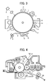
- Fig. 3 is a schematic diagram illustrating an example of the image bearing member.
- a charging device 3 is used as the charging device to uniformly charge the image bearing member.
- known charging devices for example, a corotron device, a scorotron device, a solid discharging element, a needle electrode device, a roller charging device and an electroconductive brush device, can be used.
- an image irradiation portion 5 is used to form a latent electrostatic image on an image bearing member 1 which is uniformly charged.
- typical luminescent materials for example, a fluorescent lamp, a tungsten lamp, a halogen lamp, a mercury lamp, a sodium lamp, a luminescent diode (LED) , a semi-conductor laser (LD) and electroluminescence (EL) can be used.
- Various kinds of filters for example, a sharp cut filter, a band pass filter, an infrared cut filter, a dichroic filter, a coherency filter and a color conversion filter can be used to irradiate the image bearing member 1 with light having only a desired wavelength.
- a developing unit 6 As the developing method, there are a single component development method and a two component development method which use a dry toner and a wet development method which uses a wet toner.
- the image bearing member is positively (negatively) charged and image irradiation is performed, a positive (negative) latent electrostatic image is formed on the surface of the image bearing member 1.
- a positive (negative) latent electrostatic image is developed with a toner (electric detecting particulates) having a negative (positive) polarity, a positive image is obtained.
- a toner having a positive (negative) polarity a negative image is obtained.
- a transfer charging device 9 is used to transfer the visualized toner image on the image bearing member 1 to a transfer medium 9.
- a charging device 7 prior to transfer can be used.
- a transfer device an electrostatic transfer system using a transfer charging device or a bias roller, a mechanical transfer system using an adhesive transfer method or a pressure transfer method, and a magnetic transfer system can be used.
- the electrostatic transfer system the same device as the charging device mentioned above can be used.
- a separation charging device 11 and a separation claw 12 are used as a device to separate the transfer medium 9 from the image bearing member 1.
- electrostatic absorption guiding separation, side end belt separation, front end grip transfer, curvature separation, etc. can be used as the separation charging device 11, the same device as the charging device mentioned above can be used.
- a fur brush 14 and a cleaning blade 15 are used.
- a charging device 13 prior to cleaning can be used.
- Other cleaning devices for example, a web-system device and a magnet brush system device can be also used. These cleaning devices can be used alone or in combination.
- a discharging device is used to remove the latent electrostatic image on the image bearing member 1.
- a discharging lamp 2 and a discharging charger can be used as the discharging device.
- the same devices as the irradiation light sources and the charging devices can be used therefor.
- known devices can be used in the processes of scanning originals, paper feeding, fixing images, discharging recording media, etc., which are performed not in the vicinity of the image bearing member 1.
- the image forming method and the image forming apparatus of the present invention use the image bearing member of the present invention in the image formation device described above.
- This image formation device can be fixedly implemented in a photocopier, a facsimile machine or a printer and also detachably incorporated therein as a form of a process cartridge.
- Fig. 4 is a diagram illustrating an example of the process cartridge.
- a process cartridge for use in the image formation is a device (part) which includes an image bearing member 101 and at least one of a charging device 102, an irradiation device 103, a development device 104, a transfer device 106, a cleaning device 107 and a discharging device (not shown) and detachably attached to the main body of an image forming apparatus.
- the image formation process by the process cartridge illustrated in Fig. 4 is: the image bearing member 101 in rotation is charged with the charging device 52 and irradiated by an irradiating device 53 to form a latent electrostatic image corresponding to the irradiation image on the surface of the image bearing member 101; the latent electrostatic image is developed with toner by the developing device 104; the toner image is transferred to a transfer medium 105 with the transfer device 106; the transferred image is then printed out; On the other hand, the surface of the image bearing member 101 is cleaned after transfer by the cleaning device 57 and discharged by the discharging device (not shown) ; and all the operations mentioned above continues in a repeated manner.
- a process cartridge for use in image formation which integrally has the image bearing member of the present invention having an uncured photosensitive layer and a cross linking surface layer containing a particular cured material and at least one of a charging device, a developing device, a transfer device, a cleaning device and a discharging device.
- the image bearing member of the present invention can be applied not only to an a photocopier using the electrophotographic system, but also widely to the applied electrophotographic field including, for example, a laser beam printer, a CRT printer, an LED printer, a liquid crystal printer, and laser plate making.
- Triphenyl amine derivatives are synthesized by a known method as raw material. For example, Ullman reaction between an iodobenzene derivative and aniline, Ullman reaction between a diphenyl amine derivative and an iodobenzene derivative and a coupling reaction between a diphenayl amine derivative and bromobenzene derivative under the presence of palladium catalyst can be suitably used.
- triphenyl amine derivative (a structure in which para position of at least one benzene ring is non-substituted) is brominated by a known bromination method.
- a method using bromine or a method using N-bromosuccinimide (NBS) test reagent is suitable used.
- a boronation body of bromine group is synthesized by a known method. For example, a method in which a bromine body is treated by butyl lithium and reacted with trialcoxy boran or a method in which a bromine body is subjected to grignard reagent treatment and reacted with trialcoxy boran is suitably used.
- Suzuki-Miura coupling reaction a boronate derivative and a bromobenzene derivative are easily reacted by heating and stirring at 50 to 150 °C with a strong base and triphenyl phosphine palladium catalyst in a suitable solvent such as toluene and ethanol.
- the following recipe is placed in a reaction container equipped with a stirrer, a thermometer, and a condenser and subjected to degassing treatment with ultrasonic wave in a nitrogen atmosphere.
- 1.05 g of tetrakis triphenyl phosphine palladium zero valent complex is added to the reaction container followed by reaction at 70 °C for 7 hours.
- the extracted organic layer is water washed and subject to absorption treatment twice with activated white earth followed by condensation to obtain a coarse product.
- the coarse product is refined with silica gel using column chromatography to obtain the end product (Yield amount: 15.75 g).
- Acrylization or methacrylization is conducted using an esterification reaction of acrylic acid or methacrylic acid and an alcohol derivative.
- an acrylic chloride or a methacrylic chloride can be used.
- easy synthesis is possible by esterification of 3-chloropropanic acid chloride and an alcohol derivative followed by de-hydrochlorization under the presence of a base.
- raw material aniline is acylized (and deacylized after the synthesis of the first N-mono substitution) to avoid production of primary amines, secondary amines, and tertiary amines simultaneously or secondary amines are selectively obtained by refinement (chromatography separation, separation by solubility difference among each salt of amine hydrochlorate to boiled water, etc.).
- the illustrated compound No. 14 is synthesized by preparing a synthesized product (2,4,6-trimethyl-2',4'-dimethyltriphenyl amine), which is prepared by cross coupling reaction between 2, 4-dimethyl diphenyl amine (Tokyo Chemical industry Co., Ltd.) and mesityl bromide (Tokyo Chemical industry Co., Ltd.) using an organic palladium catalyst, and using the same manner as described for the illustrated compound No. 3 for the processes after B1-1 process.
- the detail is described in the synthesis of the illustrated compound No. 14 described below.
- the illustrated compound No. 26 is synthesized in the same manner as in the synthesis method for the illustrated compound No. 3 except that 2- (4-bromophenyl) ethyl alcohol and tetrakis triphenyl phosphine palladium zero valent complex for the illustrated compound No. 3 are replaced with 3- (4-chlorophenyl)propane-1-ol (manufactured by Acros Organic) and bis(tri-tert-butyl phosphine) palladium (0) (Strem Chemicals Inc.) and sodium tert butoxido and orthoxylene are used as the base and the solvent in Suzuki-Miura reaction.
- This can be also synthesized by using 3-(4-iodophenyl)-1-propanol, which can be prepared by iodinizing 3-phenyl-1-propanol under a suitable condition, instead of the hydroxyalkyl substituted bromobenzene derivative.
- the detail is described in the synthesis of the illustrated compound No. 26 described below.
- Suzuki-Miura coupling reaction is known to be conducted by an iodobenzene derivative and a phenyl boronic acid derivative.
- the hydroxyalkyl substituted bromobenzene derivative can be replaced with a hydroxyalkyl substituted iodobenzene derivative.
- the illustrated compound No. 31 is synthesized by synthesizing 2,4, -dimethyl-4' -methyl triphenyl amine according to cross coupling reaction of 2,4-dimethyl diphenyl amine (manufactured by Tokyo Chemical Industry Co., Ltd.) and 4-bromotoluene (manufactured by Tokyo Chemical Industry Co., Ltd.) with an organic palladium catalyst and acrylating a hydroxyl compound prepared by cross coupling reaction between the boronic acid synthesized as described for the illustrated compound No. 3 and 4-(4-hydroxybutyl)bromo benzene.
- the illustrated compound No. 47 can be synthesized in the manner in which N-mono substitution is synthesized and refined with acylized aniline in an amount corresponding to the half amount of p-iodotoluene for use in the illustrated compound No. 3, p-iodomethoxybenzene is reacted with the refined N-mono substitution and 4-bromophenethyl alcohol for use in the synthesis of the illustrated compound No. 3 is changed to 3-(4-bromophenyl)-sec-butyl alcohol.
- 4-diphenylaminophenyl boronic acid is used to prepare 2-(4'-diphenylamino)biphenyl-4-yl)ethyl alcohol in the same manner as in synthesis of 2-(4'-(di-p-tolylamino)bihpneyl-4-il)ethyl alcohol.
- 8.1 g and 80 ml of N,N-dimethylacetamide are placed in a reaction container.
- 4.22 g of 3-chloropropionyl chloride is dripped thereto in 15 minutes while cooled with ice.
- the coarse product is dissolved in 250 ml of toluene and 10 g of activated white earth (manufactured by Wako Pure Chemical Industries Ltd.) which has been dried at 130 °C beforehand is added thereto followed by a 30 minute stirring.
- the activated white earth is removed with filtration and the filtered resultant is condensed with an evaporator.
- the resultant is column fined using silica gel (60 N, manufactured by Merck Ltd.) with toluene as a developing solvent.
- the resultant is re-crystallized with a mixture solvent of ethanol and toluene to obtain 8.18 g of 2-(4'-(diphenylamino)biphenyl-4-yl)ethyl acrylate (target substance), which is non-color needle like crystal with the melting point of from 105.5 to 106.5 °C.
- the crystal is ionized by an atmospheric pressure chemical ionization method.
- the m/z value measured in the positive mode is 420 and matches the value obtained by adding 1 of proton to the molecular weight calculated by the molecular formula.
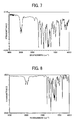
- the IR spectrum is measured and the result thereof is shown in Fig. 5 .
- the coarse product is dissolved in 250 ml of toluene and 10 g of activated white earth (manufactured by Wako Pure Chemical Industries Ltd.) which has been dried at 130 °C beforehand is added thereto followed by a 30 minute stirring.
- the activated white earth is removed with filtration and the filtered resultant is condensed with an evaporator.
- the resultant is column fined using silica gel (60 N, manufactured by Merck Ltd.) with toluene as a developing solvent.
- silica gel 60 N, manufactured by Merck Ltd.
- the oil is ionized by an atmospheric pressure chemical ionization method.
- the m/z value measured in the positive mode is 437 and matches the value obtained by adding 1 of proton to the molecular weight calculated by the molecular formula.
- the IR spectrum is measured and the result thereof is shown in Fig. 6 .
- reaction solution is filtered using silica gel and the solvent is removed to obtain 39 g of a coarse product.
- the coarse product is column fined using silica gel to obtain 24.5 g of the target substance of non-color crystal of 2,4-dimethyl-4'-methyltriphenyl amine.
- the melting point thereof is from 76.5 to 78.0 °C.
- the resultant is column fined using silica gel (60 N, manufactured by Merck Ltd.) with toluene as a developing solvent and thus, 4.46 g of the target substance (non-color oil) of 2-(4'-(2,4-dimethylphenyl(4-methylphenyl)amino)biphenyl-4-yl)ethy 1 acrylate is obtained.
- the oil is ionized by an atmospheric pressure chemical ionization method.
- the m/z value measured in the positive mode is 462 and matches the value obtained by adding 1 of proton to the molecular weight calculated by the molecular formula.
- the IR spectrum is measured and the result thereof is shown in Fig. 7 .
- 3,4-dimethyl-4'-methyltriphenyl amine is synthesized from 4-methyldiphenyl amine and 4-bromo-o-xylene in the same manner as in 2,4-dimethyl-4'methyltriphenyl amine.
- 13.78 g of 4-bromo-3',4'-dimethyl-4"-methyltriphenyl amine synthesized from 3,4-dimethyl-4'-methyltriphenyl amine as in synthesis of 4-bromo-2',4'-dimethyl-4"-methyltriphenyl amine is dissolved in 100 ml of tetrahydrofuran and cooled down to -76 °C in nitrogen atmosphere.
- the liquid extraction is washed with saturated saline three times and dehydrated with sodium sulfonate.
- the solvent is removed by an evaporator to obtain 6.87 g of a coarse product.
- the coarse product is column fined using silica gel (60 N, manufactured by Merck Ltd.) with toluene as a developing solvent and thus, 5.5 g of the target substance (non-color oil) of 2-(4'-(3,4-dimethylphenyl(4-methylphenyl)amino)biphenyl-4-yl) ethyl acrylate is obtained.
- the oil is ionized by an atmospheric pressure chemical ionization method.
- the m/z value measured in the positive mode is 462 and matches the value obtained by adding 1 of proton to the molecular weight calculated by the molecular formula.
- the IR spectrum is measured and the result thereof is shown in Fig. 8 .
- 2,4,6-trimethyl-4'-methyltriphenyl amine is synthesized from 4-methyldiphenyl amine and mesityl bromide in the same manner as in synthesis of 2,4-dimethyl-4'methyltriphenyl amine.
- 17.58 g of 4-bromo-2',4',6'-trimethyl-4"-methyltriphenyl amine synthesized from 2,4,6-trimethyl-4'-methyltriphenyl amine as in synthesis of 4-bromo-2',4'-dimethyl-4"-methyltriphenyl amine is dissolved in 150 ml of tetrahydrofuran and cooled down to -75 °C in nitrogen atmosphere.
- the reaction solution is poured into 500 ml of water and hydrochloric acid is added while stirred in order that pH thereof is 4.
- the reaction product is extracted by 300 ml of ethyl acetate and then washed with water three times.
- the solvent is removed by an evaporator to obtain 14 g of a coarse product.
- the coarse product is dissolved in 300 ml of toluene and 10 g of activated white earth (manufactured by Wako Pure Chemical Industries Ltd.) which has been dried at 130 °C beforehand is added thereto followed by a 30 minute stirring.
- the activated white earth is removed with filtration and the filtered resultant is condensed with an evaporator.
- the resultant is column fined using silica gel (60 N, manufactured by Merck Ltd.) with toluene as a developing solvent and thus, 10.5 g of the target substance (non-color oil) of 2-(4'-(2,4,6-trimethylphenyl(4-methylphenyl)amino)biphenyl-4-yl) ethyl acrylate is obtained.
- the oil is ionized by an atmospheric pressure chemical ionization method.
- the m/z value measured in the positive mode is 476 and matches the value obtained by adding 1 of proton to the molecular weight calculated by the molecular formula.
- the IR spectrum is measured and the result thereof is shown in Fig. 9 .
- 2,4-dimethyl-3',4'-dimethyltriphenyl amine is synthesized from 2,4-dimethyldiphenyl amine and 4-bromo-o-xylene in the same manner as in 2,4-dimethyl-4'methyltriphenyl amine.
- 15.4 g of 4-bromo-2',4'-dimethyl-3",4"-dimethyltriphenyl amine synthesized from 2,4-dimethyl-3',4'-dimethyltriphenyl amine as in synthesis of 4-bromo-2',4'-dimethyl-4"-methyltriphenyl amine is dissolved in 100 ml of tetrahydrofuran and cooled down to -75 °C in nitrogen atmosphere.
- the reaction solution is poured into 200 ml of water and hydrochloric acid is added while stirred in order that pH thereof is 4.
- the reaction product is extracted by 300 ml of ethyl acetate and then washed with water three times.
- the solvent is removed by an evaporator to obtain 11 g of a coarse product.
- the coarse product is dissolved in 200 ml of toluene and 9 g of activated white earth (manufactured by Wako Pure Chemical Industries Ltd.) which has been dried at 130 °C beforehand is added thereto followed by a 30 minute stirring.
- the activated white earth is removed with filtration and the filtered resultant is condensed with an evaporator.
- the resultant is column fined using silica gel (60 N, manufactured by Merck Ltd.) with toluene as a developing solvent and thus, 9.94 g of the target substance (light yellow colored oil) of 2-(4'-(2,4-dimethylphenyl(3,4-dimethylphenyl)amino)biphenyl-4-yl) ethyl acrylate is obtained.
- the oil is ionized by an atmospheric pressure chemical ionization method.
- the m/z value measured in the positive mode is 476 and matches the value obtained by adding 1 of proton to the molecular weight calculated by the molecular formula.
- the IR spectrum is measured and the result thereof is shown in Fig. 10 .
- 2,4-dimethyl-2',4',6'-trimethyltriphenyl amine is synthesized from 2,4-dimethylphenyl amine and mesityl bromide in the same manner as in synthesis of 2,4-dimethyl-4'methyltriphenyl amine.
- the reaction product is extracted by 300 ml of ethyl acetate and then washed with water three times. The liquid extraction is furthermore washed with water three times. The solvent is removed by an evaporator to obtain 10.29 g of a coarse product.
- the coarse product is dissolved in 200 ml of toluene and 9 g of activated white earth (manufactured by Wako Pure Chemical Industries Ltd.) which has been dried at 130 °C beforehand is added thereto followed by a 30 minute stirring.
- the activated white earth is removed with filtration and the filtered resultant is condensed with an evaporator.
- the resultant is column fined using silica gel (60 N, manufactured by Merck Ltd.) with toluene as a developing solvent and thus, 9 g of the target substance (non-color oil) of 2-(4'-(2,4-dimethylphenyl(2,4,6-trimethylphenyl)amino)biphenyl-4-yl) ethyl acrylate is obtained.
- the oil is ionized by an atmospheric pressure chemical ionization method.
- the m/z value measured in the positive mode is 490 and matches the value obtained by adding 1 of proton to the molecular weight calculated by the molecular formula.
- the IR spectrum is measured and the result thereof is shown in Fig. 11 .
- 3,4-dimethyl-3',4'-dimethyltriphenyl amine is synthesized from bis(3,4-dimethylphenyl)amine and bromobenzene as in the synthesis of 2,4-dimethyl-4'-methyl triphenyl amine. Bromination and boronization are conducted thereafter as in the synthesis of the illustrated compound No. 8 to synthesize 4-(bis(3,4-dimethylphenyl)amino)phenyl boronic acid.
- the reaction product is extracted by 300 ml of ethyl acetate and then washed with water three times. The solvent is removed by an evaporator to obtain 9.94 g of a coarse product.
- the coarse product is dissolved in 180 ml of toluene and 8 g of activated white earth (manufactured by Wako Pure Chemical Industries Ltd.) which has been dried at 130 °C beforehand is added thereto followed by a 30 minute stirring.
- the activated white earth is removed with filtration and the filtered resultant is condensed with an evaporator.
- the resultant is column fined using silica gel (60 N, manufactured by Merck Ltd.) with toluene as a developing solvent and thus, 7.88 g of the target substance (non-color crystal having a melting point of from 86.5 to 87.5 °C) of 2-(4'-(bis(3,4-dimethylphenyl)amino)biphenyl-4-yl) ethyl acrylate is obtained.
- the crystal is ionized by an atmospheric pressure chemical ionization method.
- the m/z value measured in the positive mode is 476 and matches the value obtained by adding 1 of proton to the molecular weight calculated by the molecular formula.
- the IR spectrum is measured and the result thereof is shown in Fig. 12 .
- the solvent is removed to obtain 81.12 g of the light yellow colored oily target substance.
- the substance is a mixture of 79 % of 3-(4-iodophenyl) propyl acetate and 21 % of 3-(2-iodophenyl) propyl acetate.
- the substance is a mixture of 78 % of 3(4-iodophenyl)-1-propanol and 22 % of 3-(2-iodophenyl)-1-propanol.
- the absorption peak area ratio at a wavelength of 254 nm is 99.8 % and no product derived from 3-(2-iodophenyl)-1-propanol is contained.
- the reaction product is extracted by 300 ml of ethyl acetate and then washed with water three times. The solvent is removed by an evaporator to obtain 6.23 g of a coarse product.
- the coarse product is dissolved in 130 ml of toluene and 5 g of activated white earth (manufactured by Wako Pure Chemical Industries Ltd.) which has been dried at 130 °C beforehand is added thereto followed by a 30 minute stirring.
- the activated white earth is removed with filtration and the filtered resultant is condensed with an evaporator.
- the resultant is column fined using silica gel (60 N, manufactured by Merck Ltd.) with toluene as a developing solvent and thus, 5.65 g of the target substance (non-color oil) of 3-(4'-(di-p-tolylamino)biphenyl-4-yl) propyl acrylate is obtained.
- the oil is ionized by an atmospheric pressure chemical ionization method.
- the m/z value measured in the positive mode is 462 and matches the value obtained by adding 1 of proton to the molecular weight calculated by the molecular formula.
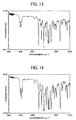
- the IR spectrum is measured and the result thereof is shown in Fig. 13 .
- the solvent is removed to obtain 106.16 g of the light yellow colored oily target substance.
- the substance is a mixture of 79 % of 4- (4-iodophenyl) butyl acetate and 21 % of 4-(2-iodophenyl) butyl acetate.
- the substance is a mixture of 79 % of 4-(4-iodophenyl)-1-butanol and 21 % of 4-(2-iodophenyl)-1-butanol.
- the absorption peak area ratio at a wavelength of 254 nm is 99.2 % and no product derived from 4-(2-iodophenyl)-1-butanol is contained.
- the product is extracted by 300 ml of ethyl acetate and then washed with water three times. The solvent is removed by an evaporator to obtain 7.1 g of a coarse product.
- the coarse product is dissolved in 125 ml of toluene and 5 g of activated white earth (manufactured by Kanto Chemical Co., Inc.) which has been dried at 130 °C beforehand is added thereto followed by a 30 minute stirring.
- the activated white earth is removed with filtration and the filtered resultant is condensed with an evaporator.
- the resultant is column fined using silica gel (60 N, manufactured by Merck Ltd.) with toluene as a developing solvent and thus, 6.51 g of the target substance (non-color oil) of 4-(4'-(di-p-tolylamino)biphenyl-4-yl) butyl acrylate is obtained.
- the oil is ionized by an atmospheric pressure chemical ionization method.
- the m/z value measured in the positive mode is 476 and matches the value obtained by adding 1 of proton to the molecular weight calculated by the molecular formula.
- the IR spectrum is measured and the result thereof is shown in Fig. 14 . Synthesis of Illustrated Compound No. 35
- the solvent is removed to obtain 48.6 g of the light yellow colored oily target substance.
- the substance is a mixture of 79 % of 5-(4-iodophenyl) pentyl acetate and 21 % of 5-(2-iodophenyl) pentyl acetate.
- the substance is a mixture of 79 % of 5-(4-iodophenyl)-1-pentanol and 21 % of 5-(2-iodophenyl)-1-pentanol.
- the absorption peak area ratio at a wavelength of 254 nm is 99.6 % and no product derived from 5-(2-iodophenyl)-1-pentanol is contained.
- the reaction product is extracted by 300 ml of ethyl acetate and then washed with water three times. The solvent is removed by an evaporator and the resultant is dissolved in 125 ml of toluene.
- 5.5 g of activated white earth (manufactured by Kanto Chemical Co., Inc.) which has been dried at 130 °C beforehand is added thereto followed by a 30 minute stirring. The activated white earth is removed with filtration and the filtered resultant is condensed with an evaporator.
- the resultant is column fined using silica gel (60 N, manufactured by Merck Ltd.) with toluene as a developing solvent and thus, 6.88 g of the target substance (non-color oil) of 5-(4'-(di-p-tolylamino)biphenyl-4-yl) pentyl acrylate is obtained.
- the oil is ionized by an atmospheric pressure chemical ionization method.
- the m/z value measured in the positive mode is 490 and matches the value obtained by adding 1 of proton to the molecular weight calculated by the molecular formula.
- the IR spectrum is measured and the result thereof is shown in Fig. 15 .
- the liquid application for an undercoat layer, the liquid application for a charge generating layer and a liquid application for a charge transport layer of the following composition are sequentially applied and dried to form an undercoat layer having a thickness of 3.5 ⁇ m, a charge generating layer having a thickness of 0.2 ⁇ m, and a charge transport layer having a thickness of 15 ⁇ m.
- the liquid application for cross linking surface layer is spray coated and naturally dried for 20 minutes followed by irradiation under the following conditions for curing the coated layer.
- the coated layer is dried for 20 minutes at 130 °C and an image bearing member of the present invention having a cross linking surface layer of 12 ⁇ m is thus obtained.
- Example 2 The image bearing member of Example 2 is manufactured in the same manner as in Example 1 except that the liquid application for cross linking surface layer of Example 1 is changed to the following:
- Example 3 The image bearing member of Example 3 is manufactured in the same manner as in Example 1 except that the liquid application for cross linking surface layer of Example 1 is changed to the following:
- the image bearing member of Example 4 is manufactured in the same manner as in Example 1 except that the diameter of the aluminum cylinder of Example 1 is changed to 100 mm, and the liquid application for charge generation layer and the liquid application for cross linking surface layer of Example 1 are changed to the following:
- the image bearing member of Example 5 is manufactured in the same manner as in Example 4 except that the liquid application for cross linking surface layer of Example 4 is changed to the following:
- the image bearing member of Example 6 is manufactured in the same manner as in Example 4 except that the liquid application for cross linking surface layer of Example 4 is changed to the following:
- the image bearing member of Example 7 is manufactured in the same manner as in Example 1 except that the layer thickness of the cross linking surface layer in Example 1 is changed to 15 ⁇ m.
- the image bearing member of Example 8 is manufactured in the same manner as in Example 4 except that the layer thickness of the cross linking surface layer in Example 4 is changed to 15 ⁇ m.
- Example 9 The image bearing member of Example 9 is manufactured in the same manner as in Example 4 except that the illustrated compound No. 26 of the radical reactive compound is replaced with the illustrated compound No. 1.
- Example 10 The image bearing member of Example 10 is manufactured in the same manner as in Example 4 except that the illustrated compound No. 26 of the radical reactive compound is replaced with the illustrated compound No. 2.
- Example 11 The image bearing member of Example 11 is manufactured in the same manner as in Example 4 except that the illustrated compound No. 26 of the radical reactive compound is replaced with the illustrated compound No. 8.
- Example 12 The image bearing member of Example 12 is manufactured in the same manner as in Example 4 except that the illustrated compound No. 26 of the radical reactive compound is replaced with the illustrated compound No. 9.
- Example 13 The image bearing member of Example 13 is manufactured in the same manner as in Example 4 except that the illustrated compound No. 26 of the radical reactive compound is replaced with the illustrated compound No. 10.
- Example 14 The image bearing member of Example 14 is manufactured in the same manner as in Example 4 except that the illustrated compound No. 26 of the radical reactive compound is replaced with the illustrated compound No. 13.
- Example 15 The image bearing member of Example 15 is manufactured in the same manner as in Example 4 except that the illustrated compound No. 26 of the radical reactive compound is replaced with the illustrated compound No. 16.
- Example 16 The image bearing member of Example 16 is manufactured in the same manner as in Example 4 except that the illustrated compound No. 26 of the radical reactive compound is replaced with the illustrated compound No. 30.
- Example 17 The image bearing member of Example 17 is manufactured in the same manner as in Example 4 except that the illustrated compound No. 26 of the radical reactive compound is replaced with the illustrated compound No. 35.
- the image bearing member of comparative Example 1 is manufactured in the same manner as in Example 1 except that the cross linking surface layer of Example 1 is not provided and the layer thickness of the charge transport layer of Example 1 is changed to 27 ⁇ m.
- the image bearing member of comparative Example 2 is manufactured in the same manner as in Example 4 except that the cross linking surface layer of Example 1 is not provided and the layer thickness of the charge transport layer of Example 4 is changed to 27 ⁇ m.
- the image bearing member of comparative Example 3 is manufactured in the same manner as in Example 1 except that the radical reactive compound for use in the liquid application for cross linking surface layer of Example 1 is changed to a compound represented by the following chemical formula 3:
- the image bearing member of comparative Example 4 is manufactured in the same manner as in Example 2 except that the radical reactive compound for use in the liquid application for cross linking surface layer of Example 2 is changed to a compound represented by the following chemical formula 3:
- the image bearing member of comparative Example 5 is manufactured in the same manner as in Example 2 except that the radical reactive compound for use in the liquid application for cross linking surface layer of Example 2 is changed to a compound represented by the following chemical formula 4:
- the image bearing member of comparative Example 6 is manufactured in the same manner as in Example 4 except that the radical reactive compound for use in the liquid application for cross linking surface layer of Example 4 is changed to a compound represented by the following chemical formula 5
- the image bearing member of comparative Example 7 is manufactured in the same manner as in Example 4 except that the radical reactive compound for use in the liquid application for cross linking surface layer of Example 4 is changed to a compound represented by the following chemical formula 6:
- the image bearing member of comparative Example 8 is manufactured in the same manner as in Example 4 except that the radical reactive compound for use in the liquid application for cross linking surface layer of Example 4 is changed to a compound represented by the following chemical formula 7:
- the image bearing member of comparative Example 9 is manufactured in the same manner as in Example 4 except that the radical reactive compound for use in the liquid application for cross linking surface layer of Example 4 is changed to a compound represented by the following chemical formula 8:
- the image bearing member of comparative Example 10 is manufactured in the same manner as in Example 4 except that the radical reactive compound for use in the liquid application for cross linking surface layer of Example 4 is changed to a compound represented by the following chemical formula 9:
- the image bearing member of comparative Example 11 is manufactured in the same manner as in Example 4 except that the radical reactive compound for use in the liquid application for cross linking surface layer of Example 4 is changed to a compound represented by the following chemical formula 10:
- the amount of abrasion (the value obtained by subtracting the layer thickness of the image bearing member after photocopying from the layer thickness before photocopying) and the surface voltage at the development portion for a solid image (the values for the initial photocopying and after 50, 000 image formation) are measured.
- the results are shown in Table 2.
- the amount of abrasion (the value obtained by subtracting the layer thickness of the image bearing member after photocopying from the layer thickness before photocopying) and the surface voltage at the development portion for a solid image (the values for the initial photocopying and after 50, 000 image formation) are measured while the process control is off.
- the results are shown in Tables 2.
- the image bearing members of Examples of the present invention have by far better anti-abrasion property than a typical organic image bearing member having no protective layer.
- the image bearing members of Examples are at the best level with regard to the anti-abrasion property, have an excellent voltage decay characteristic and can maintain the voltage decay characteristic while variously fatigued over the operation.
- the image bearing members of Examples have the characteristics mentioned above even though the image bearing members have a relatively thick protective layer in comparison with a typical protective layer. Due to these characteristics, the image bearing member of the present invention has an extremely long life.
- the image bearing members of Comparative Examples are good, but the surface voltage at the development portion is already high at the beginning for a solid image for all the image bearing members of Comparative Examples. Therefore, the voltage difference between the irradiated portion and the non-irradiated portion is small so that the image density tends to fluctuate.
- the image bearing members are good at charge transport and the surface voltage of the development portion is small from the initial and the variation thereof is small even after the image bearing members are fatigued. Consequently, the image bearing members of the present invention can produce quality images stably for an extended period of time.
- Example 1 When Example 1 is compared with Examples 2 and 3, it is found that the anti-abrasion property is improved due to the initiator. Therefore, it is possible to provide an image bearing member having excellent anti-abrasion property when an initiator is used in combination.
- the image bearing member of the present invention it is possible to provide a reliable high performance image forming apparatus and process cartridge which can produce quality images for an extended period of time.
- the applied layer before irradiation of ultraviolet is left for one day and whether the applied layer is kept uniform is observed by naked eyes.
- the applied layer is irradiated with ultraviolet for cross-lniking and the state thereof is observed by naked eyes.
- each sample of the applied layer before irradiation of ultraviolet observed after a short while is smooth and uniform.
- turbidity is observed in the liquid application for the cross linking surface layer for use in Example 9 due to phase separation and remains after cross-linked.
- turbidity is slightly observed in the liquid applications for the cross linking surface layer for use in Examples 2 and 16 and remains after cross-linked.
- the physical propertyies of the radical reactive compounds for use in the samples in which turbidity is observed are compared with those for use in the samples in which turbidity is not observed, the occurrence of turbidity depends on whether the radical reactive compounds are obtained as crystal, or amorphous or oily substance as in the synthesis results. That is, the radical reactive compounds obtained as crystal are easily crystallized so that crystallization occurs when the compounds are left for a long time, which leads to phase separation. On the other hand, the radical reactive compounds obtained as amorphous or oily substance are hardly crystallized, which is considered to be a reason for avoiding phase separation.
- the degree of ease of crystallization relates to the length of the alkylene group represented by X and the symmetry property of the phenyl groups connected to the nitrogen atom in Chemical formula B. That is, when X in Chemical formula B is ethylene group, which has 2 carbon atoms, and the phenyl group having R 1 to R 5 and the phenyl group having R 1 ' to R 5 ' are different from each other (i.e., assymeetric), crystallization hardly occurs.
Landscapes
- Physics & Mathematics (AREA)
- Chemical & Material Sciences (AREA)
- General Physics & Mathematics (AREA)
- Organic Chemistry (AREA)
- Spectroscopy & Molecular Physics (AREA)
- Chemical Kinetics & Catalysis (AREA)
- Photoreceptors In Electrophotography (AREA)
Claims (15)
- Elément supportant une image comprenant :un substrat électroconducteur ;une couche photosensible disposée sur le substrat électroconducteur ; etune couche de surface réticulée comprenant le composé durcissant de transport de charge et disposée sur la couche photosensible,dans lequel le composé durcissant de transport de charge comprend un matériau comprenant une unité de structure représentée par la formule chimique A suivante :

- Elément supportant une image selon la revendication 1, dans lequel X est un groupe éthylène et un groupe phényle présentant les groupes R1 à R5 est différent d'un groupe phényle présentant les groupes R1' à R5'.
- Elément supportant une image selon la revendication 1, dans lequel X est un groupe alkylène à chaîne linéaire ayant de 3 à 5 atomes de carbone.
- Elément supportant une image selon l'une quelconque des revendications 1 à 3, dans lequel le composé durcissant de transport de charge est formé par application d'une application liquide comprenant le composé représenté par la formule chimique A et un monomère présentant au moins trois groupes fonctionnels polymérisables sur une surface de la couche photosensible suivie par un durcissement.
- Elément supportant une image selon la revendication 4, dans lequel l'application liquide comprend de plus un initiateur de polymérisation.
- Elément supportant une image selon l'une quelconque des revendications 1 à 5, dans lequel la couche de surface réticulée est formée sur la couche photosensible et la couche photosensible est non durcie.
- Elément supportant une image selon l'une quelconque des revendications 1 à 6, dans lequel le composé durcissant de transport de charge est formé par un dispositif utilisant une énergie optique.
- Elément supportant une image selon l'une quelconque des revendications 1 à 7, dans lequel la couche photosensible présente une structure dans laquelle une couche de génération de charge et une couche de transport de charge sont successivement accumulées sur le substrat électroconducteur.
- Procédé de fabrication d'un élément supportant une image comprenant :le dépôt d'une application liquide comprenant un composé réactif radicalaire représenté par la formule chimique B suivante sur une surface de la couche photosensible de l'élément supportant une image selon la revendication 1 ; etle durcissement de l'application liquide pour former le composé
durcissant de transport de charge ;
- Procédé de fabrication d'un élément supportant une image selon la revendication 9, dans lequel X dans la formule chimique B est un groupe éthylène et un groupe phényle présentant les groupes R1 à R5 est différent d'un groupe phényle présentant les groupes R1' à R5'.
- Procédé de fabrication d'un élément supportant une image selon la revendication 9, dans lequel X dans la formule chimique B est un groupe alkylène à chaîne linéaire ayant de 3 à 5 atomes de carbone.
- Procédé de formation d'une image comprenant :le chargement de l'élément supportant une image selon la revendication 1 ;l'irradiation de l'élément supportant une image pour former une image électrostatique latente sur l'élément supportant une image ;le développement de l'image électrostatique latente avec un agent de développement pour former une image développée ; etle transfert de l'image développée sur un support d'enregistrement.
- Appareil formant une image comprenant :l'élément supportant une image selon la revendication 1 ;un dispositif de chargement configuré pour charger l'élément supportant une image ;un dispositif d'irradiation configuré pour irradier l'élément supportant une image avec de la lumière afin de former une image électrostatique latente sur l'élément supportant une image ;un dispositif de développement configuré pour développer l'image électrostatique latente avec un agent de développement ;un dispositif de transfert configuré pour transférer l'image développée sur un support d'enregistrement.
- Cartouche de procédé comprenant :l'élément supportant une image selon la revendication 1 ; etau moins un dispositif choisi dans le groupe constitué d'un dispositif de chargement, d'un dispositif d'irradiation, d'un dispositif de développement, d'un dispositif de transfert, d'un dispositif de nettoyage et d'un dispositif de déchargement,dans laquelle l'élément supportant une image et le au moins un dispositif sont structurés en une seule pièce et la cartouche de procédé peut être fixée de manière détachable à un appareil formant une image.
- Composé réactif radicalaire représenté par la formule chimique B :

Applications Claiming Priority (2)
| Application Number | Priority Date | Filing Date | Title |
|---|---|---|---|
| JP2007151766 | 2007-06-07 | ||
| JP2008125017A JP5453733B2 (ja) | 2007-06-07 | 2008-05-12 | 電子写真感光体、それを用いた画像形成方法、画像形成装置及び画像形成装置用プロセスカートリッジ |
Publications (2)
| Publication Number | Publication Date |
|---|---|
| EP2000855A1 EP2000855A1 (fr) | 2008-12-10 |
| EP2000855B1 true EP2000855B1 (fr) | 2011-08-03 |
Family
ID=39673015
Family Applications (1)
| Application Number | Title | Priority Date | Filing Date |
|---|---|---|---|
| EP08157717A Active EP2000855B1 (fr) | 2007-06-07 | 2008-06-06 | Élément supportant une image, son procédé de fabrication, procédé et appareil de formation d'images et cartouche de traitement |
Country Status (2)
| Country | Link |
|---|---|
| US (1) | US20080304867A1 (fr) |
| EP (1) | EP2000855B1 (fr) |
Families Citing this family (7)
| Publication number | Priority date | Publication date | Assignee | Title |
|---|---|---|---|---|
| JP4702447B2 (ja) * | 2008-12-25 | 2011-06-15 | 富士ゼロックス株式会社 | 電子写真感光体、プロセスカートリッジ、及び画像形成装置 |
| US8791800B2 (en) | 2010-05-12 | 2014-07-29 | Nokia Corporation | Detecting touch input and generating perceptible touch stimulus |
| US8652717B2 (en) * | 2010-12-27 | 2014-02-18 | Ricoh Company, Ltd. | Image bearing member and image forming method, image forming apparatus, and process cartridge using the same |
| JP6481324B2 (ja) | 2013-12-13 | 2019-03-13 | 株式会社リコー | 電子写真感光体、電子写真方法、電子写真装置及びプロセスカートリッジ |
| JP6711107B2 (ja) | 2016-04-25 | 2020-06-17 | 株式会社リコー | 感光体、画像形成装置、及びプロセスカートリッジ |
| JP6769112B2 (ja) | 2016-05-25 | 2020-10-14 | 株式会社リコー | 電子写真感光体、画像形成装置、及びプロセスカートリッジ |
| JP6781396B2 (ja) | 2016-05-30 | 2020-11-04 | 株式会社リコー | 感光体、画像形成装置及びプロセスカートリッジ |
Family Cites Families (29)
| Publication number | Priority date | Publication date | Assignee | Title |
|---|---|---|---|---|
| US5322753A (en) * | 1991-07-12 | 1994-06-21 | Ricoh Company, Ltd. | Electrophotographic photoconductor and acrylic acid ester polymer for use in the same |
| JPH0769126B2 (ja) | 1992-02-07 | 1995-07-26 | 紘明 塚谷 | 切削工具の刃先精度検出方法 |
| JPH0645770A (ja) | 1992-07-22 | 1994-02-18 | Toshiba Corp | 筐体装置 |
| US5427880A (en) * | 1993-02-01 | 1995-06-27 | Ricoh Company, Ltd. | Electrophotographic Photoconductor |
| JP3262488B2 (ja) | 1996-02-19 | 2002-03-04 | キヤノン株式会社 | 電子写真感光体、それを用いた電子写真装置および装置ユニット |
| JPH09319113A (ja) * | 1996-05-24 | 1997-12-12 | Ricoh Co Ltd | 電子写真感光体 |
| JP3773238B2 (ja) * | 1999-04-30 | 2006-05-10 | 株式会社リコー | 電子写真感光体、その物を有するプロセスカートリッジ及び電子写真装置 |
| JP4093725B2 (ja) * | 2000-04-05 | 2008-06-04 | 株式会社リコー | 電子写真感光体、それを用いる画像形成方法、画像形成装置及び画像形成装置用プロセスカートリッジ |
| US6998209B2 (en) * | 2002-02-21 | 2006-02-14 | Ricoh Company, Ltd. | Electrophotographic photoreceptor, and electrophotographic apparatus, process cartridge and method using the photoreceptor |
| US7279260B2 (en) * | 2002-06-12 | 2007-10-09 | Ricoh Company, Ltd. | Electrophotographic photoconductor having a crosslinked resin layer and method of preparing an electrophotographic photoconductor |
| US7179573B2 (en) * | 2003-03-20 | 2007-02-20 | Ricoh Company, Ltd. | Electrophotographic photoconductor, and image forming process, image forming apparatus and process cartridge for an image forming apparatus using the same |
| US7175957B2 (en) * | 2003-03-20 | 2007-02-13 | Ricoh Company, Ltd. | Electrophotographic photoconductor, and image forming process, image forming apparatus and process cartridge for an image forming apparatus using the same |
| JP4497969B2 (ja) * | 2004-03-19 | 2010-07-07 | 株式会社リコー | 電子写真感光体、それを用いた画像形成方法、画像形成装置及び画像形成装置用プロセスカートリッジ |
| US7473504B2 (en) * | 2004-05-25 | 2009-01-06 | Ricoh Company, Ltd. | Electrophotographic photoreceptor, and image forming method, apparatus and process cartridge therefor using the photoreceptor |
| JP4144755B2 (ja) * | 2004-06-24 | 2008-09-03 | 株式会社リコー | 電子写真感光体、それを用いた画像形成方法、画像形成装置及び画像形成装置用プロセスカートリッジ |
| JP4189923B2 (ja) * | 2004-06-25 | 2008-12-03 | 株式会社リコー | 画像形成方法及びこれを用いた画像形成装置、プロセスカートリッジ |
| JP4767523B2 (ja) * | 2004-07-05 | 2011-09-07 | 株式会社リコー | 電子写真感光体、それを用いた画像形成方法、画像形成装置及び画像形成装置用プロセスカートリッジ |
| JP4440073B2 (ja) * | 2004-09-03 | 2010-03-24 | 株式会社リコー | 静電潜像担持体及びプロセスカートリッジ、並びに、画像形成装置及び画像形成方法 |
| JP4249681B2 (ja) * | 2004-09-06 | 2009-04-02 | 株式会社リコー | 画像形成装置及びプロセスカートリッジ |
| JP2006091117A (ja) * | 2004-09-21 | 2006-04-06 | Ricoh Co Ltd | 画像形成方法及び画像形成装置 |
| US20060093955A1 (en) * | 2004-11-01 | 2006-05-04 | Kohichi Ohshima | Image forming method, and image forming apparatus and process cartridge using the image forming method |
| JP4248483B2 (ja) * | 2004-11-19 | 2009-04-02 | 株式会社リコー | 電子写真感光体、その製造方法、それを使用した画像形成方法、画像形成装置及び画像形成装置用プロセスカートリッジ |
| EP1674940B1 (fr) * | 2004-12-24 | 2008-11-26 | Ricoh Company, Ltd. | Photorécepteur électrophotographique et procédé de formation d'images, appareil de formation d'image et cartouche de traitement correspondante utilisant le photorécepteur |
| US7507511B2 (en) * | 2005-01-14 | 2009-03-24 | Ricoh Company Ltd. | Electrophotographic photoreceptor, and image forming apparatus and process cartridge therefor using the electrophotographic photoreceptor |
| JP2006227761A (ja) | 2005-02-15 | 2006-08-31 | Sharp Corp | 通信装置 |
| US7914959B2 (en) * | 2005-11-28 | 2011-03-29 | Ricoh Company, Limited | Image bearing member, image forming method, and image forming apparatus |
| JP2007153765A (ja) * | 2005-12-01 | 2007-06-21 | Ricoh Co Ltd | テトラヒドロキシ化合物 |
| US7858278B2 (en) * | 2006-05-18 | 2010-12-28 | Ricoh Company Limited | Electrophotographic photoreceptor, and image forming apparatus and process cartridge using the electrophotographic photoreceptor |
| JP4668853B2 (ja) * | 2006-06-16 | 2011-04-13 | 株式会社リコー | 電子写真感光体、並びにこれを用いた画像形成装置及びプロセスカートリッジ |
-
2008
- 2008-05-30 US US12/156,134 patent/US20080304867A1/en not_active Abandoned
- 2008-06-06 EP EP08157717A patent/EP2000855B1/fr active Active
Also Published As
| Publication number | Publication date |
|---|---|
| EP2000855A1 (fr) | 2008-12-10 |
| US20080304867A1 (en) | 2008-12-11 |
Similar Documents
| Publication | Publication Date | Title |
|---|---|---|
| EP1742112B1 (fr) | Photorécepteur électrophotographique, procédé de préparation du photorécepteur, procédé et appareil de formation d'images et cartouche de processus correspondante utilisant le photorécepteur électrophotographique | |
| EP1674940B1 (fr) | Photorécepteur électrophotographique et procédé de formation d'images, appareil de formation d'image et cartouche de traitement correspondante utilisant le photorécepteur | |
| US8043773B2 (en) | Image bearing member, image forming apparatus and process cartridge | |
| JP2006145880A (ja) | 電子写真感光体、その製造方法、それを使用した画像形成方法、画像形成装置及び画像形成装置用プロセスカートリッジ | |
| US20070031746A1 (en) | Electrophotographic photoconductor, process cartridge, and image forming method | |
| EP2000855A1 (fr) | Élément supportant une image, son procédé de fabrication, procédé et appareil de formation d'images et cartouche de traitement | |
| JP5532194B2 (ja) | 重合性化合物、該重合性化合物を用いた電子写真感光体、該電子写真感光体を用いた画像形成方法、画像形成装置及び画像形成装置用プロセスカートリッジ | |
| US20100068635A1 (en) | Electrophotographic photoreceptor, and image forming method, image forming apparatus and process cartridge using the electrophotographic photoreceptor | |
| JP5453733B2 (ja) | 電子写真感光体、それを用いた画像形成方法、画像形成装置及び画像形成装置用プロセスカートリッジ | |
| JP2007178570A (ja) | 感光体及びその製造方法 | |
| US20120021346A1 (en) | Image bearing member and image forming method, image forming apparatus, and process cartridge using same | |
| US8148038B2 (en) | Image bearing member, process cartridge, image forming apparatus and method of forming image bearing member | |
| US7507509B2 (en) | Electrophotographic photoreceptor, and image forming method, image forming apparatus and process cartridge using the electrophotographic photoreceptor | |
| JP2006133748A (ja) | 電子写真感光体、並びに画像形成方法、画像形成装置及びプロセスカートリッジ | |
| JP2010072019A (ja) | 電子写真感光体、及びそれを用いた電子写真方法、電子写真装置、電子写真装置用プロセスカートリッジ | |
| JP4716507B2 (ja) | 電子写真感光体、画像形成方法、画像形成装置用プロセスカートリッジ、画像形成装置、電子写真感光体の製造方法 | |
| US8343698B2 (en) | Photoreceptor, method of manufacturing same, image formation method, image forming apparatus, and process cartridge | |
| JP5163239B2 (ja) | 電子写真感光体、電荷輸送層形成材料、電子写真方法、電子写真装置およびプロセスカートリッジ | |
| JP4887188B2 (ja) | 電子写真感光体、その製造方法、それを用いた画像形成方法、画像形成装置および画像形成装置用プロセスカートリッジ | |
| JP2006138951A (ja) | 電子写真感光体、及びそれを用いた電子写真装置、電子写真装置用プロセスカートリッジ | |
| EP1862858A1 (fr) | Élément supportant l'image, appareil de formation d'images et sa cartouche de traitement | |
| JP4657900B2 (ja) | 電子写真感光体、それを用いた画像形成方法、画像形成装置及び画像形成装置用プロセスカートリッジ | |
| JP4546896B2 (ja) | 電子写真感光体、それを用いた画像形成方法、画像形成装置及び画像形成装置用プロセスカートリッジ | |
| JP4912223B2 (ja) | 電子写真感光体、それを用いた画像形成方法、画像形成装置及び画像形成装置用プロセスカートリッジ | |
| JP4633676B2 (ja) | 電子写真感光体、プロセスカートリッジ、画像形成装置及び前記電子写真感光体の再生方法、画像形成方法 |
Legal Events
| Date | Code | Title | Description |
|---|---|---|---|
| PUAI | Public reference made under article 153(3) epc to a published international application that has entered the european phase |
Free format text: ORIGINAL CODE: 0009012 |
|
| AK | Designated contracting states |
Kind code of ref document: A1 Designated state(s): AT BE BG CH CY CZ DE DK EE ES FI FR GB GR HR HU IE IS IT LI LT LU LV MC MT NL NO PL PT RO SE SI SK TR |
|
| AX | Request for extension of the european patent |
Extension state: AL BA MK RS |
|
| 17P | Request for examination filed |
Effective date: 20090428 |
|
| 17Q | First examination report despatched |
Effective date: 20090602 |
|
| AKX | Designation fees paid |
Designated state(s): DE FR GB |
|
| GRAP | Despatch of communication of intention to grant a patent |
Free format text: ORIGINAL CODE: EPIDOSNIGR1 |
|
| GRAS | Grant fee paid |
Free format text: ORIGINAL CODE: EPIDOSNIGR3 |
|
| GRAA | (expected) grant |
Free format text: ORIGINAL CODE: 0009210 |
|
| AK | Designated contracting states |
Kind code of ref document: B1 Designated state(s): DE FR GB |
|
| REG | Reference to a national code |
Ref country code: GB Ref legal event code: FG4D |
|
| REG | Reference to a national code |
Ref country code: DE Ref legal event code: R096 Ref document number: 602008008568 Country of ref document: DE Effective date: 20111006 |
|
| PLBE | No opposition filed within time limit |
Free format text: ORIGINAL CODE: 0009261 |
|
| STAA | Information on the status of an ep patent application or granted ep patent |
Free format text: STATUS: NO OPPOSITION FILED WITHIN TIME LIMIT |
|
| 26N | No opposition filed |
Effective date: 20120504 |
|
| REG | Reference to a national code |
Ref country code: DE Ref legal event code: R097 Ref document number: 602008008568 Country of ref document: DE Effective date: 20120504 |
|
| REG | Reference to a national code |
Ref country code: DE Ref legal event code: R082 Ref document number: 602008008568 Country of ref document: DE Representative=s name: MEISSNER BOLTE PATENTANWAELTE RECHTSANWAELTE P, DE Ref country code: DE Ref legal event code: R082 Ref document number: 602008008568 Country of ref document: DE Representative=s name: MEISSNER, BOLTE & PARTNER GBR, DE |
|
| REG | Reference to a national code |
Ref country code: DE Ref legal event code: R082 Ref document number: 602008008568 Country of ref document: DE Representative=s name: MEISSNER, BOLTE & PARTNER GBR, DE |
|
| REG | Reference to a national code |
Ref country code: FR Ref legal event code: PLFP Year of fee payment: 9 |
|
| REG | Reference to a national code |
Ref country code: FR Ref legal event code: PLFP Year of fee payment: 10 |
|
| REG | Reference to a national code |
Ref country code: FR Ref legal event code: PLFP Year of fee payment: 11 |
|
| P01 | Opt-out of the competence of the unified patent court (upc) registered |
Effective date: 20230522 |
|
| PGFP | Annual fee paid to national office [announced via postgrant information from national office to epo] |
Ref country code: DE Payment date: 20250618 Year of fee payment: 18 |
|
| PGFP | Annual fee paid to national office [announced via postgrant information from national office to epo] |
Ref country code: GB Payment date: 20250618 Year of fee payment: 18 |
|
| PGFP | Annual fee paid to national office [announced via postgrant information from national office to epo] |
Ref country code: FR Payment date: 20250620 Year of fee payment: 18 |