EP1995793A1 - Lichtdiode, verfahren zur herstellung einer derartigen lichtdiode, optische kommunikationsvorrichtung und optisches verbindungsmodul - Google Patents
Lichtdiode, verfahren zur herstellung einer derartigen lichtdiode, optische kommunikationsvorrichtung und optisches verbindungsmodul Download PDFInfo
- Publication number
- EP1995793A1 EP1995793A1 EP07738036A EP07738036A EP1995793A1 EP 1995793 A1 EP1995793 A1 EP 1995793A1 EP 07738036 A EP07738036 A EP 07738036A EP 07738036 A EP07738036 A EP 07738036A EP 1995793 A1 EP1995793 A1 EP 1995793A1
- Authority
- EP
- European Patent Office
- Prior art keywords
- semiconductor layer
- metal
- photodiode
- layer
- electrode
- Prior art date
- Legal status (The legal status is an assumption and is not a legal conclusion. Google has not performed a legal analysis and makes no representation as to the accuracy of the status listed.)
- Withdrawn
Links
- 230000003287 optical effect Effects 0.000 title claims description 120
- 238000000034 method Methods 0.000 title claims description 40
- 238000004519 manufacturing process Methods 0.000 title claims description 26
- 238000004891 communication Methods 0.000 title claims description 4
- 229910052751 metal Inorganic materials 0.000 claims abstract description 170
- 239000002184 metal Substances 0.000 claims abstract description 170
- 239000004065 semiconductor Substances 0.000 claims abstract description 155
- 239000000758 substrate Substances 0.000 claims description 29
- 238000005530 etching Methods 0.000 claims description 26
- 239000010931 gold Substances 0.000 claims description 22
- 238000002198 surface plasmon resonance spectroscopy Methods 0.000 claims description 21
- 229910052737 gold Inorganic materials 0.000 claims description 20
- 229910052709 silver Inorganic materials 0.000 claims description 20
- RYGMFSIKBFXOCR-UHFFFAOYSA-N Copper Chemical compound [Cu] RYGMFSIKBFXOCR-UHFFFAOYSA-N 0.000 claims description 17
- BQCADISMDOOEFD-UHFFFAOYSA-N Silver Chemical compound [Ag] BQCADISMDOOEFD-UHFFFAOYSA-N 0.000 claims description 17
- 229910052782 aluminium Inorganic materials 0.000 claims description 17
- XAGFODPZIPBFFR-UHFFFAOYSA-N aluminium Chemical compound [Al] XAGFODPZIPBFFR-UHFFFAOYSA-N 0.000 claims description 17
- 229910052802 copper Inorganic materials 0.000 claims description 17
- 239000010949 copper Substances 0.000 claims description 17
- 230000008878 coupling Effects 0.000 claims description 17
- 238000010168 coupling process Methods 0.000 claims description 17
- 238000005859 coupling reaction Methods 0.000 claims description 17
- PCHJSUWPFVWCPO-UHFFFAOYSA-N gold Chemical compound [Au] PCHJSUWPFVWCPO-UHFFFAOYSA-N 0.000 claims description 17
- 239000004332 silver Substances 0.000 claims description 17
- 230000001939 inductive effect Effects 0.000 claims description 16
- 239000004020 conductor Substances 0.000 claims description 15
- 229910045601 alloy Inorganic materials 0.000 claims description 12
- 239000000956 alloy Substances 0.000 claims description 12
- 238000010884 ion-beam technique Methods 0.000 claims description 12
- XUIMIQQOPSSXEZ-UHFFFAOYSA-N Silicon Chemical compound [Si] XUIMIQQOPSSXEZ-UHFFFAOYSA-N 0.000 claims description 11
- 229910052710 silicon Inorganic materials 0.000 claims description 11
- 239000010703 silicon Substances 0.000 claims description 11
- 230000004888 barrier function Effects 0.000 claims description 7
- 239000000463 material Substances 0.000 claims description 7
- 229910000530 Gallium indium arsenide Inorganic materials 0.000 claims description 5
- 150000002500 ions Chemical class 0.000 claims description 4
- 229910001218 Gallium arsenide Inorganic materials 0.000 claims description 3
- 229910020751 SixGe1-x Inorganic materials 0.000 claims description 3
- 229910002601 GaN Inorganic materials 0.000 claims description 2
- 239000003989 dielectric material Substances 0.000 claims description 2
- 229910052732 germanium Inorganic materials 0.000 claims description 2
- 150000002894 organic compounds Chemical class 0.000 claims description 2
- 229910052759 nickel Inorganic materials 0.000 claims 1
- 230000035945 sensitivity Effects 0.000 abstract description 20
- 239000010410 layer Substances 0.000 description 209
- 230000004044 response Effects 0.000 description 21
- VYPSYNLAJGMNEJ-UHFFFAOYSA-N Silicium dioxide Chemical compound O=[Si]=O VYPSYNLAJGMNEJ-UHFFFAOYSA-N 0.000 description 20
- 239000004038 photonic crystal Substances 0.000 description 20
- 230000007547 defect Effects 0.000 description 14
- 230000009467 reduction Effects 0.000 description 13
- 230000000737 periodic effect Effects 0.000 description 12
- 230000008569 process Effects 0.000 description 12
- 229910052681 coesite Inorganic materials 0.000 description 10
- 229910052906 cristobalite Inorganic materials 0.000 description 10
- 239000007789 gas Substances 0.000 description 10
- 239000000377 silicon dioxide Substances 0.000 description 10
- 229910052682 stishovite Inorganic materials 0.000 description 10
- 229910052905 tridymite Inorganic materials 0.000 description 10
- 238000010521 absorption reaction Methods 0.000 description 9
- 230000005540 biological transmission Effects 0.000 description 9
- 238000010586 diagram Methods 0.000 description 7
- 239000012212 insulator Substances 0.000 description 7
- 229910052814 silicon oxide Inorganic materials 0.000 description 7
- 230000000694 effects Effects 0.000 description 6
- 229910000577 Silicon-germanium Inorganic materials 0.000 description 5
- 230000005684 electric field Effects 0.000 description 5
- 230000010354 integration Effects 0.000 description 5
- 230000001902 propagating effect Effects 0.000 description 5
- 238000006243 chemical reaction Methods 0.000 description 4
- 150000001875 compounds Chemical class 0.000 description 4
- 238000009826 distribution Methods 0.000 description 4
- 239000002019 doping agent Substances 0.000 description 4
- 239000000835 fiber Substances 0.000 description 4
- 230000001965 increasing effect Effects 0.000 description 4
- 230000007246 mechanism Effects 0.000 description 4
- 239000013307 optical fiber Substances 0.000 description 4
- 239000002800 charge carrier Substances 0.000 description 3
- 229910052804 chromium Inorganic materials 0.000 description 3
- 239000012792 core layer Substances 0.000 description 3
- 238000012545 processing Methods 0.000 description 3
- 230000002441 reversible effect Effects 0.000 description 3
- 239000002344 surface layer Substances 0.000 description 3
- NBIIXXVUZAFLBC-UHFFFAOYSA-N Phosphoric acid Chemical compound OP(O)(O)=O NBIIXXVUZAFLBC-UHFFFAOYSA-N 0.000 description 2
- BOTDANWDWHJENH-UHFFFAOYSA-N Tetraethyl orthosilicate Chemical compound CCO[Si](OCC)(OCC)OCC BOTDANWDWHJENH-UHFFFAOYSA-N 0.000 description 2
- 238000000137 annealing Methods 0.000 description 2
- 230000002238 attenuated effect Effects 0.000 description 2
- 238000005229 chemical vapour deposition Methods 0.000 description 2
- 238000013461 design Methods 0.000 description 2
- 230000006866 deterioration Effects 0.000 description 2
- 238000010894 electron beam technology Methods 0.000 description 2
- 230000002708 enhancing effect Effects 0.000 description 2
- 239000000203 mixture Substances 0.000 description 2
- 239000012466 permeate Substances 0.000 description 2
- 238000005268 plasma chemical vapour deposition Methods 0.000 description 2
- 229910021420 polycrystalline silicon Inorganic materials 0.000 description 2
- 229920005591 polysilicon Polymers 0.000 description 2
- 230000005855 radiation Effects 0.000 description 2
- 239000000126 substance Substances 0.000 description 2
- 229910052719 titanium Inorganic materials 0.000 description 2
- 229910006137 NiGe Inorganic materials 0.000 description 1
- 229910004205 SiNX Inorganic materials 0.000 description 1
- BLRPTPMANUNPDV-UHFFFAOYSA-N Silane Chemical compound [SiH4] BLRPTPMANUNPDV-UHFFFAOYSA-N 0.000 description 1
- 229910000147 aluminium phosphate Inorganic materials 0.000 description 1
- 230000015572 biosynthetic process Effects 0.000 description 1
- 238000004364 calculation method Methods 0.000 description 1
- 230000015556 catabolic process Effects 0.000 description 1
- 239000013078 crystal Substances 0.000 description 1
- 230000003247 decreasing effect Effects 0.000 description 1
- 238000006731 degradation reaction Methods 0.000 description 1
- 238000000151 deposition Methods 0.000 description 1
- 238000011161 development Methods 0.000 description 1
- 238000009792 diffusion process Methods 0.000 description 1
- 239000006185 dispersion Substances 0.000 description 1
- 230000005611 electricity Effects 0.000 description 1
- 230000005672 electromagnetic field Effects 0.000 description 1
- 238000005516 engineering process Methods 0.000 description 1
- 238000011156 evaluation Methods 0.000 description 1
- GNPVGFCGXDBREM-UHFFFAOYSA-N germanium atom Chemical compound [Ge] GNPVGFCGXDBREM-UHFFFAOYSA-N 0.000 description 1
- 230000010365 information processing Effects 0.000 description 1
- 239000011159 matrix material Substances 0.000 description 1
- 238000001451 molecular beam epitaxy Methods 0.000 description 1
- 230000005693 optoelectronics Effects 0.000 description 1
- 230000003647 oxidation Effects 0.000 description 1
- 238000007254 oxidation reaction Methods 0.000 description 1
- 230000001590 oxidative effect Effects 0.000 description 1
- 238000004806 packaging method and process Methods 0.000 description 1
- 239000002245 particle Substances 0.000 description 1
- 238000000059 patterning Methods 0.000 description 1
- 238000001020 plasma etching Methods 0.000 description 1
- 230000010287 polarization Effects 0.000 description 1
- 238000005498 polishing Methods 0.000 description 1
- 239000000047 product Substances 0.000 description 1
- 238000004544 sputter deposition Methods 0.000 description 1
- 229910052715 tantalum Inorganic materials 0.000 description 1
- 238000007740 vapor deposition Methods 0.000 description 1
- 239000012808 vapor phase Substances 0.000 description 1
- 238000000927 vapour-phase epitaxy Methods 0.000 description 1
- 229910052726 zirconium Inorganic materials 0.000 description 1
Images


Classifications
-
- H—ELECTRICITY
- H01—ELECTRIC ELEMENTS
- H01L—SEMICONDUCTOR DEVICES NOT COVERED BY CLASS H10
- H01L31/00—Semiconductor devices sensitive to infrared radiation, light, electromagnetic radiation of shorter wavelength or corpuscular radiation and specially adapted either for the conversion of the energy of such radiation into electrical energy or for the control of electrical energy by such radiation; Processes or apparatus specially adapted for the manufacture or treatment thereof or of parts thereof; Details thereof
- H01L31/08—Semiconductor devices sensitive to infrared radiation, light, electromagnetic radiation of shorter wavelength or corpuscular radiation and specially adapted either for the conversion of the energy of such radiation into electrical energy or for the control of electrical energy by such radiation; Processes or apparatus specially adapted for the manufacture or treatment thereof or of parts thereof; Details thereof in which radiation controls flow of current through the device, e.g. photoresistors
- H01L31/10—Semiconductor devices sensitive to infrared radiation, light, electromagnetic radiation of shorter wavelength or corpuscular radiation and specially adapted either for the conversion of the energy of such radiation into electrical energy or for the control of electrical energy by such radiation; Processes or apparatus specially adapted for the manufacture or treatment thereof or of parts thereof; Details thereof in which radiation controls flow of current through the device, e.g. photoresistors characterised by at least one potential-jump barrier or surface barrier, e.g. phototransistors
- H01L31/101—Devices sensitive to infrared, visible or ultraviolet radiation
- H01L31/102—Devices sensitive to infrared, visible or ultraviolet radiation characterised by only one potential barrier or surface barrier
- H01L31/108—Devices sensitive to infrared, visible or ultraviolet radiation characterised by only one potential barrier or surface barrier the potential barrier being of the Schottky type
- H01L31/1085—Devices sensitive to infrared, visible or ultraviolet radiation characterised by only one potential barrier or surface barrier the potential barrier being of the Schottky type the devices being of the Metal-Semiconductor-Metal [MSM] Schottky barrier type
-
- H—ELECTRICITY
- H01—ELECTRIC ELEMENTS
- H01L—SEMICONDUCTOR DEVICES NOT COVERED BY CLASS H10
- H01L31/00—Semiconductor devices sensitive to infrared radiation, light, electromagnetic radiation of shorter wavelength or corpuscular radiation and specially adapted either for the conversion of the energy of such radiation into electrical energy or for the control of electrical energy by such radiation; Processes or apparatus specially adapted for the manufacture or treatment thereof or of parts thereof; Details thereof
- H01L31/02—Details
- H01L31/0224—Electrodes
- H01L31/022408—Electrodes for devices characterised by at least one potential jump barrier or surface barrier
Definitions
- the present invention relates to a photodiode required in the fields of information processing and communication for converting a light signal that includes infrared rays to an electric signal at high speed.
- a monolithically integrated silicon photodetector integrated on a chip together with a CMOS circuit, i . e ., a silicon photodiode, is an attractive alternative for a hybrid photodetector, such as an InGaAs photodiode connected to a CMOS circuit or to a GaAs circuit.
- a monolithically integrated photodetector can be manufactured using a common silicon process and is expected to be manufactured at lower cost than a hybrid design.
- Photodiodes are often used as a means for converting an optical signal to an electric signal at high speed.
- One typical example thereof is a pin-type photodiode.
- the pin-type photodiode has a structure in which an i layer of an intrinsic semiconductor is interposed between a p layer of a p-type semiconductor and an n layer of a n-type semiconductor.
- a reverse bias voltage is applied to the photodiode from a bias power supply, substantially the entire region of the high resistant i layer becomes a depletion layer devoid of charge carriers, Photons of incident light are mainly absorbed by the i layer and produce electron/hole pairs.
- Main factors that limit response speed of the photoelectric conversion include a time constant of the circuit, which is defined as the product of the load resistance and electric capacitance created by the depletion layer, and carrier running time required for electrons and holes to pass through the depletion layer.
- the Schottky type photodiode has a structure in which a translucent metal film is in contact with an n layer or an n- layer of a semiconductor.
- a Schottky barrier is formed near the interface on which the n layer or the n- layer and the translucent metal film are in contact with each other.
- the area near the Schottky barrier becomes a depletion layer because electrons scatter from the translucent metal film into the n layer or the n- layer.
- incident light is radiated in this state, electrons are generated in the n layer or in the n- layer and drift through the depletion layer under the reverse bias voltage.
- the Schottky type photodiode can effectively use optical absorption on the element surface layer. While the pin-type photodiode requires a sufficient thickness of the i layer or the depletion layer in order to absorb photons, the Schottky photodiode requires a thinner depletion layer, and thereby provides a reduction in carrier running time. Furthermore, studies have been made about a lateral electrode structure in order to reduce the thickness of the depletion layer of a pin-type photodiode and thereby to reduce a gap between electrodes, as described in Non-Patent Document 1. However, it is difficult for this structure to achieve high sensitivity because of the poor optical absorption efficiency on the surface layer of semiconductor, although it provides an enhancd response.
- reducing the value of load resistance to shorten the time constant of the circuit causes a decrease in the voltage of a reproduced signal that is detected. Therefore, reducing the electric capacitance of the depletion layer is necessary to improve the SN ratio of a reproduced signal and to reduce read errors.
- reducing the thickness of the depletion layer to shorten the carrier running time causes an increase in electric capacitance, it is necessary to reduce the area of the depletion layer or the Schottky junction in order to enhance response.
- reducing the junction area is problematic because it causes a reduction in utilization efficiency of signal light, which results in degradation of the SN ratio of the reproduced signal.
- Patent Document 1 describes an optical detector that uses a metal/semiconductor/metal (MSM) device having two electrodes disposed on one surface of semiconductor.
- the MSM-type optical detector is a kind of Schottky photodiode that generally has a Schottky barrier near the two electrodes. Light which passes through the electrode surface is partially absorbed in the semiconductor layer, producing photocarriers.
- the MSM-type optical detector is disadvantageous in that increasing the thickness of a semiconductor for the purpose of increasing quantum efficiency causes an increase in the propagation distance of photocarriers and resultantly causes a slow response.
- the optical detector described in Patent Document 1 has metal electrodes that are disposed along periodically arranged convex and concave parts. Incident light can be efficiently coupled with surface plasmon of the metal electrodes and can propagate into the optical detector.
- Patent Document 2 describes a method for manufacturing an MSM-type light receiving element by forming a metal film on a semiconductor, and by oxidizing part of the metal film to form a light transmitting insulator pattern.
- Patent Document 3 describes enhancing the response of an MSM-type light receiving element by reducing the width of a light transmitting insulator pattern to the wavelength or less in order to utilize an optical near field that is generated from both ends of a metal film located on both sides of the light transmitting insulator pattern.
- Patent Document 4 describes a photoelectron coupler in which positive electrodes and negative electrodes are arranged on a semiconductor at a regular interval such that the positive and negative electrodes are nested in each other.
- This document describes a technique for coupling incident light, transmitted light, reflected light and surface plasmon polariton etc. with each other, through resonance, by using such a device structure.
- This document describes that a MSM-type light receiving element disclosed herein that uses a photoelectron coupler technique enables intensification of photocarriers generated by incident light by coupling between incident light and surface plasmon.
- these light receiving elements are problematic because reducing the radiation area of incident light in order to reduce the electric capacitance of the depletion layer leads to a reduction in the intensity of the detected signal and deterioration of the SN ratio.
- Patent Document 5 describes a photovoltaic device that uses solar energy.
- this photovoltaic device one of two electrodes that interpose a plurality of spherical semiconductors having a pn junction is provided with periodically arranged openings or concave parts.
- the device uses resonance between surface plasmon on the electrodes having a periodic pattern and incident light.
- this technique does not describe reducing the thickness and the area of a depletion layer in order to enhance response of photoelectric conversion.
- Patent Document 6 describes an optical transmission apparatus that is capable of intensifying propagating light by disposing a periodic groove array around an opening compared to a case having no periodic groove array, even if only a single opening is provided.
- the total energy of transmitted light is attenuated compared to the energy of incident light.
- the total energy of light that is transmitted through an opening having a diameter of 40% or less of the wavelength is attenuated to 1% or less of incident light energy. Therefore, a high SN ratio can not be obtained even if propagating light from this optical transmission apparatus is radiated onto a light receiving element.
- Patent Document 7 describes an MSM light receiving element structure that has a light absorbing layer having a multilayered structure to form a photonic band. The physical absorption thickness is reduced by decreasing the group velocity of light that is absorbed and transmitted, and thereby light receiving efficiency is increased. However, this structure does not realize a reduction in the junction area of the MSM junction and a resultant reduction in the element capacitance.
- Non-Patent Document 1 S.J. KOESTER, G. Dehlinger, J.D. Schaub, J.O. Chu, Q.C. Ouyang, and A.
- Patent Document 1 Japanese Patent Application Laid-Open No. 108376/84 (p4-16, Figures 1-3 )
- Patent Document 2 Japanese Patent No. 2666888 (p3-4, Figure 2 )
- Patent Document 3 Japanese Patent No. 2705757 (p6, Figure 1 )
- Patent Document 4 Japanese Patent Application Laid-Open No. 509806/98 (p26-33, Figure 1 )
- Patent Document 5 Japanese Patent Application Laid-Open No. 2002-76410 (p6-9, Figure 1 )
- Patent Document 6 Japanese Patent Application Laid-Open No. 2000-171763 (p7-10, Figure 10 , Figure 17 )
- Patent Document 7 Japanese Patent Application Laid-Open No. 2005-150291 (p5, Figure 1 )
- the MSM photodiode provides planarity and compatibility with a silicon LSI.
- the optical detector using Si or SiGe generally shows a slow response due to a long carrier life time ( ⁇ 1 to 10 ⁇ s) and a low optical absorption rate ( ⁇ 10 to 100/cm).
- a Schottky barrier type photodiode provides a high-speed response, but is problematic because the metal electrodes reduce the effective light receiving area and reduce sensitivity.
- a lateral electrode structure is proposed to reduce the thickness of a depletion layer. This structure can reduce the distance between the electrodes to achieve a high-speed response, but is problematic because it is difficult to achieve high sensitivity.
- Enhancement of the response of the photodiode requires a reduction in the thickness of the light absorbing layer that shortens carrier running time and a reduction in the light receiving area, i . e ., junction capacity, that reduces the time constant of the circuit.
- junction capacity i . e ., junction capacity
- a lift-off process using a resist mask is generally used to form electrodes of a Schottky photodiode.
- this process disadvantageously tends to cause a yield reduction in the device manufacturing process, as well as electrical short circuits between electrodes generated by lift-off residues.
- the present invention aims at providing a device structure of a photodiode that achieves both light receiving sensitivity and a high-speed response.
- the present invention also aims at providing a photodiode that achieves a high degree of integration and low power consumption by realizing a light absorbing layer that has a smaller volume than that of related arts by a factor of one hundredth or less.
- the present invention aims at providing a method for manufacturing a photodiode that is suitable for mass production and for achieving high degree of integration.
- the photodiode according to the present invention comprises a semiconductor layer and a pair of metal electrodes which are arranged on a surface of the semiconductor layer at interval d , the pair of metal electrodes forming an MSM junction.
- the interval d satisfies a relationship ⁇ > d > ⁇ /100, where ⁇ is a wavelength of incident light.
- the pair of metal electrodes is capable of inducing surface plasmon, and at least one electrode of the pair of electrodes forms a Schottky junction with the semiconductor layer.
- a low end of the pair of metal electrodes is embedded into the semiconductor layer at a depth that is less than ⁇ /2n, where n is a refractive index of the semiconductor layer.
- the metal electrode is embedded into the semiconductor layer at a distance that is less than ⁇ /2n, which is the thickness by which the optical near field permeates from the surface of the semiconductor layer, it is possible to make the region of the maximum optical electric field strength correspond to the semiconductor depletion region, which serves as a light absorbing layer, by producing surface plasmon resonance. Therefore, a highly efficient sensitivity characteristics can be obtained even in the case of a significantly thin light absorbing layer. Furthermore, the small distance d between the metal electrodes enables a high-speed/high sensitivity operation even under a low bias voltage.
- a photodiode comprises: a semiconductor layer; a pair of metal electrodes which are arranged at interval d on a surface of the semiconductor layer; and an opposite electrode that is provided in contact with a surface of the semiconductor layer that is opposite to the surface of the semiconductor layer.
- the interval d satisfies a relationship ⁇ > d > ⁇ /100, where ⁇ is a wavelength of incident light, and the pair of metal electrodes is capable of inducing surface plasmon, at least one electrode of the pair of electrodes forms a Schottky junction with the semiconductor layer, and a low end of the pair of metal electrodes is embedded into the semiconductor layer at a depth that is less than ⁇ /2n, where n is a refractive index of the semiconductor layer.
- a photodiode comprises: a semiconductor layer; a pair of p electrode and n electrode which is arranged at an interval in the semiconductor layer, the pair of p electrode and n electrode forming a pin junction; and a pair of metal films which is arranged at interval d on a surface of the semiconductor layer, stacked on the p electrode and the n electrode.
- the interval d satisfies a relationship ⁇ > d > ⁇ /100, where ⁇ is a wavelength of incident light, and the pair of metal electrodes is capable of inducing surface plasmon, at least one electrode of the pair of electrodes forms a Schottky junction with the semiconductor layer, and a low end of the pair of metal electrodes is embedded into the semiconductor layer at a depth that is less than ⁇ /2n, where n is a refractive index of the semiconductor layer.
- the photodiode may further comprise a light confining structure which is provided remote from the surface of the pair of metal electrodes at a distance of ⁇ /2 or less, wherein the light confining structure confines incident light within a micro region having an inner diameter of ⁇ or less or having an area of 10 ⁇ m 2 or less, the micro region being optically coupled with a region that is interposed between the pair of metal electrodes.
- a light confining structure which is provided remote from the surface of the pair of metal electrodes at a distance of ⁇ /2 or less, wherein the light confining structure confines incident light within a micro region having an inner diameter of ⁇ or less or having an area of 10 ⁇ m 2 or less, the micro region being optically coupled with a region that is interposed between the pair of metal electrodes.
- the photodiode may further comprise a light confining structure which is provided remote from the surface of the pair of metal films at a distance of ⁇ /2 or less, wherein the light confining structure confines incident light within a micro region having an inner diameter of ⁇ or less or having an area of 10 ⁇ m 2 or less, the micro region being optically coupled with a region that is interposed between the pair of metal films.
- the method for manufacturing a photodiode of the present invention includes comprises the steps of: forming a pair of grooves at interval d on a surface of a semiconductor layer by means of etching, the semiconductor layer being formed on a substrate; stacking a metal layer on the semiconductor layer on which the grooves are formed; and etching the metal layer using an ion beam and thereby forming metal electrodes having a depth that is less than ⁇ /2n only in the grooves, wherein ⁇ is a wavelength of incident light and n is a refractive index of the semiconductor layer.
- the method for manufacturing a photodiode of the present invention may further include stacking a conductive material that induces surface plasmon above the metal electrodes with a gap therbetween; and providing the conductive material with a micro opening by means of ion beam etching, wherein the micro opening is provided at a position that is opposite to a region that is interposed between a pair of the metal electrodes.
- An optical communication device of the present invention includes the above-mentioned photodiode in a light receiving section.
- the optical interconnection module of the present invention includes a silicon substrate, the above-mentioned photodiode formed on the silicon substrate and an LSI electron circuit formed to be monolithic with the photodiode on the silicon substrate.
- the present invention realizes a high-speed and highly efficient photodetector that is capable of concentrating optical energy within a region having a wavelength size or a region smaller than the wavelength and that is capable of efficiently converting the energy to photocarriers to obtain an electric signal. Furthermore, the present invention realizes a manufacturing process for a photodiode with a high yield and at low cost even in the case of high degree integration.
- the photodiode of the present invention is a photodiode that is provided with a MSM (metal-semiconductor-metal) junction arranged on a semiconductor surface at interval d or a photodiode that is provided with a pin junction formed on a semiconductor surface at an interval and metal films stacked thereon at interval d .
- Interval d is less than light wavelength ⁇ of incident light and greater than 1/100 of light wavelength ⁇ .
- the metal film used for the MSM junction or for the pin junction is made of a conductive material that is capable of inducing surface plasmon, and the low end thereof is located at a position embedded into the semiconductor at a distance that is less than ⁇ /2n measured from the surface of the semiconductor, where n is the refractive index of the semiconductor layer. Furthermore, a structure for confining light within a region of light wavelength ⁇ or less or within a region of 10 ⁇ m 2 or less is provided remote from the surface of the metal film used in the MSM junction or the pin junction at a distance of ⁇ /2 or less, and the structure is optically coupled with the MSM photodiode or the pin photodiode.
- the above mentioned region means a light spot size on the surface of the semiconductor layer.
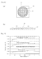
- Figure 1 is a cross-sectional view of a photodiode according to a first exemplary embodiment of the present invention.
- Embedded oxide layer 3 is formed on base substrate 8, and semiconductor layer 1, which is a light absorbing layer, is formed thereon.
- Semiconductor layer 1 is surrounded by oxide film 7.
- Metal electrodes 2 are formed on the surface of semiconductor layer 1. A pairs of metal electrodes 2 is arranged at interval d that is less than wavelength ⁇ of incident light, forming an MSM junction.
- Metal electrodes 2 are embedded into semiconductor layer 1 at distance f that is less than ⁇ /2n, where n is the refractive index of semiconductor layer 1.
- Metal electrodes 2 consist of first metal film 51 that forms a Schottky junction with semiconductor layer 1 and second metal film 52 made of a conductive material that is capable of inducing surface plasmon.
- first metal film 51 and second metal film 52 can also be formed of one type. In this case, metal electrodes 2 have a one-layer configuration.
- a metal electrode formed on the surface of the semiconductor layer covers the light receiving surface of a photodiode, causing a problem of deterioration of light receiving sensitivity.
- photocarriers disadvantageously can not be generated efficiently because the region subject to high optical electric field strength is outside the semiconductor.
- ⁇ /2n which is a distance by which an optical near field can permeate, measured from the surface of the semiconductor layer, and by causing plasmon resonance through radiation of TM wave
- the region having the maximum optical electric field strength and the region of the semiconductor depletion layer, which serves as a light absorbing layer can coincide. Therefore, even a significantly thin light absorbing layer can provide highly efficient sensitivity characteristics.
- the region of a depletion layer having a width of 200 nm or more is formed even under a zero bias. Accordingly, a reduction in the distance between electrodes enables a high-speed and highly sensitive operation of a photodiode even under a low bias voltage.
- drift time between the electrodes required for photocarriers is estimated to be several ps even in the case of a semiconductor material, such as Si, whose photocarrier mobility is about 10 7 cm/s. Even when the thickness of semiconductor layer 1 is set to 1 ⁇ m or less, the drift time can be reduced to 20 ps or less.
- the junction area in the case of an MSM junction means the area measured from one end of the plurality of MSM electrodes to the other end thereof.
- the junction area means the area measured from one end of the plurality of p and n electrodes to the other end thereof.
- the present invention is also applicable to a case in which one metal-semiconductor junction is made of a Schottky barrier type junction and the other metal-semiconductor junction is made of an ohmic junction. Also in this case, if interval d is formed to be less than light wavelength ⁇ and if the electrodes made of a conductive material that is capable of inducing surface plasmon are embedded into the semiconductor at a distance that is less than ⁇ 2n, photodiode characteristics that realize both high efficiency and improved response can be obtained.
- Figure 2 is a cross-sectional view of a photodiode according to a second exemplary embodiment of the present invention.
- semiconductor layer 1 p electrode 9 and n electrode 10 are provided at a predetermined interval, forming a pin junction.
- Metal films 11 made of a conductive material that is capable of inducing surface plasmon are formed on p electrode 9 and n electrode 10 such that metal films 11 are exposed on the surface of semiconductor layer 1.
- Interval d of metal film 11 stacked on p electrode 9 or n electrode 10 is less than wavelength ⁇ of incident light and greater than 1/100 of ⁇ .
- Metal films 11 are embedded into semiconductor layer 1 at distance f that is less than ⁇ /2n measured from the surface of semiconductor layer 1, where n is the refractive index of semiconductor layer 1.
- Metal films 11 that are embedded into the semiconductor layer at distance f that is less than ⁇ /2n measured from the surface of semiconductor layer 1 can, also when applied to the pin photodiode having a lateral electrode structure as shown in Figure 2 , confine optical energy within the region interposed between p electrode 9 and n electrode 10 of semiconductor layer 1 through surface plasmon, producing a locally intensive optical electrical field distribution. It has conventionally been reported that a reduction in the distance between electrodes of a pin photodiode having a lateral electrode structure leads to enhancd response.
- the present invention further by stacking metal films 11 that are capable of inducing surface plasmon on p electrode 9 and n electrode 10 and by embedding metal films 11 at distance f that is less than ⁇ /2n measured from the surface of semiconductor layer 1, which serves as a light absorbing layer, a photodiode having a high speed response and highly efficient sensitivity characteristics can be obtained.
- the conductive material that is capable of inducing surface plasmon is generally made of a material having high conductivity. This significantly contributes to a reduction in impedance in high frequency regions of a downsized photodiode. Thus, a photodiode that realizes both high-speed/high-sensitivity and a high SN ratio in high frequency regions can be obtained.
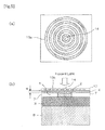
- Figure 3 is a plan view of a surface plasmon resonance structure that functions as a light confining structure that confines incident light within a size (an inner diameter) that is equal to or less than the light wavelength.
- a size an inner diameter
- the incident light can be coupled with surface plasmon that is induced on the surface of metal film 12 and optical energy can be concentrated within micro opening 14 in the form of surface plasmon, and accordingly, transmitted light can be significantly intensified. This effect is called a "surface plasmon enhancement effect.”
- Period means that concave parts and convex parts are alternately and concentrically distributed about micro opening 14.
- Concentration of surface plasmon that is generated on the surface of metal film 12 induces a strong near field on the light emitting side of micro opening 14 via micro opening 14.
- the induced near field is produced by the scattering of the surface plasmon, which is concentrated on the light incident side, at the edge of micro opening 14.
- the surface plasmon includes a component that locally exists as a near field and a component that is scattered and converted to propagating light.
- k SP ⁇ / c ⁇ ⁇ m ⁇ ⁇ d / ⁇ m + ⁇ d
- ⁇ m and ⁇ d are a dielectric constant of metal that produces surface plasmon and a dielectric constant of a dielectric substance adjacent to the metal, respectively.
- the propagation length of surface plasmon is expressed by the following Formula 2.
- L SPP c / ⁇ ⁇ ⁇ m ⁇ + ⁇ d / ⁇ m ⁇ ⁇ 3 / 2 ⁇ ⁇ m ⁇ ⁇ / ⁇ m 2 ⁇
- complex dielectric constant ⁇ m of the metal is expressed as ⁇ m ' + i ⁇ m ".
- Metal film 12 is preferably made up of aluminum, silver, gold or copper or an alloy layer made up of two or more of the elements aluminum, silver, gold and copper. Furthermore, reducing the size of randomly arranged convex and concave parts on the metal surface significantly contributes to a reduction in the propagation loss of the surface plasmon. Therefore, it is also effective to use Ta, Cr, Ti, Zr or the like as a seed layer or to add a trace of an element, such as Nb, to metal film 12 to form an alloy thereof.
- forming at least one metal projection in micro opening 14 allows surface plasmon to excite dipole resonance, allowing a stronger optical near field to be emitted from the outlet of micro opening 14.
- a structure having at least one pair of metal projections 15 opposite to each other intensifies the optical near field in a smaller region.
- metal projections 15 which are intended to produce localized plasmon resonance, are preferably made up of aluminum, silver, gold or copper from the same viewpoint as the viewpoint regarding the optical loss of surface plasmon.
- metal projections 15 may also be an alloy layer including two or more of the elements aluminum, silver, gold and copper.
- Figure 5 is a schematic diagram of a photodiode provided with a surface plasmon resonance structure, wherein (a) and (b) illustrate a plan view and a cross-sectional view, respectively.
- Metal electrode 2 is formed at the location remote from the outlet of micro opening 14 at distance g that is equal to or less than ⁇ /2, and is optically coupled with micro opening 14. Accordingly, both the near field component and the propagating light component at the outlet of micro opening 14 can be localized in the form of plasmon within the region equal to or less than the wavelength on the surface of semiconductor layer 1.
- the intensity and the permeation range vary according to the effect of arrangement of the MSM electrodes, the refractive index of the semiconductor layer and the absorption coefficient of the semiconductor layer.
- This variation enables generation of electron/hole pairs (photocarriers) in a very small region of the semiconductor layer. Therefore, it is possible to make the depletion region in the semiconductor layer formed by the MSM electrodes coincide with the region in which photocarriers are generated by the near field.
- efficient formation of photocarriers and local propagation of the photocarriers can be achieved and a photodiode having high quantum efficiency and high-speed response characteristics can be obtained.
- the junction region of the metal electrodes to generate and sweep photocarriers can be set to a size of 10 ⁇ m 2 or less. As a result, it is possible to reduce the junction electric capacitance to an extremely small level. Therefore, the time constant of the circuit of a photodiode operating at a high frequency can be set to several picoseconds or less and a high frequency operation at more than several tens of GHz is realized.
- a two-dimensional photonic crystalline body has a structure in which photonic crystal holes having micro diameters are arranged in a medium having a high dielectric constant in a staggered pattern or in a lattice pattern.
- a semiconductor most semiconductors have a specific dielectric constant of approximately 12 is typically used for the high dielectric constant medium.
- a photonic band gap occurs when (r/a) is 0.48 and ⁇ ( ⁇ ) ⁇ a)/(2 ⁇ ⁇ c) ⁇ is approximately 0.5, irrespective of the vibration direction of electric field or the direction in which holes extend.
- FIG. 6 is a plan view of a photonic crystal linear defect waveguide manufactured by using a two-dimensional staggered-patterned photonic crystalline structure.
- Photonic crystal linear defect optical waveguide 20 is formed by arranging two two-dimensional staggered-patterned photonic crystalline structures adjacent to each other. A large number of holes 18 are arranged in a staggered pattern in high dielectric constant medium 17.
- One column in which no hole is formed, i.e. , linear defect part 19, is formed in the intermediate region of a large number of holes 18.
- linear defect part 19 functions as an optical waveguide that confines a photoelectric field distribution within a size equal to or less than the wavelength.
- a MSM photodiode is arranged adjacent to such an optical waveguide having high performance in confining light at a distance of half the light wavelength or less. Therefore, optical coupling in a significantly limited region is achieved, and as a result, both high sensitivity and high speed are achieved.
- an optical waveguide having a difference of 5% or more in a refractive index between the core and the clad layer.
- Such a channel type optical waveguide has a structure in which the core is surrounded by a medium having a smaller refractive index than the core, and it is known that light propagates while repeating total reflection caused by the difference in the refractive index between the core and clad layer. In this case, if the difference in the refractive index between the core and the clad layer is large, light is tightly confined in the core and even when the waveguide is sharply bent with a small curvature, light is guided along the waveguide.
- a difference in the refractive index of 5% or more can realize an optical spot diameter of 10 ⁇ m or less. Furthermore, by setting the difference in the refractive index between the core and the clad layer to about 10 to 40%, an optical spot diameter equal to or less than the wavelength can be realized.
- the optical waveguide can be made of a dielectric material, organic compound or semiconductor material.
- a waveguide core is made of semiconductor, such as Si or the like, and if the waveguide core has a refractive index of 3.4 and a cross section of about 0.3 ⁇ m ⁇ 0.3 ⁇ m, and if the core is covered with a clad layer made of SiO 2 having a refractive index of about 1.5, then the mode size of light can be substantially reduced to the size of the waveguide core.
- guided light has a wavelength of about 850 nm, waveguide loss is generated due to optical absorption.
- a difference in the refractive index of 5% or more can be obtained by forming the waveguide core from SiON or the like, which exhibits a light transmitting characteristics showing negligible waveguide loss over a wide wavelength range, and by covering the waveguide core with a clad made of SiO 2 .
- the light confining performance is relatively weakened compared to a case in which a semiconductor core is used, and an optical spot diameter of about 1 to 4 ⁇ m is obtained.
- the light propagation mode is preferably arranged at substantially the same height as the light absorbing layer of the MSM photodiode.
- the group velocity of the guided light can be reduced.
- the MSM junction remote from the waveguide by half the light wavelength or less, optical energy can be more efficiently converted to a photocurrent.
- the ring-type optical resonator structure is preferably disposed above the MSM photodiode or on the lateral side thereof for optical coupling.
- a dielectric film which serves as an optical coupling medium may be provided between the metal electrode and the light confining structure.
- a gas cluster ion beam is preferably used.
- the gas cluster ion beam is a beam obtained by ionizing Ar or reactive gas and gathering it as a cluster made of several hundreds to several thousands of atoms or molecules.
- the gas cluster ion beam when applied to an LSI process, improves yield in a high integration process and provides devices at a low cost.
- the light wavelength used in the present invention ranges over a wide wavelength range that includes visible light, near-infrared light and infrared light.
- a high-speed photodetector for obtaining an electric signal that efficiently generates photocarriers in a wavelength range equal to or less than the wavelength can be obtained by adjusting the sizes of the metal periodic structure that induces surface plasmon resonance, the sizes of a photonic crystal optical waveguide, a channel type optical waveguide and a ring-type optical waveguide that efficiently confine and transmit light and MSM electrodes.
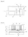
- FIGS 7 and 8 are a cross-sectional view and a plan view of an MSM photodiode according to a first example of the present invention, respectively.
- the MSM type photodiode forms metal-semiconductor-metal (MSM) junctions that are formed on part of semiconductor layer 1 having an insulated surface, such as an SOI (Silicon-on-Insulator). Interval d between metal electrodes 2 is less than wavelength ⁇ of incident light and larger than 1/100 ⁇ . Assuming n is the refractive index of semiconductor layer 1, metal electrodes 2 are embedded into semiconductor layer 1 at distance f that is less than ⁇ /2n measured from the surface of semiconductor layer 1.
- MSM metal-semiconductor-metal
- metal electrode 2 In order to induce surface plasmon, aluminum, silver, gold or copper or an alloy made up of two or more of the elements aluminum, silver, gold and copper is preferably used for metal electrode 2 (or at least second metal film 52).
- a seed film made of Cr, Ta, Ni etc. may also be used in order to form a Schottky junction.
- a seed film made of Ti or the like may be used as an opposite electrode film in order to form an ohmic junction.
- Protection layer 4 made of SiO 2 or the like may also be formed on metal electrodes 2 and may be used as an optical antireflection film.
- Figure 9 shows a comparison of sensitivity characteristics between a case in which Ag electrodes having 30 nm thickness are formed on the surface of a Si semiconductor without being embedded and a case in which the electrodes are embedded at a distance less than ⁇ /2n measured from the surface of the semiconductor.
- the width of the metal electrodes that form the MSM junction and the gap between the electrodes were both set to 100 nm and the embedment depth of the metal electrodes was set to 30 nm. Since the resonance wavelength of surface plasmon was estimated to be 850 nm based on an electromagnetic field calculation, a laser light having a wavelength of 850 nm and 1 mW power was radiated in order to observe photocurrent. It was found that the configuration in which the Ag electrodes are embedded into the Si semiconductor provided a photocurrent that is increased by a factor of hundred or more, and the quantum efficiency was estimated to be about 30% in this case.
- FIG 10 is a cross-sectional view of a photodiode according to a second example of the present invention.
- Schottky electrodes 22 forming a Schottky junction are arranged at interval d on the surface of semiconductor layer 1.
- Schottky electrodes 22 are made of a conductive material that is capable of inducing surface plasmon.
- Opposite electrode layer 23 is formed on the side of base substrate 8 via a depletion layer (semiconductor layer 1) which serves as a light absorbing layer. Interval d of Schottky electrodes 22 is less than light wavelength ⁇ .
- n is the refractive index of semiconductor layer 1
- Schottky electrodes 22 are embedded into semiconductor layer 1 at distance f that is less than ⁇ /2n.
- n+-Si layer that includes a dopant, such as P, with a dopant concentration of 1 ⁇ 10 20 cm -3 or more may be used as opposite electrode layer 23 and an n-Si layer which serves as a light absorbing layer may be used as semiconductor layer 1.
- Semiconductor layer 1 requires epitaxial growth on opposite electrode layer 23. However, if the growth temperature goes beyond 800°C, then the dopant concentration in the light absorbing layer increases due to thermal diffusion of the dopant element, leading to an increase in the depletion voltage and a decrease in the thickness of the depletion layer when the Schottky junction is formed. As a result, low voltage and high speed operation becomes difficult. Therefore, in order to form a thin light absorbing layer on the n+-Si layer, a technique for performing the epitaxial growth at a low temperature of 600°C or less is required.
- the effect of enhancing the photoelectric field by surface plasmon resonance can be generated not only in the horizontal direction between electrodes but also below the electrodes.
- This example is designed such that the enhancement of the photoelectric field by surface plasmon occurs on a Schottky junction interface below the electrodes and thereby the region in which photocarriers are generated coincides with the region in which depletion occurs due to application of a bias voltage.
- Figure 11 is a cross-sectional view of a photodiode according to a third example of the present invention.
- a stack in which metal film 11 is deposited on p electrode 9 or n electrode 10 is disposed on the surface of semiconductor layer 1, forming at least one p-i-n junction.
- Interval d of metal films 11 deposited on p electrode 9 or n electrode 10 is designed to be less than wavelength ⁇ of incident light and to be greater than 1/100 ⁇ .
- Metal film 11 is made of a conductive material that is capable of inducing surface plasmon and metal film 11 is embedded into semiconductor layer 1 at distance f that is less than ⁇ /2n measured from the surface of semiconductor layer 1, where n is the refractive index of semiconductor layer 1.
- Metal film 11 is preferably made up of aluminum, silver, gold or copper or an alloy made up of two or more of the elements aluminum, silver, gold and copper in order to induce surface plasmon.
- trench structures are formed on an SOI (Silicon-on-Insulator) substrate at an interval that is less than light wavelength ⁇ by means of reactive etching using C 4 F 8 and SF 6 .
- SOI Silicon-on-Insulator
- p type and n type polysilicon layers are selectively grown in the trench structures by means of the organic metal vapor-phase epitaxial method. Selective growth is stopped halfway in the trench structures and then aluminum, gold, silver or copper or the like, which are conductive materials that are capable of inducing surface plasmon, is stacked via a seed layer, made of Ti or the like, that improves adhesion to the polysilicon layer.
- An insulating layer made of SiO 2 or the like having a thickness of several nm may be inserted between the conductive material and the i layer (semiconductor layer 1), which serves as a light absorbing layer, in order to limit dark current.
- a quantum efficiency of 50% or more can be achieved even in the case of a Si photodiode by causing enhancement of the optical near field due to surface plasmon to occur in the i layer, which serves as a light absorbing layer and which is interposed between the metal electrodes.
- a quantum efficiency of 90% or more can be achieved in the case of a photodiode in which a Ge layer is grown as an absorbing layer.
- FIG. 12 is a schematic diagram illustrating the configuration of a surface plasmon resonance structure that functions as a light confining structure, wherein (a) is a plan view and (b) is a cross-sectional view.
- Surface plasmon resonance structure 16 has metal film 12 made of Ag etc. which includes a grating configuration (convex/concave section 13) that produces surface plasmon resonance and micro opening 14 that has a diameter of ⁇ or less formed in the center thereof.
- Surface plasmon resonance structure 16 is provided remote from the MSM junction at a distance ⁇ /2 or less and confines incident light within a region equal to or less than the wavelength.
- the period of the grating structure is set such that plasmon resonance occurs for the wavelength of incident light.
- the grating may have a triangular shape or a sinusoidal shape etc. in addition to the rectangular cross section shown in Figure 12(b) . These shapes shift the resonance wavelength to a shorter side as compared to the rectangular cross section.
- a multi-layered structure obtained by periodically arranging two or more types of media whose dielectric functions are different from each other may be used.
- Figure 13 shows a comparison of sensitivity characteristics between a MSM photodiode with a grating configuration that produces plasmon resonance and a MSM photodiode that does not have such a grating configuration.
- the wavelength of incident light was 840 nm and power was 1 mW.
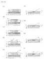
- Figure 14 is a cross-sectional view illustrating the process for manufacturing the photodiode of the present invention.
- an n doped SOI substrate as shown in Figure 14(a) was prepared. Specifically, embedded oxide layer 3 was formed on Si base substrate 8. The resistivity of base substrate 8 was about 1 to 10 ⁇ cm, and doping concentration was about 10 15 to 10 16 cm -3 .
- n type SOI layer (semiconductor layer 1) was subjected to patterning by means of reactive etching that uses a SiNx film as mask 61 and a junction size was defined, as shown in Figure 14(b) .
- a mixture of C 4 F 8 and SF 6 gases was used as a reactive gas.
- in-vapor thermal processing was applied at 1000°C for about 140 minutes to form a mesa structure that was to be a base structure for manufacturing the MSM junction.
- the sides of semiconductor layer 1 were covered with oxide film 7.
- mask 61 was removed by placing mask 61 in hot phosphoric acid at approximately 130°C for approximately one hour, as shown in Figure 14(c) .
- a relatively flat surface can be obtained by optimizing the mesa shape and the thermal oxidation processing.
- a flatness of about several nm can be realized by further applying chemical polishing (CMP).
- a metal layer for forming a Schottky junction was formed on the surface of the manufactured mesa shape.
- groove patterns 62 were formed at interval d on the surface of the semiconductor mesa by means of reactive etching, as shown in Figure 14(d) , and then, metal electrodes 2 were stacked, as shown in Figure 14(e) . More specifically, a metal layer was deposited on semiconductor layer 1 on which groove patterns 62 were formed. Then, a resist pattern (not shown) was formed on groove patterns 62. Then, the metal layer in the region other than the region covered with the resist pattern was removed by etching using Ar gas cluster ions, and metal electrodes 2 were formed in groove patterns 62.
- protection film 4 made of SiO 2 or the like, that shows negligible optical absorption was formed on the MSM photodiode that has been manufactured.
- Protection film 4 serves as a medium layer when the light confining structure, which is formed above the MSM photodiode in the subsequent process, is optically coupled with the MSM photodiode.
- Protection film 4 preferably has a film thickness of ⁇ /n pas or less, where ⁇ is a light wavelength to be detected, and n pas is the refractive index of protection film 4.
- micro opening 14 having a size equal to or less than the wavelength was formed at the center of the manufactured grating configuration (at a location opposite to metal electrodes 2) by means of an etching process using Ar gas cluster ions.
- a mass spectrometer was mounted on the etching apparatus so that the end of etching was detected with an accuracy of 0.1 nm or less.
- Figure 15 is a conceptual diagram of a light confining structure provided with micro projections.
- metal projection 15 that produces dipole resonance through plasmon is provided in micro opening 14, which is formed at the center of convex/concave section 13 that generates surface plasmon resonance.
- Metal projections 15 protrude from the periphery of micro opening 14 into micro opening 14.
- Providing such a metal projection configuration allows optical energy to be confined within a region of 1/4 or less of the light wavelength, making it possible to further reduce the MSM junction that is optically coupled with the region and thereby to obtain a high-speed response of the order of 100 GHz.
- metal projection configuration 15 may also be constituted as at least one pair of metal projections that are opposite to each other. This significantly improves dependency of incident light on polarization.
- elements other than Si that belong to IV group semiconductors such as Ge, Si x Ge 1-x , SiGe, may also be used as the semiconductor layer.
- a III-V group compound particle semiconductor such as GaN, GaAs, GaInAs, GaInP and InP may also be used. These materials are selected based on a wavelength limitation that is determined by the band gap and the absorption coefficient. Excellent photodiode characteristics are obtained in the wavelength range of 400 to 900 nm in the case of Si, 400 to 1400 nm in the case of Ge and 1300 to 1600 nm in the case of InGaAs grown on InP.
- the absorbing layer is formed by making a Ge layer grow with high crystallinity by using a GOI (Germanium On Insulator) substrate instead of an SOI substrate or by using Si substrate according to the metal organic chemical vapor deposition method or the molecular beam epitaxy method.
- a Schottky junction is preferably formed on a NiGe alloy layer, which is made by vapor-depositing Ni or the like on Ge, and by performing annealing at a temperature about 400 to 600°C.
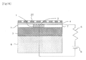
- Figure 16 is a cross-sectional view of a structure in which an MSM photodiode is coupled with a photonic crystal optical waveguide.
- the photonic crystal optical waveguide was formed using an SOI substrate provided with a Si layer having a thickness of 200 to 400 nm.
- a resist for electron beam exposure is applied to the surface of the substrate.
- a resist pattern with cylindrical holes arranged in a matrix pattern was formed using an electron beam exposure apparatus.
- the resist pattern has a hole diameter of 200 to 240 nm with an array pitch of 340 to 380 nm.
- cylindrical holes having the same shape as in the resist mask pattern were formed on the Si surface layer of the SOI substrate by means of the reactive ion etching method, and the resist was then removed.
- Figure 17 is a schematic view illustrating the structure of another photodiode using a photonic crystal optical waveguide of a linear defect type, wherein (a) is a plan view and (b) is a cross-sectional view.
- the MSM photodiode is formed by thinning a Si layer using etching and by making buffer layer 25, which mitigates grating distortion, and selective growth layer 24 made of SiGe or Ge, which serves as a light absorbing layer, grow on the thinned Si layer using metal organic chemical vapor deposition.
- the MSM photodiode is provided at an end of photonic crystal optical waveguide 20.
- the growth end position of the SiGe layer or the Ge layer is controlled by the selective vapor phase epitaxy method so that the distance between the end of the optical waveguide and the MSM electrode is equal to or less than the wavelength in order to allow the MSM photodiode to be optically coupled with photonic crystal linear defect optical waveguide 20.
- Figure 18 shows the dependency of a photocurrent on bias voltage when a laser light having a wavelength of 1330 nm and power of 1 mW is radiated. Although the effect of waveguide loss was present in the photonic crystal linear defect optical waveguide, a quantum efficiency of about 30% was obtained.
- Figure 19 is a cross-sectional view of a structure in which an MSM photodiode is coupled with a channel type optical waveguide.
- the channel type optical waveguide has optical waveguide core 26 that is made of SiON and clad layer 27 that has a refractive index that is largely different from that of optical waveguide core 26.
- the channel type optical waveguide is manufactured as follows. First, as shown in Figure 20(a) , a portion of the Si layer (SOI layer 28) on the SOI substrate on which the optical waveguide is to be formed is etched by means of the reactive etching and the SiO 2 layer which is to become the clad layer is exposed.
- SiON core layer 29 is grown by means of a plasma CVD method using SiH 4 , NH 3 and O 2 so that the difference in the refractive index between the core and clad becomes 5% or more. Then, annealing is conducted at 700 to 1300°C in order to reduce absorption caused by the O-H group or N-H group to improve crystallinity. Next, in order to form the core shape, SiON core layer 29 is etched into a rectangular shape having a width of 0.7 to 4 ⁇ m by means of the reactive etching method.
- a SiO 2 layer which serves as an upper clad layer, is grown to a thickness of about several ⁇ m by means of a plasma CVD method that uses a source gas made of a mixture of TEOS (tetraethylorthosilicate), bubbled with a large amount of Ar, and O 2 .
- a plasma CVD method that uses a source gas made of a mixture of TEOS (tetraethylorthosilicate), bubbled with a large amount of Ar, and O 2 .
- the end face of optical waveguide 29 thus formed was etched at a predetermined angle, and an optical waveguide structure, which is irradiated by the MSM photodiode having a spot diameter of about several ⁇ m, was formed at a distance half the wavelength or less as measured from the position at which the MSM photodiode was formed. Subsequently, the surface the Si layer on the SOI substrate adjacent to the optical waveguide layer was subjected to reactive etching. Thus, the MSM photodiode was manufactured and coupling with light from the SiON optical waveguide was realized.
- Figure 21 shows dependency of a photocurrent on a bias voltage when a laser light having a wavelength of 850 nm and power of 1 mW was radiated.
- a quantum efficiency of about 50% was obtained because a SiO 2 layer was formed between the SiON optical waveguide and the MSM photodiode to improve the efficiency of optical coupling with the MSM photodiode.
- Figure 22 is a conceptual diagram of a photodiode using a channel type optical waveguide of a ring structure.
- the channel type optical waveguide using a Si core is provided with ring-type optical resonator structure 30.
- Optical resonator structure 30 is disposed at a distance of ⁇ /2 or less measured from an MSM photodiode using a light absorbing layer made of a SiGe layer.
- Use of such an optical resonator structure makes it possible to reduce the group velocity of light to 1/6 or less and a quantum efficiency of 70% or more was obtained in the case of a laser light having a wavelength of 1330 nm.
- FIG 23 shows a schematic cross-sectional view of a 40 Gbps (giga-bits per sec) transmission light receiving module on which the MSM photodiode of the present invention is mounted.
- Photodiode 34 is an MSM photodiode that uses a substrate obtained by epitaxial growth of a Ge film on a SOI substrate and that is obtained by forming Au electrodes thereon.
- a light confining structure provided with a metal periodic structure made of Ag or Au is disposed at a distance of ⁇ /2 or less.
- the convex/concave pitch of the metal periodic structure is approximately 1.2 ⁇ m.
- Photodiode 34 is mounted on chip carrier 38 and optically coupled via optical fiber 32 and a lens. Photodiode 34 is also electrically connected to preamplifier IC 37 via electric wiring 36.
- a photodiode that is mounted inside a 40 Gbps optical receiver module uses a side incident type waveguide.
- a planar incident type in which light is incident on a semiconductor surface can not obtain high quantum efficiency if an absorbing layer has a small thickness in order to realize a short charge carrier running time.
- the waveguide type can obtain high quantum efficiency even if the charge carrier running time is short because this type absorbs light in the in-plane direction of the absorbing layer.
- the absorbing layer of the 40 Gbps waveguide type device normally has a thickness of 1 ⁇ m or less, and in this case, the positional coupling tolerance with respect to the optical fiber has to be about ⁇ 1 ⁇ m. This is a large problem both with packaging design and manufacturing cost.
- the photodiode according to the present invention has an effective diameter of 20 ⁇ m, ensuring a coupling tolerance of ⁇ 2 ⁇ m or more.
- optical coupling can be achieved only with simple lens coupling, and this enables a reduction in the cost of a receiver module for optical transmission.
- the 40 Gbps optical receiver module according to the present invention shown in Figure 23 exhibits a minimum receiving sensitivity of -12 dBm in the case of a transmission using a wavelength of 1.55 ⁇ m, and it was confirmed that the 40 Gbps optical receiver module according to the present invention matches, in performance, a 40 Gbps receiver module on which a typical waveguide type photodiode is mounted.
- Figure 24 is a schematic cross-sectional view of an inter-LSI-chip optical interconnection module on which the photodiode of the present invention is mounted.
- An optical signal sent from optical signal input fiber 46 is radiated onto photodiode 34 according to the present invention via concave mirror 48.
- the semiconductor material of photodiode 34 is Si.
- the convex/concave pitch of the metal periodic structure is 600 to 700 nm.
- the photodiode made of Si further makes the optical near field created by the metal periodic structure optically couple with an MSM junction, generating a photocurrent and causing a current that corresponds to the optical signal in LSI 42 via photodiode wiring layer 44.
- a metal periodic structure that causes surface plasmon resonance it is possible to ensure a positional coupling tolerance of ⁇ 1 ⁇ m or more between concave mirror 48 and photodiode 34.
- Photodiode wiring layer 44 is electrically connected to "via holes for photodiode wiring 41" of LSI 42.
- well known methods other than an optical fiber such as a planar optical waveguide, can be used to input an optical signal.
- light concentrating mechanism other than concave mirror 48, such as a convex lens can also be used.
- a preamplifier for amplifying an electric signal may also be disposed immediately after photodiode 34 along the photodiode wiring layer.
- the electric signal sent from LSI 42 is converted to an optical signal by VCSEL (Vertical Cavity Surface Emitting Laser) light source 39 provided with an electric modulation mechanism, via "light source and modulation electric signal via hole 40" and via "light source and modulation electric wiring layer 43".
- the optical signal is reflected by concave mirror 48 and sent to optical signal output fiber 45.
- VCSEL light source 39 provided with the electric modulation mechanism can be replaced by other known mechanisms that modulate light through electricity, such as, a Mach-Zehnder type modulator, which modulates light emitted from an external light source through an electro-optical effect or thermal optical effect.
- a typical inter-LSI-chip interconnection for high-speed operation at 20 GHz or more uses an internally mounted photodiode made of a compound semiconductor material, such as InGaAs or the like, grown on an InP substrate in order to increase the response.
- a compound semiconductor is disadvantageous because it does not fit the manufacturing process of a Si semiconductor device and increases cost.
- the photodiode according to the present invention can reduce the manufacturing cost because it uses Si.
- the illustrated optical interconnection according to the present invention exhibited a high-speed photoelectric conversion operation at approximately 40 GHz.
Applications Claiming Priority (2)
| Application Number | Priority Date | Filing Date | Title |
|---|---|---|---|
| JP2006067594 | 2006-03-13 | ||
| PCT/JP2007/054545 WO2007105593A1 (ja) | 2006-03-13 | 2007-03-08 | フォトダイオード、およびその製造方法、ならびに光通信デバイスおよび光インタコネクションモジュール |
Publications (2)
| Publication Number | Publication Date |
|---|---|
| EP1995793A1 true EP1995793A1 (de) | 2008-11-26 |
| EP1995793A4 EP1995793A4 (de) | 2017-07-05 |
Family
ID=38509419
Family Applications (1)
| Application Number | Title | Priority Date | Filing Date |
|---|---|---|---|
| EP07738036.8A Withdrawn EP1995793A4 (de) | 2006-03-13 | 2007-03-08 | Lichtdiode, verfahren zur herstellung einer derartigen lichtdiode, optische kommunikationsvorrichtung und optisches verbindungsmodul |
Country Status (5)
| Country | Link |
|---|---|
| US (1) | US7800193B2 (de) |
| EP (1) | EP1995793A4 (de) |
| JP (1) | JPWO2007105593A1 (de) |
| CN (1) | CN101438419B (de) |
| WO (1) | WO2007105593A1 (de) |
Cited By (4)
| Publication number | Priority date | Publication date | Assignee | Title |
|---|---|---|---|---|
| FR2940522A1 (fr) * | 2008-12-24 | 2010-06-25 | Commissariat Energie Atomique | Photodetecteur comprenant une region semiconductrice tres mince |
| WO2010126287A1 (en) * | 2009-04-27 | 2010-11-04 | University Of Seoul Industry Cooperation Foundation | Photodiodes with surface plasmon couplers |
| ITVA20090062A1 (it) * | 2009-10-02 | 2011-04-03 | St Microelectronics Srl | Schieramento di fotodiodi per rilevazione di immagini a due terminali uscita di dati multiplati e procedimento di fabbricazione |
| WO2014176596A1 (en) * | 2013-04-26 | 2014-10-30 | Texas Instruments Incorporated | Photodetector array having different photodiode structures |
Families Citing this family (56)
| Publication number | Priority date | Publication date | Assignee | Title |
|---|---|---|---|---|
| US8357980B2 (en) * | 2007-10-15 | 2013-01-22 | Hewlett-Packard Development Company, L.P. | Plasmonic high-speed devices for enhancing the performance of microelectronic devices |
| US8637951B2 (en) | 2008-01-10 | 2014-01-28 | Nec Corporation | Semiconductor light receiving element and optical communication device |
| JP5232981B2 (ja) * | 2008-03-07 | 2013-07-10 | 日本電気株式会社 | SiGeフォトダイオード |
| JP5106487B2 (ja) * | 2008-07-31 | 2012-12-26 | キヤノン株式会社 | 面発光レーザの製造方法及び面発光レーザアレイの製造方法、該製造方法による面発光レーザアレイを備えている光学機器 |
| KR100993894B1 (ko) * | 2008-10-21 | 2010-11-11 | 한국과학기술원 | 랩탑(lap-top) 크기의 근접장 증폭을 이용한 고차 조화파 생성장치 |
| WO2010087785A1 (en) * | 2009-02-02 | 2010-08-05 | Agency For Science, Technology And Research | Thin film solar cell structure |
| US8384012B2 (en) * | 2009-05-11 | 2013-02-26 | Infineon Technologies Ag | Photodiode comprising polarizer |
| EP2430425A4 (de) * | 2009-05-12 | 2015-02-25 | Jean-François Masson | Hochempfindliche plasmonenstrukturen zur verwendung in oberflächenplasmonen-resonanzsensoren und herstellungsverfahren dafür |
| IT1394649B1 (it) * | 2009-06-01 | 2012-07-05 | St Microelectronics Srl | Fotodiodo con contatto schottky sulle pareti di trincee parallele e relativo metodo di fabbricazione |
| JP5829375B2 (ja) * | 2009-06-05 | 2015-12-09 | 日本電気株式会社 | 光学素子とこれを用いた光子発生装置、光発生装置、光記録装置および光検出装置 |
| US8417070B2 (en) * | 2009-09-30 | 2013-04-09 | Intel Corporation | Waveguide coupled surface plasmon polarition photo detector |
| JP5542841B2 (ja) * | 2009-10-15 | 2014-07-09 | 株式会社アドバンテスト | 受光装置、受光装置の製造方法、および受光方法 |
| US8203118B2 (en) * | 2009-12-11 | 2012-06-19 | Honeywell International, Inc. | Ion-trap mass spectrometer driven by a monolithic photodiode array |
| JP5118715B2 (ja) * | 2010-03-11 | 2013-01-16 | 株式会社東芝 | 固体撮像装置 |
| CN101937939A (zh) * | 2010-08-02 | 2011-01-05 | 中国科学院物理研究所 | 一种等离子体薄膜太阳能电池增效方法 |
| CN102456539B (zh) * | 2010-10-19 | 2013-09-11 | 上海华虹Nec电子有限公司 | SiGe监控片的制备方法及采用该片进行监控的方法 |
| US8861909B2 (en) | 2011-02-17 | 2014-10-14 | Cornell University | Polysilicon photodetector, methods and applications |
| CN102881761B (zh) * | 2011-07-15 | 2014-12-10 | 常州光电技术研究所 | Apd红外探测器及其制作方法 |
| CN102290481B (zh) * | 2011-09-01 | 2012-10-31 | 中国科学院半导体研究所 | 具有宽光谱响应的硅探测器结构及其制作方法 |
| CN102324445A (zh) * | 2011-09-22 | 2012-01-18 | 中国科学院苏州纳米技术与纳米仿生研究所 | 具有改良结构的msm光探测器及其制备方法 |
| CN102593132B (zh) * | 2012-02-24 | 2014-04-30 | 天津大学 | 一种基于标准cmos工艺的叠层差分光电探测器 |
| WO2013160968A1 (ja) * | 2012-04-27 | 2013-10-31 | パイオニア株式会社 | フォトダイオード |
| WO2013183178A1 (ja) * | 2012-06-05 | 2013-12-12 | 浜松ホトニクス株式会社 | 光検出器 |
| KR20130141850A (ko) * | 2012-06-18 | 2013-12-27 | 광주과학기술원 | 광학 소자 |
| US10514509B2 (en) * | 2013-01-10 | 2019-12-24 | The Regents Of The University Of Colorado, A Body Corporate | Method and apparatus for optical waveguide-to-semiconductor coupling and optical vias for monolithically integrated electronic and photonic circuits |
| JP5513659B1 (ja) * | 2013-04-26 | 2014-06-04 | 日本電信電話株式会社 | フォトニック結晶光検出器 |
| GB201313592D0 (en) * | 2013-07-30 | 2013-09-11 | Univ St Andrews | Optical modulator with plasmon based coupling |
| US9224882B2 (en) * | 2013-08-02 | 2015-12-29 | Intel Corporation | Low voltage photodetectors |
| WO2015108589A2 (en) | 2013-10-22 | 2015-07-23 | Massachusetts Institute Of Technology | Waveguide formation using cmos fabrication techniques |
| JP6126570B2 (ja) * | 2013-12-13 | 2017-05-10 | 富士フイルム株式会社 | パターン形成方法、電子デバイスの製造方法 |
| US9984917B2 (en) * | 2014-05-21 | 2018-05-29 | Infineon Technologies Ag | Semiconductor device with an interconnect and a method for manufacturing thereof |
| KR102220405B1 (ko) | 2014-07-25 | 2021-02-25 | 삼성전자주식회사 | 광학소자 및 이를 포함한 전자 장치 |
| WO2016132991A1 (ja) * | 2015-02-16 | 2016-08-25 | 国立大学法人静岡大学 | 屈折率測定装置 |
| US9362444B1 (en) * | 2015-03-18 | 2016-06-07 | International Business Machines Corporation | Optoelectronics and CMOS integration on GOI substrate |
| KR101777852B1 (ko) * | 2015-09-24 | 2017-09-13 | 한국표준과학연구원 | 투명기판의 제조방법 및 이를 이용한 표면증강 라만산란 기판의 제조방법 |
| US10983275B2 (en) | 2016-03-21 | 2021-04-20 | The Regents Of The University Of Colorado, A Body Corporate | Method and apparatus for optical waveguide-to-semiconductor coupling for integrated photonic circuits |
| US9749044B1 (en) * | 2016-04-05 | 2017-08-29 | Facebook, Inc. | Luminescent detector for free-space optical communication |
| KR102246017B1 (ko) * | 2017-04-11 | 2021-04-30 | 한국전자통신연구원 | 편광 조절기 |
| CN106972071B (zh) * | 2017-04-26 | 2019-03-01 | 深圳市弘正光电有限公司 | 螺旋盘形分布功能层的光电探测器 |
| JP6944315B2 (ja) * | 2017-09-05 | 2021-10-06 | 浜松ホトニクス株式会社 | 光検出素子 |
| WO2019069585A1 (ja) * | 2017-10-04 | 2019-04-11 | パナソニックIpマネジメント株式会社 | 光デバイス、光電変換装置、および燃料生成装置 |
| CN108333679B (zh) * | 2018-02-11 | 2020-04-21 | 南京邮电大学 | 面向蓝光可见光通信的硅基GaN系光子芯片及制备方法 |
| JP2019169523A (ja) * | 2018-03-22 | 2019-10-03 | 浜松ホトニクス株式会社 | 光検出素子 |
| CN108614314A (zh) * | 2018-05-10 | 2018-10-02 | 江西师范大学 | 一种太阳能全光谱范围完美光吸收器 |
| CN110972505B (zh) * | 2018-09-21 | 2023-10-27 | 深圳市汇顶科技股份有限公司 | 影像感测器及半导体结构 |
| CN109276268A (zh) * | 2018-11-21 | 2019-01-29 | 京东方科技集团股份有限公司 | X射线探测装置及其制造方法 |
| WO2020150938A1 (zh) * | 2019-01-23 | 2020-07-30 | 深圳市汇顶科技股份有限公司 | 光电传感器及其制备方法 |
| JP7169560B2 (ja) * | 2019-03-26 | 2022-11-11 | 株式会社村田製作所 | 共振装置及び共振装置製造方法 |
| FR3095550B1 (fr) * | 2019-04-26 | 2021-05-21 | Commissariat Energie Atomique | Procede de realisation d’un dispositif photo-emetteur et/ou photo-recepteur a grille de separation optique metallique |
| CN110379871B (zh) * | 2019-07-09 | 2021-10-22 | 三明学院 | 一种基于石墨烯的光电探测器 |
| CN112305667B (zh) * | 2019-07-29 | 2021-09-14 | 中国科学院上海微系统与信息技术研究所 | 光波导器件及其制备方法 |
| EP4020036A1 (de) * | 2020-12-23 | 2022-06-29 | EFFECT Photonics B.V. | Umgebungsgeschützte photonische integrierte schaltung |
| CN112769032B (zh) * | 2020-12-31 | 2022-11-01 | 联合微电子中心有限责任公司 | 一种背向集成激光器件及其制造方法 |
| CN113097335B (zh) * | 2021-03-04 | 2023-02-10 | 西安电子科技大学 | 波导耦合等离增强型Ge基红外光电探测器及其制备方法 |
| CN113299775B (zh) * | 2021-05-14 | 2023-02-17 | 北京工业大学 | 一种高速短波通信探测器 |
| CN114566490B (zh) * | 2022-04-15 | 2023-06-27 | 中国电子科技集团公司第十研究所 | 垂直布局msm电容结构及其制作方法 |
Family Cites Families (27)
| Publication number | Priority date | Publication date | Assignee | Title |
|---|---|---|---|---|
| US4555622A (en) | 1982-11-30 | 1985-11-26 | At&T Bell Laboratories | Photodetector having semi-insulating material and a contoured, substantially periodic surface |
| JPS60262473A (ja) | 1984-06-08 | 1985-12-25 | Fujitsu Ltd | 光半導体装置 |
| JPS62205667A (ja) | 1986-03-05 | 1987-09-10 | Nec Corp | 光電変換素子 |
| JPH02214170A (ja) | 1989-02-14 | 1990-08-27 | Mitsubishi Electric Corp | 半導体受光素子 |
| JPH0410476A (ja) * | 1990-04-26 | 1992-01-14 | Fujitsu Ltd | ラテラル型半導体受光素子 |
| JPH0440176A (ja) | 1990-06-06 | 1992-02-10 | Matsushita Electric Ind Co Ltd | テレビジョン特殊効果装置 |
| GB9322246D0 (en) | 1993-10-28 | 1993-12-15 | Hitachi Europ Ltd | Improved metal-semiconductor-metal photodetector |
| US5559359A (en) * | 1994-07-29 | 1996-09-24 | Reyes; Adolfo C. | Microwave integrated circuit passive element structure and method for reducing signal propagation losses |
| US5625729A (en) | 1994-08-12 | 1997-04-29 | Brown; Thomas G. | Optoelectronic device for coupling between an external optical wave and a local optical wave for optical modulators and detectors |
| JP2666888B2 (ja) | 1995-01-23 | 1997-10-22 | 工業技術院長 | 光素子の製造方法 |
| JP2705757B2 (ja) | 1995-01-23 | 1998-01-28 | 工業技術院長 | 受光素子 |
| JPH09270757A (ja) | 1996-04-02 | 1997-10-14 | Toyo Commun Equip Co Ltd | 通信装置の音声増幅回路 |
| US5739561A (en) * | 1996-04-30 | 1998-04-14 | Motorola, Inc. | Light sensitive semiconductor device and method of operation |
| US6236033B1 (en) | 1998-12-09 | 2001-05-22 | Nec Research Institute, Inc. | Enhanced optical transmission apparatus utilizing metal films having apertures and periodic surface topography |
| US6774449B1 (en) * | 1999-09-16 | 2004-08-10 | Matsushita Electric Industrial Co., Ltd. | Semiconductor device and method for fabricating the same |
| FR2803950B1 (fr) * | 2000-01-14 | 2002-03-01 | Centre Nat Rech Scient | Dispositif de photodetection a microresonateur metal- semiconducteur vertical et procede de fabrication de ce dispositif |
| JP2001326420A (ja) | 2000-05-15 | 2001-11-22 | Fuji Xerox Co Ltd | 半導体レーザ、浮上ヘッドおよびディスク装置 |
| US6441298B1 (en) | 2000-08-15 | 2002-08-27 | Nec Research Institute, Inc | Surface-plasmon enhanced photovoltaic device |
| JP2002368253A (ja) | 2001-06-08 | 2002-12-20 | Hitachi Ltd | 光検出器、光記録再生装置、光学顕微鏡 |
| WO2003061020A1 (en) * | 2002-01-04 | 2003-07-24 | Rutgers, The State University Of New Jersey | SCHOTTKY DIODE WITH SILVER LAYER CONTACTING THE ZnO AND MgxZn1-xO FILMS |
| JP3932944B2 (ja) | 2002-03-27 | 2007-06-20 | 日本電気株式会社 | 光学素子およびそれを用いた光ヘッド |
| JP3668779B2 (ja) | 2002-07-25 | 2005-07-06 | 国立大学法人岐阜大学 | 光導波装置 |
| US7061067B2 (en) * | 2003-07-04 | 2006-06-13 | Matsushita Electric Industrial Co., Ltd. | Schottky barrier diode |
| JP2005150291A (ja) | 2003-11-13 | 2005-06-09 | Seiko Epson Corp | 受光素子、光モジュール、及び光伝送装置 |
| EP1737047B1 (de) | 2004-04-05 | 2011-02-23 | NEC Corporation | Fotodiode und herstellungsverfahren dafür |
| JP4399328B2 (ja) | 2004-07-23 | 2010-01-13 | 富士ゼロックス株式会社 | 近接場光出射素子、光ヘッド、および近接場光出射素子の製造方法 |
| US7250666B2 (en) * | 2005-11-15 | 2007-07-31 | International Business Machines Corporation | Schottky barrier diode and method of forming a Schottky barrier diode |
-
2007
- 2007-03-08 JP JP2008505093A patent/JPWO2007105593A1/ja active Pending
- 2007-03-08 CN CN2007800163967A patent/CN101438419B/zh not_active Expired - Fee Related
- 2007-03-08 US US12/282,959 patent/US7800193B2/en not_active Expired - Fee Related
- 2007-03-08 WO PCT/JP2007/054545 patent/WO2007105593A1/ja active Application Filing
- 2007-03-08 EP EP07738036.8A patent/EP1995793A4/de not_active Withdrawn
Non-Patent Citations (1)
| Title |
|---|
| See references of WO2007105593A1 * |
Cited By (10)
| Publication number | Priority date | Publication date | Assignee | Title |
|---|---|---|---|---|
| FR2940522A1 (fr) * | 2008-12-24 | 2010-06-25 | Commissariat Energie Atomique | Photodetecteur comprenant une region semiconductrice tres mince |
| WO2010072942A1 (fr) * | 2008-12-24 | 2010-07-01 | Commissariat A L'energie Atomique Et Aux Energies Alternatives | Photodetecteur comprenant une region semiconductrice tres mince |
| US8698207B2 (en) | 2008-12-24 | 2014-04-15 | Commissariat A L'energie Atomique Et Aux Energies Alternatives | Photodetector having a very thin semiconducting region |
| WO2010126287A1 (en) * | 2009-04-27 | 2010-11-04 | University Of Seoul Industry Cooperation Foundation | Photodiodes with surface plasmon couplers |
| US8247881B2 (en) | 2009-04-27 | 2012-08-21 | University Of Seoul Industry Cooperation Foundation | Photodiodes with surface plasmon couplers |
| KR101322364B1 (ko) * | 2009-04-27 | 2013-10-28 | 서울시립대학교 산학협력단 | 표면 플라스몬 커플러를 가지는 포토다이오드 |
| ITVA20090062A1 (it) * | 2009-10-02 | 2011-04-03 | St Microelectronics Srl | Schieramento di fotodiodi per rilevazione di immagini a due terminali uscita di dati multiplati e procedimento di fabbricazione |
| US8264019B2 (en) | 2009-10-02 | 2012-09-11 | Stmicroelectronics S.R.L. | Multiplexed output two terminal photodiode array for imaging applications and related fabrication process |
| US8338219B2 (en) | 2009-10-02 | 2012-12-25 | Stmicroelectronics S.R.L. | Multiplexed output two terminal photodiode array for imaging applications and related fabrication process |
| WO2014176596A1 (en) * | 2013-04-26 | 2014-10-30 | Texas Instruments Incorporated | Photodetector array having different photodiode structures |
Also Published As
| Publication number | Publication date |
|---|---|
| JPWO2007105593A1 (ja) | 2009-07-30 |
| CN101438419B (zh) | 2012-02-22 |
| US7800193B2 (en) | 2010-09-21 |
| US20090134486A1 (en) | 2009-05-28 |
| EP1995793A4 (de) | 2017-07-05 |
| WO2007105593A1 (ja) | 2007-09-20 |
| CN101438419A (zh) | 2009-05-20 |
Similar Documents
| Publication | Publication Date | Title |
|---|---|---|
| US7800193B2 (en) | Photodiode, method for manufacturing such photodiode, optical communication device and optical interconnection module | |
| US10468543B2 (en) | Microstructure enhanced absorption photosensitive devices | |
| JP5282887B2 (ja) | フォトダイオード、光通信デバイスおよび光インタコネクションモジュール | |
| US8467637B2 (en) | Waveguide path coupling-type photodiode | |
| EP1737047B1 (de) | Fotodiode und herstellungsverfahren dafür | |
| US10622498B2 (en) | Microstructure enhanced absorption photosensitive devices | |
| US8637951B2 (en) | Semiconductor light receiving element and optical communication device | |
| JP4835837B2 (ja) | フォトダイオードとその製造方法 | |
| JP5232981B2 (ja) | SiGeフォトダイオード | |
| US20180102442A1 (en) | Microstructure enhanced absorption photosensitive devices | |
| WO2019089437A1 (en) | Microstructure enhanced absorption photosensitive devices | |
| US20190019903A1 (en) | SILICON WAVEGUIDE INTEGRATED WITH SILICON-GERMANIUM (Si-Ge) AVALANCHE PHOTODIODE DETECTOR | |
| US20220102563A1 (en) | Microstructure enhanced absorption photosensitive devices | |
| WO2013146406A1 (ja) | 導波路結合msm型フォトダイオード | |
| CN117650190A (zh) | 一种适用于非偏振光的等离激元电极光电探测器 |
Legal Events
| Date | Code | Title | Description |
|---|---|---|---|
| PUAI | Public reference made under article 153(3) epc to a published international application that has entered the european phase |
Free format text: ORIGINAL CODE: 0009012 |
|
| 17P | Request for examination filed |
Effective date: 20080910 |
|
| AK | Designated contracting states |
Kind code of ref document: A1 Designated state(s): BE DE FR |
|
| RBV | Designated contracting states (corrected) |
Designated state(s): BE DE FR |
|
| DAX | Request for extension of the european patent (deleted) | ||
| RA4 | Supplementary search report drawn up and despatched (corrected) |
Effective date: 20170608 |
|
| RIC1 | Information provided on ipc code assigned before grant |
Ipc: H01L 31/108 20060101AFI20170601BHEP |
|
| 17Q | First examination report despatched |
Effective date: 20170616 |
|
| STAA | Information on the status of an ep patent application or granted ep patent |
Free format text: STATUS: THE APPLICATION IS DEEMED TO BE WITHDRAWN |
|
| 18D | Application deemed to be withdrawn |
Effective date: 20171027 |