EP1978339B1 - Infrarotabsorber und thermischer infrarotdetektor - Google Patents
Infrarotabsorber und thermischer infrarotdetektor Download PDFInfo
- Publication number
- EP1978339B1 EP1978339B1 EP07707332.8A EP07707332A EP1978339B1 EP 1978339 B1 EP1978339 B1 EP 1978339B1 EP 07707332 A EP07707332 A EP 07707332A EP 1978339 B1 EP1978339 B1 EP 1978339B1
- Authority
- EP
- European Patent Office
- Prior art keywords
- infrared ray
- layer
- wavelength range
- over
- tin
- Prior art date
- Legal status (The legal status is an assumption and is not a legal conclusion. Google has not performed a legal analysis and makes no representation as to the accuracy of the status listed.)
- Ceased
Links
Images


Classifications
-
- G—PHYSICS
- G01—MEASURING; TESTING
- G01J—MEASUREMENT OF INTENSITY, VELOCITY, SPECTRAL CONTENT, POLARISATION, PHASE OR PULSE CHARACTERISTICS OF INFRARED, VISIBLE OR ULTRAVIOLET LIGHT; COLORIMETRY; RADIATION PYROMETRY
- G01J5/00—Radiation pyrometry, e.g. infrared or optical thermometry
- G01J5/02—Constructional details
-
- H—ELECTRICITY
- H10—SEMICONDUCTOR DEVICES; ELECTRIC SOLID-STATE DEVICES NOT OTHERWISE PROVIDED FOR
- H10F—INORGANIC SEMICONDUCTOR DEVICES SENSITIVE TO INFRARED RADIATION, LIGHT, ELECTROMAGNETIC RADIATION OF SHORTER WAVELENGTH OR CORPUSCULAR RADIATION
- H10F39/00—Integrated devices, or assemblies of multiple devices, comprising at least one element covered by group H10F30/00, e.g. radiation detectors comprising photodiode arrays
- H10F39/10—Integrated devices
- H10F39/12—Image sensors
- H10F39/191—Photoconductor image sensors
- H10F39/193—Infrared image sensors
-
- G—PHYSICS
- G01—MEASURING; TESTING
- G01J—MEASUREMENT OF INTENSITY, VELOCITY, SPECTRAL CONTENT, POLARISATION, PHASE OR PULSE CHARACTERISTICS OF INFRARED, VISIBLE OR ULTRAVIOLET LIGHT; COLORIMETRY; RADIATION PYROMETRY
- G01J5/00—Radiation pyrometry, e.g. infrared or optical thermometry
- G01J5/02—Constructional details
- G01J5/04—Casings
- G01J5/046—Materials; Selection of thermal materials
-
- G—PHYSICS
- G01—MEASURING; TESTING
- G01J—MEASUREMENT OF INTENSITY, VELOCITY, SPECTRAL CONTENT, POLARISATION, PHASE OR PULSE CHARACTERISTICS OF INFRARED, VISIBLE OR ULTRAVIOLET LIGHT; COLORIMETRY; RADIATION PYROMETRY
- G01J5/00—Radiation pyrometry, e.g. infrared or optical thermometry
- G01J5/02—Constructional details
- G01J5/08—Optical arrangements
- G01J5/0853—Optical arrangements having infrared absorbers other than the usual absorber layers deposited on infrared detectors like bolometers, wherein the heat propagation between the absorber and the detecting element occurs within a solid
-
- G—PHYSICS
- G01—MEASURING; TESTING
- G01J—MEASUREMENT OF INTENSITY, VELOCITY, SPECTRAL CONTENT, POLARISATION, PHASE OR PULSE CHARACTERISTICS OF INFRARED, VISIBLE OR ULTRAVIOLET LIGHT; COLORIMETRY; RADIATION PYROMETRY
- G01J5/00—Radiation pyrometry, e.g. infrared or optical thermometry
- G01J5/10—Radiation pyrometry, e.g. infrared or optical thermometry using electric radiation detectors
- G01J5/12—Radiation pyrometry, e.g. infrared or optical thermometry using electric radiation detectors using thermoelectric elements, e.g. thermocouples
Definitions
- the present invention relates to an infrared ray absorber and a thermal infrared ray detector.
- a conventional thermal infrared ray detector includes, for example, that described in Patent Document 1 or 2.
- Patent Document 1 has disclosed a pyroelectric infrared ray solid-state image pickup device.
- An infrared ray absorbing film used in the device has a laminated structure composed of an organic layer sensitive in a wide range of infrared ray and an SiO 2 layer high in absorption rate in the vicinity of a wavelength of 10 ⁇ m.
- Patent Document 2 has disclosed a thermal infrared ray sensor.
- the sensor has a multi-structured infrared ray absorbing film containing a metal thin film at the lowermost layer.
- the metal thin film is greater in reflection rate of infrared ray than in transmission rate of infrared ray, attempting to increase the absorption rate of infrared ray on other layers by allowing infrared ray in an attempt to transmit through the other layers to reflect on the metal thin film.
- JP 2000 321125 relates to an infrared sensor element.
- an infrared ray absorber is formed on a substrate to keep a mechanical strength. Then, in order to attain an accurate detection of heat generated by the infrared ray absorber, a substrate portion of a detecting region is removed by wet etching or others (membrane structure: refer to Patent Document 2, for example).
- a substrate portion of a detecting region is removed by wet etching or others (membrane structure: refer to Patent Document 2, for example).
- the organic layer is lower in resistance to wet etching, thus posing a difficulty in processing a substrate.
- Patent Document 2 has not described anything about the detection capability over a wider wavelength range.
- the present invention has been made in view of the above problem, an object of which is to provide an infrared ray absorber in which a substrate can be easily subjected to wet etching, and infrared ray can be absorbed over a wider wavelength range at a higher efficiency and a thermal infrared ray detector.
- a thermal infrared ray detector is defined in claim 1.
- TiN is characterized in that it is higher in absorption rate of infrared ray over a wavelength range shorter than 8 ⁇ m than other inorganic materials, while higher in reflection rate of infrared ray over a wavelength range longer than 8 ⁇ m. Therefore, if a second layer excellent in absorption rate of infrared ray longer than 8 ⁇ m in a wavelength range is laminated on a first layer (TiN layer), infrared ray over a range wavelength lower in absorption rate on the TiN layer can be favorably absorbed on the second layer, and also infrared ray in an attempt to transmit the second layer can be reflected on a boundary surface of the TiN layer and returned to the second layer.
- the above-described infrared ray absorber is provided on a first layer containing TiN with a second layer containing an Si based compound high in absorption rate of infrared ray over a wavelength range longer than 8 ⁇ m. Thereby, it is possible to efficiently absorb infrared ray over a wider wavelength range.
- the first layer containing TiN mainly absorbs infrared ray over a wavelength range shorter than 8 ⁇ m and also reflects infrared ray longer than 8 ⁇ m in a wavelength range toward the second layer.
- one layer is provided with both a function of absorbing infrared ray over a certain range of wavelength and that of reflecting infrared ray over other ranges of wavelength to other layers, thereby making it possible to efficiently absorb infrared ray over a wider wavelength range by the use of a smaller number of layers than a case where a layer mainly for reflection is provided.
- the second layer contains at least one of the materials in claim 1 as an Si based compound.
- SiC and SiN are in particular high in resistance to wet etching as compared with other Si based compounds, and the infrared ray absorber can be, therefore, used to more easily manufacture a membrane structure.
- the second layer is thicker than the first layer.
- TiN constituting the first layer is extremely small in transmission rate of infrared ray when the thickness exceeds a certain value, and hardly varies in absorption rate or reflection rate even if the thickness is allowed to change.
- an Si based compound constituting the second layer will be increased in absorption rate as it becomes thicker. Therefore, the second layer containing an Si based compound is made thicker than the first layer containing Ti, by which infrared ray longer than 8 ⁇ m in a wavelength range can be more efficiently absorbed.
- thermal infrared ray detector is provided that a substrate is easily subjected to wet etching and infrared ray can be efficiently detected over a wider wavelength range.
- an infrared ray absorber in which a substrate is easily subjected to wet etching and infrared ray can be absorbed efficiently over a wider wavelength range and a thermal infrared ray detector.
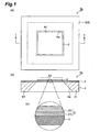
- Fig. 1(a) is a plan view showing Embodiment 1 of a thermal infrared ray detector provided with the infrared ray absorber of the present invention.
- Fig. 1(b) is a side sectional view showing a cross section taken along the line I-I given in Fig. 1(a) .
- Fig. 1(c) is an enlarged sectional view in which Fig. 1(b) is partially enlarged.
- a thermal infrared ray detector 1a of the present embodiment is a thermal infrared ray detector, which is formed by using so-called bulk micromachine technology and provided with an infrared ray absorbing film 2, a thermopile forming film 3 and a silicon (Si) substrate 4.
- the silicon substrate 4 is formed in a rectangular flat shape and has a frame portion 41 provided along the outer periphery.
- An opening 4a corresponding in size to the infrared ray detecting region A1 is formed near the center enclosed by the frame portion 41.
- a thermopile forming film 3 and an infrared ray absorbing film 2, which will be described later, are given as a membrane structure.
- the opening 4a is preferably formed by selective wet etching employed in the silicon substrate 4.
- the thermopile forming film 3 is a thermoelectric converter for converting heat from an infrared ray absorbing film 2 to be described later to an electrical quantity (electrical voltage, current and the like).
- the thermopile forming film 3 is provided on the silicon substrate 4 so as to cover the opening 4a and constituted in such a manner that a plurality of thermoelements are arranged two dimensionally.
- Hot junctions (thermocouples) of the plurality of thermoelements are respectively arranged inside an infrared ray detecting region A1, and cold junctions are arranged on the frame portion 41.
- the infrared ray absorbing film 2 is an infrared ray absorber in the present embodiment and provided at the infrared ray detecting region A1 on the thermopile forming film 3.
- the infrared ray absorbing film 2 is provided with a first layer 21 mainly containing TiN and a second layer 22 mainly containing an Si based compound such as SiC, SiN, SiO 2 , Si 3 N 4 or SiON and provided on the first layer 21, converting energy of infrared ray made incident from the second layer 22 to heat.
- the second layer 22 is formed so as to be thicker than the first layer 21.
- the second layer 22 mainly contains at least one of SiC and SiN as an Si based compound. Further, where the second layer 22 contains mainly SiO x N y (0 ⁇ X ⁇ 2, 0 ⁇ Y ⁇ 1) and a composition ratio of oxygen atoms X/(X + Y) is in a range of 0.4 or more to 0.8 or less, the light transmission rate is improved and the moisture resistance is also increased, which is preferable.
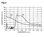
- Fig. 2 is a graph showing infrared ray absorption characteristics of TiN and SiC (absorption rate according to incident wavelength).
- the graph G1 shows the absorption characteristics of TiN
- the graph G2 shows the absorption characteristics of SiC.
- TiN is higher in absorption rate over a relatively short wavelength range, that is, over a wavelength range shorter than 8 ⁇ m, for example.
- SiC is higher in absorption rate over a relatively long wavelength range, that is, over a wavelength range from 8 ⁇ m to 14 ⁇ m, for example.
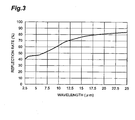
- Fig. 3 is a graph showing infrared ray reflection characteristics of TiN (reflection rate according to incident wavelength). As shown in Fig. 3 , TiN is higher in reflection rate over a relatively long wavelength range, that is, over a wavelength range longer than 8 ⁇ m, for example.
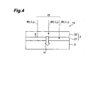
- Fig. 4 is a drawing for explaining operations of the thermal infrared ray detector 1 a in the present embodiment.
- Fig. 4 shows a side cross section at a part corresponding to the infrared ray detecting region A 1 in the thermal infrared ray detector 1a.
- Infrared ray IR made incident into the infrared ray detecting region A1 of the thermal infrared ray detector 1a is made incident into an infrared ray absorbing film 2 from a second layer 22. Then, among the infrared ray IR, a wavelength component, which is relatively short in wavelength (a component whose wavelength will not exceed, for example, 8 ⁇ m) IR ( ⁇ 1 ) is transmitted through the second layer 22, mainly absorbed by the first layer 21 and converted to heat H. Further, among infrared ray IR, a wavelength component relatively long in wavelength (for example, a component whose wavelength will exceed, for example, 8 ⁇ m) IR ( ⁇ 2 ) is absorbed by the second layer 22 and converted to heat H.
- thermopile forming film 3 a part of the wavelength component IR ( ⁇ 2) arrives at a boundary surface between the first layer 21 and the second layer 22 in an attempt to transmit the second layer 22. However, it is reflected on the boundary surface due to a high reflection rate of TiN contained in the first layer 21 and finally absorbed by the second layer 22. The thus generated heat H passes through the first layer 21 containing TiN higher in thermal conductivity and arrives at a thermopile forming film 3. Then, voltage depending on the magnitude of heat H is generated in the thermopile forming film 3.
- TiN is characteristically higher in absorption rate of infrared ray IR ( ⁇ 1 ) over a wavelength range shorter than 8 ⁇ m than other inorganic materials, while higher in reflection rate of infrared ray IR ( ⁇ 2 ) over a wavelength range longer than 8 ⁇ m.
- infrared ray IR ( ⁇ 2 ) over a wavelength range longer than 8 ⁇ m is laminated on the first layer 21, infrared ray IR ( ⁇ 2 ) over a wavelength range, which is less likely to be absorbed by the first layer 21, can be favorably absorbed by the second layer 22.
- infrared ray IR ( ⁇ 2 ) in an attempt to transmit the second layer 22 can also be reflected on the boundary surface of the first layer 21, returned to the second layer 22 and absorbed by the second layer 22.
- the infrared ray absorbing film 2 of the present embodiment is provided on the first layer 21 containing TiN with the second layer 22 containing an Si based compound higher in absorption rate of infrared ray IR ( ⁇ 2 ) over a wavelength range longer than 8 ⁇ m.
- the wavelength from 8 ⁇ m to 14 ⁇ m are a wavelength range often used in determining radiation temperatures and detecting human bodys. Therefore, an Si based compound (SiC in particular), which is high in absorption rate of infrared ray over the above-mentioned wavelength range, is mainly contained in the second layer 22, thereby the above determination can be made accurately.
- an Si based compound (SiC in particular) is high in transmission rate of infrared ray in the vicinity of the wavelength 5 ⁇ m at which TiN is high in absorption rate thereof. Therefore, the second layer 22 contains mainly an Si based compound, by which infrared ray IR ( ⁇ 1 ) over the above-described wavelength range can be efficiently made incident into the first layer 21 to increase an absorption efficiency to a greater extent. Still further, since TiN is low in transmission rate of infrared ray, even when it is formed relatively thin (transmission rate of 10% or less at the thickness of 4000 ⁇ , for example), TiN is used in the first layer 21, thus making it possible to reduce a film-forming time of the first layer 21.
- the first layer 21 contains mainly TiN, by which it is possible to transmit heat generated on the first layer 21 and the second layer 22 to the thermopile forming film 3 without loss of the heat by radiation or the like and also increase a response speed of the thermal infrared ray detector 1a.
- Fig. 5 is a graph showing infrared ray absorption characteristics of the infrared ray absorbing film 2 of the present embodiment as a whole (absorption rate according to incident wavelength).
- the infrared ray absorbing film 2 is able to efficiently absorb infrared ray both over a wavelength range longer than 8 ⁇ m (in the vicinity of 8 ⁇ m to 18 ⁇ m, in particular) and a wavelength range shorter than 8 ⁇ m (in the vicinity of 4 ⁇ m, in particular).
- the absorption rate over a wavelength range longer than 8 ⁇ m is higher than the absorption rate of a single layer of SiC given in Fig. 2 .
- infrared ray over the above-described wavelength range is considered to be more efficiently absorbed by the second layer 22 due to the reflection on the boundary surface between the first layer 21 (TiN) and the second layer 22 (SiC).
- the first layer 21 containing TiN absorbs mainly infrared ray IR ( ⁇ 1 ) over a wavelength range shorter than 8 ⁇ m and also reflects toward the second layer 22 infrared ray IR ( ⁇ 2 ) over a wavelength range longer than 8 ⁇ m.
- one layer is provided with both a function of absorbing infrared ray IR ( ⁇ 1 ) over a certain range of wavelength and that of reflecting infrared ray IR ( ⁇ 2 ) over other ranges of wavelength to the other layer (second layer 22), thereby making it possible to efficiently absorb infrared ray over a wider wavelength range by the use of a smaller number of layers than a case where a layer mainly for reflection is provided.
- the infrared ray absorbing film 2 of the present embodiment it is possible to easily manufacture a membrane structure at which a substrate portion of the infrared ray detecting region A1 (a part corresponding to an opening 4a) is removed.
- the second layer 22 contains mainly SiC and SiN as an Si based compound, SiC and SiN are higher in resistance to wet etching as compared with other Si based compounds, thereby a membrane structure can be manufactured more easily, which is more preferable.
- the second layer 22 is thicker than the first layer 21.
- TiN which constitutes the first layer 21, is extremely small in transmission rate of infrared ray, when the thickness exceeds a certain value, and hardly varies in absorption rate or reflection rate according to a change in thickness.
- an Si based compound which constitutes the second layer 22, will be increased in absorption rate as it is made thicker.
- the second layer 22 is made thicker than the first layer 21, thus making it possible to more efficiently absorb infrared ray IR ( ⁇ 2 ) over a wavelength range longer than 8 ⁇ m.
- the second layer 22 of the present embodiment has actions different from those of a general Si based compound film used only for protecting an infrared ray absorbing film (for example, SiO 2 film). Specifically, a film used only for protecting an infrared ray absorbing film is in general thinner than the infrared ray absorbing film.
- the second layer 22 of the present embodiment is, as described above, preferred to be thicker than the first layer 21 because it partially constitutes the infrared ray absorbing film 2 for efficiently absorbing infrared ray.
- the thickness of the first layer 21 is preferably in a range of 2500 ⁇ to 10000 ⁇ .
- the first layer 21 is 2500A or higher in thickness, it is decreased in transmission rate of infrared ray IR ( ⁇ 1 ) and IR ( ⁇ 2 ), thus making it possible to sufficiently secure the absorption rate and the reflection rate. Therefore, it is able to efficiently provide a function of absorbing infrared ray IR ( ⁇ 1 ) over a wavelength range shorter than 8 ⁇ m, and also a function of reflecting infrared ray IR ( ⁇ 2 ) over a wavelength range longer than 8 ⁇ m.
- the first layer 21 exceeds 10000 ⁇ in thickness, it tends to be saturated in absorption rate of infrared ray IR ( ⁇ 1 ) over a wavelength range shorter than 8 ⁇ m (the absorption rate hardly increases with an increase in thickness).
- the first layer 21 is set to be 10000 ⁇ or less in thickness, by which the first layer 21 can be reduced in layer-forming time.
- the thickness of the second layer 22 is preferably in a range of 10000 ⁇ to 25000 ⁇ . Where the second layer 22 is 10000 ⁇ or higher in thickness, it can be made possible to sufficiently secure the absorption rate of infrared ray IR ( ⁇ 2 ). Still further, where the second layer 22 exceeds 25000 ⁇ in thickness, it is increased in absorption rate of infrared ray IR ( ⁇ 2 ) in the vicinity of 100% and consequently saturated. Thus, the second layer 22 is 25000 ⁇ or less in thickness, by which the second layer 22 can be reduced in layer-forming time.
- the second layer 22 is preferably thicker than the first layer 21.
- An Si based compound, which constitutes the second layer 22, is thicker in thickness at which the absorption rate is saturated than TiN, which constitutes the first layer 21 (an Si based compound: 25000 ⁇ , TiN: 10000 A). Therefore, the second layer 22 is made thicker than the first layer 21, thereby infrared ray can be absorbed more efficiently.
- a ratio of the thickness of the second layer 22, t 2 , to that of the first layer 21, t 1 , (t 2 /t 1 ) is preferably in a range of 1 to 10 and an optimal ratio is 3.
- Fig. 6 (a) is a plan view showing Embodiment 2 of a thermal infrared ray detector provided with the infrared ray absorber of the present invention.
- Fig. 6 (b) is a side sectional view showing a cross section taken along the line II-II given in Fig. 6 (a) .
- Fig. 6 (c) is an enlarged sectional view in which Fig. 6 (b) is partially enlarged.
- a thermal infrared ray detector 1b of the present embodiment is a thermal infrared ray detector, which is formed by using so-called surface micromachine technology and provided with an infrared ray absorbing film 5, a thermopile forming film 6 and a silicon (Si) substrate 7.
- the silicon substrate 7 is formed in a rectangular flat shape and provided with a rectangular cavity 7a at a part corresponding to an infrared ray detecting region A2 on the surface.
- the cavity 7a is favorably formed by wet etching.
- the thermopile forming film 6 is a thermoelectric converter for converting heat from the infrared ray absorbing film 5 to an electrical quantity (electrical voltage, current and the like).
- the thermopile forming film 6 is provided on the silicon substrate 7 so as to cover the cavity 7a and constituted in such a manner that a plurality of thermoelements are arranged two dimensionally.
- Hot junctions (thermocouples) of the plurality of thermoelements are respectively arranged inside an infrared ray detecting region A2, and cold junctions are arranged on the surface of the silicon substrate 7 excluding the cavity 7a.
- the infrared ray absorbing film 5 is an infrared ray absorber in the present embodiment and provided at the infrared ray detecting region A2 on the thermopile forming film 6. Since a cavity 7a is formed on the surface of the silicon substrate 7 corresponding to the infrared ray detecting region A2, the infrared ray absorbing film 5 constitutes a membrane structure, together with the thermopile forming film 6.
- the infrared ray absorbing film 5 is provided with a first layer 51 mainly containing TiN and a second layer 52 mainly containing an Si based compound such as SiC, SiN, SiO 2 , Si 3 N 4 or SiON and provided on the first layer 51, converting energy of infrared ray made incident from the second layer 52 to heat.
- the second layer 52 preferably contains at least one of SiC and SiN, as an Si based compound or may contain mainly SiO x N y (0 ⁇ X ⁇ 2, 0 ⁇ Y ⁇ 1).
- holes 5a and 6a which penetrate through in a thickness direction, are respectively formed on the infrared ray absorbing film 5 and the thermopile forming film 6.
- These holes 5a and 6a are holes for allowing etchant for forming the cavity 7a on the silicon substrate 7 to enter into the back of the thermopile forming film 6, and a plurality of the holes are formed on the infrared ray absorbing film 5 and the thermopile forming film 6.
- the holes 5a and 6a also act in such a manner that the thermopile forming film 6 will not move due to a change in pressure of the cavity 7a, upon operation as an infrared ray detector, in particular upon nitrogen containment.
- the thermal infrared ray detector 1b of the present embodiment is able to provide effects similar to those of the thermal infrared ray detector 1a of Embodiment 1.
- the thermal infrared ray absorber and the thermal infrared ray detector of the present invention shall not be limited to the above-described embodiments but can be applied to various modifications.
- the thermal infrared ray detector of each of the above-described embodiments is constituted so as to give a thermoelectric power type equipped with a thermopile as a thermoelectric converter.
- it may be constituted so as to give, for example, a pyroelectric type equipped with a LiTaO 3 film and a PZT film or a resistance type equipped with a thermistor or a bolometer.
Landscapes
- Physics & Mathematics (AREA)
- General Physics & Mathematics (AREA)
- Spectroscopy & Molecular Physics (AREA)
- Photometry And Measurement Of Optical Pulse Characteristics (AREA)
- Laminated Bodies (AREA)
Claims (2)
- Thermischer Infrarotstrahlendetektor, der umfasst:einen Infrarotstrahlenabsorber (2, 5), undeinen thermoelektrischen Wandler (3, 6) zum Wandeln von Wärme aus dem Infrarotstrahlenabsorber (2) zu einer elektrischen Größe,wobei der Infrarotstrahlenabsorber (2, 5) umfasst:eine erste Schicht (21, 51) aus TiN, undeine zweite Schicht (22, 52), die hauptsächlich eine Si-basierte Verbindung enthält und auf der ersten Schicht (21, 51) vorgesehen ist, um die Energie von auf die zweite Schicht (22, 52) einfallenden Infrarotstrahlen zu Wärme zu wandeln, wobei die zweite Schicht (22, 52) zwischen einer Infrarotstrahlen-Einfallsseite und der ersten Schicht (21, 51) eingeschlossen ist,dadurch gekennzeichnet, dassder Infrarotstrahlenabsorber (2, 5) auf dem thermoelektrischen Wandler (3, 6) vorgesehen ist und zusammen mit dem thermoelektrischen Wandler (3, 6) einen Membranenaufbau bildet,die zweite Schicht dicker als die erste Schicht ist, wobei das Verhältnis der Dicke der zweiten Schicht (22) zu derjenigen der ersten Schicht (21) im Bereich von 1 bis 10 liegt,die zweite Schicht (22, 52) wenigstens eines von SiC, SiN, SiO2, Si3N4 und SiON als die Si-basierte Verbindung enthält, unddie zweite Schicht (22, 52) vor allem SiOxNy enthält, wobei das Zusammensetzungsverhältnis der Sauerstoffatome X/(X+Y) im Bereich von 0,4 bis 0,8 liegt, wobei 0 < X ≤ 2 und 0 ≤ Y < 1.
- Thermischer Infrarotstrahlendetektor nach Anspruch 1, wobei die Dicke der ersten Schicht (21) im Bereich von 2500 A bis 10000 Å liegt, und
die Dicke der zweiten Schicht (22) im Bereich von 10000 Å bis 25000 Å liegt.
Applications Claiming Priority (2)
| Application Number | Priority Date | Filing Date | Title |
|---|---|---|---|
| JP2006016733A JP5283825B2 (ja) | 2006-01-25 | 2006-01-25 | 熱型赤外線検出器 |
| PCT/JP2007/051085 WO2007086424A1 (ja) | 2006-01-25 | 2007-01-24 | 赤外線吸収体および熱型赤外線検出器 |
Publications (3)
| Publication Number | Publication Date |
|---|---|
| EP1978339A1 EP1978339A1 (de) | 2008-10-08 |
| EP1978339A4 EP1978339A4 (de) | 2012-05-09 |
| EP1978339B1 true EP1978339B1 (de) | 2015-01-07 |
Family
ID=38309213
Family Applications (1)
| Application Number | Title | Priority Date | Filing Date |
|---|---|---|---|
| EP07707332.8A Ceased EP1978339B1 (de) | 2006-01-25 | 2007-01-24 | Infrarotabsorber und thermischer infrarotdetektor |
Country Status (7)
| Country | Link |
|---|---|
| US (1) | US8664510B2 (de) |
| EP (1) | EP1978339B1 (de) |
| JP (1) | JP5283825B2 (de) |
| KR (1) | KR101427431B1 (de) |
| CN (1) | CN101375140B (de) |
| TW (1) | TWI429886B (de) |
| WO (1) | WO2007086424A1 (de) |
Families Citing this family (11)
| Publication number | Priority date | Publication date | Assignee | Title |
|---|---|---|---|---|
| JP5283825B2 (ja) | 2006-01-25 | 2013-09-04 | 浜松ホトニクス株式会社 | 熱型赤外線検出器 |
| DE102008041750A1 (de) * | 2008-09-02 | 2010-03-18 | Robert Bosch Gmbh | Thermisch entkoppeltes mikrostrukturiertes Referenzelement für Sensoren |
| US20150122999A1 (en) * | 2010-12-22 | 2015-05-07 | Seiko Epson Corporation | Thermal detector, thermal detection device, electronic instrument, and thermal detector manufacturing method |
| JP5456810B2 (ja) * | 2012-03-13 | 2014-04-02 | 浜松ホトニクス株式会社 | 熱型赤外線検出器 |
| JP5909421B2 (ja) * | 2012-08-01 | 2016-04-26 | 浜松ホトニクス株式会社 | 複合センサ及び複合センサモジュール |
| KR101910575B1 (ko) | 2013-01-10 | 2018-10-22 | 삼성전자주식회사 | 적외선 검출기 및 적외선 이미지 센서 |
| EP3380820B1 (de) * | 2015-11-27 | 2021-09-15 | Heimann Sensor GmbH | Thermischer infrarot-sensorarray im wafer-level-package |
| WO2017153633A1 (en) * | 2016-03-07 | 2017-09-14 | Teknologian Tutkimuskeskus Vtt Oy | Thermoelectric device |
| CN106525247A (zh) * | 2016-11-04 | 2017-03-22 | 方悦强 | 基于变积分时间的实时红外线成像方法及装置 |
| TWI646672B (zh) | 2017-12-01 | 2019-01-01 | 財團法人工業技術研究院 | 紅外線感測元件及其製造方法 |
| TWI689710B (zh) * | 2019-07-12 | 2020-04-01 | 久尹股份有限公司 | 熱電堆感測元件之封裝結構 |
Family Cites Families (22)
| Publication number | Priority date | Publication date | Assignee | Title |
|---|---|---|---|---|
| US5021663B1 (en) * | 1988-08-12 | 1997-07-01 | Texas Instruments Inc | Infrared detector |
| JP2523895B2 (ja) | 1989-09-21 | 1996-08-14 | 松下電器産業株式会社 | 焦電型赤外線固体撮像装置 |
| CN1020797C (zh) * | 1991-06-18 | 1993-05-19 | 北京市太阳能研究所 | 光-热转换吸收薄膜及制备 |
| JPH06258144A (ja) | 1993-03-03 | 1994-09-16 | Casio Comput Co Ltd | 温度センサ |
| JPH10185681A (ja) * | 1996-11-08 | 1998-07-14 | Mitsuteru Kimura | 熱型赤外線センサとその製造方法およびこれを用いた赤外線イメージセンサ |
| CN1163733C (zh) * | 1998-12-04 | 2004-08-25 | 株式会社大宇电子 | 红外线辐射热测量器及其制造方法 |
| JP3608427B2 (ja) | 1999-04-12 | 2005-01-12 | オムロン株式会社 | 赤外線吸収体及びこの赤外線吸収体を用いた熱型赤外線センサ |
| JP2000321125A (ja) * | 1999-05-13 | 2000-11-24 | Mitsubishi Electric Corp | 赤外線センサ素子 |
| JP2000337958A (ja) | 1999-05-25 | 2000-12-08 | Toyota Central Res & Dev Lab Inc | 抵抗変化型赤外線センサ |
| CN1288151A (zh) * | 1999-09-09 | 2001-03-21 | 全磊微机电股份有限公司 | 热电堆感测元件及其制造方法 |
| JP3921320B2 (ja) * | 2000-01-31 | 2007-05-30 | 日本電気株式会社 | 熱型赤外線検出器およびその製造方法 |
| JP2001330511A (ja) * | 2000-05-18 | 2001-11-30 | Murata Mfg Co Ltd | 赤外線センサ |
| JP3812881B2 (ja) | 2000-11-22 | 2006-08-23 | 株式会社アイ・エイチ・アイ・エアロスペース | 赤外線検出素子 |
| US7734439B2 (en) | 2002-06-24 | 2010-06-08 | Mattson Technology, Inc. | System and process for calibrating pyrometers in thermal processing chambers |
| JP3616622B2 (ja) | 2002-08-26 | 2005-02-02 | 株式会社東芝 | 赤外線撮像装置 |
| JP3944465B2 (ja) * | 2003-04-11 | 2007-07-11 | 三菱電機株式会社 | 熱型赤外線検出器及び赤外線フォーカルプレーンアレイ |
| JP4040548B2 (ja) | 2003-07-25 | 2008-01-30 | 株式会社東芝 | 赤外線撮像素子 |
| US7491938B2 (en) * | 2004-03-23 | 2009-02-17 | Bae Systems Information And Electronic Systems Integration Inc. | Multi-spectral uncooled microbolometer detectors |
| JP2005043381A (ja) | 2004-10-18 | 2005-02-17 | Nec Corp | 熱型赤外線検出器およびその製造方法 |
| JP4228232B2 (ja) * | 2005-02-18 | 2009-02-25 | 日本電気株式会社 | 熱型赤外線検出素子 |
| JP2007057427A (ja) * | 2005-08-25 | 2007-03-08 | Toyota Central Res & Dev Lab Inc | 赤外線吸収膜と赤外線検知センサ |
| JP5283825B2 (ja) | 2006-01-25 | 2013-09-04 | 浜松ホトニクス株式会社 | 熱型赤外線検出器 |
-
2006
- 2006-01-25 JP JP2006016733A patent/JP5283825B2/ja not_active Expired - Fee Related
-
2007
- 2007-01-24 EP EP07707332.8A patent/EP1978339B1/de not_active Ceased
- 2007-01-24 CN CN200780003604XA patent/CN101375140B/zh not_active Expired - Fee Related
- 2007-01-24 US US12/161,868 patent/US8664510B2/en not_active Expired - Fee Related
- 2007-01-24 KR KR1020087018861A patent/KR101427431B1/ko not_active Expired - Fee Related
- 2007-01-24 WO PCT/JP2007/051085 patent/WO2007086424A1/ja not_active Ceased
- 2007-01-25 TW TW096102894A patent/TWI429886B/zh not_active IP Right Cessation
Also Published As
| Publication number | Publication date |
|---|---|
| KR20080091787A (ko) | 2008-10-14 |
| TWI429886B (zh) | 2014-03-11 |
| EP1978339A1 (de) | 2008-10-08 |
| EP1978339A4 (de) | 2012-05-09 |
| JP5283825B2 (ja) | 2013-09-04 |
| US8664510B2 (en) | 2014-03-04 |
| TW200736587A (en) | 2007-10-01 |
| CN101375140A (zh) | 2009-02-25 |
| US20090301542A1 (en) | 2009-12-10 |
| CN101375140B (zh) | 2010-08-18 |
| WO2007086424A1 (ja) | 2007-08-02 |
| JP2007198852A (ja) | 2007-08-09 |
| KR101427431B1 (ko) | 2014-08-08 |
Similar Documents
| Publication | Publication Date | Title |
|---|---|---|
| EP1978339B1 (de) | Infrarotabsorber und thermischer infrarotdetektor | |
| JP3399399B2 (ja) | 赤外線センサ及びその製造方法 | |
| JP2006214758A (ja) | 赤外線検出器 | |
| JP2006071601A (ja) | 赤外線センサ、赤外線式ガス検出器、及び赤外線光源 | |
| JP2009174917A (ja) | 赤外線検出素子、及び赤外線検出素子の製造方法 | |
| CN102313602B (zh) | 热电型检测器、热电型检测装置以及电子设备 | |
| JP4208846B2 (ja) | 非冷却赤外線検出素子 | |
| US20120138799A1 (en) | Infrared detection element and infrared imaging device | |
| JP2006300623A (ja) | 赤外線センサ | |
| JPH06137943A (ja) | 熱型赤外線センサ | |
| JP2003304005A (ja) | 熱型赤外線検出素子及び受光素子 | |
| JP4042707B2 (ja) | 赤外線検出器 | |
| JP3608427B2 (ja) | 赤外線吸収体及びこの赤外線吸収体を用いた熱型赤外線センサ | |
| EP3462149B1 (de) | Infrarotvorrichtung | |
| JP5456810B2 (ja) | 熱型赤外線検出器 | |
| JP4241360B2 (ja) | 赤外線センサの製造方法 | |
| JP2000298061A (ja) | 赤外線センサ | |
| JP2006208177A (ja) | 赤外線検出器 | |
| EP4585887A1 (de) | Thermischer infrarotdetektor und verfahren zur herstellung eines thermischen infrarotdetektors | |
| KR20200094313A (ko) | 열화상 감지 모듈 및 그 제조 방법 | |
| JP6413070B2 (ja) | 赤外線検出素子、及び赤外線検出装置 | |
| JP2011123023A (ja) | 光センサ | |
| JP2005315723A (ja) | 熱型赤外線センサ | |
| JPH1144582A (ja) | 赤外線検出器及びこれを用いたガス検出器 | |
| JP2004271386A (ja) | 熱型赤外線検出器及びその製造方法 |
Legal Events
| Date | Code | Title | Description |
|---|---|---|---|
| PUAI | Public reference made under article 153(3) epc to a published international application that has entered the european phase |
Free format text: ORIGINAL CODE: 0009012 |
|
| 17P | Request for examination filed |
Effective date: 20080729 |
|
| AK | Designated contracting states |
Kind code of ref document: A1 Designated state(s): DE FR |
|
| RBV | Designated contracting states (corrected) |
Designated state(s): DE FR |
|
| RIC1 | Information provided on ipc code assigned before grant |
Ipc: H01L 35/32 20060101ALI20120329BHEP Ipc: B32B 7/02 20060101ALI20120329BHEP Ipc: G01J 1/04 20060101ALI20120329BHEP Ipc: G01J 1/02 20060101AFI20120329BHEP Ipc: H01L 27/14 20060101ALI20120329BHEP Ipc: B32B 9/00 20060101ALI20120329BHEP |
|
| A4 | Supplementary search report drawn up and despatched |
Effective date: 20120405 |
|
| 17Q | First examination report despatched |
Effective date: 20120521 |
|
| DAX | Request for extension of the european patent (deleted) | ||
| GRAP | Despatch of communication of intention to grant a patent |
Free format text: ORIGINAL CODE: EPIDOSNIGR1 |
|
| INTG | Intention to grant announced |
Effective date: 20140922 |
|
| GRAS | Grant fee paid |
Free format text: ORIGINAL CODE: EPIDOSNIGR3 |
|
| GRAA | (expected) grant |
Free format text: ORIGINAL CODE: 0009210 |
|
| AK | Designated contracting states |
Kind code of ref document: B1 Designated state(s): DE FR |
|
| REG | Reference to a national code |
Ref country code: DE Ref legal event code: R096 Ref document number: 602007039946 Country of ref document: DE Effective date: 20150226 |
|
| REG | Reference to a national code |
Ref country code: DE Ref legal event code: R097 Ref document number: 602007039946 Country of ref document: DE |
|
| PLBE | No opposition filed within time limit |
Free format text: ORIGINAL CODE: 0009261 |
|
| STAA | Information on the status of an ep patent application or granted ep patent |
Free format text: STATUS: NO OPPOSITION FILED WITHIN TIME LIMIT |
|
| REG | Reference to a national code |
Ref country code: FR Ref legal event code: PLFP Year of fee payment: 10 |
|
| 26N | No opposition filed |
Effective date: 20151008 |
|
| REG | Reference to a national code |
Ref country code: FR Ref legal event code: PLFP Year of fee payment: 11 |
|
| REG | Reference to a national code |
Ref country code: FR Ref legal event code: PLFP Year of fee payment: 12 |
|
| PGFP | Annual fee paid to national office [announced via postgrant information from national office to epo] |
Ref country code: FR Payment date: 20181213 Year of fee payment: 13 |
|
| PGFP | Annual fee paid to national office [announced via postgrant information from national office to epo] |
Ref country code: DE Payment date: 20190108 Year of fee payment: 13 |
|
| PGFP | Annual fee paid to national office [announced via postgrant information from national office to epo] |
Ref country code: DE Payment date: 20190108 Year of fee payment: 13 |
|
| REG | Reference to a national code |
Ref country code: DE Ref legal event code: R119 Ref document number: 602007039946 Country of ref document: DE |
|
| PG25 | Lapsed in a contracting state [announced via postgrant information from national office to epo] |
Ref country code: FR Free format text: LAPSE BECAUSE OF NON-PAYMENT OF DUE FEES Effective date: 20200131 Ref country code: DE Free format text: LAPSE BECAUSE OF NON-PAYMENT OF DUE FEES Effective date: 20200801 |