EP1921492A1 - Verfahren zur Herstellung von Flüssigkristallanzeigen - Google Patents
Verfahren zur Herstellung von Flüssigkristallanzeigen Download PDFInfo
- Publication number
- EP1921492A1 EP1921492A1 EP07021534A EP07021534A EP1921492A1 EP 1921492 A1 EP1921492 A1 EP 1921492A1 EP 07021534 A EP07021534 A EP 07021534A EP 07021534 A EP07021534 A EP 07021534A EP 1921492 A1 EP1921492 A1 EP 1921492A1
- Authority
- EP
- European Patent Office
- Prior art keywords
- layer
- functional
- protective layer
- applying
- electrode layer
- Prior art date
- Legal status (The legal status is an assumption and is not a legal conclusion. Google has not performed a legal analysis and makes no representation as to the accuracy of the status listed.)
- Granted
Links
- 238000000034 method Methods 0.000 title claims abstract description 40
- 238000004519 manufacturing process Methods 0.000 title claims description 5
- 239000004973 liquid crystal related substance Substances 0.000 title description 2
- 239000010410 layer Substances 0.000 claims abstract description 67
- 239000011241 protective layer Substances 0.000 claims abstract description 23
- 239000002346 layers by function Substances 0.000 claims abstract description 18
- 239000000203 mixture Substances 0.000 claims abstract description 10
- 229920001609 Poly(3,4-ethylenedioxythiophene) Polymers 0.000 claims abstract description 5
- 239000011159 matrix material Substances 0.000 claims description 9
- 239000006228 supernatant Substances 0.000 claims description 4
- 238000000926 separation method Methods 0.000 claims description 3
- 239000007772 electrode material Substances 0.000 claims 1
- 229920000642 polymer Polymers 0.000 abstract description 4
- 229920001467 poly(styrenesulfonates) Polymers 0.000 abstract 1
- 229960002796 polystyrene sulfonate Drugs 0.000 abstract 1
- 239000011970 polystyrene sulfonate Substances 0.000 abstract 1
- 239000004744 fabric Substances 0.000 description 2
- 239000007788 liquid Substances 0.000 description 2
- ZINJLDJMHCUBIP-UHFFFAOYSA-N ethametsulfuron-methyl Chemical compound CCOC1=NC(NC)=NC(NC(=O)NS(=O)(=O)C=2C(=CC=CC=2)C(=O)OC)=N1 ZINJLDJMHCUBIP-UHFFFAOYSA-N 0.000 description 1
- 239000011888 foil Substances 0.000 description 1
- 238000003475 lamination Methods 0.000 description 1
- 239000000463 material Substances 0.000 description 1
- 239000002184 metal Substances 0.000 description 1
- 230000003287 optical effect Effects 0.000 description 1
- 239000011148 porous material Substances 0.000 description 1
- 229920006300 shrink film Polymers 0.000 description 1
Images
Classifications
-
- G—PHYSICS
- G02—OPTICS
- G02F—OPTICAL DEVICES OR ARRANGEMENTS FOR THE CONTROL OF LIGHT BY MODIFICATION OF THE OPTICAL PROPERTIES OF THE MEDIA OF THE ELEMENTS INVOLVED THEREIN; NON-LINEAR OPTICS; FREQUENCY-CHANGING OF LIGHT; OPTICAL LOGIC ELEMENTS; OPTICAL ANALOGUE/DIGITAL CONVERTERS
- G02F1/00—Devices or arrangements for the control of the intensity, colour, phase, polarisation or direction of light arriving from an independent light source, e.g. switching, gating or modulating; Non-linear optics
- G02F1/01—Devices or arrangements for the control of the intensity, colour, phase, polarisation or direction of light arriving from an independent light source, e.g. switching, gating or modulating; Non-linear optics for the control of the intensity, phase, polarisation or colour
- G02F1/13—Devices or arrangements for the control of the intensity, colour, phase, polarisation or direction of light arriving from an independent light source, e.g. switching, gating or modulating; Non-linear optics for the control of the intensity, phase, polarisation or colour based on liquid crystals, e.g. single liquid crystal display cells
- G02F1/133—Constructional arrangements; Operation of liquid crystal cells; Circuit arrangements
- G02F1/1333—Constructional arrangements; Manufacturing methods
- G02F1/1334—Constructional arrangements; Manufacturing methods based on polymer dispersed liquid crystals, e.g. microencapsulated liquid crystals
-
- G—PHYSICS
- G02—OPTICS
- G02F—OPTICAL DEVICES OR ARRANGEMENTS FOR THE CONTROL OF LIGHT BY MODIFICATION OF THE OPTICAL PROPERTIES OF THE MEDIA OF THE ELEMENTS INVOLVED THEREIN; NON-LINEAR OPTICS; FREQUENCY-CHANGING OF LIGHT; OPTICAL LOGIC ELEMENTS; OPTICAL ANALOGUE/DIGITAL CONVERTERS
- G02F1/00—Devices or arrangements for the control of the intensity, colour, phase, polarisation or direction of light arriving from an independent light source, e.g. switching, gating or modulating; Non-linear optics
- G02F1/01—Devices or arrangements for the control of the intensity, colour, phase, polarisation or direction of light arriving from an independent light source, e.g. switching, gating or modulating; Non-linear optics for the control of the intensity, phase, polarisation or colour
- G02F1/13—Devices or arrangements for the control of the intensity, colour, phase, polarisation or direction of light arriving from an independent light source, e.g. switching, gating or modulating; Non-linear optics for the control of the intensity, phase, polarisation or colour based on liquid crystals, e.g. single liquid crystal display cells
- G02F1/133—Constructional arrangements; Operation of liquid crystal cells; Circuit arrangements
- G02F1/1333—Constructional arrangements; Manufacturing methods
- G02F1/1341—Filling or closing of cells
-
- G—PHYSICS
- G02—OPTICS
- G02F—OPTICAL DEVICES OR ARRANGEMENTS FOR THE CONTROL OF LIGHT BY MODIFICATION OF THE OPTICAL PROPERTIES OF THE MEDIA OF THE ELEMENTS INVOLVED THEREIN; NON-LINEAR OPTICS; FREQUENCY-CHANGING OF LIGHT; OPTICAL LOGIC ELEMENTS; OPTICAL ANALOGUE/DIGITAL CONVERTERS
- G02F1/00—Devices or arrangements for the control of the intensity, colour, phase, polarisation or direction of light arriving from an independent light source, e.g. switching, gating or modulating; Non-linear optics
- G02F1/01—Devices or arrangements for the control of the intensity, colour, phase, polarisation or direction of light arriving from an independent light source, e.g. switching, gating or modulating; Non-linear optics for the control of the intensity, phase, polarisation or colour
- G02F1/13—Devices or arrangements for the control of the intensity, colour, phase, polarisation or direction of light arriving from an independent light source, e.g. switching, gating or modulating; Non-linear optics for the control of the intensity, phase, polarisation or colour based on liquid crystals, e.g. single liquid crystal display cells
- G02F1/133—Constructional arrangements; Operation of liquid crystal cells; Circuit arrangements
- G02F1/1333—Constructional arrangements; Manufacturing methods
- G02F1/1345—Conductors connecting electrodes to cell terminals
Definitions
- the invention relates to a process for the production of LCDs (Liquid Crystal Display).
- LCDs Liquid Crystal Display
- These LCDs may, in particular, be PDLCDs (polymer dispersed LCDs) which are to be produced, for example, in a roll-to-roll process.
- the functional layer is sealed to the outside, so that the application of the second electrode layer on the protective layer is easily possible.
- a PEDOT / PSS layer or a non-conductive, thin film-forming layer can be used as the protective layer. Regardless of whether a conductive or a nonconductive protective layer is used, the LC-filled pores of the functional layer are closed by a PDLCD mixture provided in a porous support matrix.
- the thus superficially dry functional layer allows the further processing with conventional processes, such as printing processes, lamination processes o. The like.
- a flexible carrier can be used as the basic carrier.
- the support may be transparent over its entire surface or partially transparent, semitransparent or non-transparent.
- the carrier may itself form one of the electrodes. With such a design of the latter type, it is necessary to provide an electrical insulating layer before applying the second electrode.
- the carrier may be formed as a shrink film, it may be printed or unprinted, it may - in the case of a stamping foil - form only an intermediate carrier, it may be replicated or not replicated, it may be selectively absorbing light, etc.
- the LCD according to the invention may have a quadrangular or rectangular base surface or be formed in any other base surface shape.
- the second electrode layer may be provided on a cover carrier and laminated onto the protective layer.
- the cover carrier can be a flexible cover carrier, so that it is possible in a simple and highly productive manner to carry out the method according to the invention in a roll-to-roll process. In this way it is possible to continuously produce PDLCDs.
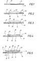
- FIG. 1 shows a first method step, wherein a first contact layer 12 and a first electrode layer 14 are applied to a base support 10, wherein the first contact layer 12 and the first electrode layer 14 are separated from each other by a separation surface 16, i. are spaced.
- the base carrier 10 may be a flexible carrier, for example a film of a plastic material.
- the carrier can - as has already been mentioned - also have other mechanical and optical properties.
- an electrically insulating first confining layer 18 is applied to the base carrier 10 at the separating surface 16 and an electrically insulating second confining layer 20 is applied to the first electrode layer 14 in a subsequent method step, as illustrated in FIG Electrode layer 14 between the first and the second boundary layer 18 and 20, a functional area 22 and a second contact surface 24 facing away from the first contact layer 12 remain free.
- FIG. 3 illustrates the method step following the method step according to FIG. 2, in which a functional layer 26 of a PDLCD mixture provided in a porous support matrix is applied and dried on the functional region 22.
- a protective layer 28 is applied to the functional layer 26 from the cured PDLCD mixture provided in the porous support matrix between the first delimiting layer 18 and the second delimiting layer 20.
- This protective layer 28 may be, for example, a conductive PEDOT / PSS layer or a non-conductive, thin, acting film-forming layer.
- This fourth method step is illustrated in FIG.
- a second electrode layer 30 is applied to the protective layer 28 and projects beyond the protective layer 28 with a projection 32 on the first contact layer 12.
- the supernatant 32 is contacted by means of a conductive connection layer 34 with the first contact layer 12.
- the second electrode layer 30 may be provided on a cover carrier 36 and laminated onto the protective layer 28.
- the cover carrier 36 may preferably be a flexible cover carrier, as in the case of the base carrier 10, so that it is possible to carry out the method according to FIGS. 1 to 5 in a roll-to-roll process. After carrying out the said process, the base support 10 and / or the cover carrier 36 can be detached. If the first electrode layer 14 is opaque, the second electrode layer 30 must be translucent - and vice versa. Likewise, it is, for example, possible that both electrode layers 14 and 30 are translucent.
Landscapes
- Physics & Mathematics (AREA)
- Nonlinear Science (AREA)
- Chemical & Material Sciences (AREA)
- Crystallography & Structural Chemistry (AREA)
- General Physics & Mathematics (AREA)
- Optics & Photonics (AREA)
- Dispersion Chemistry (AREA)
- Mathematical Physics (AREA)
- Liquid Crystal (AREA)
- Devices For Indicating Variable Information By Combining Individual Elements (AREA)
- Electroluminescent Light Sources (AREA)
Abstract
Description
- Die Erfindung betrifft ein Verfahren zur Herstellung von LCDs (Liquid Crystal Display). Bei diesen LCDs kann es sich insbesondere um PDLCDs (Polymer Dispersed-LCDs) handeln, die bspw. in einem Rolle-zu-Rolle-Prozess hergestellt werden sollen.
- Die Herstellung von PDLCDs in einem Rolle-zu-Rolle-Prozess wird bislang dadurch behindert, dass die Funktionsschicht der jeweiligen PDLCD, die aus einer mit LC-Material befüllten porösen Polymer- d.h. Stützmatrix besteht, oberflächlich nicht geschlossen ist. Nach dem Aushärten der Matrix liegen die LCs in einem nicht vernetzten, flüssigen Zustand vor. Aufgrund der an der Oberfläche der Matrix befindlichen flüssigen LCs ist es bislang nicht möglich, einen üblicherweise mehrstufigen Rolle-zu-Rolle-Prozess durchzuführen, weil die Funktionsschicht mit anderen mit ihr in Kontakt gebrachten Oberflächen verkleben würde. Daraus würde eine Beschädigung der Funktionsschicht resultieren.
- Deshalb liegt der Erfindung die Aufgabe zugrunde, ein Verfahren der eingangs genannten Art zu schaffen, wobei ein solches Verkleben der Funktionsschicht mit anderen mit ihr in Kontakt gebrachten Oberflächen verhindert und folglich eine Beschädigung der Funktionsschicht vermieden wird.
- Diese Aufgabe wird erfindungsgemäß durch die Merkmale des Anspruches 1, d.h. durch die folgenden Verfahrensschritte gelöst:
- Aufbringen einer ersten Kontaktschicht und einer davon durch eine Trennfläche beabstandeten ersten Elektrodenschicht auf einem Grundträger,
- Aufbringen einer elektrisch isolierenden ersten Begrenzungsschicht auf dem Grundträger an der Trennfläche und einer elektrisch isolierenden zweiten Begrenzungsschicht auf der ersten Elektrodenschicht, wobei an der ersten Elektrodenschicht ein Funktionsbereich und eine von der ersten Kontaktschicht abgewandte zweite Kontaktfläche frei bleibt,
- Aufbringen einer Funktionsschicht einer in einer porösen Stützmatrix vorgesehenen PDLCD-Mischung im Funktionsbereich zwischen der ersten und der zweiten Begrenzungsschicht und Aushärten der PDLCD-Mischung,
- Aufbringen einer Schutzschicht auf die ausgehärtete PDLCD-Mischung zwischen der ersten und der zweiten Begrenzungsschicht, und
- Aufbringen einer zweiten Elektrodenschicht auf die Schutzschicht, wobei die zweite Elektrodenschicht an der ersten Kontaktschicht über die Schutzschicht mit einem Überstand übersteht und der Überstand mittels einer leitfähigen Verbindungslage mit der ersten Kontaktschicht kontaktiert wird.
- Mit Hilfe der Schutzschicht wird die Funktionsschicht nach außen hin abgedichtet, so dass das Aufbringen der zweiten Elektrodenschicht auf die Schutzschicht problemlos möglich ist.
- Bei dem erfindungsgemäßen Verfahren kann als Schutzschicht eine PEDOT/PSS-Schicht oder eine nicht leitfähige, dünne, filmbildende Schicht verwendet werden. Unabhängig davon, ob eine leitfähige oder eine nicht leitfähige Schutzschicht verwendet wird, kommt es zu einem Verschließen der mit LC gefüllten Poren der Funktionsschicht aus einer in einer porösen Stützmatrix vorgesehen PDLCD-Mischung. Die solchermaßen oberflächlich trockene Funktionsschicht erlaubt die Weiterverarbeitung mit herkömmlichen Prozessen, wie Druckprozessen, Laminierprozessen o. dgl.
- Bei dem erfindungsgemäßen Verfahren kann als Grundträger ein flexibler Träger verwendet werden. Desgleichen ist es möglich, dass der Träger nicht flexibel, d.h. formstabil ist. Der Träger kann vollflächig oder teilflächig transparent, semitransparent oder nicht transparent sein. Der Träger kann selbst eine der Elektroden bilden. Bei einer solchen Ausbildung der zuletzt genannten Art ist es erforderlich, vor dem Applizieren der zweiten Elektrode eine elektrische Isolierschicht vorzusehen.
- Der Träger kann als Schrumpffolie ausgebildet sein, er kann bedruckt oder unbedruckt sein, er kann - im Falle einer Prägefolie - nur einen Zwischenträger bilden, er kann repliziert oder nicht repliziert sein, er kann selektiv Licht absorbierend usw. sein.
- Die erfindungsgemäße LCD kann eine viereckige bzw. rechteckige Grundfläche besitzen oder in jeder beliebigen anderen Grundflächenform ausgebildet sein.
- Die zweite Elektrodenschicht kann an einem Deckträger vorgesehen und auf die Schutzschicht auflaminiert sein. Bei dem Deckträger kann es sich - wie bei dem Grundträger - um einen flexiblen Deckträger handeln, so dass es einfach und hochproduktiv möglich ist, das erfindungsgemäße Verfahren in einem Rolle-zu-Rolle-Prozess durchzuführen. Auf diese Weise ist es möglich, PDLCDs kontinuierlich herzustellen.
- Weitere Einzelheiten, Merkmale und Vorteile ergeben sich aus der nachfolgenden Beschreibung von in den Zeichnungen dargestellten aufeinanderfolgenden Verfahrensschritten eines Ausführungsbeispieles des erfindungsgemäßen Verfahrens zur Herstellung von PDLCDs.
- Figur 1 zeigt einen ersten Verfahrensschritt, wobei auf einen Grundträger 10 eine erste Kontaktschicht 12 und eine erste Elektrodenschicht 14 aufgebracht werden, wobei die erste Kontaktschicht 12 und die erste Elektrodenschicht 14 voneinander durch eine Trennfläche 16 getrennt d.h. beabstandet sind.
- Bei dem Grundträger 10 kann es sich um einen flexiblen Träger, bspw. um eine Folie aus einem Kunststoffmaterial, handeln. Der Träger kann - wie bereits erwähnt worden ist - auch andere mechanische sowie optische Eigenschaften besitzen.
- Nach dem ersten Verfahrensschritt werden in einem anschließenden Verfahrensschritt, wie er in Figur 2 verdeutlicht ist, auf den Grundträger 10 an der Trennfläche 16 eine elektrisch isolierende erste Begrenzungsschicht 18 und auf der ersten Elektrodenschicht 14 eine elektrisch isolierende zweite Begrenzungsschicht 20 aufgebracht, wobei an der ersten Elektrodenschicht 14 zwischen der ersten und der zweiten Begrenzungsschicht 18 und 20 ein Funktionsbereich 22 und eine von der ersten Kontaktschicht 12 abgewandte zweite Kontaktfläche 24 frei bleiben.
- Figur 3 verdeutlicht den an den Verfahrensschritt gemäß Figur 2 anschließenden Verfahrensschritt, bei welchem auf dem Funktionsbereich 22 eine Funktionsschicht 26 aus einer in einer porösen Stützmatrix vorgesehenen PDLCD-Mischung aufgebracht und getrocknet wird.
- In einem an den Verfahrensschritt gemäß Figur 3 anschließenden Verfahrensschritt wird auf die Funktionsschicht 26 aus der in der porösen Stützmatrix vorgesehenen ausgehärteten PDLCD-Mischung zwischen der ersten Begrenzungsschicht 18 und der zweiten Begrenzungsschicht 20 eine Schutzschicht 28 aufgebracht. Bei dieser Schutzschicht 28 kann es sich bspw. um eine leitfähige PEDOT/PSS-Schicht oder um eine nicht leitfähige, dünne, filmbildende Schicht handeln. Dieser vierte Verfahrensschritt ist in Figur 4 verdeutlicht.
- In einem in Figur 5 dargestellten anschließenden Verfahrensschritt wird auf die Schutzschicht 28 eine zweite Elektrodenschicht 30 aufgebracht, die an der ersten Kontaktschicht 12 über die Schutzschicht 28 mit einem Überstand 32 übersteht. Der Überstand 32 wird mittels einer leitfähigen Verbindungslage 34 mit der ersten Kontaktschicht 12 kontaktiert.
- Die zweite Elektrodenschicht 30 kann an einem Deckträger 36 vorgesehen sein und auf die Schutzschicht 28 auflaminiert werden. Bei dem Deckträger 36 kann es sich wie bei dem Grundträger 10 vorzugsweise um einen flexiblen Deckträger werden, so dass es möglich ist, das Verfahren gemäß den Figuren 1 bis 5 in einem Rolle-zu-Rolle-Prozess durchzuführen. Nach Durchführung des besagten Prozesses können der Grundträger 10 und/oder der Deckträger 36 abgelöst werden. Ist die erste Elektrodenschicht 14 lichtundurchlässig, so muss die zweite Elektrodenschicht 30 lichtdurchlässig sein - und vice versa. Desgleichen ist es bspw. möglich, dass beide Elektrodenschichten 14 und 30 lichtdurchlässig sind.
- Gleiche Einzelheiten sind in den Figuren 1 bis 5 jeweils mit denselben Bezugsziffern bezeichnet, so dass es sich erübrigt, in Verbindung mit allen Figuren alle Einzelheiten jeweils detailliert zu beschreiben.
Claims (10)
- Verfahren zur Herstellung von LCDS, insbesondere PDLCDs gekennzeichnet durch die Verfahrensschritte:Aufbringen einer ersten Kontaktschicht (12) und einer davon durch eine Trennfläche (16) beabstandeten ersten Elektrodenschicht (14) auf einen Grundträger (10),Aufbringen einer elektrisch isolierenden ersten Begrenzungsschicht (18) auf den Grundträger (10) an der Trennfläche (16) und einer elektrisch isolierenden zweiten Begrenzungsschicht (20) auf der ersten Elektrodenschicht (14), wobei an der ersten Elektrodenschicht (14) ein Funktionsbereich (22) und eine von der ersten Kontaktschicht (2) abgewandte zweite Kontaktfläche (24) frei bleibt,Aufbringen einer Funktionsschicht (26) aus einer in einer porösen Stützmatrix vorgesehenen PDLCD-Mischung im Funktionsbereich (22) zwischen der ersten und zweiten Begrenzungsschicht (28) und Aushärten der Funktionsschicht (26),Aufbringen einer Schutzschicht (28) auf die Funktionsschicht (26) zwischen der ersten und der zweiten Begrenzungsschicht (18 und 20), undAufbringen einer zweiten Elektrodenschicht (30) auf die Schutzschicht (28), wobei die zweite Elektrodenschicht (30) an der ersten Kontaktschicht (12) über die Schutzschicht (28) mit einem Überstand (32) übersteht und der Überstand (32) mittels einer leitfähigen Verbindungslage (34) mit der ersten Kontaktschicht (12) kontaktiert wird.
- Verfahren nach Anspruch 1,
dadurch gekennzeichnet,
dass als Grundträger (10) ein flexibler Träger verwendet wird. - Verfahren nach Anspruch 1,
dadurch gekennzeichnet,
dass für die erste Elektrodenschicht (14) ein PEDOT/PSS- oder ein ITO-Elektrodenmaterial verwendet wird. - Verfahren nach Anspruch 1,
dadurch gekennzeichnet,
dass als Funktionsschicht (26) eine klebrige PDLCD-Mischung in einer vernetzten porösen Stützmatrix verwendet wird. - Verfahren nach Anspruch 4,
dadurch gekennzeichnet,
dass die PDLCD-Mischung in unterschiedlichen Konzentrationsverhältnissen vorgesehen ist. - Verfahren nach Anspruch 1,
dadurch gekennzeichnet,
dass als Schutzschicht (28) eine PEDOT/PSS-Schicht verwendet wird. - Verfahren nach Anspruch 1,
dadurch gekennzeichnet,
dass als Schutzschicht (28) eine nicht leitfähige, dünne, filmbildende Schicht verwendet wird. - Verfahren nach Anspruch 1,
dadurch gekennzeichnet,
dass die zweite Elektrodenschicht (30) an einem Deckträger (36) vorgesehen
ist und auf die Schutzschicht (28) auflaminiert wird. - Verfahren nach Anspruch 8,
dadurch gekennzeichnet,
dass als Deckträger (36) ein flexibler Deckträger verwendet wird. - Verfahren nach einem der Ansprüche 1 bis 9,
dadurch gekennzeichnet,
dass ein Rolle-zu-Rolle-Prozess durchgeführt wird.
Applications Claiming Priority (1)
| Application Number | Priority Date | Filing Date | Title |
|---|---|---|---|
| DE102006052606A DE102006052606B4 (de) | 2006-11-08 | 2006-11-08 | Verfahren zur Herstellung von PDLCDs |
Publications (2)
| Publication Number | Publication Date |
|---|---|
| EP1921492A1 true EP1921492A1 (de) | 2008-05-14 |
| EP1921492B1 EP1921492B1 (de) | 2009-01-07 |
Family
ID=38863057
Family Applications (1)
| Application Number | Title | Priority Date | Filing Date |
|---|---|---|---|
| EP07021534A Active EP1921492B1 (de) | 2006-11-08 | 2007-11-06 | Verfahren zur Herstellung von Flüssigkristallanzeigen |
Country Status (6)
| Country | Link |
|---|---|
| US (1) | US7583333B2 (de) |
| EP (1) | EP1921492B1 (de) |
| JP (1) | JP5193566B2 (de) |
| KR (1) | KR101412410B1 (de) |
| AT (1) | ATE420388T1 (de) |
| DE (2) | DE102006052606B4 (de) |
Families Citing this family (4)
| Publication number | Priority date | Publication date | Assignee | Title |
|---|---|---|---|---|
| US9810963B2 (en) | 2013-03-07 | 2017-11-07 | Switch Materials, Inc. | Seal and seal system for a layered device |
| JP2017504057A (ja) | 2013-12-19 | 2017-02-02 | スイッチ マテリアルズ インコーポレイテッドSwitch Materials Inc. | スイッチング可能な物体および製造方法 |
| CN110794608B (zh) * | 2019-11-06 | 2022-03-11 | 福耀玻璃工业集团股份有限公司 | 一种pdlc调光膜及其封边工艺 |
| CN111552130A (zh) * | 2020-06-17 | 2020-08-18 | 苏州绘格光电科技有限公司 | 调光膜及其制备方法 |
Citations (4)
| Publication number | Priority date | Publication date | Assignee | Title |
|---|---|---|---|---|
| WO2001067170A1 (en) * | 2000-03-03 | 2001-09-13 | Sipix Imaging, Inc. | Electrophoretic display |
| WO2003104884A2 (en) * | 2002-06-10 | 2003-12-18 | E Ink Corporation | Components and methods for electro-optic displays |
| EP1447706A2 (de) | 2003-02-13 | 2004-08-18 | Eastman Kodak Company | Anzeigevorrichtung mit polymerdispergiertem cholesterischem Flüssigkristall und deren Herstellungsverfahren |
| EP1712949A1 (de) | 2003-12-19 | 2006-10-18 | Bridgestone Corporation | Verfahren zur herstellung eines informations-display |
Family Cites Families (19)
| Publication number | Priority date | Publication date | Assignee | Title |
|---|---|---|---|---|
| JPH03229218A (ja) * | 1990-02-02 | 1991-10-11 | Asahi Glass Co Ltd | 液晶調光積層体及びその製造方法 |
| US5354498A (en) * | 1990-03-16 | 1994-10-11 | Fuji Xerox Co., Ltd. | Phase separation liquid crystal polymer |
| JPH0437820A (ja) * | 1990-06-04 | 1992-02-07 | Seiko Epson Corp | 液晶表示素子の製造方法 |
| JPH0437821A (ja) * | 1990-06-04 | 1992-02-07 | Ajinomoto Co Inc | 液晶光学素子及びその製造方法 |
| JP3197055B2 (ja) * | 1992-04-20 | 2001-08-13 | 大日本印刷株式会社 | カード型液晶記録媒体作製方法及び該方法により作製された液晶記録媒体。 |
| US5673127A (en) * | 1993-12-01 | 1997-09-30 | Matsushita Electric Industrial Co., Ltd. | Display panel and display device using a display panel |
| JP3455759B2 (ja) * | 1993-12-24 | 2003-10-14 | カシオ計算機株式会社 | 高分子分散型液晶表示素子の製造装置及び製造方法 |
| JPH07270763A (ja) * | 1994-04-01 | 1995-10-20 | Pilot Corp:The | 液晶表示素子 |
| JPH095715A (ja) * | 1995-06-14 | 1997-01-10 | Fuji Xerox Co Ltd | 高分子液晶デバイスの作製方法 |
| JPH1152395A (ja) * | 1997-08-06 | 1999-02-26 | Hitachi Ltd | 液晶表示装置とその製造方法 |
| JP2001125086A (ja) * | 1999-10-29 | 2001-05-11 | Citizen Watch Co Ltd | ポリマーネットワーク型液晶表示装置の製造方法 |
| JP2001174792A (ja) * | 2000-12-18 | 2001-06-29 | Seiko Epson Corp | 表示装置及び表示装置の製造方法 |
| EP1377873B1 (de) | 2001-02-12 | 2013-11-06 | Samsung Display Co., Ltd. | Flüssigkristallanzeigen, aufgebaut mit polymerisierungseinleitungs- und verbesserungselementen, die zwischen substraten positioniert sind |
| EP1360548B1 (de) | 2001-02-12 | 2006-11-29 | Samsung Electronics Co., Ltd. | Elektrooptische displays mit mehrschichtstruktur, die durch variierende geschwindigkeiten der polymerisierung erreicht wird |
| JP2004070069A (ja) * | 2002-08-07 | 2004-03-04 | Ricoh Co Ltd | 積層基板の製造方法・積層型液晶表示素子の製造方法 |
| TW594339B (en) * | 2003-03-12 | 2004-06-21 | Ind Tech Res Inst | Liquid crystal display manufacture method |
| KR100653471B1 (ko) * | 2003-03-31 | 2006-12-04 | 비오이 하이디스 테크놀로지 주식회사 | 컬러 고분자 분산 액정표시장치 및 그 제조방법 |
| US7259106B2 (en) * | 2004-09-10 | 2007-08-21 | Versatilis Llc | Method of making a microelectronic and/or optoelectronic circuitry sheet |
| JP2006133645A (ja) * | 2004-11-09 | 2006-05-25 | Konica Minolta Holdings Inc | 液晶表示素子の製造方法及び液晶表示素子 |
-
2006
- 2006-11-08 DE DE102006052606A patent/DE102006052606B4/de not_active Expired - Fee Related
-
2007
- 2007-11-01 US US11/981,904 patent/US7583333B2/en not_active Expired - Fee Related
- 2007-11-06 EP EP07021534A patent/EP1921492B1/de active Active
- 2007-11-06 DE DE502007000367T patent/DE502007000367D1/de active Active
- 2007-11-06 AT AT07021534T patent/ATE420388T1/de active
- 2007-11-08 JP JP2007290560A patent/JP5193566B2/ja not_active Expired - Fee Related
- 2007-11-08 KR KR1020070113884A patent/KR101412410B1/ko active IP Right Grant
Patent Citations (4)
| Publication number | Priority date | Publication date | Assignee | Title |
|---|---|---|---|---|
| WO2001067170A1 (en) * | 2000-03-03 | 2001-09-13 | Sipix Imaging, Inc. | Electrophoretic display |
| WO2003104884A2 (en) * | 2002-06-10 | 2003-12-18 | E Ink Corporation | Components and methods for electro-optic displays |
| EP1447706A2 (de) | 2003-02-13 | 2004-08-18 | Eastman Kodak Company | Anzeigevorrichtung mit polymerdispergiertem cholesterischem Flüssigkristall und deren Herstellungsverfahren |
| EP1712949A1 (de) | 2003-12-19 | 2006-10-18 | Bridgestone Corporation | Verfahren zur herstellung eines informations-display |
Also Published As
| Publication number | Publication date |
|---|---|
| US7583333B2 (en) | 2009-09-01 |
| KR101412410B1 (ko) | 2014-07-02 |
| US20080170182A1 (en) | 2008-07-17 |
| JP5193566B2 (ja) | 2013-05-08 |
| ATE420388T1 (de) | 2009-01-15 |
| DE502007000367D1 (de) | 2009-02-26 |
| EP1921492B1 (de) | 2009-01-07 |
| JP2008122962A (ja) | 2008-05-29 |
| DE102006052606A1 (de) | 2008-05-15 |
| KR20080042026A (ko) | 2008-05-14 |
| DE102006052606B4 (de) | 2008-09-18 |
Similar Documents
| Publication | Publication Date | Title |
|---|---|---|
| EP0129697B1 (de) | Verfahren zur Herstellung von gedruckten Schaltungen | |
| DE3105981C2 (de) | Flüssigkristallanzeigeeinrichtung | |
| DE102006023138B4 (de) | LCD und Verfahren zu dessen Herstellung | |
| DE1258940B (de) | Verfahren zur Herstellung gedruckter Schaltungen | |
| DE19603451A1 (de) | Organische elektrolumineszente Anzeigevorrichutng und Verfahren zur Herstellung derselbigen | |
| EP1921492B1 (de) | Verfahren zur Herstellung von Flüssigkristallanzeigen | |
| DE1465746A1 (de) | Verfahren zur Herstellung gedruckter Schaltungen | |
| DE102014108433A1 (de) | Verfahren zur Herstellung eines Touch-Substrates | |
| DE102008030441B3 (de) | Lichtventilanordnung mit schaltbarer Transparenz und Verfahren zu deren Herstellung | |
| DE3527683A1 (de) | Tastenschalteranordnung | |
| DE10252308B3 (de) | Verfahren zur Herstellung einer Halberzeugnisleiterplatte | |
| WO2016116499A1 (de) | Folienverbund mit elektrischer funktionalität und kontaktierung zum kontaktieren eines elektrischen leiters | |
| EP1550358A2 (de) | Leiterplatte mit mindestens einem starren und mindestens einem flexiblen bereich sowie verfahren zur herstellung von starr-flexiblen leiterplatten | |
| DE102007051930A1 (de) | Verfahren zur Herstellung einer Leiterbahnstruktur | |
| DE1302727B (de) | ||
| DE3031751A1 (de) | Verfahren zur herstellung elektrotechnischer bauteile und nach diesem verfahren hergestellter schiebe- oder drehwiderstand | |
| DE3403799C2 (de) | ||
| DE102008053351B3 (de) | Bedienfeld für ein Tastaturmodul, Tastaturmodul und Verfahren zu deren Herstellung | |
| DE2615323A1 (de) | Elektrooptische zelle und verfahren zu ihrer herstellung | |
| AT514564A4 (de) | Verfahren zum Ankontaktieren und Umverdrahten | |
| EP1808058A1 (de) | Verfahren zur herstellung einer dreidimensionalen schaltung | |
| DE3411477A1 (de) | Eingangselement | |
| EP2018793B1 (de) | Verfahren zum herstellen einer elektrolumineszenzanordnung sowie nach einem solchen verfahren hergestellte elektrolumineszenzanordnung | |
| DE102005002149A1 (de) | Tastatur und Verfahren zur Herstellung einer Tastatur | |
| DE102018132598A1 (de) | Elektroaktives Polymer-Wandlergerät |
Legal Events
| Date | Code | Title | Description |
|---|---|---|---|
| PUAI | Public reference made under article 153(3) epc to a published international application that has entered the european phase |
Free format text: ORIGINAL CODE: 0009012 |
|
| AK | Designated contracting states |
Kind code of ref document: A1 Designated state(s): AT BE BG CH CY CZ DE DK EE ES FI FR GB GR HU IE IS IT LI LT LU LV MC MT NL PL PT RO SE SI SK TR |
|
| AX | Request for extension of the european patent |
Extension state: AL BA HR MK RS |
|
| 17P | Request for examination filed |
Effective date: 20080409 |
|
| GRAP | Despatch of communication of intention to grant a patent |
Free format text: ORIGINAL CODE: EPIDOSNIGR1 |
|
| GRAS | Grant fee paid |
Free format text: ORIGINAL CODE: EPIDOSNIGR3 |
|
| GRAA | (expected) grant |
Free format text: ORIGINAL CODE: 0009210 |
|
| AK | Designated contracting states |
Kind code of ref document: B1 Designated state(s): AT BE BG CH CY CZ DE DK EE ES FI FR GB GR HU IE IS IT LI LT LU LV MC MT NL PL PT RO SE SI SK TR |
|
| REG | Reference to a national code |
Ref country code: GB Ref legal event code: FG4D Free format text: NOT ENGLISH |
|
| REG | Reference to a national code |
Ref country code: CH Ref legal event code: EP |
|
| AKX | Designation fees paid |
Designated state(s): AT BE BG CH CY CZ DE DK EE ES FI FR GB GR HU IE IS IT LI LT LU LV MC MT NL PL PT RO SE SI SK TR |
|
| REG | Reference to a national code |
Ref country code: CH Ref legal event code: NV Representative=s name: FIAMMENGHI-FIAMMENGHI |
|
| REG | Reference to a national code |
Ref country code: IE Ref legal event code: FG4D Free format text: LANGUAGE OF EP DOCUMENT: GERMAN |
|
| REF | Corresponds to: |
Ref document number: 502007000367 Country of ref document: DE Date of ref document: 20090226 Kind code of ref document: P |
|
| PG25 | Lapsed in a contracting state [announced via postgrant information from national office to epo] |
Ref country code: NL Free format text: LAPSE BECAUSE OF FAILURE TO SUBMIT A TRANSLATION OF THE DESCRIPTION OR TO PAY THE FEE WITHIN THE PRESCRIBED TIME-LIMIT Effective date: 20090107 Ref country code: SI Free format text: LAPSE BECAUSE OF FAILURE TO SUBMIT A TRANSLATION OF THE DESCRIPTION OR TO PAY THE FEE WITHIN THE PRESCRIBED TIME-LIMIT Effective date: 20090107 |
|
| NLV1 | Nl: lapsed or annulled due to failure to fulfill the requirements of art. 29p and 29m of the patents act | ||
| PG25 | Lapsed in a contracting state [announced via postgrant information from national office to epo] |
Ref country code: ES Free format text: LAPSE BECAUSE OF FAILURE TO SUBMIT A TRANSLATION OF THE DESCRIPTION OR TO PAY THE FEE WITHIN THE PRESCRIBED TIME-LIMIT Effective date: 20090418 Ref country code: FI Free format text: LAPSE BECAUSE OF FAILURE TO SUBMIT A TRANSLATION OF THE DESCRIPTION OR TO PAY THE FEE WITHIN THE PRESCRIBED TIME-LIMIT Effective date: 20090107 Ref country code: LT Free format text: LAPSE BECAUSE OF FAILURE TO SUBMIT A TRANSLATION OF THE DESCRIPTION OR TO PAY THE FEE WITHIN THE PRESCRIBED TIME-LIMIT Effective date: 20090107 |
|
| REG | Reference to a national code |
Ref country code: IE Ref legal event code: FD4D |
|
| PG25 | Lapsed in a contracting state [announced via postgrant information from national office to epo] |
Ref country code: PT Free format text: LAPSE BECAUSE OF FAILURE TO SUBMIT A TRANSLATION OF THE DESCRIPTION OR TO PAY THE FEE WITHIN THE PRESCRIBED TIME-LIMIT Effective date: 20090608 Ref country code: SE Free format text: LAPSE BECAUSE OF FAILURE TO SUBMIT A TRANSLATION OF THE DESCRIPTION OR TO PAY THE FEE WITHIN THE PRESCRIBED TIME-LIMIT Effective date: 20090407 Ref country code: PL Free format text: LAPSE BECAUSE OF FAILURE TO SUBMIT A TRANSLATION OF THE DESCRIPTION OR TO PAY THE FEE WITHIN THE PRESCRIBED TIME-LIMIT Effective date: 20090107 Ref country code: LV Free format text: LAPSE BECAUSE OF FAILURE TO SUBMIT A TRANSLATION OF THE DESCRIPTION OR TO PAY THE FEE WITHIN THE PRESCRIBED TIME-LIMIT Effective date: 20090107 Ref country code: IS Free format text: LAPSE BECAUSE OF FAILURE TO SUBMIT A TRANSLATION OF THE DESCRIPTION OR TO PAY THE FEE WITHIN THE PRESCRIBED TIME-LIMIT Effective date: 20090507 |
|
| PG25 | Lapsed in a contracting state [announced via postgrant information from national office to epo] |
Ref country code: IE Free format text: LAPSE BECAUSE OF FAILURE TO SUBMIT A TRANSLATION OF THE DESCRIPTION OR TO PAY THE FEE WITHIN THE PRESCRIBED TIME-LIMIT Effective date: 20090107 Ref country code: EE Free format text: LAPSE BECAUSE OF FAILURE TO SUBMIT A TRANSLATION OF THE DESCRIPTION OR TO PAY THE FEE WITHIN THE PRESCRIBED TIME-LIMIT Effective date: 20090107 Ref country code: DK Free format text: LAPSE BECAUSE OF FAILURE TO SUBMIT A TRANSLATION OF THE DESCRIPTION OR TO PAY THE FEE WITHIN THE PRESCRIBED TIME-LIMIT Effective date: 20090107 Ref country code: CZ Free format text: LAPSE BECAUSE OF FAILURE TO SUBMIT A TRANSLATION OF THE DESCRIPTION OR TO PAY THE FEE WITHIN THE PRESCRIBED TIME-LIMIT Effective date: 20090107 |
|
| PLBE | No opposition filed within time limit |
Free format text: ORIGINAL CODE: 0009261 |
|
| STAA | Information on the status of an ep patent application or granted ep patent |
Free format text: STATUS: NO OPPOSITION FILED WITHIN TIME LIMIT |
|
| PG25 | Lapsed in a contracting state [announced via postgrant information from national office to epo] |
Ref country code: SK Free format text: LAPSE BECAUSE OF FAILURE TO SUBMIT A TRANSLATION OF THE DESCRIPTION OR TO PAY THE FEE WITHIN THE PRESCRIBED TIME-LIMIT Effective date: 20090107 Ref country code: RO Free format text: LAPSE BECAUSE OF FAILURE TO SUBMIT A TRANSLATION OF THE DESCRIPTION OR TO PAY THE FEE WITHIN THE PRESCRIBED TIME-LIMIT Effective date: 20090107 |
|
| 26N | No opposition filed |
Effective date: 20091008 |
|
| PG25 | Lapsed in a contracting state [announced via postgrant information from national office to epo] |
Ref country code: BG Free format text: LAPSE BECAUSE OF FAILURE TO SUBMIT A TRANSLATION OF THE DESCRIPTION OR TO PAY THE FEE WITHIN THE PRESCRIBED TIME-LIMIT Effective date: 20090407 |
|
| BERE | Be: lapsed |
Owner name: LEONHARD KURZ STIFTUNG & CO. K.G. Effective date: 20091130 |
|
| PG25 | Lapsed in a contracting state [announced via postgrant information from national office to epo] |
Ref country code: MC Free format text: LAPSE BECAUSE OF NON-PAYMENT OF DUE FEES Effective date: 20091130 |
|
| PG25 | Lapsed in a contracting state [announced via postgrant information from national office to epo] |
Ref country code: BE Free format text: LAPSE BECAUSE OF NON-PAYMENT OF DUE FEES Effective date: 20091130 Ref country code: GR Free format text: LAPSE BECAUSE OF FAILURE TO SUBMIT A TRANSLATION OF THE DESCRIPTION OR TO PAY THE FEE WITHIN THE PRESCRIBED TIME-LIMIT Effective date: 20090408 |
|
| PG25 | Lapsed in a contracting state [announced via postgrant information from national office to epo] |
Ref country code: IT Free format text: LAPSE BECAUSE OF FAILURE TO SUBMIT A TRANSLATION OF THE DESCRIPTION OR TO PAY THE FEE WITHIN THE PRESCRIBED TIME-LIMIT Effective date: 20090107 |
|
| PG25 | Lapsed in a contracting state [announced via postgrant information from national office to epo] |
Ref country code: LU Free format text: LAPSE BECAUSE OF NON-PAYMENT OF DUE FEES Effective date: 20091106 |
|
| PG25 | Lapsed in a contracting state [announced via postgrant information from national office to epo] |
Ref country code: HU Free format text: LAPSE BECAUSE OF FAILURE TO SUBMIT A TRANSLATION OF THE DESCRIPTION OR TO PAY THE FEE WITHIN THE PRESCRIBED TIME-LIMIT Effective date: 20090708 |
|
| PG25 | Lapsed in a contracting state [announced via postgrant information from national office to epo] |
Ref country code: TR Free format text: LAPSE BECAUSE OF FAILURE TO SUBMIT A TRANSLATION OF THE DESCRIPTION OR TO PAY THE FEE WITHIN THE PRESCRIBED TIME-LIMIT Effective date: 20090107 |
|
| PG25 | Lapsed in a contracting state [announced via postgrant information from national office to epo] |
Ref country code: CY Free format text: LAPSE BECAUSE OF FAILURE TO SUBMIT A TRANSLATION OF THE DESCRIPTION OR TO PAY THE FEE WITHIN THE PRESCRIBED TIME-LIMIT Effective date: 20090107 |
|
| REG | Reference to a national code |
Ref country code: FR Ref legal event code: PLFP Year of fee payment: 9 |
|
| REG | Reference to a national code |
Ref country code: FR Ref legal event code: PLFP Year of fee payment: 10 |
|
| REG | Reference to a national code |
Ref country code: FR Ref legal event code: PLFP Year of fee payment: 11 |
|
| PGFP | Annual fee paid to national office [announced via postgrant information from national office to epo] |
Ref country code: FR Payment date: 20191121 Year of fee payment: 13 |
|
| PGFP | Annual fee paid to national office [announced via postgrant information from national office to epo] |
Ref country code: CH Payment date: 20191125 Year of fee payment: 13 Ref country code: AT Payment date: 20191119 Year of fee payment: 13 |
|
| PGFP | Annual fee paid to national office [announced via postgrant information from national office to epo] |
Ref country code: GB Payment date: 20191126 Year of fee payment: 13 |
|
| REG | Reference to a national code |
Ref country code: CH Ref legal event code: PL |
|
| REG | Reference to a national code |
Ref country code: AT Ref legal event code: MM01 Ref document number: 420388 Country of ref document: AT Kind code of ref document: T Effective date: 20201106 |
|
| GBPC | Gb: european patent ceased through non-payment of renewal fee |
Effective date: 20201106 |
|
| PG25 | Lapsed in a contracting state [announced via postgrant information from national office to epo] |
Ref country code: LI Free format text: LAPSE BECAUSE OF NON-PAYMENT OF DUE FEES Effective date: 20201130 Ref country code: CH Free format text: LAPSE BECAUSE OF NON-PAYMENT OF DUE FEES Effective date: 20201130 Ref country code: AT Free format text: LAPSE BECAUSE OF NON-PAYMENT OF DUE FEES Effective date: 20201106 |
|
| PG25 | Lapsed in a contracting state [announced via postgrant information from national office to epo] |
Ref country code: FR Free format text: LAPSE BECAUSE OF NON-PAYMENT OF DUE FEES Effective date: 20201130 |
|
| PG25 | Lapsed in a contracting state [announced via postgrant information from national office to epo] |
Ref country code: GB Free format text: LAPSE BECAUSE OF NON-PAYMENT OF DUE FEES Effective date: 20201106 |
|
| PGFP | Annual fee paid to national office [announced via postgrant information from national office to epo] |
Ref country code: DE Payment date: 20231020 Year of fee payment: 17 |