EP1909315A1 - Plaque de silicium et procede de production de celle-ci - Google Patents
Plaque de silicium et procede de production de celle-ci Download PDFInfo
- Publication number
- EP1909315A1 EP1909315A1 EP05806093A EP05806093A EP1909315A1 EP 1909315 A1 EP1909315 A1 EP 1909315A1 EP 05806093 A EP05806093 A EP 05806093A EP 05806093 A EP05806093 A EP 05806093A EP 1909315 A1 EP1909315 A1 EP 1909315A1
- Authority
- EP
- European Patent Office
- Prior art keywords
- heat treatment
- crystal
- hydrogen
- wafer
- silicon
- Prior art date
- Legal status (The legal status is an assumption and is not a legal conclusion. Google has not performed a legal analysis and makes no representation as to the accuracy of the status listed.)
- Withdrawn
Links
- XUIMIQQOPSSXEZ-UHFFFAOYSA-N Silicon Chemical compound [Si] XUIMIQQOPSSXEZ-UHFFFAOYSA-N 0.000 title claims abstract description 142
- 229910052710 silicon Inorganic materials 0.000 title claims abstract description 142
- 239000010703 silicon Substances 0.000 title claims abstract description 142
- 238000000034 method Methods 0.000 title claims abstract description 49
- 230000008569 process Effects 0.000 title description 11
- 239000013078 crystal Substances 0.000 claims abstract description 243
- 238000010438 heat treatment Methods 0.000 claims abstract description 132
- 239000012298 atmosphere Substances 0.000 claims abstract description 60
- 125000004435 hydrogen atom Chemical group [H]* 0.000 claims abstract description 52
- 239000000126 substance Substances 0.000 claims abstract description 39
- 230000001590 oxidative effect Effects 0.000 claims abstract description 5
- UFHFLCQGNIYNRP-UHFFFAOYSA-N Hydrogen Chemical compound [H][H] UFHFLCQGNIYNRP-UHFFFAOYSA-N 0.000 claims description 119
- 239000001257 hydrogen Substances 0.000 claims description 118
- 229910052739 hydrogen Inorganic materials 0.000 claims description 118
- 238000004519 manufacturing process Methods 0.000 claims description 32
- 239000002244 precipitate Substances 0.000 claims description 25
- QVGXLLKOCUKJST-UHFFFAOYSA-N atomic oxygen Chemical compound [O] QVGXLLKOCUKJST-UHFFFAOYSA-N 0.000 claims description 19
- 239000001301 oxygen Substances 0.000 claims description 19
- 229910052760 oxygen Inorganic materials 0.000 claims description 19
- 125000004429 atom Chemical group 0.000 claims description 10
- 235000012431 wafers Nutrition 0.000 abstract description 130
- 230000007547 defect Effects 0.000 description 57
- 238000000137 annealing Methods 0.000 description 32
- XKRFYHLGVUSROY-UHFFFAOYSA-N Argon Chemical compound [Ar] XKRFYHLGVUSROY-UHFFFAOYSA-N 0.000 description 30
- 238000001556 precipitation Methods 0.000 description 28
- 230000015572 biosynthetic process Effects 0.000 description 24
- 229910052786 argon Inorganic materials 0.000 description 15
- 238000009826 distribution Methods 0.000 description 14
- 230000007423 decrease Effects 0.000 description 12
- 230000000694 effects Effects 0.000 description 12
- 238000012360 testing method Methods 0.000 description 12
- 239000011261 inert gas Substances 0.000 description 11
- 239000010410 layer Substances 0.000 description 10
- 239000000155 melt Substances 0.000 description 10
- 238000010586 diagram Methods 0.000 description 9
- OKTJSMMVPCPJKN-UHFFFAOYSA-N Carbon Chemical compound [C] OKTJSMMVPCPJKN-UHFFFAOYSA-N 0.000 description 8
- 239000007789 gas Substances 0.000 description 8
- 239000012535 impurity Substances 0.000 description 8
- 230000036961 partial effect Effects 0.000 description 8
- 238000004151 rapid thermal annealing Methods 0.000 description 8
- 238000005247 gettering Methods 0.000 description 6
- 150000002431 hydrogen Chemical class 0.000 description 6
- 238000006243 chemical reaction Methods 0.000 description 5
- 230000003247 decreasing effect Effects 0.000 description 5
- 230000002401 inhibitory effect Effects 0.000 description 5
- 238000012545 processing Methods 0.000 description 5
- 230000009467 reduction Effects 0.000 description 5
- IJGRMHOSHXDMSA-UHFFFAOYSA-N Atomic nitrogen Chemical compound N#N IJGRMHOSHXDMSA-UHFFFAOYSA-N 0.000 description 4
- 229910052799 carbon Inorganic materials 0.000 description 4
- 238000002485 combustion reaction Methods 0.000 description 4
- 229910002804 graphite Inorganic materials 0.000 description 4
- 239000010439 graphite Substances 0.000 description 4
- 239000000463 material Substances 0.000 description 4
- 239000010453 quartz Substances 0.000 description 4
- 230000002829 reductive effect Effects 0.000 description 4
- 239000004065 semiconductor Substances 0.000 description 4
- VYPSYNLAJGMNEJ-UHFFFAOYSA-N silicon dioxide Inorganic materials O=[Si]=O VYPSYNLAJGMNEJ-UHFFFAOYSA-N 0.000 description 4
- 238000007711 solidification Methods 0.000 description 4
- 230000008023 solidification Effects 0.000 description 4
- 239000002344 surface layer Substances 0.000 description 4
- MYMOFIZGZYHOMD-UHFFFAOYSA-N Dioxygen Chemical compound O=O MYMOFIZGZYHOMD-UHFFFAOYSA-N 0.000 description 3
- 239000012300 argon atmosphere Substances 0.000 description 3
- 230000008859 change Effects 0.000 description 3
- 238000010276 construction Methods 0.000 description 3
- 230000001419 dependent effect Effects 0.000 description 3
- 238000005474 detonation Methods 0.000 description 3
- 229910001882 dioxygen Inorganic materials 0.000 description 3
- 239000002019 doping agent Substances 0.000 description 3
- 238000005530 etching Methods 0.000 description 3
- 238000002474 experimental method Methods 0.000 description 3
- 239000001307 helium Substances 0.000 description 3
- 229910052734 helium Inorganic materials 0.000 description 3
- SWQJXJOGLNCZEY-UHFFFAOYSA-N helium atom Chemical compound [He] SWQJXJOGLNCZEY-UHFFFAOYSA-N 0.000 description 3
- 238000002156 mixing Methods 0.000 description 3
- 238000005204 segregation Methods 0.000 description 3
- RYGMFSIKBFXOCR-UHFFFAOYSA-N Copper Chemical compound [Cu] RYGMFSIKBFXOCR-UHFFFAOYSA-N 0.000 description 2
- GRYLNZFGIOXLOG-UHFFFAOYSA-N Nitric acid Chemical compound O[N+]([O-])=O GRYLNZFGIOXLOG-UHFFFAOYSA-N 0.000 description 2
- 238000004854 X-ray topography Methods 0.000 description 2
- JUZTWRXHHZRLED-UHFFFAOYSA-N [Si].[Cu].[Cu].[Cu].[Cu].[Cu] Chemical compound [Si].[Cu].[Cu].[Cu].[Cu].[Cu] JUZTWRXHHZRLED-UHFFFAOYSA-N 0.000 description 2
- 230000000052 comparative effect Effects 0.000 description 2
- 238000011109 contamination Methods 0.000 description 2
- 229910052802 copper Inorganic materials 0.000 description 2
- 239000010949 copper Substances 0.000 description 2
- 229910021360 copper silicide Inorganic materials 0.000 description 2
- 229910000365 copper sulfate Inorganic materials 0.000 description 2
- ARUVKPQLZAKDPS-UHFFFAOYSA-L copper(II) sulfate Chemical compound [Cu+2].[O-][S+2]([O-])([O-])[O-] ARUVKPQLZAKDPS-UHFFFAOYSA-L 0.000 description 2
- 229910021419 crystalline silicon Inorganic materials 0.000 description 2
- 238000005034 decoration Methods 0.000 description 2
- 238000009792 diffusion process Methods 0.000 description 2
- 238000005516 engineering process Methods 0.000 description 2
- 238000011156 evaluation Methods 0.000 description 2
- 238000011835 investigation Methods 0.000 description 2
- 239000007788 liquid Substances 0.000 description 2
- 239000011259 mixed solution Substances 0.000 description 2
- 229910017604 nitric acid Inorganic materials 0.000 description 2
- 229910052757 nitrogen Inorganic materials 0.000 description 2
- 239000012299 nitrogen atmosphere Substances 0.000 description 2
- 230000003647 oxidation Effects 0.000 description 2
- 238000007254 oxidation reaction Methods 0.000 description 2
- 230000002093 peripheral effect Effects 0.000 description 2
- 238000005498 polishing Methods 0.000 description 2
- 230000001737 promoting effect Effects 0.000 description 2
- 239000002994 raw material Substances 0.000 description 2
- 239000000243 solution Substances 0.000 description 2
- 239000000758 substrate Substances 0.000 description 2
- HSFWRNGVRCDJHI-UHFFFAOYSA-N Acetylene Chemical compound C#C HSFWRNGVRCDJHI-UHFFFAOYSA-N 0.000 description 1
- QGZKDVFQNNGYKY-UHFFFAOYSA-N Ammonia Chemical compound N QGZKDVFQNNGYKY-UHFFFAOYSA-N 0.000 description 1
- ZOXJGFHDIHLPTG-UHFFFAOYSA-N Boron Chemical compound [B] ZOXJGFHDIHLPTG-UHFFFAOYSA-N 0.000 description 1
- OAICVXFJPJFONN-UHFFFAOYSA-N Phosphorus Chemical compound [P] OAICVXFJPJFONN-UHFFFAOYSA-N 0.000 description 1
- BLRPTPMANUNPDV-UHFFFAOYSA-N Silane Chemical compound [SiH4] BLRPTPMANUNPDV-UHFFFAOYSA-N 0.000 description 1
- 238000004220 aggregation Methods 0.000 description 1
- 230000002776 aggregation Effects 0.000 description 1
- 150000001298 alcohols Chemical class 0.000 description 1
- 229910045601 alloy Inorganic materials 0.000 description 1
- 239000000956 alloy Substances 0.000 description 1
- 229910052782 aluminium Inorganic materials 0.000 description 1
- XAGFODPZIPBFFR-UHFFFAOYSA-N aluminium Chemical compound [Al] XAGFODPZIPBFFR-UHFFFAOYSA-N 0.000 description 1
- 229910052787 antimony Inorganic materials 0.000 description 1
- WATWJIUSRGPENY-UHFFFAOYSA-N antimony atom Chemical compound [Sb] WATWJIUSRGPENY-UHFFFAOYSA-N 0.000 description 1
- 229910052785 arsenic Inorganic materials 0.000 description 1
- RQNWIZPPADIBDY-UHFFFAOYSA-N arsenic atom Chemical compound [As] RQNWIZPPADIBDY-UHFFFAOYSA-N 0.000 description 1
- 229910052796 boron Inorganic materials 0.000 description 1
- 150000001735 carboxylic acids Chemical class 0.000 description 1
- 238000004140 cleaning Methods 0.000 description 1
- 239000000356 contaminant Substances 0.000 description 1
- 230000002950 deficient Effects 0.000 description 1
- 230000006866 deterioration Effects 0.000 description 1
- 230000008034 disappearance Effects 0.000 description 1
- 239000000428 dust Substances 0.000 description 1
- 229910052732 germanium Inorganic materials 0.000 description 1
- GNPVGFCGXDBREM-UHFFFAOYSA-N germanium atom Chemical compound [Ge] GNPVGFCGXDBREM-UHFFFAOYSA-N 0.000 description 1
- 238000000227 grinding Methods 0.000 description 1
- 229910052736 halogen Inorganic materials 0.000 description 1
- 150000002367 halogens Chemical class 0.000 description 1
- 229930195733 hydrocarbon Natural products 0.000 description 1
- 150000002430 hydrocarbons Chemical class 0.000 description 1
- 150000002484 inorganic compounds Chemical class 0.000 description 1
- 229910010272 inorganic material Inorganic materials 0.000 description 1
- 229910052909 inorganic silicate Inorganic materials 0.000 description 1
- 238000003780 insertion Methods 0.000 description 1
- 230000037431 insertion Effects 0.000 description 1
- 239000012212 insulator Substances 0.000 description 1
- 229910052743 krypton Inorganic materials 0.000 description 1
- DNNSSWSSYDEUBZ-UHFFFAOYSA-N krypton atom Chemical compound [Kr] DNNSSWSSYDEUBZ-UHFFFAOYSA-N 0.000 description 1
- 239000007791 liquid phase Substances 0.000 description 1
- 238000002844 melting Methods 0.000 description 1
- 230000008018 melting Effects 0.000 description 1
- 229910052751 metal Inorganic materials 0.000 description 1
- 239000002184 metal Substances 0.000 description 1
- VNWKTOKETHGBQD-UHFFFAOYSA-N methane Chemical compound C VNWKTOKETHGBQD-UHFFFAOYSA-N 0.000 description 1
- 229910052754 neon Inorganic materials 0.000 description 1
- GKAOGPIIYCISHV-UHFFFAOYSA-N neon atom Chemical compound [Ne] GKAOGPIIYCISHV-UHFFFAOYSA-N 0.000 description 1
- 229910000069 nitrogen hydride Inorganic materials 0.000 description 1
- NJPPVKZQTLUDBO-UHFFFAOYSA-N novaluron Chemical compound C1=C(Cl)C(OC(F)(F)C(OC(F)(F)F)F)=CC=C1NC(=O)NC(=O)C1=C(F)C=CC=C1F NJPPVKZQTLUDBO-UHFFFAOYSA-N 0.000 description 1
- 150000002926 oxygen Chemical class 0.000 description 1
- 239000002245 particle Substances 0.000 description 1
- 239000012071 phase Substances 0.000 description 1
- 229910052698 phosphorus Inorganic materials 0.000 description 1
- 239000011574 phosphorus Substances 0.000 description 1
- 229910021420 polycrystalline silicon Inorganic materials 0.000 description 1
- 238000007363 ring formation reaction Methods 0.000 description 1
- 239000000523 sample Substances 0.000 description 1
- 229910000077 silane Inorganic materials 0.000 description 1
- 150000003376 silicon Chemical class 0.000 description 1
- HBMJWWWQQXIZIP-UHFFFAOYSA-N silicon carbide Chemical compound [Si+]#[C-] HBMJWWWQQXIZIP-UHFFFAOYSA-N 0.000 description 1
- 229910010271 silicon carbide Inorganic materials 0.000 description 1
- 239000007790 solid phase Substances 0.000 description 1
- 238000003860 storage Methods 0.000 description 1
- 238000005979 thermal decomposition reaction Methods 0.000 description 1
- 238000007669 thermal treatment Methods 0.000 description 1
- 229910052724 xenon Inorganic materials 0.000 description 1
- FHNFHKCVQCLJFQ-UHFFFAOYSA-N xenon atom Chemical compound [Xe] FHNFHKCVQCLJFQ-UHFFFAOYSA-N 0.000 description 1
Images


Classifications
-
- H—ELECTRICITY
- H01—ELECTRIC ELEMENTS
- H01L—SEMICONDUCTOR DEVICES NOT COVERED BY CLASS H10
- H01L21/00—Processes or apparatus adapted for the manufacture or treatment of semiconductor or solid state devices or of parts thereof
- H01L21/02—Manufacture or treatment of semiconductor devices or of parts thereof
- H01L21/04—Manufacture or treatment of semiconductor devices or of parts thereof the devices having potential barriers, e.g. a PN junction, depletion layer or carrier concentration layer
- H01L21/18—Manufacture or treatment of semiconductor devices or of parts thereof the devices having potential barriers, e.g. a PN junction, depletion layer or carrier concentration layer the devices having semiconductor bodies comprising elements of Group IV of the Periodic Table or AIIIBV compounds with or without impurities, e.g. doping materials
- H01L21/30—Treatment of semiconductor bodies using processes or apparatus not provided for in groups H01L21/20 - H01L21/26
- H01L21/322—Treatment of semiconductor bodies using processes or apparatus not provided for in groups H01L21/20 - H01L21/26 to modify their internal properties, e.g. to produce internal imperfections
- H01L21/3221—Treatment of semiconductor bodies using processes or apparatus not provided for in groups H01L21/20 - H01L21/26 to modify their internal properties, e.g. to produce internal imperfections of silicon bodies, e.g. for gettering
- H01L21/3225—Thermally inducing defects using oxygen present in the silicon body for intrinsic gettering
-
- C—CHEMISTRY; METALLURGY
- C30—CRYSTAL GROWTH
- C30B—SINGLE-CRYSTAL GROWTH; UNIDIRECTIONAL SOLIDIFICATION OF EUTECTIC MATERIAL OR UNIDIRECTIONAL DEMIXING OF EUTECTOID MATERIAL; REFINING BY ZONE-MELTING OF MATERIAL; PRODUCTION OF A HOMOGENEOUS POLYCRYSTALLINE MATERIAL WITH DEFINED STRUCTURE; SINGLE CRYSTALS OR HOMOGENEOUS POLYCRYSTALLINE MATERIAL WITH DEFINED STRUCTURE; AFTER-TREATMENT OF SINGLE CRYSTALS OR A HOMOGENEOUS POLYCRYSTALLINE MATERIAL WITH DEFINED STRUCTURE; APPARATUS THEREFOR
- C30B15/00—Single-crystal growth by pulling from a melt, e.g. Czochralski method
-
- C—CHEMISTRY; METALLURGY
- C30—CRYSTAL GROWTH
- C30B—SINGLE-CRYSTAL GROWTH; UNIDIRECTIONAL SOLIDIFICATION OF EUTECTIC MATERIAL OR UNIDIRECTIONAL DEMIXING OF EUTECTOID MATERIAL; REFINING BY ZONE-MELTING OF MATERIAL; PRODUCTION OF A HOMOGENEOUS POLYCRYSTALLINE MATERIAL WITH DEFINED STRUCTURE; SINGLE CRYSTALS OR HOMOGENEOUS POLYCRYSTALLINE MATERIAL WITH DEFINED STRUCTURE; AFTER-TREATMENT OF SINGLE CRYSTALS OR A HOMOGENEOUS POLYCRYSTALLINE MATERIAL WITH DEFINED STRUCTURE; APPARATUS THEREFOR
- C30B29/00—Single crystals or homogeneous polycrystalline material with defined structure characterised by the material or by their shape
- C30B29/02—Elements
- C30B29/06—Silicon
-
- C—CHEMISTRY; METALLURGY
- C30—CRYSTAL GROWTH
- C30B—SINGLE-CRYSTAL GROWTH; UNIDIRECTIONAL SOLIDIFICATION OF EUTECTIC MATERIAL OR UNIDIRECTIONAL DEMIXING OF EUTECTOID MATERIAL; REFINING BY ZONE-MELTING OF MATERIAL; PRODUCTION OF A HOMOGENEOUS POLYCRYSTALLINE MATERIAL WITH DEFINED STRUCTURE; SINGLE CRYSTALS OR HOMOGENEOUS POLYCRYSTALLINE MATERIAL WITH DEFINED STRUCTURE; AFTER-TREATMENT OF SINGLE CRYSTALS OR A HOMOGENEOUS POLYCRYSTALLINE MATERIAL WITH DEFINED STRUCTURE; APPARATUS THEREFOR
- C30B33/00—After-treatment of single crystals or homogeneous polycrystalline material with defined structure
- C30B33/02—Heat treatment
-
- H—ELECTRICITY
- H01—ELECTRIC ELEMENTS
- H01L—SEMICONDUCTOR DEVICES NOT COVERED BY CLASS H10
- H01L21/00—Processes or apparatus adapted for the manufacture or treatment of semiconductor or solid state devices or of parts thereof
- H01L21/02—Manufacture or treatment of semiconductor devices or of parts thereof
- H01L21/04—Manufacture or treatment of semiconductor devices or of parts thereof the devices having potential barriers, e.g. a PN junction, depletion layer or carrier concentration layer
- H01L21/18—Manufacture or treatment of semiconductor devices or of parts thereof the devices having potential barriers, e.g. a PN junction, depletion layer or carrier concentration layer the devices having semiconductor bodies comprising elements of Group IV of the Periodic Table or AIIIBV compounds with or without impurities, e.g. doping materials
- H01L21/30—Treatment of semiconductor bodies using processes or apparatus not provided for in groups H01L21/20 - H01L21/26
- H01L21/324—Thermal treatment for modifying the properties of semiconductor bodies, e.g. annealing, sintering
Definitions
- the present invention relates to a silicon wafer and a method for producing the same, particularly relates to a method for producing a silicon wafer sliced from a silicon single-crystal ingot grown by the Czochralski method.
- the invention relates to a technique suitable for use in suppressing slip dislocations and improving wafer strength.
- a single crystalline silicon wafer capable of being used as a substrate for semiconductor device and the like are produced by slicing a silicon single-crystal ingot and carrying out operations such as heat treatment and mirror polishing.
- Silicon single-crystal ingot production processes are exemplified by the Czochralski (CZ) method.
- CZ Czochralski
- the crystal In the production of a silicon single crystal by the CZ method, the crystal is grown using a quartz crucible. Therefore, oxygen is included within the crystal in a supersaturated state. Such oxygen generates thermal donors (TDs), for example, during the heat treatment steps for forming circuit in the device, and cause a problem of unstable fluctuation of resistivity of the wafer during the device production process.
- TDs thermal donors
- thermal donors In conventional low-resistance wafers doped with a dopant, thermal donors have a minimal influence on the wafer resistivity and thus do not cause a problem in actual operation.
- the resistivity of an n-type wafer drops off sharply with increasing thermal donors.
- the resistivity increases abruptly at first with increasing thermal donors. While the further increase of thermal donors changes the wafer from p-type to n-type and sharply decreases the resistivity.
- Silicon wafers are generally subjected to donor killer (DK) treatment so as to prevent fluctuation of resistivity on account of thermal donors. Silicon wafers subjected to hydrogen annealing or argon annealing are also subjected to donor killer treatment prior to the high temperature annealing treatment to inhibit fluctuation of resistivity. Thermal donors are the factors for promoting the precipitation of oxide as well as fluctuating the resistivity.
- DK donor killer
- a silicon single crystal that has been pulled by the CZ method interstitially takes up oxygen to a supersaturated state.
- the supersaturated oxygen causes microdefects known as bulk microdefects (BMDs) to occur during annealing, for example, in a wafer processing operation.
- BMDs bulk microdefects
- the device-forming region is desired to have no crystal defects. If crystal defects occur in the wafer surface on which a circuit is to be formed, such defective area causes failure of the circuits or the like.
- BMDs have a effect of gettering metal impurities or the like. Such impurities cause crystal defects.
- annealing of the silicon wafer is carried out so as to induce BMDs at the interior of the silicon wafer, thus forming an intrinsic gettering (IG) layer.
- IG intrinsic gettering
- Gettering of the impurities by the IG layer results in the formation of a denuded zone (DZ) having very few crystal defects on the surface of the silicon wafer.
- the DZ layer is essential for device formation.
- a silicon wafer on which a denuded zone (DZ) has been formed is subjected to annealing, dislocation defects (slips) occur and propagate in the DZ layer and lower the strength of the silicon wafer.
- slip dislocations sometimes propagate from the peripheral back side portion at which the wafer is supported, If a strength of a wafer is reduced, the wafer tends to generate damage or failure in subsequent process.
- Thermal donors are a factor for promoting the precipitation of oxides as well as a factor for fluctuating the resistivity. Therefore by performing low temperature heat treatment before the disappearance of thermal donors by high temperature annealing (Ar/H 2 annealing), small-size oxide precipitation nuclei can be formed in the bulk crystal to a high density. Small-size oxide precipitation nuclei have a role of inhibiting propagation of slips during high temperature thermal treatment. In a silicon wafer having a high density of precipitation nuclei, the propagation of slip dislocations is inhibited by the precipitates formed on dislocation lines in the high temperature annealing process.
- the invention provides a method for producing a silicon wafer, including:
- the invention also provides a method for producing a silicon wafer, which includes:
- the temperature in the low temperature heat treatment is not lower than 400°C but not higher than 650°C, and the temperature is increased at a rate of not lower than 0.2°C/min but not higher than 2.0°C/min.
- the low temperature heat treatment may be carried out by ramping heat treatment.
- the above-described low temperature heat treatment can be used as a step for setting the difference in oxygen concentration before and after the high temperature heat treatment, based on a value measured in accordance with ASTM-F121 1979, to not less than 1.5 ⁇ 10 17 atoms/cm 3 .
- the hydrogen concentration within the inert atmosphere in the growth of the single crystal may be set in a range of not less than 0.1% by volume but not more than 20% by volume at an atmospheric pressure of 1.3 to 13.3 kPa (10 to 100 torr) within the furnace.
- the oxide precipitate density after the high temperature heat treatment it is desirable to set the oxide precipitate density after the high temperature heat treatment to not less than 1.0 ⁇ 10 10 nuclei/cm 3 .
- the silicon wafer of the invention can be produced by either of the foregoing production methods.
- the method for producing a silicon wafer of the invention includes: growing a silicon single crystal by the Czochralski method in an inert atmosphere which includes a gaseous substance containing hydrogen atoms; slicing a wafer from the silicon single crystal; either performing a high temperature heat treatment of the wafer in a non-oxidizing atmosphere at a temperature of not lower than 1000°C but not higher than 1300°C or performing a donor killer heat treatment of the wafer to prevent fluctuation of resistivity in the wafer; and, prior to the high temperature heat treatment or donor killer heat treatment, performing a low temperature heat treatment of the wafer at a temperature lower than a temperature used in the high temperature heat treatment or the donor killer heat treatment.
- thermal donors occur to a high density within the bulk single crystal.
- TD thermal donors
- small-size oxide precipitation nuclei occur to a high density in the bulk crystal.
- the thermal donors (TD) that have been formed to a high density in the as-grown state cause to form oxide precipitates under ramping heat treatment at a low temperature.
- low temperature ramping heat treatment to a hydrogen-doped wafer which contains thermal donors at high concentration, small-size oxide precipitates can be formed to a high density in the bulk crystal.
- By performing low temperature ramping heat treatment it is possible to incorporate small-size precipitates within the bulk crystal to a high density and promote precipitation and inhibit propagation of slips.
- silicon wafers are subjected to donor killer (DK) treatment so as to prevent fluctuation of resistivity due to thermal donors.
- DK donor killer
- silicon wafers subjected to hydrogen annealing or argon annealing are subjected to donor killer treatment at 600 to 700°C for about 0.5 to 2 hours prior to high temperature annealing treatment. Therefore, in the case for performing a ramping heat treatment, it is desirable to carry it out prior to the donor killer treatment (in a state where sufficient thermal donors exist).
- preferable oxide precipitation nuclei can be formed by setting the treatment temperature in the above-described low temperature heat treatment to not lower than 400°C but not higher than 650°C and by setting the heating rate to be not lower than 0.2°C/min but not more than 2.0°C/min, and preferably not lower than 0.3°C but not more than 1.0°C/min.
- the difference in oxygen concentration before and after the high temperature heat treatment is set to be not less than 1.5 ⁇ 10 17 atoms/cm 3 (ASTM-F 121 1979), enabling the oxygen concentration to be lowered.
- ASTM-F 121 1979 As a result, it is possible to obtain a wafer having the desired oxide precipitation nuclei by precisely controlling the formation state of oxide precipitation nuclei.
- the hydrogen concentration within the inert atmosphere during the growth of a single crystal may be set in a range of not less than 0.1 % by volume but not more than 20% by volume under a atmospheric pressure of 1.3 to 13.3 kPa (10 to 100 torr) within the furnace.
- a wafer sliced from a single crystal grown in this atmosphere the desired oxide precipitation nuclei state is maintained by the above-described low temperature heat treatment, and sufficient oxide precipitation nuclei to prevent slip propagation are formed.
- the hydrogen concentration in the inert atmosphere may be set, under conditions of atmospheric pressure of 4.0 to 9.33 kPa (30 to 70 torr) within the furnace, to not less than 0.3% but not more than 10%.
- the oxide precipitate density to be not less than 1.0 ⁇ 10 10 nuclei/cm 3 after the high temperature heat treatment, slip propagation during high temperature heat treatment can be sufficiently inhibited.
- the size of the above oxide precipitates is preferably about 80 to 200 nm, and more preferably about 100 nm.
- FIGS. 1 and 2 show the density of oxide precipitation nuclei on the vertical axis and the size on the horizontal axis.
- the symbol BB represents the boundary line indicating the critical size of BMDs that remain at a temperature of not lower than 900°C.
- the density of BMDs at and above the critical BMD size at 900°C to the right of the boundary BB is on the order of 1.0 ⁇ 10 9 nuclei/cm 3 .
- the density of BMDs at or above the critical BMD size at 900°C to the right of the boundary BB is on the order of 1.0 ⁇ 10 10 nuclei/cm 3 .
- a BMD density of not less than 1.0 ⁇ 10 10 nuclei/cm 3 is ensured and slip propagation during high temperature heat treatment is inhibited by the high density of BMDs.
- the density of BMDs remaining in the wafer after high temperature annealing was found to be equivalent to the density of BMDs not smaller than the critical BMD size at 900°C.
- the boundary was set at 900°C.
- the silicon wafer of the invention can be produced by either of the methods described above.
- the OSF-developing region in a longisectional view of the single crystal has a downwardly convex U-like shape that is flat at the bottom.
- the OSF-developing region exhibits a ring-like shape inside of which can be seen a COP (also called "infrared scattering defect") developing region.
- the ring-like OSF-developing region shrinks to the center of the crystal as the pulling rate decreases. Further reduction of the pulling rate gives rise to a dislocation cluster-developing region.
- the pulling rate range for achieving a defect free state is broadened; and the defect-free region expands in the axial direction of the crystal in the defect distribution within a longitudinal section of the crystal.
- This effect can be observed by comparing the region B-C in FIG. 3 for a crystal grown without hydrogen doping with the region B'-C' in FIG. 4 for a crystal grown with hydrogen doping.
- the pulling rate conditions for the B-C region in FIG. 3 are pulling conditions near the critical rate at which the OSF-developing region vanishes at the center of the crystal. By carrying out crystal pulling under these rate conditions, the entire region in the radial direction of the crystal can be made defect-free.
- the expansion in the pulling rate range for obtaining a defect-free state due to doping of hydrogen is realized as a result of a increase in Vo and decrease in Vd, where Vo is the critical pulling rate at which the ring-like OSF-developing region vanishes at the center of the crystal, and Vd is the critical pulling rate at which dislocation clusters occur.
- the pulling rate range B'-C' for obtaining a defect-free state shown in FIG. 4 expands toward the high-rate side (i.e., upward from B in FIG. 3 ) and toward the low-rate side (i.e., downward from C in FIG. 3 ). This effect is explained below while referring to FIG. 5 .
- FIG. 5 shows the degree of influence by defect distribution on the relationship between the pulling rate and the OSF ring diameter.
- the dashed line represents a case in which the thermal gradient Gc at the center of the crystal is smaller than the thermal gradient Ge at the periphery of the crystal.
- the OSF-developing region in a longisectional view of a single crystal grown while gradually lowering the pulling rate has a downwardly convex, V-like shape.
- the OSF ring diameter gradually shrinks, converging to 0 at the critical pulling rate Vo.
- the thin solid line represents a case in which hydrogen is not doped, and the thermal gradient Gc at the center of the crystal is the same as or larger than the thermal gradient Ge at the periphery of the crystal.
- the shape of OSF-developing region is changed to a U-like shape.
- the pulling rate at which the OSF ring diameter starts to shrink is lowered, shrinkage occurs abruptly from the starting rate, and the pulling rate converges to 0 at substantially the same critical pulling rate Vo as in the case represented by the dashed line. That is, the gradient of decrease in the ring diameter is steepened while maintaining the same critical rate Vo.
- the pulling rate must be kept at low rate because the critical rate Vo is not increased.
- the thick solid line represents a case in which hydrogen is doped, and the thermal gradient Gc at the center of the crystal is the same as or larger than the thermal gradient Ge at the periphery of the crystal.
- the OSF-developing region has a U-like shape.
- the gradient of decrease in the ring diameter remains steep and the critical rate increase from Vo to Vo'.
- the fine solid line corresponds substantially to the thick solid line.
- the followings are the considerations for the cause for expanding the pulling rate range for achieving a grown-in defect-free crystal by the doping of hydrogen, i.e., the cause for increasing the critical pulling rate Vo for the ring-like OSF and decreasing the critical pulling rate Vd at which dislocation clusters appear.
- vacancy-hydrogen complexes or interstitial silicon-hydrogen complexes are formed by reaction of hydrogen with the excess vacancies or excess interstitial silicon in the silicon crystal. Since the formation of complexes decrease the concentration of vacancy and interstitial silicon, aggregation of vacancies and interstitial silicon is inhibited. As a result, a CZ crystal is grown at a state in which COPs and dislocation clusters do not exist or have small size.
- interstitial silicon-type hydrogen defects (dislocation pairs thought to be aggregates of interstitial silicon) occur under excess interstitial silicon conditions at a sufficiently small V/G ( Y. Sugita: Jpn. J. Appl. Phys. 4 (1965), 962 ).
- FIG. 6 shows the relationship of Ci and Cv versus V/G at temperatures not lower than 1100°C at the center of the crystal during CZ crystal growth, where Cv is a concentration of vacancies; Ci is a concentration of interstitial silicon; and V/G is a ratio of the pulling rate V to the thermal gradient G on the crystal side in the vicinity of the solid-liquid interface.
- the graph illustrates the effect for inhibiting the occurrence of COP and dislocation cluster in crystals containing hydrogen. In the following, the process for inhibiting formation of COPs and dislocation clusters is explained with reference to the graph.
- Vo, Vc and Vd represent respectively the critical pulling rates at which the ring-like OSF region, COPs and dislocation clusters begin to occur at the center of the crystal or in a portion of the crystal in the radial direction thereof.
- Cv-OSF, Cv-COP and Ci-disl represent respectively the critical point defect concentrations at which the ring-like OSF region, COPs and dislocation clusters occur.
- the decrease in the concentration of free vacancies depends on the hydrogen concentration in the crystal, and the vacancy concentration decrease with increasing hydrogen concentration in the crystal.
- the pulling rate for OSF ring formation shifts from Vo to the high rate value, such as Vo' or Vo
- the pulling rate for COP formation also shifts from Vc to the high rate value, such as Vc' or Vc".
- the vacancy and interstitial silicon have sufficiently low concentrations so that COPs and dislocation clusters do not occur in the crystal.
- the crystal does neither include vacancy-type hydrogen defects called macrovoids nor interstitial silicon-type hydrogen defects as dislocation pairs.
- the pulling rate range (margin) for a grown-in defect-free crystal is remarkably larger than the case not doped with hydrogen, it is possible to grow defect-free crystals stably at high yield.
- the ring OSF When the V/G ratio is larger than the critical V/G condition for closing OSF ring but close to the critical condition, the ring OSF does not close at the center of the crystal and so COPs occur within the portion inside the ring. Yet, because the vacancy concentration decreases due to hydrogen doping, the COPs are of a small size. The vacancy concentration in such cases is sufficiently low that macrovoid formation does not occur.
- the hydrogen concentration in the above-described inert atmosphere can be set to not less than 0.1% but not more than 20%, and preferably not less than 3% but not more than 10%. It is desirable for the atmospheric pressure within the furnace to be not less than 1.3 kPa (10 torr), preferably from 1.3 to 13.3 kPa (10 to 100 torr), and more preferably from 4.0 to 9.33 kPa (30 to 70 torr). If the partial pressure of hydrogen is low, the hydrogen concentration within the melt and the crystal will be low. The above lower limit in atmospheric pressure within the furnace has been set so as to avoid these low hydrogen concentrations.
- a decrease in the flow rate of argon makes it more difficult to exhaust from the furnace carbon that has degassed from the carbon heater or carbon parts and gaseous substances such as SiO that have vaporized from the melt.
- the carbon concentration increases and SiO agglomerates within the furnace in areas above the melt where the temperature is about 1100°C or less, generating dust which falls into the melt and causes dislocations to occur within the crystal.
- the above upper limit of atmospheric pressure within the furnace has been set so as to inhibit such phenomena.
- the hydrogen concentration in the silicon single crystal during growth in a hydrogen-bearing inert atmosphere can be controlled through the hydrogen partial pressure within the atmosphere. Hydrogen within the atmosphere dissolves in the silicon melt and reaches a steady (equilibrium) state, and the hydrogen concentrations within the liquid and solid phases are distributed by segregation of concentration at the time of solidification of a crystal. As a result, hydrogen is introduced into the crystal.
- the hydrogen concentration in the crystal just after solidification can be controlled to a desired constant concentration in the axial direction of the crystal by controlling the hydrogen partial pressure within the atmosphere.
- the silicon wafer of the invention by growing the crystal in an inert atmosphere which includes a gaseous substance containing hydrogen atoms, it is possible to have the entire wafer consist solely of an interstitial silicon-rich region (PI region). Because the wafer in this case does not contain a PV region, homogeneity can be maintained throughout the wafer.
- PI region interstitial silicon-rich region
- homogeneity in wafer refers to, for example, homogeneity in the density and size of oxide precipitates and homogeneity of the DZ width.
- the oxygen concentration base on a value measured in accordance with ASTM-F121 1979, may be set to from 10 ⁇ 10 17 to 20 ⁇ 10 17 atoms/cm 3 , and preferably from 12 ⁇ 10 17 to 18 ⁇ 10 17 atoms/cm 3 ;
- the heat treatment temperature may be set at from 450 to 1400°C, and preferably from 1100 to 1250°C; and the heat treatment time may be set within a time range more than 0 second. In this way, it is possible to obtain excellent wafers in which the oxide precipitate density and size and the DZ width are all highly uniform within the plane of the wafer.
- RTA rapid thermal annealing
- the oxygen concentration (Oi) in the single crystal may be set within a low value range of 10 ⁇ 10 17 atoms/cm 3 or less (ASTM-F121 1979).
- the silicon single crystal is pulled in an inert atmosphere including a gaseous substance containing hydrogen atoms.
- a gaseous substance containing hydrogen atoms a gaseous substance containing hydrogen atoms.
- the straight body portion of the single crystal can be made an interstitial silicon-rich region (PI region) which contains no dislocation clusters.
- the P1 region pulling rate has had to be set within a very narrow range for pulling a single crystal free of grown-in defect.
- by broadening the range of the PI region pulling rate it is possible to grow a single crystal free of grown-in defect easily at a pulling rate faster than the conventional rate.
- comparison of the PI region pulling rate range in a hydrogen-bearing atmosphere with the PI region pulling rate range in an hydrogen-free inert atmosphere is made under conditions in which axial thermal gradient G within the crystal immediately after solidification is in a constant and unchanging state.
- the PI region pulling rate range (margin) for pulling a grown-in defect-free single crystal composed of a region (PI region) free of interstitial silicon-type grown-in defect can be expanded to at least 4 times, and as shown in FIG. 7 , even 4.5 times as large, as the margin for pulling a single crystal in an atmosphere containing no hydrogen.
- the substance containing hydrogen atoms used in the invention is a substance which, when dissolved in a silicon melt, thermally decomposes and can supply hydrogen atoms to the silicon melt.
- the hydrogen concentration within the silicon melt can be increased.
- Specific examples of the substance containing hydrogen atoms include inorganic compounds containing hydrogen atoms such as hydrogen gas, H 2 O and HCl, and various other types of substance containing hydrogen atoms such as silane gas, hydrocarbons such as CH 4 and C 2 H 2 , alcohols and carboxylic acids.
- the use of hydrogen gas as the substance containing hydrogen atoms is especially preferred.
- the inert gas is preferably inexpensive argon gas, although various other rare gases such as helium, neon, krypton and xenon may be used singly or in admixture.
- the concentration of the substance containing hydrogen atoms in the hydrogen-bearing atmosphere is expressed by equivalent concentration of hydrogen gas.
- the equivalent concentration of hydrogen gas is used because of the following reason. Thermal decomposition of the substance containing hydrogen atoms provides a certain amount of hydrogen atoms. That amount is dependent on the numbers of hydrogen atoms originally composed in the substance containing hydrogen atoms. For example, 1 mole of H 2 O compose 1 mole of H 2 , whereas 1 mole of HCl compose only 0.5 mole of H 2 . Therefore, in the present invention, hydrogen-bearing atmosphere obtained by introducing a predetermined concentration of hydrogen gas into an inert gas is used as a standard. It is preferable to control the concentration of the substance containing hydrogen atoms so as to obtain an atmosphere equivalent to the standard atmosphere. At that time the preferable concentration of substance containing hydrogen atoms is expressed by the equivalent concentration of hydrogen gas.
- the addition of substance containing hydrogen atoms is controlled so that the equivalent concentration of hydrogen gas in the atmosphere following conversion falls within the predetermined range of concentration.
- a silicon single crystal is formed in a hydrogen-bearing atmosphere composed of an inert gas that includes a substance containing hydrogen atoms.
- the hydrogen atoms from the substance containing hydrogen atoms dissolve in the silicon melt and are taken up within the silicon lattice during solidification of the silicon.
- the critical pulling rate cannot be increased effectively by the insufficient doping of hydrogen.
- too much doping of hydrogen generates a risk of combustion or detonation in the case of occurring leakage of air into the furnace.
- the lower limit in the amount of hydrogen gas addition is preferably not less than 0.1 vol%, and more preferably not less than 3 vol%. Substantially no effect can be observed by the doping of hydrogen at less than 0.1%.
- An equivalent concentration of hydrogen gas in excess of 50% that is, a hydrogen partial pressure of 6.75 kPa
- the concentration of the hydrogen-containing substance is preferably not less than 0.1% but not more than 20%, and more preferably in a range of 3 to 10%.
- the difference between the twice the oxygen gas concentration and equivalent concentration of hydrogen molecule of the gaseous substance containing hydrogen atoms is set to be not less than 3 vol%. If the difference between the twice the oxygen gas concentration and equivalent concentration of hydrogen molecule of the gaseous substance containing hydrogen atoms is less than 3 vol%, the hydrogen atoms incorporated into the silicon crystal will not provide an effect for inhibiting generation of grown-in defect such as COPs and dislocation clusters.
- nitrogen is present as an impurity in the inert gas at a high concentration, dislocations may form in the silicon crystal.
- atmospheric pressure 1.3 to 13.3 kPa (10 to 100 torr) within the furnace, it is preferable to set the nitrogen concentration to be 20% or less.
- Hydrogen gas can be supplied to the CZ furnace as the substance containing hydrogen atoms by being fed into the crystal pulling furnace through a specialized line from a commercial hydrogen gas cylinder, a hydrogen gas storage tank, or a hydrogen tank that stores hydrogen in a hydrogen occlusion alloy.
- the ring-like OSF-developing region in a longisectional view of the crystal has a downwardly pointed V-like shape.
- the hydrogen doping causes effects for increasing Vo and Vc and decreasing Vd, where Vo and Vc are the critical pulling rate at which the ring-like OSF-developing region and COPs begin to occur in central portion of the crystal; and Vd is the critical pulling rate at which which dislocation clusters begin to occur in a portion of the crystal.
- the invention was completed based on the above-described findings.
- the silicon wafer of the invention is obtained by performing heat treatment in a low temperature heat treatment and a high temperature heat treatment as described above to a wafer sliced from a silicon single crystal grown by the CZ method in an inert atmosphere that includes a gaseous substance containing hydrogen atoms.
- the high temperature treatment step may be, for example, rapid thermal annealing (RTA).
- RTA can be carried out under conditions such as the following: 1100 to 1350°C; more than 0 second; in an atmosphere of argon, helium, or NH 3 -containing argon or helium.
- RTA rapid thermal annealing
- a silicon single-crystal ingot containing thermal donors in a high density can be obtained by growing a silicon single-crystal ingot in an inert gas atmosphere which includes a gaseous substance containing hydrogen atoms.
- an inert gas atmosphere which includes a gaseous substance containing hydrogen atoms.
- FIG. 8 is a vertical sectional view of a CZ furnace suitable for working the silicon single crystal growing process in the present embodiment.
- the CZ furnace has a crucible 1 that is centrally located within a furnace chamber, and a heater 2 disposed outside of the crucible 1.
- the crucible 1 has a double construction composed of an inner quartz crucible I a which holds therein a raw material melt 3, and an outer graphite crucible 1b which holds the inner quartz crucible 1a.
- the crucible is rotated and vertically driven by a supporting shaft commonly referred to as a pedestal.
- a cylindrical heat shield 7 is provided above the crucible 1.
- the heat shield 7 is composed of an outer graphite shell packed on the inside with a graphite felt.
- the heat shield 7 has an inner face which is tapered so that the inside radius gradually decreases from the top periphery to the bottom periphery.
- the outer face is a tapered surface which matches the inner face, whereas the outer face at the bottom portion is a substantially straight surface. Hence, the thickness of the heat shield 7 gradually increases in the downward direction.
- This CZ furnace is capable of growing a 200 mm single crystal having a target diameter of, for example, 210 mm, and a body length of, for example, 1200 mm.
- the heat shield 7 provides a hot zone structure in which the thermal gradient Gc at the center of the crystal is the same as or larger than the thermal gradient Ge at the periphery of the crystal.
- the heat shield 7 may consist of an outside diameter for the portion entering the crucible of 470 mm, a minimum inside diameter S at the lowermost end of 270 mm, a width W in the radial direction of 100 mm, and an angle by the inside face shaped as an inverted truncated cone to the vertical direction of 21°.
- the crucible 1 may have an inside diameter of, for example 550 mm, and the bottom end of the heat shield 7 may have a height H from the melt surface of, for example 60 mm.
- the axial thermal gradient from the melting point to 1370°C is from 3.0 to 3.2°C/mm at the center (Gc) of the single crystal and from 2.3 to 2.5°C/mm at the outside periphery (Ge), giving a ratio Gc/Ge of about 1.3. This state remains substantially unchanged even when the pulling rate is varied.
- the hydrogen concentration is set to mixing ratios of 0, 0. 1, 3, 5, 8 and 10 vol%, and a single crystal of the target diameter (e.g., 210 mm) is grown under each of these conditions.
- the crucible is loaded with, for example, 130 kg of high-purity polycrystalline silicon, and p-type (e.g., boron, aluminum, germanium) or n-type (phosphorus, arsenic, antimony) dopant is doped in order to set the electrical resistivity of the single crystal to the desired value, such as 10 ⁇ cm.
- the interior of the apparatus is controlled at argon atmosphere of reduced pressure of 1.33 to 13.3 kPa (10 to 100 torr), and hydrogen is introduced into the furnace at the specific mixing ratios mentioned above of 10 vol% or less with respect to argon.
- the silicon is heated with the heater 2, turning it into a melt 3, a seed crystal mounted on a seed chuck 5 is immersed in the melt 3, and crystal pulling is carried out while rotating the crucible I and the pull shaft 4.
- the crystal orientation may be set to ⁇ 100 ⁇ , ⁇ 111 ⁇ or ⁇ 110 ⁇ . After necking down the seed to make the crystal dislocation free, a shoulder is formed and the crystal is grown to have the target body diameter.
- the pulling rate is adjusted to a rate, such as 1.0 mm/min, that is sufficiently higher than the critical rate.
- the pulling rate is lowered in a substantially linear manner in accordance with the pull length so that the pulling rate falls below the critical rate, to 0.3 mm/min for example, once the body has reached a length of, say, 600 mm.
- the body is then grown to a length of perhaps 1200 mm at this pulling rate and tailing is carried out under normal conditions, after which crystal growth is brought to an end.
- Single crystals that have been grown under different hydrogen concentrations are vertically sectioned along the pull axis so as to fabricate plate-like test pieces containing a portion near the pulling axis.
- Copper decoration is then carried out in order to examine the distribution of grown-in defects.
- each test piece is immersed in an aqueous copper sulfate solution, then air dried and subsequently heat treated in a nitrogen atmosphere at 900°C for about 20 minutes.
- the test piece is immersed in a HF/HNO 3 mixed solution and several tens of microns of material at the surface layer is etched away.
- the position of the OSF ring on the test piece and the distribution of the various defect regions are then examined by x-ray topography.
- the COP density in this slice may be examined by a suitable technique such as the OPP method, and the dislocation cluster density may be examined by Secco etching.
- a crystal pulled by such an apparatus shows a defect distribution occurring the ring-like OSF region of U-shape in the longitudinal section as shown in FIG. 3 .
- the defect-free region expands in the manner of B'-C' in FIG. 4 , enlarging the pulling rate range (margin) for obtaining a defect-free crystal.
- the grown-in defect free region for a single crystal composed of an oxide precipitation accelerating region (PV region) which is a vacancy type region free of grown-in defect and a interstitial silicon type region (PI region) free of grown-in defect is represented by E'-C' in FIG. 4 .
- the present embodiment expands the pulling rate range for the interstitial silicon-rich region, which is a pulling rate range for pulling grown-in defect-free single crystals composed entirely of a PI region.
- the PI region margin in this case is at least 4 times larger than the PI region margin for the case in which atmospheric condition for crystal pulling contains no hydrogen.
- pulling rates are changed for several deferent portions such as from 300 mm to 600 mm, from 500 mm to 800 mm, and from 700 mm to 1000 mm.
- the relationship between the pulling rate range (margin) for obtaining a grown-in defect-free crystal and the axial position on the crystal ( FIG. 10 ) can be determined.
- the operating conditions for obtaining a grown-in defect-free single crystal can be selected from FIG. 10 .
- the crystal can be pulled while enlarging at least four-fold the PI region pulling rate range for pulling a single crystal composed of an interstitial silicon-rich region (PI region) that contains no COPs or dislocation clusters throughout the radial direction of the crystal.
- PI region interstitial silicon-rich region
- all of the straight body portion of the single crystal can be made an interstitial silicon-rich region (PI region).
- pulling rate range (margin) for a grown-in defect-free crystal can be remarkably enlarged, and the production yield of grown-in defect-free crystals is greatly improved. This effect can be observed in FIG. 10 , where dashed line indicates the pulling rate range in the prior art not adding hydrogen, and the solid line indicates the range of the present invention.
- a crystal can be grown to have the COP sizes of not larger than 0.1 ⁇ m. If such a crystal is annealed in an atmosphere of hydrogen or argon, for example, the near-surface region to a depth of not less than 1 ⁇ m can be rendered free of grown-in defects. In addition, since defect sizes in the crystal are not larger than 0. 1 ⁇ m, the COPs can be made to disappear completely in the region from the surface layer to a depth of about 1 ⁇ m by annealing, for example, at 1110°C for about 2 hours.
- the ingot undergoes conventional processing.
- the crystal is sliced into wafers with a cutter such as an internal diameter (ID) saw or a wire saw.
- the sliced wafers then pass through such operations as periphery grinding, lapping, etching and polishing, and are thereby rendered into finished silicon single-crystal wafers.
- various other operations such as cleaning may also be carried out. Suitable changes in these processing operations may be made depending on the intended purpose, such as changes in the order of the operations or the omission of particular operations.
- the method for producing a silicon wafer according to the present embodiment includes, as heat treatment of the thermal donors, a high temperature heat treatment step such as hydrogen annealing or argon annealing at a temperature of not lower than 1000°C but not higher than 1300°C in a non-oxidizing atmosphere, and a low temperature heat treatment step which is carried out under the presence of sufficient thermal donors prior to donor killer treatment.
- the donor killer treatment is carried out prior to the high temperature heat treatment, for example, at 650°C for about I hr in order to suppress the fluctuation of resistivity.
- This low temperature heat treatment step is carried out at a temperature of not lower than 400°C but not more than 650°C, at a temperature increase rate of not lower than 0.2°C/min but not more than 2.0°C/min, and by ramping heat treatment.
- This low temperature heat treatment step is carried out in such a way that the difference in oxygen concentration before and after the high temperature heat treatment step is not less than 1.5 ⁇ 10 17 atoms/cm 3 (ASTM-F121 1979), and the oxide precipitate density after high temperature heat treatment is not less than 1.0 ⁇ 10 10 nuclei/cm 3 .
- FIG. 11 shows a single-wafer type ramping thermal processor for carrying out the low temperature heat treatment step.
- this thermal processor has an annular susceptor 11 on which a silicon wafer W can be placed, and a reaction chamber 12 which houses therein the susceptor 11.
- Halogen lamps 13 for heating the silicon wafer W are disposed outside of the reaction chamber 12.
- the susceptor 11 which is made of a material such as silicon carbide, has a step 11a on the inner peripheral side.
- the outer periphery of the silicon wafer W is placed on top of the step 11a.
- the reaction chamber 12 has a feed inlet 12 through which an ambient gas G is supplied to the surface of the silicon wafer W and a discharge outlet 12b through which the ambient gas G that has been supplied is discharged.
- the feed inlet 12a is connected to a feed source 14 of the ambient gas G.
- High temperature heat treatment in this thermal processor is performed on the silicon wafer W as follows.
- the silicon wafer W is placed in the susceptor 11.
- the ambient gas G is supplied from the feed inlet 12a to the surface of the silicon wafer W
- the lamp 13 is lighted and heat treatment is carried out under temperature conditions and a rate of temperature increase within the above-indicated ranges.
- This low temperature heat treatment generates oxide precipitation nuclei within the silicon wafer W.
- thermal donors (TDs) in the as-grown state are formed to a high density within the bulk crystal of this single crystal.
- TDs thermal donors
- By performing the above-described low temperature heat treatment step to a wafer sliced from this single crystal small-size oxide precipitation nuclei are generated to a high density in the bulk crystal. These small-size high-density oxide precipitation nuclei inhibit the slip propagation that arises in high temperature heat treatment.
- the small-size oxide precipitation nuclei are necessary for suppressing slip propagation in the high temperature heat treatment step.
- high temperature heat treatment examples include hydrogen annealing and argon annealing by the DZ-IZ method, and SIMOX annealing performed at elevated temperatures of 1300°C or above.
- RTA rapid thermal annealing
- a silicon wafer having sufficient thermal donors can be obtained.
- SiO 4 which remains in the wafer after the argon annealing and is capable of stopping slip propagation.
- Such wafers can be used in this state as conventional PWs (polished wafers, mirror wafers) for device fabrication, and can also be used as substrates for silicon-on-insulator (SOI).
- PWs polished wafers, mirror wafers
- SOI silicon-on-insulator
- the pulling rate was varied, in terms of the ratio to the maximum pulling rate, from 0.7 to 0.35 to 0.7.
- the hydrogen concentrations and pressures within the furnace during pulling were set respectively to (a) 0% and 30 torr, (b) 6% and 30 torr, and (c) 6% and 70 torr. In each case, the crystal was pulled and a surface in the axial direction of the crystal was examined.
- each test piece was immersed in an aqueous copper sulfate solution, then air dried and subsequently heat treated in a nitrogen atmosphere at 900°C for about 20 minutes.
- the test piece was immersed in a HF/HNO 3 mixed solution and several tens of microns of material at the surface layer was etched away. The position of the OSF ring and the distribution of the various defect regions were then examined by x-ray topography.
- the pulling rate margin for the PV region and the ring-like OSF region did not show large change by hydrogen doping.
- the pulling rate margin in the PI region increased about 4.4-fold at an atmospheric pressure of 30 torr within the furnace and increased about 7-fold at an atmospheric pressure of 70 torr within the furnace when the crystal was pulled with hydrogen doping. This shows that the width of the PI region clearly increases in a manner dependent on the hydrogen partial pressure.
- Randoming Heat Treatment 1 in Table 2 is heat treatment at a ramping rate of 2.5°C/min from 500 to 650°C
- “Ramping Heat Treatment 2” is heat treatment at a ramping rate of 0.3°C/min from 500 to 650°C.
- Levels 1 to 3 were subjected to additional heat treatment in an oxygen atmosphere at 1000°C for 16 hours, following which the bulk microdefects (BMDs) were developed and visualized by etching and the number of BMDs was counted.
- BMDs bulk microdefects
- Table 3 Level BMD density (/cm 3 ) ⁇ Oi (atoms/cm 3 ) 1 1.0 ⁇ 10 9 1.0 2 5.0 ⁇ 10 9 1.3 3 1.5 ⁇ 10 10 1.5
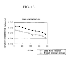
- Wafers were sliced from a hydrogen-doped crystal having a full length of 800 mm and grown at a constant pulling rate of 0.7 mm/min in an atmosphere having a hydrogen concentration of 6%, and the resistivities at various positions along the crystal were measured by the four-point probe test.
- the wafers were then subjected to 30 minutes of heat treatment at 650°C as donor killer (DK) treatment to extinguish thermal donors, following which the resistivities of the wafer were measured once again.
- DK donor killer
- FIG. 13 shows the impurity concentrations (thermal donor densities) calculated from the change in resistivity before and after DK treatment at various positions along the crystal. For the sake of reference, impurity concentrations for the case in which hydrogen was not supplied (non-doped) are also shown.
- silicon single crystal ingots were grown at a constant pulling rate of 0.7 mm/min and in an inert gas atmosphere having a hydrogen concentration (vol%) at one of six levels: 0. 1%, 3%, 6%, 10%, 20% and 0%. Silicon wafers sliced from each of the ingots were then prepared. Low temperature ramping heat treatment from 500 to 650°C was performed to each of the silicon wafers at a ramping rate of 0.3°C/min, following which 30 minutes of DK treatment at 650°C and one hour of high temperature heat treatment at 1200°C were performed.
- the silicon wafers in the examples according to the invention were able to suppress slip propagation much better than silicon wafers in the Comparative Example (Level 6).
- the hydrogen concentration in the inert gas atmosphere was 3% or more, it was possible to suppress the slip propagation to an invisible level.
- the entire region of the wafer is composed solely of an interstitial silicon-rich region. Hence, it is possible to obtain wafers in which the density and size of oxide precipitates and the DZ width are extremely homogeneous throughout the wafer plane.
- the present invention by combining hydrogen doping with the growth conditions of the grown-in defect-free crystal, it is possible to expand the pulling rate range for achieving a defect-free state. Therefore, the invention enables the stable growth of defect-free crystals, and remarkably improves the production yield of grown-in defect-free crystals.
Landscapes
- Chemical & Material Sciences (AREA)
- Engineering & Computer Science (AREA)
- Metallurgy (AREA)
- Crystallography & Structural Chemistry (AREA)
- Materials Engineering (AREA)
- Organic Chemistry (AREA)
- Physics & Mathematics (AREA)
- Condensed Matter Physics & Semiconductors (AREA)
- General Physics & Mathematics (AREA)
- Manufacturing & Machinery (AREA)
- Computer Hardware Design (AREA)
- Microelectronics & Electronic Packaging (AREA)
- Power Engineering (AREA)
- Thermal Sciences (AREA)
- Crystals, And After-Treatments Of Crystals (AREA)
Applications Claiming Priority (2)
| Application Number | Priority Date | Filing Date | Title |
|---|---|---|---|
| JP2005217647 | 2005-07-27 | ||
| PCT/JP2005/020548 WO2007013189A1 (fr) | 2005-07-27 | 2005-11-09 | Plaque de silicium et procédé de production de celle-ci |
Publications (2)
| Publication Number | Publication Date |
|---|---|
| EP1909315A1 true EP1909315A1 (fr) | 2008-04-09 |
| EP1909315A4 EP1909315A4 (fr) | 2008-11-26 |
Family
ID=37683097
Family Applications (1)
| Application Number | Title | Priority Date | Filing Date |
|---|---|---|---|
| EP05806093A Withdrawn EP1909315A4 (fr) | 2005-07-27 | 2005-11-09 | Plaque de silicium et procede de production de celle-ci |
Country Status (8)
| Country | Link |
|---|---|
| US (1) | US20070095274A1 (fr) |
| EP (1) | EP1909315A4 (fr) |
| JP (1) | JPWO2007013189A1 (fr) |
| KR (1) | KR100939299B1 (fr) |
| CN (1) | CN100565820C (fr) |
| DE (1) | DE05806093T1 (fr) |
| TW (1) | TWI310794B (fr) |
| WO (1) | WO2007013189A1 (fr) |
Cited By (1)
| Publication number | Priority date | Publication date | Assignee | Title |
|---|---|---|---|---|
| US8916425B2 (en) | 2010-07-26 | 2014-12-23 | Semiconductor Energy Laboratory Co., Ltd. | Method for forming microcrystalline semiconductor film and method for manufacturing semiconductor device |
Families Citing this family (18)
| Publication number | Priority date | Publication date | Assignee | Title |
|---|---|---|---|---|
| JP4432458B2 (ja) * | 2003-10-30 | 2010-03-17 | 信越半導体株式会社 | 単結晶の製造方法 |
| US20080292523A1 (en) | 2007-05-23 | 2008-11-27 | Sumco Corporation | Silicon single crystal wafer and the production method |
| JP5217245B2 (ja) * | 2007-05-23 | 2013-06-19 | 株式会社Sumco | シリコン単結晶ウェーハ及びその製造方法 |
| CN101942701A (zh) * | 2010-09-03 | 2011-01-12 | 浙江碧晶科技有限公司 | 一种太阳能级硅晶体的热处理方法 |
| CN102286784A (zh) * | 2011-08-19 | 2011-12-21 | 江西旭阳雷迪高科技股份有限公司 | 一种电阻率异常太阳能多晶硅片的处理方法 |
| CN102304764A (zh) * | 2011-09-19 | 2012-01-04 | 江西旭阳雷迪高科技股份有限公司 | 一种单晶硅片降低电阻值的处理方法 |
| JP2013163598A (ja) * | 2012-01-10 | 2013-08-22 | Globalwafers Japan Co Ltd | シリコンウェーハの製造方法 |
| CN102634850A (zh) * | 2012-03-31 | 2012-08-15 | 江苏鑫和泰光电科技有限公司 | 一种蓝宝石晶片的退火方法 |
| US9945048B2 (en) * | 2012-06-15 | 2018-04-17 | Taiwan Semiconductor Manufacturing Company, Ltd. | Semiconductor structure and method |
| JP6260100B2 (ja) * | 2013-04-03 | 2018-01-17 | 株式会社Sumco | エピタキシャルシリコンウェーハの製造方法 |
| KR101472349B1 (ko) * | 2013-05-21 | 2014-12-12 | 주식회사 엘지실트론 | 반도체용 실리콘 단결정 잉곳 및 웨이퍼 |
| US20150294868A1 (en) * | 2014-04-15 | 2015-10-15 | Infineon Technologies Ag | Method of Manufacturing Semiconductor Devices Containing Chalcogen Atoms |
| CN105543951B (zh) * | 2016-01-21 | 2019-01-01 | 浙江金瑞泓科技股份有限公司 | 一种在高COP硅单晶衬底上制备200mm-300mm低缺陷外延片的方法 |
| KR102032535B1 (ko) * | 2016-07-06 | 2019-10-15 | 가부시키가이샤 도쿠야마 | 단결정 실리콘 판상체 및 그의 제조 방법 |
| JP6699620B2 (ja) * | 2017-05-26 | 2020-05-27 | 株式会社Sumco | シリコン単結晶の製造方法 |
| EP3623801B1 (fr) * | 2018-09-14 | 2022-11-02 | Commissariat à l'Energie Atomique et aux Energies Alternatives | Procédé pour déterminer la concentration d'un donneur thermique d'un échantillon semi-conducteur |
| JP7230746B2 (ja) * | 2019-09-02 | 2023-03-01 | 株式会社Sumco | 単結晶シリコンの酸素濃度又は炭素濃度の測定方法 |
| JP7359241B2 (ja) | 2022-03-15 | 2023-10-11 | 株式会社Sumco | シリコン単結晶の製造方法 |
Citations (7)
| Publication number | Priority date | Publication date | Assignee | Title |
|---|---|---|---|---|
| US4437922A (en) * | 1982-03-26 | 1984-03-20 | International Business Machines Corporation | Method for tailoring oxygen precipitate particle density and distribution silicon wafers |
| JPS61178495A (ja) * | 1985-01-31 | 1986-08-11 | Fujitsu Ltd | 単結晶の成長方法 |
| JPH04298042A (ja) * | 1991-03-27 | 1992-10-21 | Komatsu Electron Metals Co Ltd | 半導体の熱処理方法 |
| JP2000281491A (ja) * | 1999-03-26 | 2000-10-10 | Nippon Steel Corp | シリコン半導体基板及びその製造方法 |
| US20010023941A1 (en) * | 2000-03-24 | 2001-09-27 | Wacker Siltronic Gesellschaft Fur Halbleitermaterialien Ag | Semiconductor wafer made from silicon and method for producing the semiconductor wafer |
| EP1138809A1 (fr) * | 1999-09-06 | 2001-10-04 | Shin-Etsu Handotai Co., Ltd | Plaquette et procede de fabrication de la plaquette |
| EP1551058A1 (fr) * | 2002-10-08 | 2005-07-06 | Shin-Etsu Handotai Co., Ltd | Tranche recuite et procede de fabrication de tranche recuite |
Family Cites Families (4)
| Publication number | Priority date | Publication date | Assignee | Title |
|---|---|---|---|---|
| US6045610A (en) * | 1997-02-13 | 2000-04-04 | Samsung Electronics Co., Ltd. | Methods of manufacturing monocrystalline silicon ingots and wafers by controlling pull rate profiles in a hot zone furnance |
| US6835245B2 (en) * | 2000-06-22 | 2004-12-28 | Sumitomo Mitsubishi Silicon Corporation | Method of manufacturing epitaxial wafer and method of producing single crystal as material therefor |
| JP4718668B2 (ja) * | 2000-06-26 | 2011-07-06 | 株式会社Sumco | エピタキシャルウェーハの製造方法 |
| JP2004111722A (ja) * | 2002-09-19 | 2004-04-08 | Toshiba Corp | 半導体装置 |
-
2005
- 2005-11-09 KR KR1020077028403A patent/KR100939299B1/ko active IP Right Grant
- 2005-11-09 CN CNB2005800502295A patent/CN100565820C/zh active Active
- 2005-11-09 JP JP2007526809A patent/JPWO2007013189A1/ja not_active Withdrawn
- 2005-11-09 WO PCT/JP2005/020548 patent/WO2007013189A1/fr active Application Filing
- 2005-11-09 DE DE05806093T patent/DE05806093T1/de active Pending
- 2005-11-09 EP EP05806093A patent/EP1909315A4/fr not_active Withdrawn
- 2005-11-16 TW TW094140334A patent/TWI310794B/zh active
-
2006
- 2006-05-26 US US11/441,352 patent/US20070095274A1/en not_active Abandoned
Patent Citations (7)
| Publication number | Priority date | Publication date | Assignee | Title |
|---|---|---|---|---|
| US4437922A (en) * | 1982-03-26 | 1984-03-20 | International Business Machines Corporation | Method for tailoring oxygen precipitate particle density and distribution silicon wafers |
| JPS61178495A (ja) * | 1985-01-31 | 1986-08-11 | Fujitsu Ltd | 単結晶の成長方法 |
| JPH04298042A (ja) * | 1991-03-27 | 1992-10-21 | Komatsu Electron Metals Co Ltd | 半導体の熱処理方法 |
| JP2000281491A (ja) * | 1999-03-26 | 2000-10-10 | Nippon Steel Corp | シリコン半導体基板及びその製造方法 |
| EP1138809A1 (fr) * | 1999-09-06 | 2001-10-04 | Shin-Etsu Handotai Co., Ltd | Plaquette et procede de fabrication de la plaquette |
| US20010023941A1 (en) * | 2000-03-24 | 2001-09-27 | Wacker Siltronic Gesellschaft Fur Halbleitermaterialien Ag | Semiconductor wafer made from silicon and method for producing the semiconductor wafer |
| EP1551058A1 (fr) * | 2002-10-08 | 2005-07-06 | Shin-Etsu Handotai Co., Ltd | Tranche recuite et procede de fabrication de tranche recuite |
Non-Patent Citations (2)
| Title |
|---|
| BISCHOFF B K ET AL: "ATTAINMENT OF EITHER A NARROW OR WIDE OXYGEN PRECIPITATE FREE ZONE IN SILICON WAFERS" IBM TECHNICAL DISCLOSURE BULLETIN, IBM CORP. NEW YORK, US, vol. 25, no. 6, 1 November 1982 (1982-11-01), page 2716/2717, XP000798858 ISSN: 0018-8689 * |
| See also references of WO2007013189A1 * |
Cited By (1)
| Publication number | Priority date | Publication date | Assignee | Title |
|---|---|---|---|---|
| US8916425B2 (en) | 2010-07-26 | 2014-12-23 | Semiconductor Energy Laboratory Co., Ltd. | Method for forming microcrystalline semiconductor film and method for manufacturing semiconductor device |
Also Published As
| Publication number | Publication date |
|---|---|
| JPWO2007013189A1 (ja) | 2009-02-05 |
| KR20080003937A (ko) | 2008-01-08 |
| CN100565820C (zh) | 2009-12-02 |
| WO2007013189A1 (fr) | 2007-02-01 |
| TW200704834A (en) | 2007-02-01 |
| KR100939299B1 (ko) | 2010-01-28 |
| DE05806093T1 (de) | 2008-08-21 |
| EP1909315A4 (fr) | 2008-11-26 |
| CN101238557A (zh) | 2008-08-06 |
| US20070095274A1 (en) | 2007-05-03 |
| TWI310794B (en) | 2009-06-11 |
Similar Documents
| Publication | Publication Date | Title |
|---|---|---|
| EP1909315A1 (fr) | Plaque de silicium et procede de production de celle-ci | |
| EP1785511B1 (fr) | Procede de croissance de monocristal de silicium | |
| US7637997B2 (en) | Silicon wafer, method for producing silicon wafer and method for growing silicon single crystal | |
| EP1881093B1 (fr) | Plaque de silicium monocristalline pour IGBT et son procédé de fabrication | |
| EP2110466B1 (fr) | Procédé de fabrication de silicium monocristallin | |
| JP6210125B2 (ja) | シリコン単結晶ウェーハ | |
| EP1143045B1 (fr) | Microplaquette epitaxiale, silicium monocristallin a cet effet et,procede de production | |
| JP2007022863A (ja) | シリコン単結晶の育成方法およびシリコンウェーハの製造方法 | |
| JP5250619B2 (ja) | シリコンウエハ及びシリコン結晶の製造方法 | |
| US20080292523A1 (en) | Silicon single crystal wafer and the production method | |
| JP4460671B2 (ja) | シリコン半導体基板及びその製造方法 | |
| EP1391921A1 (fr) | Procede de preparation d'une plaquette dopee a l'azote et recuite et plaquette dopee a l'azote et recuite | |
| JP5278324B2 (ja) | Igbt用シリコン単結晶ウェーハの製造方法 | |
| JPWO2009025342A1 (ja) | Igbt用のシリコン単結晶ウェーハ及びigbt用のシリコン単結晶ウェーハの製造方法 | |
| JP2005142434A (ja) | シリコン単結晶ウェーハの製造方法及びシリコン単結晶ウェーハ | |
| JP2003086597A (ja) | シリコン半導体基板およびその製造方法 | |
| JP5262021B2 (ja) | シリコンウェーハ及びその製造方法 | |
| JP2007242920A (ja) | 窒素ドープアニールウェーハの製造方法及び窒素ドープアニールウェーハ | |
| JP2009073684A (ja) | エピタキシャルウェーハの製造方法 | |
| JP2001240490A (ja) | 半導体シリコンウエーハの製造方法 |
Legal Events
| Date | Code | Title | Description |
|---|---|---|---|
| PUAI | Public reference made under article 153(3) epc to a published international application that has entered the european phase |
Free format text: ORIGINAL CODE: 0009012 |
|
| 17P | Request for examination filed |
Effective date: 20071114 |
|
| AK | Designated contracting states |
Kind code of ref document: A1 Designated state(s): DE |
|
| DET | De: translation of patent claims | ||
| RBV | Designated contracting states (corrected) |
Designated state(s): DE |
|
| A4 | Supplementary search report drawn up and despatched |
Effective date: 20081027 |
|
| 17Q | First examination report despatched |
Effective date: 20090211 |
|
| DAX | Request for extension of the european patent (deleted) | ||
| STAA | Information on the status of an ep patent application or granted ep patent |
Free format text: STATUS: THE APPLICATION IS DEEMED TO BE WITHDRAWN |
|
| 18D | Application deemed to be withdrawn |
Effective date: 20120601 |