EP1903608B1 - Festkörperbildsensor - Google Patents
Festkörperbildsensor Download PDFInfo
- Publication number
- EP1903608B1 EP1903608B1 EP06746502.1A EP06746502A EP1903608B1 EP 1903608 B1 EP1903608 B1 EP 1903608B1 EP 06746502 A EP06746502 A EP 06746502A EP 1903608 B1 EP1903608 B1 EP 1903608B1
- Authority
- EP
- European Patent Office
- Prior art keywords
- region
- microlens
- lens
- photoelectric conversion
- image sensor
- Prior art date
- Legal status (The legal status is an assumption and is not a legal conclusion. Google has not performed a legal analysis and makes no representation as to the accuracy of the status listed.)
- Active
Links
Images


Classifications
-
- G—PHYSICS
- G02—OPTICS
- G02B—OPTICAL ELEMENTS, SYSTEMS OR APPARATUS
- G02B3/00—Simple or compound lenses
- G02B3/0006—Arrays
- G02B3/0012—Arrays characterised by the manufacturing method
- G02B3/0018—Reflow, i.e. characterized by the step of melting microstructures to form curved surfaces, e.g. manufacturing of moulds and surfaces for transfer etching
-
- H—ELECTRICITY
- H10—SEMICONDUCTOR DEVICES; ELECTRIC SOLID-STATE DEVICES NOT OTHERWISE PROVIDED FOR
- H10F—INORGANIC SEMICONDUCTOR DEVICES SENSITIVE TO INFRARED RADIATION, LIGHT, ELECTROMAGNETIC RADIATION OF SHORTER WAVELENGTH OR CORPUSCULAR RADIATION
- H10F39/00—Integrated devices, or assemblies of multiple devices, comprising at least one element covered by group H10F30/00, e.g. radiation detectors comprising photodiode arrays
- H10F39/10—Integrated devices
- H10F39/12—Image sensors
-
- G—PHYSICS
- G02—OPTICS
- G02B—OPTICAL ELEMENTS, SYSTEMS OR APPARATUS
- G02B5/00—Optical elements other than lenses
- G02B5/20—Filters
- G02B5/201—Filters in the form of arrays
-
- H—ELECTRICITY
- H10—SEMICONDUCTOR DEVICES; ELECTRIC SOLID-STATE DEVICES NOT OTHERWISE PROVIDED FOR
- H10F—INORGANIC SEMICONDUCTOR DEVICES SENSITIVE TO INFRARED RADIATION, LIGHT, ELECTROMAGNETIC RADIATION OF SHORTER WAVELENGTH OR CORPUSCULAR RADIATION
- H10F39/00—Integrated devices, or assemblies of multiple devices, comprising at least one element covered by group H10F30/00, e.g. radiation detectors comprising photodiode arrays
- H10F39/011—Manufacture or treatment of image sensors covered by group H10F39/12
- H10F39/024—Manufacture or treatment of image sensors covered by group H10F39/12 of coatings or optical elements
-
- H—ELECTRICITY
- H10—SEMICONDUCTOR DEVICES; ELECTRIC SOLID-STATE DEVICES NOT OTHERWISE PROVIDED FOR
- H10F—INORGANIC SEMICONDUCTOR DEVICES SENSITIVE TO INFRARED RADIATION, LIGHT, ELECTROMAGNETIC RADIATION OF SHORTER WAVELENGTH OR CORPUSCULAR RADIATION
- H10F39/00—Integrated devices, or assemblies of multiple devices, comprising at least one element covered by group H10F30/00, e.g. radiation detectors comprising photodiode arrays
- H10F39/80—Constructional details of image sensors
- H10F39/802—Geometry or disposition of elements in pixels, e.g. address-lines or gate electrodes
- H10F39/8023—Disposition of the elements in pixels, e.g. smaller elements in the centre of the imager compared to larger elements at the periphery
-
- H—ELECTRICITY
- H10—SEMICONDUCTOR DEVICES; ELECTRIC SOLID-STATE DEVICES NOT OTHERWISE PROVIDED FOR
- H10F—INORGANIC SEMICONDUCTOR DEVICES SENSITIVE TO INFRARED RADIATION, LIGHT, ELECTROMAGNETIC RADIATION OF SHORTER WAVELENGTH OR CORPUSCULAR RADIATION
- H10F39/00—Integrated devices, or assemblies of multiple devices, comprising at least one element covered by group H10F30/00, e.g. radiation detectors comprising photodiode arrays
- H10F39/80—Constructional details of image sensors
- H10F39/806—Optical elements or arrangements associated with the image sensors
- H10F39/8063—Microlenses
-
- G—PHYSICS
- G02—OPTICS
- G02B—OPTICAL ELEMENTS, SYSTEMS OR APPARATUS
- G02B3/00—Simple or compound lenses
- G02B3/0006—Arrays
- G02B3/0037—Arrays characterized by the distribution or form of lenses
-
- G—PHYSICS
- G02—OPTICS
- G02B—OPTICAL ELEMENTS, SYSTEMS OR APPARATUS
- G02B3/00—Simple or compound lenses
- G02B3/0006—Arrays
- G02B3/0037—Arrays characterized by the distribution or form of lenses
- G02B3/0056—Arrays characterized by the distribution or form of lenses arranged along two different directions in a plane, e.g. honeycomb arrangement of lenses
Definitions
- the present invention relates to a solid state image sensor having a microlens.
- the solid state image sensor has a photoelectric conversion part converting light received by a pixel to an electric signal, and in the solid state image sensor, a plurality of pixels are arranged in matrix, and signal lines and so on through which the electric signals of the photoelectric conversion parts of the respective pixels are read are arranged around the photoelectric conversion parts.
- Light entering from a subject via a lens of a video camera or an electronic camera using a solid state image sensor is imaged on the pixels arranged in matrix and is converted to the electric signals by the photoelectric conversion parts.
- a typical microlens is semispherical and its plane shape is circular, while a plane shape of a pixel is generally quadrangular, and thus the shape of the pixel and the plane shape of the microlens do not always match each other, so that the photoelectric conversion part has an area in which light is not fully condensed.
- a patent document 2 describes an art to make the plane shape of a microlens quadrangular or to make the plane shape of a pixel and the plane shape of a microlens polygonal.
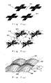
- Fig. 13(a) is a plane view of a typical solid state image sensor seen from above, where 701 denotes a quadrangular microlens according to a conventional art, 111 denotes a photoelectric conversion part such as a photodiode, 110 denotes a pixel among pixels arranged in matrix, A denotes a horizontal section position connecting centers of opposed sides of the pixel 110 and cutting the pixel 110 in a horizontal direction, and B denotes a diagonal section position cutting the pixel 110 in a diagonal direction.
- 701 denotes a quadrangular microlens according to a conventional art
- 111 denotes a photoelectric conversion part such as a photodiode
- 110 denotes a pixel among pixels arranged in matrix
- A denotes a horizontal section position connecting centers of opposed sides of the pixel 110 and cutting the pixel 110 in a horizontal direction
- B denotes a diagonal section position cutting the pixel 110 in a diagonal direction.
- FIG. 13(b) and (c) are views showing section shapes of the microlens 701 and the photoelectric conversion part 111 and optical condensing images when they are cut along the horizontal section position A and the diagonal section position B, in which 309 denotes incoming lights and L1 denotes a thickness of the microlens 701.
- the diagonal section shape of the microlens 701 in Fig. 13(c) is longer than a horizontal section shape of the microlens 701 in Fig. 13(b) , and the photoelectric conversion part 111 cut along the diagonal section position B in Fig. 13(c) is also longer.
- a curvature radius becomes large in the diagonal section shape of the microlens 701 in Fig. 13(c) , which makes it difficult to fully condense light in the photoelectric conversion part 111.
- the solid state image sensor of the present invention even if the shape of a pixel is quadrangular, an focusing efficiency in four corners is improved and thus it is possible to obtain a good focusing efficiency, and therefore, even with the same amount of light, a signal output from a photoelectric conversion part is increased, and sensitivity of the solid state image sensor can be improved.
- FIG. 1 A first embodiment of the solid state image sensor of the present invention will be described in detail by using Fig. 1 and Figs. 2 .
- Fig. 1 is a plane view showing the state of the solid state image sensor according to the first embodiment of the present invention seen from above.
- 1 denotes the solid state image sensor
- 2 denotes photoelectric conversion parts each formed by a buried photodiode or the like
- 3 denotes vertical CCDs vertically forwarding electric charge of signal generated in the photoelectric conversion parts 2
- 4 denotes a horizontal CCD horizontally forwarding the electric charge of signal forwarded from the vertical CCDs 3
- 5 denotes an output amplifier
- 6 denotes pixels
- 60 denotes units of pixel in terms of an area where light is condensed.
- a microlens though not shown in Fig. 1 , is disposed above each of the photoelectric conversion parts 2 via a planarizing layer.
- Each of the pixels 6 has part of the photoelectric conversion part 2 and part of the vertical CCD 3, and the plural pixels 6 are two-dimensionally arranged.
- Each of the microlenses is disposed with its center aligned with a center of the photoelectric conversion part 2. Therefore, the unit of pixel is an area denoted by the reference numeral 60 if defined in terms of an area where light is condensed.
- the unit of pixel is shown as having a rectangular shape for easier understanding, but actually, the unit of pixel has a square shape, and in the following drawings, a square area where light is condensed is shown as the unit of pixel.
- An electrode for controlling the forwarding of the electric charge by the vertical CCDs 3 includes a first polysilicon electrode (not shown) and a second polysilicon electrode (not shown), similarly to that in a typical solid state image sensor of a CCD type. Further, peripheral circuits and so on for generating a driving pulse and the like are further included in the solid state image sensor 1, but are not shown in the drawings since they are not essential parts of the present invention. It should be noted that the present invention is not limited to the solid state image sensor of a CCD type, and the same effect of the present invention can also be obtained in solid state image sensors of a CMOS type and so on.
- FIGs. 2 are views showing the unit of pixel 60 in Fig. 1 in detail, Fig. 2(a) being a plane view of the unit of pixel 60 seen from above, Fig. 2(b) being a horizontal sectional view of the unit of pixel 60 taken along a horizontal section position A in Fig. 2(a), and Fig. 2(c) being a diagonal sectional view of the unit of pixel 60 taken along a diagonal section position B in Fig. 2(a) .
- Figs. 2 are views showing the unit of pixel 60 in Fig. 1 in detail, Fig. 2(a) being a plane view of the unit of pixel 60 seen from above, Fig. 2(b) being a horizontal sectional view of the unit of pixel 60 taken along a horizontal section position A in Fig. 2(a), and Fig. 2(c) being a diagonal sectional view of the unit of pixel 60 taken along a diagonal section position B in Fig. 2(a) .
- Figs. 2 are views
- 101 denotes the microlens
- 102 denotes a planarizing layer under the microlens 101
- 103 denotes a color filter
- 104 denotes a shading film serving also as a power supply wiring
- 105 denotes a wiring
- 106 denotes a shading film
- 107 denotes a semiconductor substrate
- 108 denotes a planarizing layer between the photoelectric conversion part 111 and the color filter 103
- 109 denotes concave parts of the planarizing layer 102
- L1 denotes a thickness of the microlens 101 on a part other than the concave parts 109 of the planarizing layer 102
- L2 denotes a thickness of the microlens 101 on the concave parts 109 of the planarizing layer 102
- W1 denotes a thickness of the part other than the concave parts 109 of the planarizing layer 102
- W2 denotes a thickness of the concave
- the microlens 101 works as a lens with the thickness L1
- the microlens 101 works as a lens with the thickness L2 since, in four corners of the planarizing layer 102 and the microlens 101, the thickness of the planarizing layer 102 is W2 smaller than the thickness W1.
- the microlens 101 and the planarizing layer 102 are substantially equal in refractive index since the former is formed of, for example, a photoresist and the latter is formed of, for example, acrylic family resin, and hence, the microlens 101 and the planarizing layer 102 can be recognized as an integrated lens.
- Figs. 13 and Figs. 12 show an optical condensing condition in a case where the lens thickness in Figs. 13(b) and (c) is L1
- Figs. 12 show an optical condensing condition in a case where a microlens 121 whose lens thickness is L2 larger than the thickness L1 is used.
- Fig. 12(a) shows a horizontal section shape of the microlens 121 with the thickness L2
- Fig. 12(b) shows a diagonal section shape of the microlens 121 with the thickness L2, in both of which the same components as those in Figs. 13 are denoted by the same reference numerals used in Figs. 13 .
- the thickness of the microlens 701 is set to L1 for efficient optical condensing by the horizontal section shape as shown in Fig. 13(b)
- optical condensing by the diagonal section shape becomes poorer as shown in Fig. 13(c) .
- the thickness of the microlens 121 is set to the thickness L2 larger than L1 for efficient optical condensing by the diagonal section shape as shown in Fig. 12(b)
- a curvature radius becomes excessively small, and consequently, optical condensing by the horizontal section shape becomes poor as shown in Fig. 12(a) , so that it is not possible to fully condense incoming lights 309 in the photoelectric conversion part 111.
- the microlens 102 works as the microlens 701 with the thickness L1 in Fig. 13(b) and along the diagonal section position B, the microlens 102 works as the microlens 121 with the thickness L2 in Fig. 12(b) , which makes it possible to realize good optical condensing conditions as shown in Fig. 13(b) and Fig. 12(b) both along the horizontal sectional position A and along the diagonal sectional position B.
- the shape of the microlens 101 is shown in a perspective view in Fig. 3(a) .
- a microlens 201 in Fig. 3(b) is formed by modifying the above-described microlens 101 so that its four corners are rounded, and an effect of lens near the four corners are almost the same and therefore, the same effect can be obtained by this shape.
- the planarizing layer 102 has a double-level structure with the thickness W1 and the thickness W2, but the same effect can be obtained by the planarizing layer 102 with a multi-level structure and by the planarizing layer 102 with continuous inclinations.
- Such a shape can be realized by a conventionally known typical processing method such as etching, and for example, in the first embodiment, such a shape can be realized in such a manner that the planarizing layer 102 with the thickness W1 is first formed and then its periphery is removed by etching with its center part masked, and repeating this process enables the processing of the planarizing layer 102 into a multi-level structure.
- Another possible method to form a planarizing layer with two levels or more may be, Instead of processing the planarizing layer 102 as one thick planarizing layer, to process planarizing layers on the respective levels and accumulate these planarizing layers.
- the microlens 101 can also be realized by a conventionally known processing method, and for example, in the first embodiment, after the planarizing layer 102 having the thicknesses W1 and W2 is formed, a layer made of a photoresist or the like which is a base material of the microlens 10 is put over-the planarizing layer 102, and is heated by reflow or the like, and as a result, this layer flows down to enter low-level parts with W2 of the planarizing layer 102, whereby the microlens 101 can be formed.
- the solid state image sensor of the present invention even if the shape of a pixel is quadrangular, an focusing efficiency in four corners is improved and a solid state image sensor capable of having a good focusing efficiency can be provided, and consequently, signal output from a photoelectric conversion part is increased even with the same amount of light, enabling improved sensitivity of the solid state image sensor.
- Fig. 4(a) is a plane view of a unit of pixel 60 of the solid state image sensor of the present invention seen from above
- Fig. 4(b) is a horizontal sectional view of the unit of pixel 60 of the solid state image sensor having a microlens, taken along a horizontal section position A in Fig. 4(a)
- Fig. 4(c) is a diagonal sectional view of the unit of pixel 60 of the solid state image sensor, taken along a diagonal section position B in Fig. 4(a) .
- 302 denotes the microlens
- 301 denotes concave parts (to be described in detail in Figs. 5 )
- 303 denotes a horizontal lens shape of the microlens 302 taken along the horizontal section position A
- 304 denotes a diagonal lens shape of the microlens 302 taken along the diagonal section position B
- 305 denotes a planarizing layer
- 306 denotes an apex position of the microlens 302
- 307 denotes a lowest position of the horizontal lens shape 303
- 308 denotes a lowest position of the diagonal lens shape 304
- T denotes the maximum thickness of the microlens 302 from a microlens 302 side surface of the planarizing layer 305
- S1 denotes a difference in thickness between the lowest position 308 and the apex position 306 of the diagonal lens shape 304
- S2 denotes a difference in thickness between the lowest position 307 and the
- the microlens 302 has the lens thickness S2 smaller than the lens thickness S1
- the microlens 302 has the lens thickness S1 larger than the lens thickness S2. That is, where the horizontal section position A, the microlens 302 works as a lens having the horizontal section shape of the microlens 701 in Fig. 13(b) with the small thickness L1, and where the diagonal section position B, it works as a lens having the diagonal section shape of the microlens 121 in Fig. 12(b) with the large thickness L2, and therefore, it is possible to realize good optical condensing conditions as shown in Fig. 13(b) and Fig. 12(b) both along the horizontal section position A and along the diagonal section position B.
- Figs. 5 are explanatory views showing the state of the molding into the diagonal lens shape 304 in a view taken along the diagonal section position B shown in Fig. 4(c)
- Fig. 5(a) being a view in which a positional relation with a photoresist layer 401 as a base material of the microlens 302 is shown in an easily understandable manner in contrast to the diagonal section position B in Figs.
- Fig. 6(a) is a view showing a positional relation with the photoresist layer 401 along the horizontal section position A in Figs. 4 in a contrast manner, and since the photoresist layer 401 along the horizontal section position A does not include the concave part 301, its thickness is even without any concave. Applying reflow in this state softens the photoresist layer 401, so that each part of a dashed-line circle 501 gets gradually dented, though not shown in Fig. 6(b) , so that the shape of the photoresist layer 401 changes into the shape of the photoresist layer 402.
- Figs. 7 are explanatory views schematically depicting how the concave parts 301 deform by the application of the reflow.
- the concave parts 301 Prior to the application of the reflow, the concave parts 301 are geometrically cut off by etching or the like as shown in Fig. 7(a) , but applying heat by the reflow softens the photoresist layer 401 and its corner portions begin to flow down to become rounded in the manner of the dotted arrows as shown in Fig. 7(b) , and in particular, each portion of the dashed-line circle 501 in Fig. 7(b) begins to be dented, being pulled by the concave parts 301 on both sides.
- Fig. 7(c) shows the lens shape in wireframe, and along the horizontal section position A, the reflow does not make the lens bottom completely flat relative to the maximum thickness T of the lens apex positions 306; and at the lowest positions 307 of the horizontal lens shape 303, the thickness is larger than the thickness of four corner portions which are the lowest positions 308 of the diagonal lens shape 304, by the thickness U of the lowest positions 307, so that the microlens works as a lens with the thickness S2.
- the thickness of the microlens 302 along the horizontal section position A and the thickness of the microlens 302 along the diagonal section position B are different, and the microlens 302 along the horizontal section position A works as a thin lens with the thickness L1 of the microlens 701 shown in Fig. 13(b) , and the microlens 302 along the diagonal section position B works as a thick lens with the thickness L2 of the microlens 121 shown in Fig. 12(b) , and therefore, it is possible to realize good optical condensing conditions as shown in Fig. 13(b) and Fig. 12(b) both along the horizontal section position A and along the diagonal section position B.
- Fig. 8(a) is a plane view of a unit of pixel 60 of the solid state image sensor of the present invention seen from above
- Fig. 8(b) is a horizontal sectional view of the unit of pixel 60 of the solid state image sensor taken along a horizontal section position A in Fig. 8(a)
- Fig. 8(c) is a diagonal sectional view of the unit of pixel 60 of the solid state image sensor taken along a diagonal section position B in Fig. 8(a) .
- 701 denotes a microlens
- 702 denotes a second lens
- 703 and 704 denote planarizing layers
- 705 denotes slanting parts (to be described in detail later) of the second lens 702
- 706 denotes concave parts (to be described in detail later) of the second lens 702.
- the microlens 701 is a typical quadrangular microlens described in the conventional art in Figs. 13 , but is molded so that the microlens 701 along the horizontal section position A condenses lights efficiently in the photoelectric conversion part 111 as described in the conventional art in Fig. 13(b) . Therefore, it is assumed that there arises a problem that along the diagonal section position B, sufficient optical condensing is not enabled in the vicinity of four corners of the photoelectric conversion part 111 as shown in Fig. 13(c) .
- the planarizing layers 703 and 704 are formed of, for example, oxide silicon or the like and have a refractive index of about 1.5, and the second lens 702 therebetween is formed of, for example, nitride silicon having a different refractive index and has a refractive index of about 2, and therefore, the second lens 702 works as a lens.
- the second lens 702 is formed to have a desired shape by a generally used processing method such as etching.
- Fig. 9(a) which is a perspective view of the second lens 702
- the second lens 702 does not vary in thickness and is only a planar layer, but along the position of the diagonal section position B, has inclinations at corner portions thereof, and thus has an effect of lens in these portions.
- a sectional view of the second lens 702 taken along the horizontal section position A in Fig. 9(a) is shown in Fig. 10(a)
- a sectional view of the second lens 702 taken along the diagonal section position B in Fig. 9(a) is shown in Fig. 10(b) .
- the second lens 702 is formed on the planarizing layer 703, but the second lens 702 is a flat layer and does not work as a lens. That is, along the horizontal section position A, only the microlens 701 contributes to optical condensing in the photoelectric conversion part 111, and therefore, efficient optical condensing in the photoelectric conversion part 111 is made possible as shown in Fig. 13(b) .
- the second lens 702 is formed on the planarizing layer 703, but the layer of the second lens 702 does not exist at portions positioning in the concave parts 706 in Figs. 8 , and in areas of slanting parts 705 excluding the concave parts 706 in Figs. 8 , the layer of the second lens 702 is slanted so as to get gradually thinner toward the concave parts 706. That is, the second lens 702 has an effect of lens only near the slanting four corners, even though its portions excluding the concave parts 706 and the slanting parts 705 are substantially flat and thus have almost no effect of lens.
- the combination of optical condensing by the microlens 701 and optical condensing by the effect of lens of the four corner portions of the second lens 702 contribute to optical condensing in the photoelectric conversion part 111, and therefore, though, only with the microlens 701, efficient optical condensing in four corner portions of the photoelectric conversion part 111 is not possible as shown in Fig 13(c) , this is corrected by the effect of lens of the four corner portions of the second lens 702, resulting in two-stage optical condensing as shown in Figs. 11 , which enables efficient optical condensing in the photoelectric conversion part 111.
- the second lens 702 of the third embodiment has a shape with the four corners being cut off along straight lines as shown in Fig. 9(a) , but the second lens 702 having a shape with rounded corners as shown in Fig. 9(b) have the same effect of lens near the four corners, and thus can provide the same effect as that of the third embodiment.
Landscapes
- Physics & Mathematics (AREA)
- General Physics & Mathematics (AREA)
- Optics & Photonics (AREA)
- Engineering & Computer Science (AREA)
- Manufacturing & Machinery (AREA)
- Chemical & Material Sciences (AREA)
- Crystallography & Structural Chemistry (AREA)
- Solid State Image Pick-Up Elements (AREA)
- Transforming Light Signals Into Electric Signals (AREA)
Claims (8)
- Festkörper-Bildsensor, der Folgendes umfasst:ein Pixel (60), das auf einem Halbleitersubstrat ausgebildet ist;einen fotoelektrischen Umwandlungsteil (111), der in dem Pixel angeordnet ist, zum Umwandeln von Licht in ein elektrisches Signal; undeine Mikrolinse (101, 102), die über dem fotoelektrischen Umwandlungsteil (111) angeordnet ist,dadurch gekennzeichnet, dassdie Mikrolinse (101, 102) - von oben betrachtet, wenn eine direkte Entfernung von einer Mitte zu einem Linsenrand variiert wird - eine Ebenenform hat, wobei die Ebenenform, von oben betrachtet, ein Viereck mit gerundeten vier Ecken ist;die Mikrolinse (101, 102) eine erste Basisregion und eine zweite Basisregion, die nicht die erste Basisregion enthält, aufweist, wobei die erste Basisregion nahe den vier Ecken des Vierecks angeordnet ist und die zweite Basisregion vier Seiten des Vierecks enthält; undeine vertikale Höhe der ersten Basisregion von einer Oberseite des fotoelektrischen Umwandlungsteils (111) geringer ist als eine vertikale Höhe der zweiten Basisregion von der Oberseite des fotoelektrischen Umwandlungsteils (111).
- Festkörper-Bildsensor nach Anspruch 1, wobei die vertikale Höhe von der Oberseite des fotoelektrischen Umwandlungsteils (111) von der zweiten Basisregion in Richtung der ersten Basisregion schrittweise abnimmt.
- Festkörper-Bildsensor nach Anspruch 1, wobei
die vertikale Höhe von der Oberseite des fotoelektrischen Umwandlungsteils (111) von der zweiten Basisregion zu der ersten Basisregion kontinuierlich abnimmt. - Festkörper-Bildsensor nach einem der Ansprüche 1 bis 3, wobei
eine Planarisierungsschicht (102) zwischen dem fotoelektrischen Umwandlungsteil (111) und der Mikrolinse (101, 102) angeordnet ist; wobei
die Planarisierungsschicht eine erste Region und eine zweite Region, die nicht die erste Region enthält, aufweist, wobei die erste Region der ersten Basisregion, die sich nahe den vier Ecken des Vierecks befindet, auf die die Ebenentorm - von oben betrachtet - des Vierecks mit den gerundeten vier Ecken der Mikrolinse (101, 102) vertikal projiziert wird, gegenüberliegt und die zweite Oberseite der zweiten Basisregion, die die vier Seiten des Vierecks enthält, gegenüberliegt; und
eine Dicke der Planarisierungsschicht in der zweiten Region in Richtung einer Mikrolinsenseite größer ist als in der ersten Region. - Festkörper-Bildsensor nach Anspruch 4, wobei die Dicke der Planarisierungsschicht von der zweiten Region in Richtung der ersten Region schrittweise abnimmt.
- Festkörper-Bildsensor nach Anspruch 4, wobei
die Dicke der Planarisierungsschicht von der zweiten Region in Richtung der ersten Region kontinuierlich abnimmt. - Festkörper-Bildsensor, der Folgendes umfasst:ein Pixel (60), das auf einem Halbleitersubstrat ausgebildet ist;einen fotoelektrischen Umwandlungsteil (111), der in dem Pixel angeordnet ist, zum Umwandeln von Licht in ein elektrisches Signal; undeine Mikrolinse (701), die über dem fotoelektrischen Umwandlungsteil (111) angeordnet ist,dadurch gekennzeichnet, dassdie Mikrolinse (701) - von oben betrachtet, wenn eine direkte Entfernung von einer Mitte zu einem Linsenrand variiert wird - eine Ebenenform hat,eine Planarisierungsschicht (703, 704) zwischen dem fotoelektrischen Umwandlungsteil (111) und der Mikrolinse (701) angeordnet ist, wobei:in der Planarisierungsschicht (703, 704) eine zweite Linse (702) parallel zu dem fotoelektrischen Umwandlungsteil (111) angeordnet ist, wobei eine optische Achse der zweiten Linse (702) auf eineoptische Achse der Mikrolinse (701) ausgerichtet ist; unddie zweite Linse (702) - von oben betrachtet, wenn eine direkte Entfernung von einer Mitte zu einem Linsenrand variiert wird - eine Ebenenform hat, wobei die Ebenenform, von oben betrachtet, ein Viereck mit abgeschnittenen oder gerundeten vier Ecken ist und aus einem Element besteht, dessen Brechungsindex größer ist als der Brechungsindex der Planarisierungsschicht (703, 704), wobei:die zweite Linse (702) eine erste Region und eine zweite Region, die nicht die erste Region enthält, aufweist, und die zweite Region so geneigt ist, dass sie von der zweiten Region zu vier Ecken der zweiten Linse (702, 707), die die erste Region sind, dünner wird, wobei die erste Region nahe den vier Ecken des Vierecks angeordnet ist und die zweite Region die vier Seiten des Vierecks enthält.
- Festkörper-Bildsensor nach Anspruch 7, wobei:die zweite Region im Wesentlichen planar ist; unddie erste Region in der zweiten Linse so geneigt ist, dass ihre Dicke von Abschnitten neben der zweiten Region in Richtung der ersten Region in den vier Ecken der zweiten Linse kleiner wird.
Applications Claiming Priority (2)
| Application Number | Priority Date | Filing Date | Title |
|---|---|---|---|
| JP2005200296 | 2005-07-08 | ||
| PCT/JP2006/309799 WO2007007467A1 (ja) | 2005-07-08 | 2006-05-17 | 固体撮像素子 |
Publications (3)
| Publication Number | Publication Date |
|---|---|
| EP1903608A1 EP1903608A1 (de) | 2008-03-26 |
| EP1903608A4 EP1903608A4 (de) | 2011-12-14 |
| EP1903608B1 true EP1903608B1 (de) | 2013-04-24 |
Family
ID=37636867
Family Applications (1)
| Application Number | Title | Priority Date | Filing Date |
|---|---|---|---|
| EP06746502.1A Active EP1903608B1 (de) | 2005-07-08 | 2006-05-17 | Festkörperbildsensor |
Country Status (7)
| Country | Link |
|---|---|
| US (1) | US8013927B2 (de) |
| EP (1) | EP1903608B1 (de) |
| JP (1) | JP5104306B2 (de) |
| KR (1) | KR101294470B1 (de) |
| CN (1) | CN100570877C (de) |
| TW (1) | TW200715840A (de) |
| WO (1) | WO2007007467A1 (de) |
Families Citing this family (17)
| Publication number | Priority date | Publication date | Assignee | Title |
|---|---|---|---|---|
| KR20090102089A (ko) | 2008-03-25 | 2009-09-30 | 삼성전자주식회사 | 오디오 신호를 무선으로 전송하는 오디오 기기 및 전송방법 |
| JP5352392B2 (ja) * | 2009-09-14 | 2013-11-27 | 富士フイルム株式会社 | ウェハレベルレンズアレイの製造方法、ウェハレベルレンズアレイ、レンズモジュール及び撮像ユニット |
| CN102129106B (zh) * | 2010-01-20 | 2013-07-10 | 智宝科技股份有限公司 | 光学模块及其制作方法 |
| JP2014089432A (ja) * | 2012-03-01 | 2014-05-15 | Sony Corp | 固体撮像装置、固体撮像装置におけるマイクロレンズの形成方法、及び、電子機器 |
| WO2014003853A1 (en) | 2012-06-26 | 2014-01-03 | Biodesix, Inc. | Mass-spectral method for selection, and de-selection, of cancer patients for treatment with immune response generating therapies |
| JP6099345B2 (ja) * | 2012-09-27 | 2017-03-22 | シャープ株式会社 | レンズおよびその製造方法、固体撮像素子、電子情報機器 |
| US9077879B2 (en) * | 2013-01-09 | 2015-07-07 | Aac Acoustic Technologies (Shenzhen) Co., Ltd. | Array camera |
| US20140197508A1 (en) * | 2013-01-17 | 2014-07-17 | United Microelectronics Corporation | Image sensor and method for fabricating the same |
| US9547231B2 (en) * | 2013-06-12 | 2017-01-17 | Avago Technologies General Ip (Singapore) Pte. Ltd. | Device and method for making photomask assembly and photodetector device having light-collecting optical microstructure |
| JP6492396B2 (ja) * | 2013-12-06 | 2019-04-03 | 株式会社ニコン | 撮像素子および撮像装置 |
| JP6492395B2 (ja) * | 2013-12-06 | 2019-04-03 | 株式会社ニコン | 撮像素子および撮像装置 |
| US9620855B2 (en) | 2015-07-20 | 2017-04-11 | Elwha Llc | Electromagnetic beam steering antenna |
| US9577327B2 (en) | 2015-07-20 | 2017-02-21 | Elwha Llc | Electromagnetic beam steering antenna |
| CN112313799B (zh) * | 2018-06-29 | 2025-06-13 | 索尼半导体解决方案公司 | 固态成像装置、电子设备和制造固态成像装置的方法 |
| JP2019106548A (ja) * | 2019-03-07 | 2019-06-27 | 株式会社ニコン | 固体撮像素子および撮像装置 |
| JP2019134170A (ja) * | 2019-03-07 | 2019-08-08 | 株式会社ニコン | 撮像素子および撮像装置 |
| CN209640880U (zh) * | 2019-04-10 | 2019-11-15 | 深圳市汇顶科技股份有限公司 | 光学指纹识别装置和电子设备 |
Family Cites Families (59)
| Publication number | Priority date | Publication date | Assignee | Title |
|---|---|---|---|---|
| JPS6059752A (ja) | 1983-09-13 | 1985-04-06 | Nec Corp | 半導体装置の製造方法 |
| US4694185A (en) * | 1986-04-18 | 1987-09-15 | Eastman Kodak Company | Light sensing devices with lenticular pixels |
| KR960000223B1 (ko) * | 1990-11-16 | 1996-01-03 | 가부시키가이샤 도시바 | 고체촬상장치 및 그 제조방법 |
| JP2825702B2 (ja) * | 1992-05-20 | 1998-11-18 | シャープ株式会社 | 固体撮像素子 |
| JP2833941B2 (ja) * | 1992-10-09 | 1998-12-09 | 三菱電機株式会社 | 固体撮像装置とその製造方法 |
| US6166768A (en) * | 1994-01-28 | 2000-12-26 | California Institute Of Technology | Active pixel sensor array with simple floating gate pixels |
| US6021172A (en) * | 1994-01-28 | 2000-02-01 | California Institute Of Technology | Active pixel sensor having intra-pixel charge transfer with analog-to-digital converter |
| US5841126A (en) * | 1994-01-28 | 1998-11-24 | California Institute Of Technology | CMOS active pixel sensor type imaging system on a chip |
| US5949483A (en) * | 1994-01-28 | 1999-09-07 | California Institute Of Technology | Active pixel sensor array with multiresolution readout |
| US6486503B1 (en) * | 1994-01-28 | 2002-11-26 | California Institute Of Technology | Active pixel sensor array with electronic shuttering |
| US6570617B2 (en) * | 1994-01-28 | 2003-05-27 | California Institute Of Technology | CMOS active pixel sensor type imaging system on a chip |
| US5471515A (en) * | 1994-01-28 | 1995-11-28 | California Institute Of Technology | Active pixel sensor with intra-pixel charge transfer |
| AU1074797A (en) * | 1995-11-07 | 1997-06-05 | California Institute Of Technology | Capacitively coupled successive approximation ultra low power analog-to-digital converter |
| US5793322A (en) * | 1995-11-07 | 1998-08-11 | California Institute Of Technology | Successive approximation analog-to-digital converter using balanced charge integrating amplifiers |
| US6115065A (en) * | 1995-11-07 | 2000-09-05 | California Institute Of Technology | Image sensor producing at least two integration times from each sensing pixel |
| US5990506A (en) * | 1996-03-20 | 1999-11-23 | California Institute Of Technology | Active pixel sensors with substantially planarized color filtering elements |
| US5929800A (en) * | 1996-08-05 | 1999-07-27 | California Institute Of Technology | Charge integration successive approximation analog-to-digital converter for focal plane applications using a single amplifier |
| US5886659A (en) * | 1996-08-21 | 1999-03-23 | California Institute Of Technology | On-focal-plane analog-to-digital conversion for current-mode imaging devices |
| KR100223853B1 (ko) * | 1996-08-26 | 1999-10-15 | 구본준 | 고체촬상소자의 구조 및 제조방법 |
| US5952645A (en) * | 1996-08-27 | 1999-09-14 | California Institute Of Technology | Light-sensing array with wedge-like reflective optical concentrators |
| US6175383B1 (en) * | 1996-11-07 | 2001-01-16 | California Institute Of Technology | Method and apparatus of high dynamic range image sensor with individual pixel reset |
| US5887049A (en) * | 1996-11-12 | 1999-03-23 | California Institute Of Technology | Self-triggered X-ray sensor |
| US5909026A (en) * | 1996-11-12 | 1999-06-01 | California Institute Of Technology | Integrated sensor with frame memory and programmable resolution for light adaptive imaging |
| DE69715029D1 (de) * | 1996-11-12 | 2002-10-02 | California Inst Of Techn | Halbleiterbildsensor mit onchip-verschlüsselung |
| US6787749B1 (en) * | 1996-11-12 | 2004-09-07 | California Institute Of Technology | Integrated sensor with frame memory and programmable resolution for light adaptive imaging |
| JP3447510B2 (ja) * | 1997-04-09 | 2003-09-16 | Necエレクトロニクス株式会社 | 固体撮像素子、その製造方法及び固体撮像装置 |
| US6476860B1 (en) * | 1997-07-14 | 2002-11-05 | California Institute Of Technology | Center of mass detection via an active pixel sensor |
| US6515702B1 (en) * | 1997-07-14 | 2003-02-04 | California Institute Of Technology | Active pixel image sensor with a winner-take-all mode of operation |
| US6107619A (en) * | 1997-07-14 | 2000-08-22 | California Institute Of Technology | Delta-doped hybrid advanced detector for low energy particle detection |
| US6546148B1 (en) * | 1997-07-14 | 2003-04-08 | California Institute Of Technology | Circuitry for determining median of image portions |
| US6107618A (en) * | 1997-07-14 | 2000-08-22 | California Institute Of Technology | Integrated infrared and visible image sensors |
| US5903039A (en) * | 1997-07-15 | 1999-05-11 | Hewlett-Packard Company | Enhanced-light-collection-efficiency sensor |
| US6403963B1 (en) * | 1997-09-29 | 2002-06-11 | California Institute Of Technology | Delta-doped CCD's as low-energy particle detectors and imagers |
| US6606122B1 (en) * | 1997-09-29 | 2003-08-12 | California Institute Of Technology | Single chip camera active pixel sensor |
| US6801258B1 (en) * | 1998-03-16 | 2004-10-05 | California Institute Of Technology | CMOS integration sensor with fully differential column readout circuit for light adaptive imaging |
| JP2000039503A (ja) | 1998-07-22 | 2000-02-08 | Matsushita Electric Ind Co Ltd | レンズアレイ |
| US6373050B1 (en) * | 1998-10-07 | 2002-04-16 | California Institute Of Technology | Focal plane infrared readout circuit with automatic background suppression |
| WO2000021280A1 (en) * | 1998-10-07 | 2000-04-13 | California Institute Of Technology | Silicon-on-insulator (soi) active pixel sensors with the photosites implemented in the substrate |
| US6384413B1 (en) * | 1998-10-13 | 2002-05-07 | California Institute Of Technology | Focal plane infrared readout circuit |
| JP2000162406A (ja) | 1998-11-26 | 2000-06-16 | Toppan Printing Co Ltd | マイクロレンズ |
| US6326230B1 (en) * | 1999-01-06 | 2001-12-04 | California Institute Of Technology | High speed CMOS imager with motion artifact supression and anti-blooming |
| JP2001102556A (ja) * | 1999-09-27 | 2001-04-13 | Fuji Film Microdevices Co Ltd | 固体撮像装置 |
| KR100457283B1 (ko) * | 1999-09-30 | 2004-11-16 | 캘리포니아 인스티튜트 오브 테크놀로지 | 광다이오드형 cmos 이미저를 이용한 고속의 온 칩윈도우 센트로이드 계산 시스템 |
| US7268814B1 (en) * | 1999-10-05 | 2007-09-11 | California Institute Of Technology | Time-delayed-integration imaging with active pixel sensors |
| US6171885B1 (en) * | 1999-10-12 | 2001-01-09 | Taiwan Semiconductor Manufacturing Company | High efficiency color filter process for semiconductor array imaging devices |
| US6839452B1 (en) * | 1999-11-23 | 2005-01-04 | California Institute Of Technology | Dynamically re-configurable CMOS imagers for an active vision system |
| JP4123667B2 (ja) * | 2000-01-26 | 2008-07-23 | 凸版印刷株式会社 | 固体撮像素子の製造方法 |
| US6933488B2 (en) * | 2000-06-08 | 2005-08-23 | California Institute Of Technology | Variable electronic shutter in CMOS imager with improved anti smearing techniques |
| DE60136963D1 (de) * | 2000-11-16 | 2009-01-22 | California Inst Of Techn | Photodioden-cmos-abbildungsvorrichtung mit spaltenrückkopplungs-soft-reset |
| JP2003172804A (ja) | 2001-12-06 | 2003-06-20 | Matsushita Electric Ind Co Ltd | マイクロレンズアレイ及びその製造方法 |
| JP4383959B2 (ja) * | 2003-05-28 | 2009-12-16 | キヤノン株式会社 | 光電変換装置およびその製造方法 |
| JP3729353B2 (ja) * | 2003-06-18 | 2005-12-21 | 松下電器産業株式会社 | 固体撮像装置およびその製造方法 |
| US6995911B2 (en) * | 2003-06-26 | 2006-02-07 | Micron Technology, Inc. | Micro-lenses and structures for increasing area coverage and controlling shape of micro-lenses |
| JP2005072364A (ja) * | 2003-08-26 | 2005-03-17 | Fuji Film Microdevices Co Ltd | 固体撮像素子及びその製造方法 |
| US7443005B2 (en) * | 2004-06-10 | 2008-10-28 | Tiawan Semiconductor Manufacturing Co., Ltd. | Lens structures suitable for use in image sensors and method for making the same |
| EP1626442B1 (de) * | 2004-08-13 | 2011-01-12 | St Microelectronics S.A. | Bildsensor |
| US7453109B2 (en) * | 2004-09-03 | 2008-11-18 | Canon Kabushiki Kaisha | Solid-state image sensor and imaging system |
| JP2006145627A (ja) * | 2004-11-16 | 2006-06-08 | Sanyo Electric Co Ltd | マイクロレンズの製造方法及び固体撮像素子の製造方法 |
| JP2007180157A (ja) * | 2005-12-27 | 2007-07-12 | Fujifilm Corp | 固体撮像素子 |
-
2006
- 2006-05-17 EP EP06746502.1A patent/EP1903608B1/de active Active
- 2006-05-17 WO PCT/JP2006/309799 patent/WO2007007467A1/ja not_active Ceased
- 2006-05-17 CN CNB2006800249906A patent/CN100570877C/zh active Active
- 2006-05-17 JP JP2007524532A patent/JP5104306B2/ja active Active
- 2006-05-17 US US11/922,768 patent/US8013927B2/en active Active
- 2006-05-17 KR KR1020087000230A patent/KR101294470B1/ko active Active
- 2006-07-07 TW TW095124740A patent/TW200715840A/zh unknown
Also Published As
| Publication number | Publication date |
|---|---|
| JP5104306B2 (ja) | 2012-12-19 |
| CN100570877C (zh) | 2009-12-16 |
| CN101218677A (zh) | 2008-07-09 |
| JPWO2007007467A1 (ja) | 2009-01-29 |
| KR101294470B1 (ko) | 2013-08-07 |
| EP1903608A1 (de) | 2008-03-26 |
| US8013927B2 (en) | 2011-09-06 |
| US20090225205A1 (en) | 2009-09-10 |
| WO2007007467A1 (ja) | 2007-01-18 |
| TWI331874B (de) | 2010-10-11 |
| TW200715840A (en) | 2007-04-16 |
| KR20080027329A (ko) | 2008-03-26 |
| EP1903608A4 (de) | 2011-12-14 |
Similar Documents
| Publication | Publication Date | Title |
|---|---|---|
| EP1903608B1 (de) | Festkörperbildsensor | |
| US7427742B2 (en) | Microlens for use with a solid-state image sensor and a non-telecentric taking lens | |
| US7303931B2 (en) | Microfeature workpieces having microlenses and methods of forming microlenses on microfeature workpieces | |
| TWI636557B (zh) | 固體攝像裝置及其製造方法、以及電子機器 | |
| US11765476B2 (en) | Imaging element and method for manufacturing imaging element | |
| EP1557886A2 (de) | Festkörperbildaufnahmevorrichtung und Kamera | |
| CN101681916A (zh) | 形成于较大透镜阵列上的用于对像素群组内经移位的光电二极管位置进行调整的微透镜 | |
| JP2010118412A (ja) | 固体撮像装置及びその製造方法 | |
| JP2008547064A (ja) | 傾きのあるマイクロレンズの製造方法 | |
| JP2009289927A (ja) | 固体撮像装置及びその製造方法 | |
| US7560295B2 (en) | Methods for creating gapless inner microlenses, arrays of microlenses, and imagers having same | |
| JP2008052004A (ja) | レンズアレイ及び固体撮像素子の製造方法 | |
| KR102749178B1 (ko) | 이미지 센서 | |
| JP2009124053A (ja) | 光電変換装置及びその製造方法 | |
| JPH04343471A (ja) | 固体撮像素子 | |
| JP2000260969A (ja) | 固体撮像素子の製造方法 | |
| JP2000174244A (ja) | 固体撮像素子 | |
| JP4626255B2 (ja) | 固体撮像素子の製造方法 | |
| JP2000260970A (ja) | 固体撮像素子およびその製造方法 | |
| JP3049856B2 (ja) | 固体撮像素子 | |
| JP2006344656A (ja) | 固体撮像素子及びその製造方法 | |
| JP2019134170A (ja) | 撮像素子および撮像装置 | |
| JP2007201090A (ja) | 固体撮像素子 |
Legal Events
| Date | Code | Title | Description |
|---|---|---|---|
| PUAI | Public reference made under article 153(3) epc to a published international application that has entered the european phase |
Free format text: ORIGINAL CODE: 0009012 |
|
| 17P | Request for examination filed |
Effective date: 20071203 |
|
| AK | Designated contracting states |
Kind code of ref document: A1 Designated state(s): AT BE BG CH CY CZ DE DK EE ES FI FR GB GR HU IE IS IT LI LT LU LV MC NL PL PT RO SE SI SK TR |
|
| RAP1 | Party data changed (applicant data changed or rights of an application transferred) |
Owner name: NIKON CORPORATION |
|
| A4 | Supplementary search report drawn up and despatched |
Effective date: 20111116 |
|
| RIC1 | Information provided on ipc code assigned before grant |
Ipc: H04N 5/335 20110101ALI20111110BHEP Ipc: H01L 27/146 20060101AFI20111110BHEP |
|
| DAX | Request for extension of the european patent (deleted) | ||
| 17Q | First examination report despatched |
Effective date: 20120727 |
|
| REG | Reference to a national code |
Ref country code: DE Ref legal event code: R079 Ref document number: 602006035904 Country of ref document: DE Free format text: PREVIOUS MAIN CLASS: H01L0027140000 Ipc: H01L0027146000 |
|
| GRAP | Despatch of communication of intention to grant a patent |
Free format text: ORIGINAL CODE: EPIDOSNIGR1 |
|
| RIC1 | Information provided on ipc code assigned before grant |
Ipc: G02B 3/00 20060101ALI20121023BHEP Ipc: H04N 5/225 20060101ALI20121023BHEP Ipc: G02B 5/20 20060101ALI20121023BHEP Ipc: H01L 27/146 20060101AFI20121023BHEP Ipc: H04N 5/335 20110101ALI20121023BHEP |
|
| GRAS | Grant fee paid |
Free format text: ORIGINAL CODE: EPIDOSNIGR3 |
|
| GRAA | (expected) grant |
Free format text: ORIGINAL CODE: 0009210 |
|
| AK | Designated contracting states |
Kind code of ref document: B1 Designated state(s): AT BE BG CH CY CZ DE DK EE ES FI FR GB GR HU IE IS IT LI LT LU LV MC NL PL PT RO SE SI SK TR |
|
| REG | Reference to a national code |
Ref country code: GB Ref legal event code: FG4D |
|
| REG | Reference to a national code |
Ref country code: CH Ref legal event code: EP |
|
| REG | Reference to a national code |
Ref country code: AT Ref legal event code: REF Ref document number: 609070 Country of ref document: AT Kind code of ref document: T Effective date: 20130515 |
|
| REG | Reference to a national code |
Ref country code: IE Ref legal event code: FG4D |
|
| REG | Reference to a national code |
Ref country code: DE Ref legal event code: R096 Ref document number: 602006035904 Country of ref document: DE Effective date: 20130627 |
|
| REG | Reference to a national code |
Ref country code: AT Ref legal event code: MK05 Ref document number: 609070 Country of ref document: AT Kind code of ref document: T Effective date: 20130424 |
|
| REG | Reference to a national code |
Ref country code: LT Ref legal event code: MG4D |
|
| REG | Reference to a national code |
Ref country code: NL Ref legal event code: VDEP Effective date: 20130424 |
|
| PG25 | Lapsed in a contracting state [announced via postgrant information from national office to epo] |
Ref country code: FI Free format text: LAPSE BECAUSE OF FAILURE TO SUBMIT A TRANSLATION OF THE DESCRIPTION OR TO PAY THE FEE WITHIN THE PRESCRIBED TIME-LIMIT Effective date: 20130424 Ref country code: PT Free format text: LAPSE BECAUSE OF FAILURE TO SUBMIT A TRANSLATION OF THE DESCRIPTION OR TO PAY THE FEE WITHIN THE PRESCRIBED TIME-LIMIT Effective date: 20130826 Ref country code: IS Free format text: LAPSE BECAUSE OF FAILURE TO SUBMIT A TRANSLATION OF THE DESCRIPTION OR TO PAY THE FEE WITHIN THE PRESCRIBED TIME-LIMIT Effective date: 20130824 Ref country code: GR Free format text: LAPSE BECAUSE OF FAILURE TO SUBMIT A TRANSLATION OF THE DESCRIPTION OR TO PAY THE FEE WITHIN THE PRESCRIBED TIME-LIMIT Effective date: 20130725 Ref country code: AT Free format text: LAPSE BECAUSE OF FAILURE TO SUBMIT A TRANSLATION OF THE DESCRIPTION OR TO PAY THE FEE WITHIN THE PRESCRIBED TIME-LIMIT Effective date: 20130424 Ref country code: LT Free format text: LAPSE BECAUSE OF FAILURE TO SUBMIT A TRANSLATION OF THE DESCRIPTION OR TO PAY THE FEE WITHIN THE PRESCRIBED TIME-LIMIT Effective date: 20130424 Ref country code: BE Free format text: LAPSE BECAUSE OF FAILURE TO SUBMIT A TRANSLATION OF THE DESCRIPTION OR TO PAY THE FEE WITHIN THE PRESCRIBED TIME-LIMIT Effective date: 20130424 Ref country code: SE Free format text: LAPSE BECAUSE OF FAILURE TO SUBMIT A TRANSLATION OF THE DESCRIPTION OR TO PAY THE FEE WITHIN THE PRESCRIBED TIME-LIMIT Effective date: 20130424 Ref country code: SI Free format text: LAPSE BECAUSE OF FAILURE TO SUBMIT A TRANSLATION OF THE DESCRIPTION OR TO PAY THE FEE WITHIN THE PRESCRIBED TIME-LIMIT Effective date: 20130424 Ref country code: ES Free format text: LAPSE BECAUSE OF FAILURE TO SUBMIT A TRANSLATION OF THE DESCRIPTION OR TO PAY THE FEE WITHIN THE PRESCRIBED TIME-LIMIT Effective date: 20130804 |
|
| PG25 | Lapsed in a contracting state [announced via postgrant information from national office to epo] |
Ref country code: BG Free format text: LAPSE BECAUSE OF FAILURE TO SUBMIT A TRANSLATION OF THE DESCRIPTION OR TO PAY THE FEE WITHIN THE PRESCRIBED TIME-LIMIT Effective date: 20130724 Ref country code: LV Free format text: LAPSE BECAUSE OF FAILURE TO SUBMIT A TRANSLATION OF THE DESCRIPTION OR TO PAY THE FEE WITHIN THE PRESCRIBED TIME-LIMIT Effective date: 20130424 Ref country code: CY Free format text: LAPSE BECAUSE OF FAILURE TO SUBMIT A TRANSLATION OF THE DESCRIPTION OR TO PAY THE FEE WITHIN THE PRESCRIBED TIME-LIMIT Effective date: 20130424 Ref country code: PL Free format text: LAPSE BECAUSE OF FAILURE TO SUBMIT A TRANSLATION OF THE DESCRIPTION OR TO PAY THE FEE WITHIN THE PRESCRIBED TIME-LIMIT Effective date: 20130424 |
|
| REG | Reference to a national code |
Ref country code: CH Ref legal event code: PL |
|
| PG25 | Lapsed in a contracting state [announced via postgrant information from national office to epo] |
Ref country code: LI Free format text: LAPSE BECAUSE OF NON-PAYMENT OF DUE FEES Effective date: 20130531 Ref country code: MC Free format text: LAPSE BECAUSE OF FAILURE TO SUBMIT A TRANSLATION OF THE DESCRIPTION OR TO PAY THE FEE WITHIN THE PRESCRIBED TIME-LIMIT Effective date: 20130424 Ref country code: CZ Free format text: LAPSE BECAUSE OF FAILURE TO SUBMIT A TRANSLATION OF THE DESCRIPTION OR TO PAY THE FEE WITHIN THE PRESCRIBED TIME-LIMIT Effective date: 20130424 Ref country code: DK Free format text: LAPSE BECAUSE OF FAILURE TO SUBMIT A TRANSLATION OF THE DESCRIPTION OR TO PAY THE FEE WITHIN THE PRESCRIBED TIME-LIMIT Effective date: 20130424 Ref country code: CH Free format text: LAPSE BECAUSE OF NON-PAYMENT OF DUE FEES Effective date: 20130531 Ref country code: EE Free format text: LAPSE BECAUSE OF FAILURE TO SUBMIT A TRANSLATION OF THE DESCRIPTION OR TO PAY THE FEE WITHIN THE PRESCRIBED TIME-LIMIT Effective date: 20130424 Ref country code: SK Free format text: LAPSE BECAUSE OF FAILURE TO SUBMIT A TRANSLATION OF THE DESCRIPTION OR TO PAY THE FEE WITHIN THE PRESCRIBED TIME-LIMIT Effective date: 20130424 |
|
| REG | Reference to a national code |
Ref country code: IE Ref legal event code: MM4A |
|
| PG25 | Lapsed in a contracting state [announced via postgrant information from national office to epo] |
Ref country code: RO Free format text: LAPSE BECAUSE OF FAILURE TO SUBMIT A TRANSLATION OF THE DESCRIPTION OR TO PAY THE FEE WITHIN THE PRESCRIBED TIME-LIMIT Effective date: 20130424 Ref country code: NL Free format text: LAPSE BECAUSE OF FAILURE TO SUBMIT A TRANSLATION OF THE DESCRIPTION OR TO PAY THE FEE WITHIN THE PRESCRIBED TIME-LIMIT Effective date: 20130424 Ref country code: IT Free format text: LAPSE BECAUSE OF FAILURE TO SUBMIT A TRANSLATION OF THE DESCRIPTION OR TO PAY THE FEE WITHIN THE PRESCRIBED TIME-LIMIT Effective date: 20130424 |
|
| PLBE | No opposition filed within time limit |
Free format text: ORIGINAL CODE: 0009261 |
|
| STAA | Information on the status of an ep patent application or granted ep patent |
Free format text: STATUS: NO OPPOSITION FILED WITHIN TIME LIMIT |
|
| 26N | No opposition filed |
Effective date: 20140127 |
|
| PG25 | Lapsed in a contracting state [announced via postgrant information from national office to epo] |
Ref country code: IE Free format text: LAPSE BECAUSE OF NON-PAYMENT OF DUE FEES Effective date: 20130517 |
|
| REG | Reference to a national code |
Ref country code: DE Ref legal event code: R097 Ref document number: 602006035904 Country of ref document: DE Effective date: 20140127 |
|
| PG25 | Lapsed in a contracting state [announced via postgrant information from national office to epo] |
Ref country code: TR Free format text: LAPSE BECAUSE OF FAILURE TO SUBMIT A TRANSLATION OF THE DESCRIPTION OR TO PAY THE FEE WITHIN THE PRESCRIBED TIME-LIMIT Effective date: 20130424 |
|
| PG25 | Lapsed in a contracting state [announced via postgrant information from national office to epo] |
Ref country code: LU Free format text: LAPSE BECAUSE OF NON-PAYMENT OF DUE FEES Effective date: 20130517 Ref country code: HU Free format text: LAPSE BECAUSE OF FAILURE TO SUBMIT A TRANSLATION OF THE DESCRIPTION OR TO PAY THE FEE WITHIN THE PRESCRIBED TIME-LIMIT; INVALID AB INITIO Effective date: 20060517 |
|
| REG | Reference to a national code |
Ref country code: FR Ref legal event code: PLFP Year of fee payment: 11 |
|
| REG | Reference to a national code |
Ref country code: FR Ref legal event code: PLFP Year of fee payment: 12 |
|
| REG | Reference to a national code |
Ref country code: FR Ref legal event code: PLFP Year of fee payment: 13 |
|
| REG | Reference to a national code |
Ref country code: FR Ref legal event code: PLFP Year of fee payment: 18 |
|
| P01 | Opt-out of the competence of the unified patent court (upc) registered |
Effective date: 20230517 |
|
| REG | Reference to a national code |
Ref country code: DE Ref legal event code: R079 Ref document number: 602006035904 Country of ref document: DE Free format text: PREVIOUS MAIN CLASS: H01L0027146000 Ipc: H10F0039180000 |
|
| PGFP | Annual fee paid to national office [announced via postgrant information from national office to epo] |
Ref country code: GB Payment date: 20250327 Year of fee payment: 20 |
|
| PGFP | Annual fee paid to national office [announced via postgrant information from national office to epo] |
Ref country code: DE Payment date: 20250402 Year of fee payment: 20 |
|
| PGFP | Annual fee paid to national office [announced via postgrant information from national office to epo] |
Ref country code: FR Payment date: 20250401 Year of fee payment: 20 |