EP1898255B1 - Method of manufacturing liquid crystal display - Google Patents
Method of manufacturing liquid crystal display Download PDFInfo
- Publication number
- EP1898255B1 EP1898255B1 EP07017301A EP07017301A EP1898255B1 EP 1898255 B1 EP1898255 B1 EP 1898255B1 EP 07017301 A EP07017301 A EP 07017301A EP 07017301 A EP07017301 A EP 07017301A EP 1898255 B1 EP1898255 B1 EP 1898255B1
- Authority
- EP
- European Patent Office
- Prior art keywords
- region
- layer
- forming
- photosensitive film
- data
- Prior art date
- Legal status (The legal status is an assumption and is not a legal conclusion. Google has not performed a legal analysis and makes no representation as to the accuracy of the status listed.)
- Active
Links
Images


Classifications
-
- G—PHYSICS
- G02—OPTICS
- G02F—OPTICAL DEVICES OR ARRANGEMENTS FOR THE CONTROL OF LIGHT BY MODIFICATION OF THE OPTICAL PROPERTIES OF THE MEDIA OF THE ELEMENTS INVOLVED THEREIN; NON-LINEAR OPTICS; FREQUENCY-CHANGING OF LIGHT; OPTICAL LOGIC ELEMENTS; OPTICAL ANALOGUE/DIGITAL CONVERTERS
- G02F1/00—Devices or arrangements for the control of the intensity, colour, phase, polarisation or direction of light arriving from an independent light source, e.g. switching, gating or modulating; Non-linear optics
- G02F1/01—Devices or arrangements for the control of the intensity, colour, phase, polarisation or direction of light arriving from an independent light source, e.g. switching, gating or modulating; Non-linear optics for the control of the intensity, phase, polarisation or colour
- G02F1/13—Devices or arrangements for the control of the intensity, colour, phase, polarisation or direction of light arriving from an independent light source, e.g. switching, gating or modulating; Non-linear optics for the control of the intensity, phase, polarisation or colour based on liquid crystals, e.g. single liquid crystal display cells
- G02F1/133—Constructional arrangements; Operation of liquid crystal cells; Circuit arrangements
- G02F1/136—Liquid crystal cells structurally associated with a semi-conducting layer or substrate, e.g. cells forming part of an integrated circuit
- G02F1/1362—Active matrix addressed cells
-
- G—PHYSICS
- G02—OPTICS
- G02F—OPTICAL DEVICES OR ARRANGEMENTS FOR THE CONTROL OF LIGHT BY MODIFICATION OF THE OPTICAL PROPERTIES OF THE MEDIA OF THE ELEMENTS INVOLVED THEREIN; NON-LINEAR OPTICS; FREQUENCY-CHANGING OF LIGHT; OPTICAL LOGIC ELEMENTS; OPTICAL ANALOGUE/DIGITAL CONVERTERS
- G02F1/00—Devices or arrangements for the control of the intensity, colour, phase, polarisation or direction of light arriving from an independent light source, e.g. switching, gating or modulating; Non-linear optics
- G02F1/01—Devices or arrangements for the control of the intensity, colour, phase, polarisation or direction of light arriving from an independent light source, e.g. switching, gating or modulating; Non-linear optics for the control of the intensity, phase, polarisation or colour
- G02F1/13—Devices or arrangements for the control of the intensity, colour, phase, polarisation or direction of light arriving from an independent light source, e.g. switching, gating or modulating; Non-linear optics for the control of the intensity, phase, polarisation or colour based on liquid crystals, e.g. single liquid crystal display cells
- G02F1/133—Constructional arrangements; Operation of liquid crystal cells; Circuit arrangements
- G02F1/136—Liquid crystal cells structurally associated with a semi-conducting layer or substrate, e.g. cells forming part of an integrated circuit
-
- G—PHYSICS
- G02—OPTICS
- G02F—OPTICAL DEVICES OR ARRANGEMENTS FOR THE CONTROL OF LIGHT BY MODIFICATION OF THE OPTICAL PROPERTIES OF THE MEDIA OF THE ELEMENTS INVOLVED THEREIN; NON-LINEAR OPTICS; FREQUENCY-CHANGING OF LIGHT; OPTICAL LOGIC ELEMENTS; OPTICAL ANALOGUE/DIGITAL CONVERTERS
- G02F1/00—Devices or arrangements for the control of the intensity, colour, phase, polarisation or direction of light arriving from an independent light source, e.g. switching, gating or modulating; Non-linear optics
- G02F1/01—Devices or arrangements for the control of the intensity, colour, phase, polarisation or direction of light arriving from an independent light source, e.g. switching, gating or modulating; Non-linear optics for the control of the intensity, phase, polarisation or colour
- G02F1/13—Devices or arrangements for the control of the intensity, colour, phase, polarisation or direction of light arriving from an independent light source, e.g. switching, gating or modulating; Non-linear optics for the control of the intensity, phase, polarisation or colour based on liquid crystals, e.g. single liquid crystal display cells
- G02F1/133—Constructional arrangements; Operation of liquid crystal cells; Circuit arrangements
- G02F1/1333—Constructional arrangements; Manufacturing methods
- G02F1/1345—Conductors connecting electrodes to cell terminals
- G02F1/13458—Terminal pads
-
- H—ELECTRICITY
- H10—SEMICONDUCTOR DEVICES; ELECTRIC SOLID-STATE DEVICES NOT OTHERWISE PROVIDED FOR
- H10D—INORGANIC ELECTRIC SEMICONDUCTOR DEVICES
- H10D86/00—Integrated devices formed in or on insulating or conducting substrates, e.g. formed in silicon-on-insulator [SOI] substrates or on stainless steel or glass substrates
- H10D86/01—Manufacture or treatment
- H10D86/021—Manufacture or treatment of multiple TFTs
- H10D86/0231—Manufacture or treatment of multiple TFTs using masks, e.g. half-tone masks
-
- H—ELECTRICITY
- H10—SEMICONDUCTOR DEVICES; ELECTRIC SOLID-STATE DEVICES NOT OTHERWISE PROVIDED FOR
- H10D—INORGANIC ELECTRIC SEMICONDUCTOR DEVICES
- H10D86/00—Integrated devices formed in or on insulating or conducting substrates, e.g. formed in silicon-on-insulator [SOI] substrates or on stainless steel or glass substrates
- H10D86/40—Integrated devices formed in or on insulating or conducting substrates, e.g. formed in silicon-on-insulator [SOI] substrates or on stainless steel or glass substrates characterised by multiple TFTs
- H10D86/441—Interconnections, e.g. scanning lines
-
- H—ELECTRICITY
- H10—SEMICONDUCTOR DEVICES; ELECTRIC SOLID-STATE DEVICES NOT OTHERWISE PROVIDED FOR
- H10D—INORGANIC ELECTRIC SEMICONDUCTOR DEVICES
- H10D86/00—Integrated devices formed in or on insulating or conducting substrates, e.g. formed in silicon-on-insulator [SOI] substrates or on stainless steel or glass substrates
- H10D86/40—Integrated devices formed in or on insulating or conducting substrates, e.g. formed in silicon-on-insulator [SOI] substrates or on stainless steel or glass substrates characterised by multiple TFTs
- H10D86/60—Integrated devices formed in or on insulating or conducting substrates, e.g. formed in silicon-on-insulator [SOI] substrates or on stainless steel or glass substrates characterised by multiple TFTs wherein the TFTs are in active matrices
-
- G—PHYSICS
- G02—OPTICS
- G02F—OPTICAL DEVICES OR ARRANGEMENTS FOR THE CONTROL OF LIGHT BY MODIFICATION OF THE OPTICAL PROPERTIES OF THE MEDIA OF THE ELEMENTS INVOLVED THEREIN; NON-LINEAR OPTICS; FREQUENCY-CHANGING OF LIGHT; OPTICAL LOGIC ELEMENTS; OPTICAL ANALOGUE/DIGITAL CONVERTERS
- G02F1/00—Devices or arrangements for the control of the intensity, colour, phase, polarisation or direction of light arriving from an independent light source, e.g. switching, gating or modulating; Non-linear optics
- G02F1/01—Devices or arrangements for the control of the intensity, colour, phase, polarisation or direction of light arriving from an independent light source, e.g. switching, gating or modulating; Non-linear optics for the control of the intensity, phase, polarisation or colour
- G02F1/13—Devices or arrangements for the control of the intensity, colour, phase, polarisation or direction of light arriving from an independent light source, e.g. switching, gating or modulating; Non-linear optics for the control of the intensity, phase, polarisation or colour based on liquid crystals, e.g. single liquid crystal display cells
- G02F1/133—Constructional arrangements; Operation of liquid crystal cells; Circuit arrangements
- G02F1/136—Liquid crystal cells structurally associated with a semi-conducting layer or substrate, e.g. cells forming part of an integrated circuit
- G02F1/1362—Active matrix addressed cells
- G02F1/136227—Through-hole connection of the pixel electrode to the active element through an insulation layer
-
- G—PHYSICS
- G02—OPTICS
- G02F—OPTICAL DEVICES OR ARRANGEMENTS FOR THE CONTROL OF LIGHT BY MODIFICATION OF THE OPTICAL PROPERTIES OF THE MEDIA OF THE ELEMENTS INVOLVED THEREIN; NON-LINEAR OPTICS; FREQUENCY-CHANGING OF LIGHT; OPTICAL LOGIC ELEMENTS; OPTICAL ANALOGUE/DIGITAL CONVERTERS
- G02F1/00—Devices or arrangements for the control of the intensity, colour, phase, polarisation or direction of light arriving from an independent light source, e.g. switching, gating or modulating; Non-linear optics
- G02F1/01—Devices or arrangements for the control of the intensity, colour, phase, polarisation or direction of light arriving from an independent light source, e.g. switching, gating or modulating; Non-linear optics for the control of the intensity, phase, polarisation or colour
- G02F1/13—Devices or arrangements for the control of the intensity, colour, phase, polarisation or direction of light arriving from an independent light source, e.g. switching, gating or modulating; Non-linear optics for the control of the intensity, phase, polarisation or colour based on liquid crystals, e.g. single liquid crystal display cells
- G02F1/133—Constructional arrangements; Operation of liquid crystal cells; Circuit arrangements
- G02F1/136—Liquid crystal cells structurally associated with a semi-conducting layer or substrate, e.g. cells forming part of an integrated circuit
- G02F1/1362—Active matrix addressed cells
- G02F1/136231—Active matrix addressed cells for reducing the number of lithographic steps
- G02F1/136236—Active matrix addressed cells for reducing the number of lithographic steps using a grey or half tone lithographic process
-
- G—PHYSICS
- G02—OPTICS
- G02F—OPTICAL DEVICES OR ARRANGEMENTS FOR THE CONTROL OF LIGHT BY MODIFICATION OF THE OPTICAL PROPERTIES OF THE MEDIA OF THE ELEMENTS INVOLVED THEREIN; NON-LINEAR OPTICS; FREQUENCY-CHANGING OF LIGHT; OPTICAL LOGIC ELEMENTS; OPTICAL ANALOGUE/DIGITAL CONVERTERS
- G02F1/00—Devices or arrangements for the control of the intensity, colour, phase, polarisation or direction of light arriving from an independent light source, e.g. switching, gating or modulating; Non-linear optics
- G02F1/01—Devices or arrangements for the control of the intensity, colour, phase, polarisation or direction of light arriving from an independent light source, e.g. switching, gating or modulating; Non-linear optics for the control of the intensity, phase, polarisation or colour
- G02F1/13—Devices or arrangements for the control of the intensity, colour, phase, polarisation or direction of light arriving from an independent light source, e.g. switching, gating or modulating; Non-linear optics for the control of the intensity, phase, polarisation or colour based on liquid crystals, e.g. single liquid crystal display cells
- G02F1/133—Constructional arrangements; Operation of liquid crystal cells; Circuit arrangements
- G02F1/136—Liquid crystal cells structurally associated with a semi-conducting layer or substrate, e.g. cells forming part of an integrated circuit
- G02F1/1362—Active matrix addressed cells
- G02F1/136286—Wiring, e.g. gate line, drain line
- G02F1/136295—Materials; Compositions; Manufacture processes
Definitions
- the present invention relates to a liquid crystal display (LCD) device, and more particularly, to a method for forming a data line and a data line pattern in an LCD device while increasing device reliability.
- LCD liquid crystal display
- Thin film transistors are widely used as switching elements for pixels in a flat panel display device such as a liquid crystal display device or an organic light emitting display device.
- Liquid crystal display devices include a plurality of pixels, and each pixel includes a gate line to pass a gate signal (injection signal), a data line to pass a data signal, and a thin film transistor.
- the thin film transistor includes a gate electrode coupled to the gate line, a source electrode coupled to the data line, and a drain electrode coupled to a pixel electrode of the pixel. These electrodes are formed over a semiconductor layer.
- the thin film transistor functions to transfer a data signal from the data line to the pixel electrode in response to a gate (injection) signal from the gate line.
- a contact hole is made in the passivation layer, which is typically made of an inorganic matter, positioned over the thin film transistor.
- a passivation layer is deposited over the data pad and drain electrode.
- the gate pad is covered not only by the passivation layer but also by the gate insulator.
- an etching process is applied to the photoresist layer.
- the passivation layer over the gate pad is first developed with the passivation layer over the data pad and the data electrode.
- the etching process is applied to the gate pad to etch the gate insulator.
- the data pad and drain electrode are exposed to the etching process, so that the surface of the data pad and drain electrode is damaged.
- a contact hole over the data pad and drain electrode forms a reverse type taper structure, which is the structure as the higher up, the narrower in a cross-sectional area, so that the transparent pixel electrode may not connect well enough to the data pad and the drain electrode.
- the etching process damages the surface of the data pad and drain electrode, which increases the contact resistance between the pixel electrode and the data pad or drain electrode. Therefore, the reliability and electrical characteristics of the liquid crystal display device are degraded.
- US 2005/0142681 A discloses a manufacturing method of a liquid crystal display comprising
- the present invention provides a manufacturing method for which achieves improved the electrical characteristic and reliability of the LCD display.
- the manufacturing method comprises; the steps defined in claim 1.
- an passivation layer is formed over the all layers including the gate pad of the gate line, a data pad and the drain electrode of the data line; and a second contact hole is formed in the passivation layer to expose the gate pad, data pad, and the drain electrode, in which the second contact hole is wider than the first contact hole,
- the manufacturing method uses a mask including a light protection region, a light transmission region, a half light transmission region, and a slit region.
- the light protection region of the mask defines a first region
- the slit region defines a second region
- the half light transmission region defines a third region
- the light transmission region defines a fourth region.
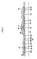
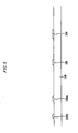
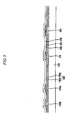
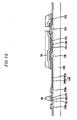
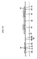
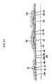
- FIG 1 is a plan view showing a pixel of a liquid crystal display according to one embodiment of this invention.
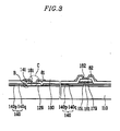
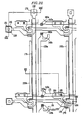
- FIG. 2 Is a cross-sectional view taken along line II-II' of FIG. 1 .
- FIG. 3 is a cross-sectional view taken along line III-III' of FIG. 1 .
- a plurality of gate lines 121 and storage electrode lines 131 are formed on a insulation substrate 110,
- Each gate line 121 extends in a row direction and provides a gate signal.
- the gate line 121 includes a gate electrode 124 and a gate pad 129,
- the gate electrode 124 is a portion formed in a pixel as a protrusion shape, and the gate pad 129 is a portion formed in a peripheral of the pixel to connect to other circuits.
- a gate drive circuit may be formed on a flexible printed circuit film or may be directly formed on the lower substrate 110.
- the gate line 121 receives a gate signal directly from the gate drive circuit.
- the storage line 131 runs parallel to the gate line 121 receives a certain level of voltage, and includes storage electrodes 133a, 133bextending from the storage line,
- the storage line 131 is formed between two consecutive gate lines 121.
- One end portion, a fixed portion, of the each storage electrode 133a and 133b is connected to the storage line 131, The other end portion is freely formed without connection,
- the first storage electrode 133a is narrower width-wise than the second storage electrode 133b.
- a shape and arrangement of the storage electrodes can be formed in various shapes.
- the gate line 121 and the storage electrode line 131 may be formed of aluminum (Al) or an aluminum alloy, silver (Ag) or a silver alloy, copper (Cu) or a copper alloy, molybdenum (Mo) or a molybdenum alloy, chrome (Cr), tantalum (Ta) or titanium (Ti).
- the gate line 121 can be formed by multi-layer structure having at least two different physical characteristics.
- one of the layers may be formed of low resistance material, such as aluminum, , silver or copper,
- the other layer is formed of another material such as molybdenum, chrome, titanium, or tantalum having excellent physical, chemical, electrical quality to contact with indium tin oxide (ITO) or indium zinc oxide (IZO).
- ITO indium tin oxide
- IZO indium zinc oxide
- One example of this combination is forming chrome as the lower metal layer, and aluminum alloy as the upper metal layer, or aluminum alloy as the lower metal layer and a molybdenum alloy as the upper metal.
- the gate line 121, the gate pad 124 and a storage line 131 can be formed using various metals and electric conductors.
- the lateral face of the gate line 121, the gate pad 124 and the storage line 131 is inclined to the lower substrate 110, and it is desirable that the tilt angle as measured from the adjacent surface at the substrate be about 30' or about 80'.
- a gate insulator 140 is formed of silicon nitride (SiNx) or silicon oxide (SiOx).
- This gate insulator 140 includes a lower film 140p and upper film 140q.
- the lower film 140p has a thickness of about 4,000 ⁇
- the upper gate film 140q has a thickness of about 500 ⁇ .
- the gate insulator 140 includes a plurality of contact holes 141,143a, and 143b, in which the contact hole 141 is for exposing the gate pad 129 of gate line 121, the contact hole 143a for exposing one part of a storage line 131, the contact hole 143b for exposing the end portion of the first storage electrode 133a.
- a semiconductor layer 151 is formed of poly-silicon.
- the poly-silicon semiconductor 151 generally extends in a column direction and includes a protrusion portion 154.
- Ohmic contact layers 161, 165 which are linear and island types are gradually formed over the semiconductor layer 151.
- the ohmic contact layers 161, 163 and 165 are made of amorphous silicon, which is doped by n-type phosphorus or p-type boron, polycrystalline silicon or silicide silicon.
- the ohmic contact layer 163 and 165 are formed over the protrusion portion 154 of the semiconductor layer 165.
- the lateral shape of semiconductor layers 151, 154 and ohmic contact layers 161, 163, 165 are inclined to the lower substrate 110 by about 30' or 80°.
- a drain electrode 175 and a data line 171 are formed.
- the data line 171 provides a data signal and traverses the gate line.
- Each data line 171 traverses the storage line 131 and is formed between the first storage electrode 133a in a current pixel and a storage electrode 133b in an adjacent pixel.
- the data line 171 includes a source electrode 173 and a data pad 179, In which the source electrode 173 extends to the gate electrode 124 and the data pad 179 is widen to connect with other circuitries,
- a data drive circuit which generates data signals is formed on a flexible printed circuit film attached on the lower substrate 110.
- the data driver circuit may be formed in the lower substrate 110 so as to directly connect to the data line 171.
- Drain electrode 175 is formed apart from the data line 171 and is faced to a source electrode 173 over the gate electrode 124.
- Each drain electrode 175 has a first end point which is a widen area type and a second end point which is a bar type. One part of the second end part is surrounded by the source electrode 173.
- a thin film transistor thin film transistor TFT is accomplished with a projecting part 154 of the semiconductor layer 151, and the channel of the thin film transistor is formed on the projecting part 154 positioned between the source electrode 173 and the drain electrode 175.
- the data line 171 and the drain electrode 175 are desirable to be formed of a refractory metal or Its alloy such as molybdenum, chrome, tantalum or titanium, and may have a multi-layer structure including a refractory metal and a low resistance conductive material,
- the multi-layer structure may be two layers or triple layers,
- the two layers are made of a lower film and an upper film, in which the lower film may be chrome (alloy) or molybdenum (alloy) and the upper film may be aluminum (alloy).
- the triple layers are made of triple films, for example molybdenum (alloy) as a lower film, aluminum (alloy) as an intermediate film and molybdenum (alloy) as an upper film.
- the data line 171 and the drain electrode 175, however, can be formed of various metal or electric conductors.
- Each side of the data conductors 171, 175 is desirable to have a tilt angle about 30' or 80' for the lower substrate 110.
- Ohmic contact layers 161, 165 exist over the semiconductor layer 151 and under the data line 171 and the drain electrode 175 to reduce contact resistance.
- the semiconductor layer 151 includes exposed portions which are not covered by the source electrode 173, the drain electrode 175 and the data line 171,
- a passivation layer 180 is formed.
- the width of the semiconductor layer 151 is wider than that of the data line 171 in a potion that the gate line 121 is formed so that a profile of the surface becomes smooth, the data line 171 is protected from disconnection,
- the passivation layer 180 is formed of inorganic insulating material, such as silicon nitride (SiNx) or silicon oxide (SiOx).
- the passivation layer 180 may be a combination of a lower passivation layer and upper passivation layer (not shown), in which the lower passivation layer is formed by organic insulating material or inorganic insulating material and also the upper passivation layer is formed by organic insulating material.
- the organic insulating material may be photosensitive material having a dielectric constant under 4.0.
- the passivation layer 180 also includes a contact hole 181 to expose a gate pad 129 of the gate line 121, a contact hole 182 to expose a data pad 170 of the data line 171, a contact hole 185 to expose a drain electrode, a contact hole 183a to expose one part of the storage line 131 near a storage electrode 183a and a contact hole 183b to expose a storage electrode 183b.
- a cross sectional area of the contact holes 181, 182, 183a, 183b and 185 becomes wide from bottom to top area, Namely, lateral sides of the contact holes 181, 182, 183a, 183b and 185 have a taper structure as shown in A of FIG. 2 and C of FIG. 3 .
- the contact hole 181 to expose the gate pad, a contact hole 183a to expose a fixed portion of the first storage electrode 133a, and a contact hole 183b to expose the free end of the first storage electrode 133a are formed in inner portion of the contact holes 141, 143a and 143b of gate insulator 140, respectively. Lateral sides of the contact holes 141, 143a and 143b have a taper structure.
- a plurality of pixel electrodes 191, a plurality of connecting legs 83 and a plurality of contact assistants 81, 82 are formed of transparent material such as ITO, IZO, or reflective metal such as aluminum (alloy), silver (alloy), or chrome (alloy).
- a taper structure of is applied to the contact holes 181, 182 and 185 in which a pixel electrode 191, connecting leg 83 and contact assistants 81, 82 are formed.
- the pixel electrode 191 is electrically and physically coupled to the drain electrode 175 via a contact hole 185, and also receives a data voltage from the drain electrode 175.
- Orientation of liquid crystal molecules is determined by the electric field which is applied between a pixel electrode 191 which receives a data voltage and a common electrode which receives a common voltage.
- the polarized light passing through the liquid crystal layer is varied.
- a liquid crystal capacitor formed between the pixel electrode 191 and common electrode maintains a supplied voltage even after a thin film transistor is turned off.
- the pixel electrode 191 is overlapped with the storage electrodes 133a, 133b and the storage line 131.
- a storage capacitor is formed between the pixel electrode 191 connected to the drain electrode 171 and the storage line 131, and also enforces the voltage holding ability of liquid crystal capacitor.
- Contact assistants 81, 82 are coupled to the gate pad 129 of the gate line 121, and the data pad 179 of the data line 171, respectively, via contact holes 181, 182, respectively, to permit contact with external devices,
- connection leg 83 crossing the gate line 121 the storage line 131 is linked to the free end of the first storage electrode 133a via contact holes 183a, 183b.
- the storage electrodes 133a, 133b and the storage line 131 may be used to fix a defect of the gate line 121, data line 171 or thin film transistor but also the storage line 131.
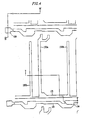
- a manufacturing method of a liquid crystal display device for FIG. 1 to FIG. 3 Is shown in FIG. 4 to FIG. 22 .
- FIG. 4 , F1G.17 and FIG. 20 are plane views useful for showing a manufacturing process of a liquid crystal display panel.
- FIG. 5 and FIG. 6 are cross-sectional views taken along line V-V', and VI-VI' of FIG, 4 ,
- FIG, 7 , FIG, 9 , FIG, 11 , FIG. 13 and FIG. 15 are cross-sectional views illustrating a forming process over a gate line and a storage line of FIG. 5 .
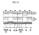
- FIG. 8 , 10 , 12 , 14 and 16 are cross-sectional views illustrating a forming process over a data line of FIG. 6 .
- FIG. 18 and FIG. 19 are cross-sectional views taken along line XVIII-XVIII', and XIX-XIX' of FIG. 17 .
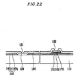
- FIG, 21 and FIG. 22 are a cross-sectional view taken along line XXI-XXI', and XXII-XXII' of FIG. 20 .
- a metal layer is deposited by sputtering process on the lower substrate 110 formed of glass or plastic, and then an etching process is applied to the metal layer in order to form a gate electrode 124, a gate pad 129, a gate line 121, a first storage electrode 133a, a second storage electrode 133b and a storage line 131.
- a gate insulator 140 is formed over the gate line 121, the storage line 131 and the lower substrate 110.
- the gate insulator 140 is made of silicon nitride or silicon oxide, and includes a lower gate insulator 140p and an upper gate insulator 140q which are sequentially formed over the lower substrate 110,
- the thickness of the lower gate Insulator 140p is about 4,000 ⁇ and the thickness of the upper gate insulator is about 500 ⁇ .
- a plasma enhanced chemical vapor deposition PECVD method is applied to form an intrinsic amorphous silicon a-Si layer 150, in which the intrinsic amorphous silicon a-Si layer 150 includes two layers, intrinsic amorphous silicon a-Si layer 150 and extrinsic amorphous silicon a-Si layer 160.
- the intrinsic amorphous silicon a-Si layer 150 is made of hydrogenated amorphous silicon
- the extrinsic amorphous silicon n+ a-Si layer 160 is made of amorphous silicon or silicide highly doped with n-type impurities such as phosphorus P.
- a data layer 170 is formed of molybdenum over the extrinsic amorphous silicon n+ a-Si layer 160.
- a photosensitive layer 50 is formed over the data layer 170, and then a photo mask 40 is arranged over the photosensitive layer 50,
- the photo mask 40 includes a light protection layer 42 on a transparent substrate 41, the light blocking layer being divided into a light blocking region BA, a full light transmission region TA, a half light transmission region HA and a slit region SA.
- the light protection layer 42 is formed in the light protection region BA to block all lights, and provides partial light transmission region HA.
- the light protection layer 42 is not formed in the light transmission region TA, thus there is full light transmission, and is formed with slits in region SA, the slits being arranged in the form of projections or columns having a certain width in the slit region SA.
- the light protection layer 42 of the half transmission region HA is thinner than the light protection region BA, and therefore the quantity of light passing the half light transmission region HA is less than the slit area SA, but more than in the light transmission region TA,
- the light protection layer 42 may be made of metal, such as chrome (Cr).
- Reference character 51 indicates the portion of the photosensitive film which is removed.
- the portions of the photosensitive film 50 beneath light protection regions BA are fully protected and remain full thickness, but the portion of photosensitive film beneath the light transmission region TA is fully developed and is removed.
- the photosensitive film 50 beneath the half transmission region HA is about 50% developed and accordingly 50% removed.
- the photosensitive film 50 beneath the slit region SA is developed to a lesser thickness than the half transmission region HA because of the difference in light exposure.
- the data layer 170 is etched using photo sensitive film 52 as a mask, and then the other layers, such as the extrinsic amorphous silicon 160, the intrinsic amorphous silicon layer 150 and the gate insulator film 140, are consecutively etched.
- the lower film 140p of the gate insulator 140 is not etched at the gate pad 129 of the gate line which has the thickness of about 500 ⁇ or 800 ⁇ .
- portions of photo sensitive film 52 have been removed, and the data layer 170 is revealed. More particularly, the portions of photo sensitive film 52 which were beneath the half light transmission region HA have been fully removed. However, the remaining portions of photo sensitive film 53 which were beneath the light protection region BA and slit region SA remain. This process results in the production of a second photosensitive film pattern.
- the process of removing portions of the photosensitive film to create the second photosensitive film pattern is known as ashing.
- the data layer 170, the extrinsic amorphous silicon layer 160 and the intrinsic amorphous silicon layer 150 are removed by etching so that a source-draln pattern 174, a data pad 179 of the data line 171 and a protrusion 154 of the semiconductor layer 151 are formed.
- the source-drain pattern 174 is a conductive pattern in which a source electrode is coupled to a drain electrode. A portion of part of the gate insulator 140 is removed, leaving lower film 140p of the gate insulator 140 over the gate pad 129 at the edge of the gate line 121 with a thickness of about less 200 ⁇ .
- the photo sensitive film 53 is ashed; the source drain pattern 174 is exposed.
- the photo sensitive film 53 which was beneath the slit region SA is fully removed and the regions of the photo sensitive film 54 indicated by reference character which were beneath the light protection regions BA remain.
- the photo sensitive film 54 has a thickness which is equal to the thickness of the photoresist removed in the area which was beneath slit region SA.
- a protrusion area 154 of the semiconductor layer 151 is exposed by sequentially etching the source-drain pattern 174 and the doped amorphous silicon pattern 164.
- a source electrode 173 and a drain electrode 175 are formed.
- the extrinsic amorphous silicon pattern 164 is achieved by an over etching process.
- the gate insulator 140 is removed by a certain amount of thickness, and includes a contact hole 141 which is formed by fully removing the lower film 140p of the gate Insulator 140 over the gate pad 129.
- The, the photo sensitive film 54 is removed.
- the passivation layer 180 is formed over the gate Insulator 140, a gate pad 129, a data line 171, and a drain electrode 175.
- the passivation layer 180 is generally formed of non-organic material such as silicon nitride SiNx or oxidation silicon SiOx.
- the passivation layer 180 includes an upper and lower passivation layer, in which the upper overcoating layer is formed of non-organic insulator and the lower passivation layer is formed of organic insulator.
- the organic insulator may be photosensitive and may have a dielectric constant preferably about 4.0 or less.
- contact holes 181, 182, 183a, 183b, 185 are formed, in which a contact hole 181 is for exposing a gate pad 129, a contact hole 182 for a data pad, a contact hole 183a for one end of the first storage electrode 133a, a contact hole 183b for the other end of the first storage electrode 133a and a contact hole 185 for a drain electrode 175.
- exposing time for etching is almost evenly applied to the gate pad 129, data pad 179 and storage electrodes 133a, 133b of the storage line 131 via contact holes 181, 182, 183a, 183b and 185,
- a transparent electrode ITO or IZO are deposited by sputtering process; a plurality of pixel electrodes 191, a connection leg 83 and contact members 81, 82 are formed using a photolithograph process by photo process.
Landscapes
- Physics & Mathematics (AREA)
- Nonlinear Science (AREA)
- Mathematical Physics (AREA)
- Chemical & Material Sciences (AREA)
- Crystallography & Structural Chemistry (AREA)
- General Physics & Mathematics (AREA)
- Optics & Photonics (AREA)
- Engineering & Computer Science (AREA)
- Microelectronics & Electronic Packaging (AREA)
- Liquid Crystal (AREA)
- Thin Film Transistor (AREA)
- Internal Circuitry In Semiconductor Integrated Circuit Devices (AREA)
Applications Claiming Priority (1)
| Application Number | Priority Date | Filing Date | Title |
|---|---|---|---|
| KR1020060085089A KR101282404B1 (ko) | 2006-09-05 | 2006-09-05 | 액정 표시 장치의 제조 방법 |
Publications (2)
| Publication Number | Publication Date |
|---|---|
| EP1898255A1 EP1898255A1 (en) | 2008-03-12 |
| EP1898255B1 true EP1898255B1 (en) | 2011-05-04 |
Family
ID=38611036
Family Applications (1)
| Application Number | Title | Priority Date | Filing Date |
|---|---|---|---|
| EP07017301A Active EP1898255B1 (en) | 2006-09-05 | 2007-09-04 | Method of manufacturing liquid crystal display |
Country Status (6)
| Country | Link |
|---|---|
| US (1) | US7868958B2 (enExample) |
| EP (1) | EP1898255B1 (enExample) |
| JP (1) | JP5229775B2 (enExample) |
| KR (1) | KR101282404B1 (enExample) |
| CN (1) | CN101221925B (enExample) |
| DE (1) | DE602007014301D1 (enExample) |
Families Citing this family (3)
| Publication number | Priority date | Publication date | Assignee | Title |
|---|---|---|---|---|
| KR101522615B1 (ko) * | 2008-11-05 | 2015-05-22 | 삼성디스플레이 주식회사 | 박막 트랜지스터 표시판 및 그 제조 방법 |
| JP6076038B2 (ja) * | 2011-11-11 | 2017-02-08 | 株式会社半導体エネルギー研究所 | 表示装置の作製方法 |
| KR102479019B1 (ko) | 2015-03-05 | 2022-12-19 | 삼성디스플레이 주식회사 | 플렉서블 표시장치 |
Family Cites Families (19)
| Publication number | Priority date | Publication date | Assignee | Title |
|---|---|---|---|---|
| JP3098345B2 (ja) * | 1992-12-28 | 2000-10-16 | 富士通株式会社 | 薄膜トランジスタマトリクス装置及びその製造方法 |
| JPH06250211A (ja) * | 1993-02-23 | 1994-09-09 | Hitachi Ltd | 液晶表示基板とその製造方法 |
| JP2001133804A (ja) | 1999-10-29 | 2001-05-18 | Fujitsu Ltd | 液晶表示装置の製造方法 |
| KR100476366B1 (ko) * | 2002-04-17 | 2005-03-16 | 엘지.필립스 엘시디 주식회사 | 박막 트랜지스터 어레이 기판 및 그 제조 방법 |
| JP4565799B2 (ja) | 2002-07-01 | 2010-10-20 | 大林精工株式会社 | 横電界方式液晶表示装置、その製造方法、走査露光装置およびミックス走査露光装置 |
| JP2004212933A (ja) | 2002-12-31 | 2004-07-29 | Lg Phillips Lcd Co Ltd | 液晶表示装置及びアレイ基板の製造方法 |
| KR100598737B1 (ko) | 2003-05-06 | 2006-07-10 | 엘지.필립스 엘시디 주식회사 | 박막 트랜지스터 어레이 기판 및 그 제조 방법 |
| KR100499376B1 (ko) * | 2003-10-10 | 2005-07-04 | 엘지.필립스 엘시디 주식회사 | 박막 트랜지스터 어레이 기판 및 그 제조 방법 |
| TWI234043B (en) * | 2003-11-26 | 2005-06-11 | Hannstar Display Corp | Method of manufacturing liquid crystal display |
| KR101050292B1 (ko) * | 2003-12-27 | 2011-07-19 | 엘지디스플레이 주식회사 | 박막트랜지스터 어레이 기판의 제조방법 |
| KR101003577B1 (ko) * | 2003-12-29 | 2010-12-23 | 엘지디스플레이 주식회사 | 마스크 및 이를 이용한 액정표시소자 제조방법 |
| KR100675634B1 (ko) | 2003-12-30 | 2007-02-01 | 엘지.필립스 엘시디 주식회사 | 액정표시소자의 제조방법 |
| KR20050105422A (ko) | 2004-05-01 | 2005-11-04 | 엘지.필립스 엘시디 주식회사 | 액정표시패널 및 그 제조 방법 |
| KR101126396B1 (ko) | 2004-06-25 | 2012-03-28 | 엘지디스플레이 주식회사 | 박막트랜지스터 어레이 기판 및 그 제조방법 |
| KR101061844B1 (ko) | 2004-06-29 | 2011-09-02 | 삼성전자주식회사 | 박막 표시판의 제조 방법 |
| KR20060023716A (ko) | 2004-09-10 | 2006-03-15 | 삼성전자주식회사 | 반사-투과형 액정표시장치의 제조방법 |
| KR100640620B1 (ko) * | 2004-12-27 | 2006-11-02 | 삼성전자주식회사 | 트윈비트 셀 구조의 nor형 플래쉬 메모리 소자 및 그제조 방법 |
| TWI368327B (en) * | 2005-01-17 | 2012-07-11 | Samsung Electronics Co Ltd | Optical mask and manufacturing method of thin film transistor array panel using the optical mask |
| JP4301259B2 (ja) * | 2005-09-13 | 2009-07-22 | エプソンイメージングデバイス株式会社 | 液晶表示装置及びその製造方法 |
-
2006
- 2006-09-05 KR KR1020060085089A patent/KR101282404B1/ko active Active
-
2007
- 2007-08-30 JP JP2007224357A patent/JP5229775B2/ja active Active
- 2007-08-31 US US11/897,769 patent/US7868958B2/en active Active
- 2007-09-04 EP EP07017301A patent/EP1898255B1/en active Active
- 2007-09-04 DE DE602007014301T patent/DE602007014301D1/de active Active
- 2007-09-05 CN CN2007103069009A patent/CN101221925B/zh active Active
Also Published As
| Publication number | Publication date |
|---|---|
| JP5229775B2 (ja) | 2013-07-03 |
| EP1898255A1 (en) | 2008-03-12 |
| US20080106685A1 (en) | 2008-05-08 |
| US7868958B2 (en) | 2011-01-11 |
| JP2008066723A (ja) | 2008-03-21 |
| CN101221925B (zh) | 2011-06-29 |
| CN101221925A (zh) | 2008-07-16 |
| DE602007014301D1 (de) | 2011-06-16 |
| KR20080021909A (ko) | 2008-03-10 |
| KR101282404B1 (ko) | 2013-07-04 |
Similar Documents
| Publication | Publication Date | Title |
|---|---|---|
| KR101373735B1 (ko) | 신호선의 제조 방법, 박막 트랜지스터 표시판 및 그의 제조방법 | |
| KR20090096226A (ko) | 박막 트랜지스터 표시판 및 그 제조 방법 | |
| JP2006049889A (ja) | 薄膜トランジスタ表示板及びその製造方法 | |
| US7932965B2 (en) | Thin film transistor array panel and method for manufacturing the same | |
| US7422916B2 (en) | Method of manufacturing thin film transistor panel | |
| EP1898255B1 (en) | Method of manufacturing liquid crystal display | |
| KR101171187B1 (ko) | 박막 트랜지스터 표시판, 그 제조 방법 및 이를 포함하는액정 표시 장치 | |
| US7462895B2 (en) | Signal line for display device and thin film transistor array panel including the signal line | |
| KR101160823B1 (ko) | 박막 트랜지스터 표시판과 그 제조 방법 | |
| US7541225B2 (en) | Method of manufacturing a thin film transistor array panel that includes using chemical mechanical polishing of a conductive film to form a pixel electrode connected to a drain electrode | |
| KR101209045B1 (ko) | 박막 트랜지스터 표시판 및 그 제조 방법 | |
| KR101184640B1 (ko) | 박막 트랜지스터 표시판 및 그 제조 방법 | |
| JP2007142388A (ja) | 薄膜トランジスタ表示板及びその製造方法 | |
| US10128274B2 (en) | Thin film transistor array panel and a method for manufacturing the same | |
| KR100997969B1 (ko) | 박막 트랜지스터 표시판 및 그의 제조 방법 | |
| KR20070014336A (ko) | 박막 트랜지스터 표시판 및 그 제조 방법 | |
| KR20080027582A (ko) | 박막 트랜지스터 표시판 및 그 제조 방법 | |
| KR20080014239A (ko) | 액정 표시 장치의 제조 방법 | |
| KR20080053645A (ko) | 박막 트랜지스터 표시판 및 그 제조 방법 | |
| KR20070014335A (ko) | 박막 트랜지스터 표시판의 제조 방법 | |
| KR20050093881A (ko) | 박막 트랜지스터 표시판의 제조 방법 | |
| KR20080049985A (ko) | 액정 표시 장치 및 그 제조 방법 | |
| KR20060058404A (ko) | 박막 트랜지스터 표시판의 제조 방법 | |
| KR20080011748A (ko) | 액정 표시 장치의 제조 방법 | |
| KR20070039758A (ko) | 박막 트랜지스터 표시판의 제조 방법 |
Legal Events
| Date | Code | Title | Description |
|---|---|---|---|
| PUAI | Public reference made under article 153(3) epc to a published international application that has entered the european phase |
Free format text: ORIGINAL CODE: 0009012 |
|
| AK | Designated contracting states |
Kind code of ref document: A1 Designated state(s): AT BE BG CH CY CZ DE DK EE ES FI FR GB GR HU IE IS IT LI LT LU LV MC MT NL PL PT RO SE SI SK TR |
|
| AX | Request for extension of the european patent |
Extension state: AL BA HR MK YU |
|
| 17P | Request for examination filed |
Effective date: 20080912 |
|
| 17Q | First examination report despatched |
Effective date: 20081014 |
|
| AKX | Designation fees paid |
Designated state(s): DE FR GB |
|
| GRAP | Despatch of communication of intention to grant a patent |
Free format text: ORIGINAL CODE: EPIDOSNIGR1 |
|
| GRAS | Grant fee paid |
Free format text: ORIGINAL CODE: EPIDOSNIGR3 |
|
| GRAA | (expected) grant |
Free format text: ORIGINAL CODE: 0009210 |
|
| AK | Designated contracting states |
Kind code of ref document: B1 Designated state(s): DE FR GB |
|
| REG | Reference to a national code |
Ref country code: GB Ref legal event code: FG4D |
|
| REF | Corresponds to: |
Ref document number: 602007014301 Country of ref document: DE Date of ref document: 20110616 Kind code of ref document: P |
|
| REG | Reference to a national code |
Ref country code: DE Ref legal event code: R096 Ref document number: 602007014301 Country of ref document: DE Effective date: 20110616 |
|
| PLBE | No opposition filed within time limit |
Free format text: ORIGINAL CODE: 0009261 |
|
| STAA | Information on the status of an ep patent application or granted ep patent |
Free format text: STATUS: NO OPPOSITION FILED WITHIN TIME LIMIT |
|
| 26N | No opposition filed |
Effective date: 20120207 |
|
| REG | Reference to a national code |
Ref country code: DE Ref legal event code: R097 Ref document number: 602007014301 Country of ref document: DE Effective date: 20120207 |
|
| REG | Reference to a national code |
Ref country code: FR Ref legal event code: TP Owner name: SAMSUNG DISPLAY CO. LTD, KR Effective date: 20130226 |
|
| REG | Reference to a national code |
Ref country code: GB Ref legal event code: 732E Free format text: REGISTERED BETWEEN 20130307 AND 20130313 |
|
| REG | Reference to a national code |
Ref country code: DE Ref legal event code: R082 Ref document number: 602007014301 Country of ref document: DE Representative=s name: DR. WEITZEL & PARTNER, DE |
|
| REG | Reference to a national code |
Ref country code: DE Ref legal event code: R082 Ref document number: 602007014301 Country of ref document: DE Representative=s name: DR. WEITZEL & PARTNER, DE Effective date: 20130422 Ref country code: DE Ref legal event code: R081 Ref document number: 602007014301 Country of ref document: DE Owner name: SAMSUNG DISPLAY CO., LTD., KR Free format text: FORMER OWNER: SAMSUNG ELECTRONICS CO., LTD., SUWON-SI, KR Effective date: 20130422 Ref country code: DE Ref legal event code: R082 Ref document number: 602007014301 Country of ref document: DE Representative=s name: DR. WEITZEL & PARTNER PATENT- UND RECHTSANWAEL, DE Effective date: 20130422 Ref country code: DE Ref legal event code: R081 Ref document number: 602007014301 Country of ref document: DE Owner name: SAMSUNG DISPLAY CO., LTD., YONGIN-CITY, KR Free format text: FORMER OWNER: SAMSUNG ELECTRONICS CO., LTD., SUWON-SI, GYEONGGI-DO, KR Effective date: 20130422 |
|
| REG | Reference to a national code |
Ref country code: FR Ref legal event code: PLFP Year of fee payment: 10 |
|
| REG | Reference to a national code |
Ref country code: FR Ref legal event code: PLFP Year of fee payment: 11 |
|
| REG | Reference to a national code |
Ref country code: FR Ref legal event code: PLFP Year of fee payment: 12 |
|
| P01 | Opt-out of the competence of the unified patent court (upc) registered |
Effective date: 20230515 |
|
| PGFP | Annual fee paid to national office [announced via postgrant information from national office to epo] |
Ref country code: DE Payment date: 20250820 Year of fee payment: 19 |
|
| PGFP | Annual fee paid to national office [announced via postgrant information from national office to epo] |
Ref country code: GB Payment date: 20250820 Year of fee payment: 19 |
|
| PGFP | Annual fee paid to national office [announced via postgrant information from national office to epo] |
Ref country code: FR Payment date: 20250821 Year of fee payment: 19 |