EP1850430A2 - Halbleiterlaserbauelement und Verfahren zu seiner Herstellung - Google Patents
Halbleiterlaserbauelement und Verfahren zu seiner Herstellung Download PDFInfo
- Publication number
- EP1850430A2 EP1850430A2 EP07003455A EP07003455A EP1850430A2 EP 1850430 A2 EP1850430 A2 EP 1850430A2 EP 07003455 A EP07003455 A EP 07003455A EP 07003455 A EP07003455 A EP 07003455A EP 1850430 A2 EP1850430 A2 EP 1850430A2
- Authority
- EP
- European Patent Office
- Prior art keywords
- diffraction grating
- layer
- semiconductor laser
- laser device
- etching
- Prior art date
- Legal status (The legal status is an assumption and is not a legal conclusion. Google has not performed a legal analysis and makes no representation as to the accuracy of the status listed.)
- Granted
Links
Images
Classifications
-
- H—ELECTRICITY
- H01—ELECTRIC ELEMENTS
- H01S—DEVICES USING THE PROCESS OF LIGHT AMPLIFICATION BY STIMULATED EMISSION OF RADIATION [LASER] TO AMPLIFY OR GENERATE LIGHT; DEVICES USING STIMULATED EMISSION OF ELECTROMAGNETIC RADIATION IN WAVE RANGES OTHER THAN OPTICAL
- H01S5/00—Semiconductor lasers
- H01S5/10—Construction or shape of the optical resonator, e.g. extended or external cavity, coupled cavities, bent-guide, varying width, thickness or composition of the active region
- H01S5/12—Construction or shape of the optical resonator, e.g. extended or external cavity, coupled cavities, bent-guide, varying width, thickness or composition of the active region the resonator having a periodic structure, e.g. in distributed feedback [DFB] lasers
-
- B—PERFORMING OPERATIONS; TRANSPORTING
- B82—NANOTECHNOLOGY
- B82Y—SPECIFIC USES OR APPLICATIONS OF NANOSTRUCTURES; MEASUREMENT OR ANALYSIS OF NANOSTRUCTURES; MANUFACTURE OR TREATMENT OF NANOSTRUCTURES
- B82Y20/00—Nanooptics, e.g. quantum optics or photonic crystals
-
- H—ELECTRICITY
- H01—ELECTRIC ELEMENTS
- H01S—DEVICES USING THE PROCESS OF LIGHT AMPLIFICATION BY STIMULATED EMISSION OF RADIATION [LASER] TO AMPLIFY OR GENERATE LIGHT; DEVICES USING STIMULATED EMISSION OF ELECTROMAGNETIC RADIATION IN WAVE RANGES OTHER THAN OPTICAL
- H01S5/00—Semiconductor lasers
- H01S5/10—Construction or shape of the optical resonator, e.g. extended or external cavity, coupled cavities, bent-guide, varying width, thickness or composition of the active region
- H01S5/12—Construction or shape of the optical resonator, e.g. extended or external cavity, coupled cavities, bent-guide, varying width, thickness or composition of the active region the resonator having a periodic structure, e.g. in distributed feedback [DFB] lasers
- H01S5/1231—Grating growth or overgrowth details
-
- H—ELECTRICITY
- H01—ELECTRIC ELEMENTS
- H01S—DEVICES USING THE PROCESS OF LIGHT AMPLIFICATION BY STIMULATED EMISSION OF RADIATION [LASER] TO AMPLIFY OR GENERATE LIGHT; DEVICES USING STIMULATED EMISSION OF ELECTROMAGNETIC RADIATION IN WAVE RANGES OTHER THAN OPTICAL
- H01S5/00—Semiconductor lasers
- H01S5/10—Construction or shape of the optical resonator, e.g. extended or external cavity, coupled cavities, bent-guide, varying width, thickness or composition of the active region
- H01S5/12—Construction or shape of the optical resonator, e.g. extended or external cavity, coupled cavities, bent-guide, varying width, thickness or composition of the active region the resonator having a periodic structure, e.g. in distributed feedback [DFB] lasers
- H01S5/125—Distributed Bragg reflector [DBR] lasers
-
- H—ELECTRICITY
- H01—ELECTRIC ELEMENTS
- H01S—DEVICES USING THE PROCESS OF LIGHT AMPLIFICATION BY STIMULATED EMISSION OF RADIATION [LASER] TO AMPLIFY OR GENERATE LIGHT; DEVICES USING STIMULATED EMISSION OF ELECTROMAGNETIC RADIATION IN WAVE RANGES OTHER THAN OPTICAL
- H01S5/00—Semiconductor lasers
- H01S5/30—Structure or shape of the active region; Materials used for the active region
- H01S5/34—Structure or shape of the active region; Materials used for the active region comprising quantum well or superlattice structures, e.g. single quantum well [SQW] lasers, multiple quantum well [MQW] lasers or graded index separate confinement heterostructure [GRINSCH] lasers
- H01S5/343—Structure or shape of the active region; Materials used for the active region comprising quantum well or superlattice structures, e.g. single quantum well [SQW] lasers, multiple quantum well [MQW] lasers or graded index separate confinement heterostructure [GRINSCH] lasers in AIIIBV compounds, e.g. AlGaAs-laser, InP-based laser
- H01S5/34306—Structure or shape of the active region; Materials used for the active region comprising quantum well or superlattice structures, e.g. single quantum well [SQW] lasers, multiple quantum well [MQW] lasers or graded index separate confinement heterostructure [GRINSCH] lasers in AIIIBV compounds, e.g. AlGaAs-laser, InP-based laser emitting light at a wavelength longer than 1000nm, e.g. InP based 1300 and 1500nm lasers
-
- H—ELECTRICITY
- H01—ELECTRIC ELEMENTS
- H01S—DEVICES USING THE PROCESS OF LIGHT AMPLIFICATION BY STIMULATED EMISSION OF RADIATION [LASER] TO AMPLIFY OR GENERATE LIGHT; DEVICES USING STIMULATED EMISSION OF ELECTROMAGNETIC RADIATION IN WAVE RANGES OTHER THAN OPTICAL
- H01S5/00—Semiconductor lasers
- H01S5/30—Structure or shape of the active region; Materials used for the active region
- H01S5/34—Structure or shape of the active region; Materials used for the active region comprising quantum well or superlattice structures, e.g. single quantum well [SQW] lasers, multiple quantum well [MQW] lasers or graded index separate confinement heterostructure [GRINSCH] lasers
- H01S5/343—Structure or shape of the active region; Materials used for the active region comprising quantum well or superlattice structures, e.g. single quantum well [SQW] lasers, multiple quantum well [MQW] lasers or graded index separate confinement heterostructure [GRINSCH] lasers in AIIIBV compounds, e.g. AlGaAs-laser, InP-based laser
- H01S5/34313—Structure or shape of the active region; Materials used for the active region comprising quantum well or superlattice structures, e.g. single quantum well [SQW] lasers, multiple quantum well [MQW] lasers or graded index separate confinement heterostructure [GRINSCH] lasers in AIIIBV compounds, e.g. AlGaAs-laser, InP-based laser with a well layer having only As as V-compound, e.g. AlGaAs, InGaAs
Definitions
- a distributed feedback (DFB) laser using a refractive-index-modulation diffraction grating which has narrow spectrum and allows single mode oscillation
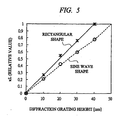
- a DFB laser light output and modulation characteristic significantly change according to ⁇ L, product of a coupling coefficient ⁇ of light diffracted in a waveguide direction and an oscillator length L. Therefore, in designing and manufacturing laser devices, it is important to set ⁇ L at a desired value.
- the coupling coefficient ⁇ is determined by height of the diffraction grating, distance from an active layer, and difference in refractive index between a diffraction grating layer and a buried layer (clad layer).
- the coupling coefficient ⁇ largely depends on the height of the diffraction grating.
- a primary component in a result of Fourier transform of a cross-section shape of the diffraction grating in the waveguide direction considered as a periodic waveform affects the magnitude of KL. Therefore, such a phenomenon as depicted in the drawing occurs. According to this result, by forming the diffraction grating in a sine wave shape, KL can be reduced by 21.5% ( ⁇ /4) compared with the case of a rectangular shape.
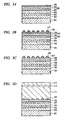
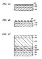
- a diffraction grating is formed through dry etching or wet etching. In this case, a shape of the diffraction grating become rectangular, and it is difficult to form a sine wave shape through etching.
- This sine wave shape can be formed through thermal decomposition at increase of temperature in burying regrowth. In this case, however, the above-mentioned problem occurs due to mass transport.
- An object of the present invention is to overcome the above-described problems, and to provide a semiconductor laser device manufacturing technology capable of reducing ⁇ L with manufacturing restrictions satisfied.
Landscapes
- Physics & Mathematics (AREA)
- Nanotechnology (AREA)
- Engineering & Computer Science (AREA)
- Chemical & Material Sciences (AREA)
- Optics & Photonics (AREA)
- Biophysics (AREA)
- Life Sciences & Earth Sciences (AREA)
- Electromagnetism (AREA)
- General Physics & Mathematics (AREA)
- Crystallography & Structural Chemistry (AREA)
- Condensed Matter Physics & Semiconductors (AREA)
- Semiconductor Lasers (AREA)
- Drying Of Semiconductors (AREA)
Applications Claiming Priority (1)
| Application Number | Priority Date | Filing Date | Title |
|---|---|---|---|
| JP2006122777A JP4951267B2 (ja) | 2006-04-27 | 2006-04-27 | 半導体レーザ素子の製造方法 |
Publications (3)
| Publication Number | Publication Date |
|---|---|
| EP1850430A2 true EP1850430A2 (de) | 2007-10-31 |
| EP1850430A3 EP1850430A3 (de) | 2009-12-16 |
| EP1850430B1 EP1850430B1 (de) | 2013-05-01 |
Family
ID=38442608
Family Applications (1)
| Application Number | Title | Priority Date | Filing Date |
|---|---|---|---|
| EP07003455.8A Active EP1850430B1 (de) | 2006-04-27 | 2007-02-19 | Verfahren zur Herstellung eines Halbleiterlaserelements |
Country Status (3)
| Country | Link |
|---|---|
| US (2) | US20080013582A1 (de) |
| EP (1) | EP1850430B1 (de) |
| JP (1) | JP4951267B2 (de) |
Cited By (1)
| Publication number | Priority date | Publication date | Assignee | Title |
|---|---|---|---|---|
| CN106785905A (zh) * | 2017-01-19 | 2017-05-31 | 桂林电子科技大学 | 一种基于布拉格相移光栅的电光调制器 |
Families Citing this family (5)
| Publication number | Priority date | Publication date | Assignee | Title |
|---|---|---|---|---|
| KR100958719B1 (ko) * | 2007-12-12 | 2010-05-18 | 한국전자통신연구원 | 단일모드 발진을 위한 하이브리드 레이저 다이오드 및 그제조 방법 |
| DE102008054217A1 (de) * | 2008-10-31 | 2010-05-06 | Osram Opto Semiconductors Gmbh | Optoelektronischer Halbleiterchip und Verfahren zur Herstellung eines optoelektronischen Halbleiterchips |
| JP5206976B2 (ja) * | 2009-03-06 | 2013-06-12 | 富士通株式会社 | 半導体レーザ及びその製造方法 |
| CN104201566B (zh) * | 2014-08-22 | 2017-12-29 | 华中科技大学 | 一种具有高单纵模成品率的脊波导分布反馈半导体激光器 |
| US11133649B2 (en) * | 2019-06-21 | 2021-09-28 | Palo Alto Research Center Incorporated | Index and gain coupled distributed feedback laser |
Citations (2)
| Publication number | Priority date | Publication date | Assignee | Title |
|---|---|---|---|---|
| JPS62150794A (ja) | 1985-12-24 | 1987-07-04 | Sony Corp | 分布帰還型半導体レ−ザ− |
| JPH098396A (ja) | 1995-06-19 | 1997-01-10 | Nec Corp | 分布帰還型半導体レーザ素子 |
Family Cites Families (15)
| Publication number | Priority date | Publication date | Assignee | Title |
|---|---|---|---|---|
| JPS63265485A (ja) * | 1987-04-23 | 1988-11-01 | Sony Corp | 半導体レ−ザ |
| JPS6454790A (en) * | 1987-08-26 | 1989-03-02 | Matsushita Electric Industrial Co Ltd | Distributed feedback type semiconductor laser |
| JP3204474B2 (ja) * | 1993-03-01 | 2001-09-04 | キヤノン株式会社 | 利得結合分布帰還型半導体レーザとその作製方法 |
| JP3374878B2 (ja) * | 1994-09-02 | 2003-02-10 | 三菱電機株式会社 | 半導体エッチング方法 |
| JP3751052B2 (ja) * | 1994-12-28 | 2006-03-01 | シャープ株式会社 | 集積型光制御素子およびその作製方法、並びにそれを備えた光集積回路素子および光集積回路装置 |
| US5633193A (en) * | 1996-05-22 | 1997-05-27 | Lucent Technologies Inc. | Method of making an InP-based device comprising semiconductor growth on a non-planar surface |
| JP3643486B2 (ja) * | 1998-08-04 | 2005-04-27 | 株式会社東芝 | 光機能素子及び光通信システム |
| EP1043818B1 (de) * | 1999-04-09 | 2011-07-20 | Mitsui Chemicals, Inc. | Halbleiterlaservorrichtung, seltenen erden dotierten Faserverstärker und Faserlaser |
| KR100632308B1 (ko) * | 2000-03-13 | 2006-10-11 | 샤프 가부시키가이샤 | 이득결합 분포귀환형 반도체레이저장치 및 그의 제조방법 |
| JP2001266389A (ja) * | 2000-03-23 | 2001-09-28 | Tdk Corp | 近接場光を用いる光ヘッド |
| JP4031263B2 (ja) * | 2002-03-05 | 2008-01-09 | 三菱電機株式会社 | 半導体レーザ装置の製造方法 |
| US6608855B1 (en) * | 2002-05-31 | 2003-08-19 | Applied Optoelectronics, Inc. | Single-mode DBR laser with improved phase-shift section |
| JP2005129833A (ja) * | 2003-10-27 | 2005-05-19 | Nec Kansai Ltd | 半導体レーザの製造方法 |
| JP4164438B2 (ja) * | 2003-11-12 | 2008-10-15 | 株式会社日立製作所 | 半導体光素子の製造方法 |
| JP2006108278A (ja) * | 2004-10-04 | 2006-04-20 | Matsushita Electric Ind Co Ltd | 半導体レーザ装置 |
-
2006
- 2006-04-27 JP JP2006122777A patent/JP4951267B2/ja active Active
-
2007
- 2007-02-19 EP EP07003455.8A patent/EP1850430B1/de active Active
- 2007-02-20 US US11/708,135 patent/US20080013582A1/en not_active Abandoned
-
2009
- 2009-10-02 US US12/572,720 patent/US7855093B2/en active Active
Patent Citations (2)
| Publication number | Priority date | Publication date | Assignee | Title |
|---|---|---|---|---|
| JPS62150794A (ja) | 1985-12-24 | 1987-07-04 | Sony Corp | 分布帰還型半導体レ−ザ− |
| JPH098396A (ja) | 1995-06-19 | 1997-01-10 | Nec Corp | 分布帰還型半導体レーザ素子 |
Cited By (1)
| Publication number | Priority date | Publication date | Assignee | Title |
|---|---|---|---|---|
| CN106785905A (zh) * | 2017-01-19 | 2017-05-31 | 桂林电子科技大学 | 一种基于布拉格相移光栅的电光调制器 |
Also Published As
| Publication number | Publication date |
|---|---|
| US7855093B2 (en) | 2010-12-21 |
| EP1850430B1 (de) | 2013-05-01 |
| US20080013582A1 (en) | 2008-01-17 |
| US20100022043A1 (en) | 2010-01-28 |
| JP2007294774A (ja) | 2007-11-08 |
| JP4951267B2 (ja) | 2012-06-13 |
| EP1850430A3 (de) | 2009-12-16 |
Similar Documents
| Publication | Publication Date | Title |
|---|---|---|
| US6292503B1 (en) | Ridge type semiconductor laser of laterally-coupled distributed feedback and method of manufacturing the same | |
| US5982804A (en) | Non-regrowth distributed feedback ridge semiconductor laser and method of manufacturing the same | |
| Nunoya et al. | High-performance 1.55-/spl mu/m wavelength GaInAsP-InP distributed-feedback lasers with wirelike active regions | |
| US8705583B2 (en) | Semiconductor laser | |
| US8494320B2 (en) | Optical element and method for manufacturing the same | |
| US7855093B2 (en) | Semiconductor laser device and method of manufacturing the same | |
| JP3842976B2 (ja) | 分布帰還型半導体レーザとその製造方法 | |
| JP5280614B2 (ja) | 単一のステップmocvdによって製造される導波格子を組み込んだ埋め込みヘテロ構造デバイス | |
| US7957446B2 (en) | Semiconductor laser and method of making semiconductor laser | |
| US8637338B2 (en) | Method for producing integrated optical device | |
| JP3204474B2 (ja) | 利得結合分布帰還型半導体レーザとその作製方法 | |
| JP3450169B2 (ja) | 分布帰還型半導体レーザ | |
| US20010036213A1 (en) | Ridge type semiconductor laser of distributed feedback | |
| JP5217767B2 (ja) | 半導体レーザ及び半導体レーザの製造方法 | |
| JP4151043B2 (ja) | 光半導体装置の製造方法 | |
| WO2007072807A1 (ja) | 半導体素子、および半導体素子の製造方法 | |
| JP2007184491A (ja) | 分布帰還型半導体レーザ | |
| US8846425B2 (en) | Diode laser and method for manufacturing a high-efficiency diode laser | |
| JP2002057405A (ja) | 半導体レーザ装置及びその製造方法 | |
| JP4992451B2 (ja) | 半導体レーザ、および半導体レーザを作製する方法 | |
| JP3455404B2 (ja) | 半導体光素子とその作製方法 | |
| JPH0642583B2 (ja) | 半導体レーザ装置 | |
| JP2783163B2 (ja) | 分布帰還型半導体レーザおよびその製造方法 | |
| JP2001168455A (ja) | 光半導体装置の製造方法 | |
| JP2810518B2 (ja) | 半導体レーザ装置およびその製造方法 |
Legal Events
| Date | Code | Title | Description |
|---|---|---|---|
| PUAI | Public reference made under article 153(3) epc to a published international application that has entered the european phase |
Free format text: ORIGINAL CODE: 0009012 |
|
| AK | Designated contracting states |
Kind code of ref document: A2 Designated state(s): AT BE BG CH CY CZ DE DK EE ES FI FR GB GR HU IE IS IT LI LT LU LV MC NL PL PT RO SE SI SK TR |
|
| AX | Request for extension of the european patent |
Extension state: AL BA HR MK YU |
|
| PUAL | Search report despatched |
Free format text: ORIGINAL CODE: 0009013 |
|
| AK | Designated contracting states |
Kind code of ref document: A3 Designated state(s): AT BE BG CH CY CZ DE DK EE ES FI FR GB GR HU IE IS IT LI LT LU LV MC NL PL PT RO SE SI SK TR |
|
| AX | Request for extension of the european patent |
Extension state: AL BA HR MK RS |
|
| 17P | Request for examination filed |
Effective date: 20100107 |
|
| 17Q | First examination report despatched |
Effective date: 20100209 |
|
| AKX | Designation fees paid |
Designated state(s): DE FR GB |
|
| GRAP | Despatch of communication of intention to grant a patent |
Free format text: ORIGINAL CODE: EPIDOSNIGR1 |
|
| GRAC | Information related to communication of intention to grant a patent modified |
Free format text: ORIGINAL CODE: EPIDOSCIGR1 |
|
| RAP1 | Party data changed (applicant data changed or rights of an application transferred) |
Owner name: OCLARO JAPAN, INC. |
|
| GRAP | Despatch of communication of intention to grant a patent |
Free format text: ORIGINAL CODE: EPIDOSNIGR1 |
|
| RIN1 | Information on inventor provided before grant (corrected) |
Inventor name: WASHINO, RYU C/O OCLARO JAPAN, INC. Inventor name: KOMATSU, KAZUHIRO C/O OCLARO JAPAN, INC. Inventor name: OKAMOTO, KAORU C/O OCLARO JAPAN, INC. Inventor name: SAKUMA, YASUSHI C/O OCLARO JAPAN, INC. |
|
| RIN1 | Information on inventor provided before grant (corrected) |
Inventor name: WASHINO, RYU Inventor name: SAKUMA, YASUSHI Inventor name: KOMATSU, KAZUHIRO Inventor name: OKAMOTO, KAORU |
|
| GRAS | Grant fee paid |
Free format text: ORIGINAL CODE: EPIDOSNIGR3 |
|
| GRAA | (expected) grant |
Free format text: ORIGINAL CODE: 0009210 |
|
| AK | Designated contracting states |
Kind code of ref document: B1 Designated state(s): DE FR GB |
|
| REG | Reference to a national code |
Ref country code: GB Ref legal event code: FG4D |
|
| REG | Reference to a national code |
Ref country code: DE Ref legal event code: R096 Ref document number: 602007030109 Country of ref document: DE Effective date: 20130627 |
|
| PLBE | No opposition filed within time limit |
Free format text: ORIGINAL CODE: 0009261 |
|
| STAA | Information on the status of an ep patent application or granted ep patent |
Free format text: STATUS: NO OPPOSITION FILED WITHIN TIME LIMIT |
|
| 26N | No opposition filed |
Effective date: 20140204 |
|
| REG | Reference to a national code |
Ref country code: DE Ref legal event code: R097 Ref document number: 602007030109 Country of ref document: DE Effective date: 20140204 |
|
| REG | Reference to a national code |
Ref country code: DE Ref legal event code: R082 Ref document number: 602007030109 Country of ref document: DE Representative=s name: BEETZ & PARTNER MBB, DE |
|
| REG | Reference to a national code |
Ref country code: FR Ref legal event code: CA Effective date: 20150424 |
|
| REG | Reference to a national code |
Ref country code: DE Ref legal event code: R082 Ref document number: 602007030109 Country of ref document: DE Representative=s name: BEETZ & PARTNER MBB, DE Effective date: 20150427 Ref country code: DE Ref legal event code: R081 Ref document number: 602007030109 Country of ref document: DE Owner name: OCLARO JAPAN, INC., SAGAMIHARA, JP Free format text: FORMER OWNER: OCLARO JAPAN, INC., YOKOHAMA-SHI, KANAGAWA, JP Effective date: 20150427 Ref country code: DE Ref legal event code: R081 Ref document number: 602007030109 Country of ref document: DE Owner name: OCLARO JAPAN, INC., SAGAMIHARA, JP Free format text: FORMER OWNER: OPNEXT JAPAN, INC., YOKOHAMA, KANAGAWA, JP Effective date: 20130503 Ref country code: DE Ref legal event code: R082 Ref document number: 602007030109 Country of ref document: DE Representative=s name: BEETZ & PARTNER MBB PATENTANWAELTE, DE Effective date: 20150427 Ref country code: DE Ref legal event code: R082 Ref document number: 602007030109 Country of ref document: DE Representative=s name: BEETZ & PARTNER MBB PATENT- UND RECHTSANWAELTE, DE Effective date: 20150427 |
|
| REG | Reference to a national code |
Ref country code: FR Ref legal event code: PLFP Year of fee payment: 10 |
|
| REG | Reference to a national code |
Ref country code: FR Ref legal event code: PLFP Year of fee payment: 11 |
|
| REG | Reference to a national code |
Ref country code: FR Ref legal event code: PLFP Year of fee payment: 12 |
|
| REG | Reference to a national code |
Ref country code: DE Ref legal event code: R082 Ref document number: 602007030109 Country of ref document: DE Representative=s name: BEETZ & PARTNER MBB PATENT- UND RECHTSANWAELTE, DE Ref country code: DE Ref legal event code: R081 Ref document number: 602007030109 Country of ref document: DE Owner name: LUMENTUM JAPAN, INC., SAGAMIHARA, JP Free format text: FORMER OWNER: OCLARO JAPAN, INC., SAGAMIHARA, KANAGAWA, JP Ref country code: DE Ref legal event code: R082 Ref document number: 602007030109 Country of ref document: DE Representative=s name: BEETZ & PARTNER MBB PATENTANWAELTE, DE |
|
| PGFP | Annual fee paid to national office [announced via postgrant information from national office to epo] |
Ref country code: DE Payment date: 20250226 Year of fee payment: 19 |
|
| PGFP | Annual fee paid to national office [announced via postgrant information from national office to epo] |
Ref country code: FR Payment date: 20250225 Year of fee payment: 19 |
|
| PGFP | Annual fee paid to national office [announced via postgrant information from national office to epo] |
Ref country code: GB Payment date: 20250228 Year of fee payment: 19 |
|
| REG | Reference to a national code |
Ref country code: DE Ref legal event code: R081 Ref document number: 602007030109 Country of ref document: DE Owner name: LUMENTUMRADIANT GMBH, CH Free format text: FORMER OWNER: LUMENTUM JAPAN, INC., SAGAMIHARA, KANAGAWA, JP |