EP1850430A2 - Semiconductor laser device and method of manufacturing the same - Google Patents
Semiconductor laser device and method of manufacturing the same Download PDFInfo
- Publication number
- EP1850430A2 EP1850430A2 EP07003455A EP07003455A EP1850430A2 EP 1850430 A2 EP1850430 A2 EP 1850430A2 EP 07003455 A EP07003455 A EP 07003455A EP 07003455 A EP07003455 A EP 07003455A EP 1850430 A2 EP1850430 A2 EP 1850430A2
- Authority
- EP
- European Patent Office
- Prior art keywords
- diffraction grating
- layer
- semiconductor laser
- laser device
- etching
- Prior art date
- Legal status (The legal status is an assumption and is not a legal conclusion. Google has not performed a legal analysis and makes no representation as to the accuracy of the status listed.)
- Granted
Links
Images
Classifications
-
- H—ELECTRICITY
- H01—ELECTRIC ELEMENTS
- H01S—DEVICES USING THE PROCESS OF LIGHT AMPLIFICATION BY STIMULATED EMISSION OF RADIATION [LASER] TO AMPLIFY OR GENERATE LIGHT; DEVICES USING STIMULATED EMISSION OF ELECTROMAGNETIC RADIATION IN WAVE RANGES OTHER THAN OPTICAL
- H01S5/00—Semiconductor lasers
- H01S5/10—Construction or shape of the optical resonator, e.g. extended or external cavity, coupled cavities, bent-guide, varying width, thickness or composition of the active region
- H01S5/12—Construction or shape of the optical resonator, e.g. extended or external cavity, coupled cavities, bent-guide, varying width, thickness or composition of the active region the resonator having a periodic structure, e.g. in distributed feedback [DFB] lasers
-
- B—PERFORMING OPERATIONS; TRANSPORTING
- B82—NANOTECHNOLOGY
- B82Y—SPECIFIC USES OR APPLICATIONS OF NANOSTRUCTURES; MEASUREMENT OR ANALYSIS OF NANOSTRUCTURES; MANUFACTURE OR TREATMENT OF NANOSTRUCTURES
- B82Y20/00—Nanooptics, e.g. quantum optics or photonic crystals
-
- H—ELECTRICITY
- H01—ELECTRIC ELEMENTS
- H01S—DEVICES USING THE PROCESS OF LIGHT AMPLIFICATION BY STIMULATED EMISSION OF RADIATION [LASER] TO AMPLIFY OR GENERATE LIGHT; DEVICES USING STIMULATED EMISSION OF ELECTROMAGNETIC RADIATION IN WAVE RANGES OTHER THAN OPTICAL
- H01S5/00—Semiconductor lasers
- H01S5/10—Construction or shape of the optical resonator, e.g. extended or external cavity, coupled cavities, bent-guide, varying width, thickness or composition of the active region
- H01S5/12—Construction or shape of the optical resonator, e.g. extended or external cavity, coupled cavities, bent-guide, varying width, thickness or composition of the active region the resonator having a periodic structure, e.g. in distributed feedback [DFB] lasers
- H01S5/1231—Grating growth or overgrowth details
-
- H—ELECTRICITY
- H01—ELECTRIC ELEMENTS
- H01S—DEVICES USING THE PROCESS OF LIGHT AMPLIFICATION BY STIMULATED EMISSION OF RADIATION [LASER] TO AMPLIFY OR GENERATE LIGHT; DEVICES USING STIMULATED EMISSION OF ELECTROMAGNETIC RADIATION IN WAVE RANGES OTHER THAN OPTICAL
- H01S5/00—Semiconductor lasers
- H01S5/10—Construction or shape of the optical resonator, e.g. extended or external cavity, coupled cavities, bent-guide, varying width, thickness or composition of the active region
- H01S5/12—Construction or shape of the optical resonator, e.g. extended or external cavity, coupled cavities, bent-guide, varying width, thickness or composition of the active region the resonator having a periodic structure, e.g. in distributed feedback [DFB] lasers
- H01S5/125—Distributed Bragg reflector [DBR] lasers
-
- H—ELECTRICITY
- H01—ELECTRIC ELEMENTS
- H01S—DEVICES USING THE PROCESS OF LIGHT AMPLIFICATION BY STIMULATED EMISSION OF RADIATION [LASER] TO AMPLIFY OR GENERATE LIGHT; DEVICES USING STIMULATED EMISSION OF ELECTROMAGNETIC RADIATION IN WAVE RANGES OTHER THAN OPTICAL
- H01S5/00—Semiconductor lasers
- H01S5/30—Structure or shape of the active region; Materials used for the active region
- H01S5/34—Structure or shape of the active region; Materials used for the active region comprising quantum well or superlattice structures, e.g. single quantum well [SQW] lasers, multiple quantum well [MQW] lasers or graded index separate confinement heterostructure [GRINSCH] lasers
- H01S5/343—Structure or shape of the active region; Materials used for the active region comprising quantum well or superlattice structures, e.g. single quantum well [SQW] lasers, multiple quantum well [MQW] lasers or graded index separate confinement heterostructure [GRINSCH] lasers in AIIIBV compounds, e.g. AlGaAs-laser, InP-based laser
- H01S5/34306—Structure or shape of the active region; Materials used for the active region comprising quantum well or superlattice structures, e.g. single quantum well [SQW] lasers, multiple quantum well [MQW] lasers or graded index separate confinement heterostructure [GRINSCH] lasers in AIIIBV compounds, e.g. AlGaAs-laser, InP-based laser emitting light at a wavelength longer than 1000nm, e.g. InP based 1300 and 1500nm lasers
-
- H—ELECTRICITY
- H01—ELECTRIC ELEMENTS
- H01S—DEVICES USING THE PROCESS OF LIGHT AMPLIFICATION BY STIMULATED EMISSION OF RADIATION [LASER] TO AMPLIFY OR GENERATE LIGHT; DEVICES USING STIMULATED EMISSION OF ELECTROMAGNETIC RADIATION IN WAVE RANGES OTHER THAN OPTICAL
- H01S5/00—Semiconductor lasers
- H01S5/30—Structure or shape of the active region; Materials used for the active region
- H01S5/34—Structure or shape of the active region; Materials used for the active region comprising quantum well or superlattice structures, e.g. single quantum well [SQW] lasers, multiple quantum well [MQW] lasers or graded index separate confinement heterostructure [GRINSCH] lasers
- H01S5/343—Structure or shape of the active region; Materials used for the active region comprising quantum well or superlattice structures, e.g. single quantum well [SQW] lasers, multiple quantum well [MQW] lasers or graded index separate confinement heterostructure [GRINSCH] lasers in AIIIBV compounds, e.g. AlGaAs-laser, InP-based laser
- H01S5/34313—Structure or shape of the active region; Materials used for the active region comprising quantum well or superlattice structures, e.g. single quantum well [SQW] lasers, multiple quantum well [MQW] lasers or graded index separate confinement heterostructure [GRINSCH] lasers in AIIIBV compounds, e.g. AlGaAs-laser, InP-based laser with a well layer having only As as V-compound, e.g. AlGaAs, InGaAs
Definitions
- a distributed feedback (DFB) laser using a refractive-index-modulation diffraction grating which has narrow spectrum and allows single mode oscillation
- a DFB laser light output and modulation characteristic significantly change according to ⁇ L, product of a coupling coefficient ⁇ of light diffracted in a waveguide direction and an oscillator length L. Therefore, in designing and manufacturing laser devices, it is important to set ⁇ L at a desired value.
- the coupling coefficient ⁇ is determined by height of the diffraction grating, distance from an active layer, and difference in refractive index between a diffraction grating layer and a buried layer (clad layer).
- the coupling coefficient ⁇ largely depends on the height of the diffraction grating.
- a primary component in a result of Fourier transform of a cross-section shape of the diffraction grating in the waveguide direction considered as a periodic waveform affects the magnitude of KL. Therefore, such a phenomenon as depicted in the drawing occurs. According to this result, by forming the diffraction grating in a sine wave shape, KL can be reduced by 21.5% ( ⁇ /4) compared with the case of a rectangular shape.
- a diffraction grating is formed through dry etching or wet etching. In this case, a shape of the diffraction grating become rectangular, and it is difficult to form a sine wave shape through etching.
- This sine wave shape can be formed through thermal decomposition at increase of temperature in burying regrowth. In this case, however, the above-mentioned problem occurs due to mass transport.
- An object of the present invention is to overcome the above-described problems, and to provide a semiconductor laser device manufacturing technology capable of reducing ⁇ L with manufacturing restrictions satisfied.
Abstract
Description
- The present invention relates to semiconductor laser devices and manufacturing techniques thereof, and particularly relates to techniques effective when applied to distributed-feedback or distributed-reflective semiconductor laser devices for optical transmission apparatuses or information storage apparatuses, and a method of manufacturing thereof.
- For example, as a light source for optical transmission apparatus or information storage apparatus, a distributed feedback (DFB) laser using a refractive-index-modulation diffraction grating, which has narrow spectrum and allows single mode oscillation, is mainly adopted. In a DFB laser, light output and modulation characteristic significantly change according to κL, product of a coupling coefficient κ of light diffracted in a waveguide direction and an oscillator length L. Therefore, in designing and manufacturing laser devices, it is important to set κL at a desired value. Here, the coupling coefficient κ is determined by height of the diffraction grating, distance from an active layer, and difference in refractive index between a diffraction grating layer and a buried layer (clad layer). In particular, the coupling coefficient κ largely depends on the height of the diffraction grating.
- A conventional process of forming a diffraction grating is described below. On an n-InP substrate, an n-InP first clad layer, an n-InGaAlAs first optical guide layer, an InGaAlAs active layer, a p-InGaAlAs second optical guide layer, a p-InP spacer layer, a p-InGaAsP diffraction grating layer, and a p-InP cap layer are formed through crystal growth, such as metal organic chemical vapor deposition (MOCVD). In order to increase a carrier confinement effect, the InGaAlAs active layer includes a multiple quantum well (MQW) having an InGaAlAs barrier layer and InGaAlAs well layer laminated in a periodic structure.
- Furthermore, on the p-InP cap layer, an insulating film, such as a silicon dioxide (SiO2) film or a silicon nitride (SiN) film, is formed. Then, through photolithography and interference exposure or electron beam (EB) exposure, a striped pattern is formed in a direction perpendicular to a waveguide. The insulating film is removed through dry etching with fluorinated gas or wet etching with hydrofluoric acid solution, using the resist pattern as a mask. Then, the resist pattern is removed with solvent. Using the insulating film as a mask, the p-InP cap layer and the p-InGaAsP diffraction grating layer are removed through dry etching or wet etching to form a rectangular diffraction grating. Next, a p-InP second clad layer regrowth is performed through MOCVD or the like.
- Meanwhile, in recent years, achievement of lasers with high outputs staring at its uncooled operation has been desired not only in semiconductor laser devices for information systems but also in those for optical transmission. Lengthening an oscillator and reducing κ in association with the lengthening are took up as technical problems.
- As has been described above, K depends on the height of the diffraction grating. Therefore, in order to reduce K, the height of the diffraction grating has to be lowered. However, if the height of the diffraction grating is too low, large variations in yield of device characteristics, caused by deterioration in etching controllability over the diffraction grating layer or loss due to thermal decomposition at increase in temperature in burying regrowth or the like, may occur. In conventional process, to avoid these problems, the height of the diffraction grating after etching has to be 15 nm or higher. To reduce the κ with the manufacturing restrictions in the height of diffraction grating satisfied, the height of the diffraction grating after etching must be 20 nm to 30 nm which includes sufficient margin in process controllability, and must be lowered immediately before burying regrowth. In one means for this purpose, the height can be lowered by actively using thermal decomposition at increase of temperature. In this case, however, mass transport of the thermally-decomposed layer to trench portions of the diffraction grating produces reaction product. The product is low in crystallinity and may cause deterioration of laser device characteristics.
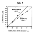
- A theoretical value of κL is varied depending on whether the diffraction grating has a rectangular shape or a sine wave shape, and value of κ in a diffraction grating having a sine wave shape can be reduced. FIG. 5 depicts simulation results of a relation between the height of the diffraction grating and KL depending on a difference in shape of the diffraction grating. Note that KL is relative value. It is assumed herein that a composition wavelength (λ) of the InGaAsP diffraction grating layer is 1.15 µm, and the oscillator length (L) is 500 µm. A primary component in a result of Fourier transform of a cross-section shape of the diffraction grating in the waveguide direction considered as a periodic waveform affects the magnitude of KL. Therefore, such a phenomenon as depicted in the drawing occurs. According to this result, by forming the diffraction grating in a sine wave shape, KL can be reduced by 21.5% (π/4) compared with the case of a rectangular shape. Usually, a diffraction grating is formed through dry etching or wet etching. In this case, a shape of the diffraction grating become rectangular, and it is difficult to form a sine wave shape through etching. This sine wave shape can be formed through thermal decomposition at increase of temperature in burying regrowth. In this case, however, the above-mentioned problem occurs due to mass transport.
- As has been descried above, in the conventional semiconductor laser device manufacturing technology, the lower limit of height of the diffraction grating is determined by the restrictions in the diffraction grating forming process, thereby it is difficult to reduce the value of κ. Also, a reactive product is formed on side surfaces and the trench portions of the diffraction grating in a process of an increase of temperature in burying regrowth of the diffraction grating, and causes deterioration of oscillation threshold and optical output efficiency of the device.
- An object of the present invention is to overcome the above-described problems, and to provide a semiconductor laser device manufacturing technology capable of reducing κL with manufacturing restrictions satisfied.
- The above and other objects as well as novel features of the present invention will be readily apparent from the description of the specification and accompanying drawings.
- The outline of a representative one of the inventions to be disclosed in the present application is briefly explained as below.
- The present invention is applied to a distributed-feedback or distributed-reflective semiconductor laser device having diffraction gratings formed in stripes perpendicular to a waveguide direction, and characterized by that each diffraction grating has side walls each having at least two or more crystal faces, and a ratio of length of an upper side to a bottom side of the diffraction grating, in a waveguide direction parallel to a (100) surface, is 0 to 0.3.
- Furthermore, the diffraction grating is formed of III-V family compound semiconductor layer including at least one of In, Ga, As, and P elements.
- Still further, immediately before burying regrowth of the diffraction grating, halogen-based gas is introduced to a reactor, and etching process is performed to the diffraction grating to have the above-described shape. And a reactive product, formed on side surfaces of the diffraction grating and in trench portions between stripes at an increase of temperature in regrowth, is removed.
- The effects achieved by a representative one of the inventions to be disclosed in the present application is briefly explained as below.
- According to the present invention, in the semiconductor laser device having the diffraction grating, a value of KL can be reduced with manufacturing restrictions satisfied. Furthermore, with an effect that the reactive product deteriorated in crystallinity on a regrowth surface is removed, an improvement of the optical output efficiency of the semiconductor laser device and a reduction of oscillation threshold can be achieved.
-
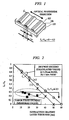
- FIG. 1 is a drawing describing a diffraction grating having a sine wave shape in a semiconductor laser device according to a preferred embodiment of the present invention.
- FIG. 2 is a drawing describing a relation between a thickness of diffraction grating layer and L1/L0 corresponding to an etching method in the semiconductor laser device according to a preferred embodiment of the present invention.
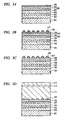
- FIG. 3A is a drawing that depicts a method of manufacturing a semiconductor laser device according to a first preferred embodiment of the present invention.
- FIG. 3B is a drawing that depicts a method of manufacturing a semiconductor laser device according to a first preferred embodiment of the present invention.
- FIG. 3C is a drawing that depicts a method of manufacturing a semiconductor laser device according to a first preferred embodiment of the present invention.
- FIG. 3D is a drawing that depicts a method of manufacturing a semiconductor laser device according to a first preferred embodiment of the present invention.
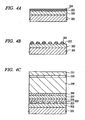
- FIG. 4A is a drawing that depicts a method of manufacturing a semiconductor laser device according to a second preferred embodiment of the present invention.
- FIG. 4B is a drawing that depicts a method of manufacturing a semiconductor laser device according to a second preferred embodiment of the present invention.
- FIG. 4C is a drawing that depicts a method of manufacturing a semiconductor laser device according to a second preferred embodiment of the present invention.
- FIG. 5 is a drawing describing a relation between a height of a diffraction grating layer and κL corresponding to a shape of a diffraction grating of a semiconductor laser device in problems to be solved by the invention.
- Embodiments according to the present invention are described in detail below based on the drawings. Here, for description of the embodiments, in all drawings, the same components are provided with the same symbols, and are not repeatedly described herein.
- In the present embodiment, in order to reduce the value of κ, as a first means, the diffraction grating after regrowth of a second clad layer is made to have a sine wave shape. Ideally, the sine wave shape is represented by a perfect sine curve. In actuality, however, the sine wave shape is in a state that a rectangular shape remains to some extent.
- Here, as parameters that represent a sine wave shape, as shown in FIG. 1, a ratio (L1/L0) of an upper side (L1) to a bottom side (L0) parallel to a (100) surface in diffraction gratings (diffraction grating layers 107), which formed in stripes perpendicular to a optical waveguide direction have side walls each having at least two or more crystal faces, is defined. If L1/L0 is 1, the shape of the diffraction grating is a square. If L1/L0 is 0, the shape is a triangle. If L1/L0 is equal to or smaller than 0.3, the shape can nearly approximate to a sine wave. Therefore, it can be said that the sine wave shape is achieved when L1/L0 is 0 to 0.3.
- To realize this first means, in-situ vapor phase etching introducing halogen-based gas to a reactor is performed after setting the height of the diffraction grating after dry and wet etching at 20 to 30 nm which has sufficient process controllability and increasing the temperature to a regrowth temperature of a clad layer.
- As shown in FIG. 2, if the diffraction grating is formed through dry and wet etching, the height of the diffraction grating has to be 35nm to 45 nm to achieve L1/L0 equal to or smaller than 0.3 attaining a sine wave shape. With that height, the value of κL becomes larger. The reason for this relation is that since only one crystal face appears through anisotropic wet etching, the relation is uniquely determined by the height of the diffraction grating layer and the bottom side length.
- By contrast, when vapor phase etching is applied, two or more crystal faces appear by etching the side walls of the diffraction grating layer. Therefore, even with the height of 15nm to 30 nm, L1/L0 can be equal to or smaller than 0.3. With this scheme, the thickness of diffraction grating after burying regrowth is reduced to 15 nm or lower, which has been difficult with the conventional process, and a sine wave shape can be easily achieved.
- Furthermore, this scheme has an effect of cleaning, that is, the reactive product formed due to mass transport at an increase of temperature is removed with halogen-based gas. Therefore, not only improving optical output by reducing K, but also oscillation threshold current and device reliability can be improved.
- As a second means, to facilitate the above-described vapor phase etching, the diffraction grating is formed of a III-V family compound semiconductor layer including at least one of In, Ga, As, and P elements.
- FIG. 3 is a drawing that shows a process chart of a semiconductor laser device manufacturing method according to a first embodiment of the present invention.
- On an n-
InP substrate 101, an n-InP first cladlayer 102, an n-InGaAlAs firstoptical guide layer 103, an InGaAlAsactive layer 104, a p-InGaAlAs secondoptical guide layer 105, a p-InP spacer layer 106, a p-InGaAsPdiffraction grating layer 107, and a p-InP cap layer 108 are laminated through MOCVD (FIG. 3A). To enhance a carrier confinement effect, the InGaAlAsactive layer 104 has an MQW configuration consisted of an InGaAlAs barrier layer and InGaAlAs well layer. Also, in consideration of controllability over a process of forming a diffraction grating, the diffraction grating layer is made to have a film thickness of 25 nm. - Next, through CVD, an insulating
film 109, such as a silicon dioxide (SiO2) film or a silicon nitride (SiN) film and the like, is formed. After a resistfilm 110 is applied, stripes with a period of approximately 200 nm in a direction perpendicular to a waveguide is formed through EB exposure or interference exposure. Using this resistfilm 110 as a mask, portions of the insulatingfilm 109 at openings are then removed through chemical etching. Chemical etching may be either one of wet etching using hydrofluoric acid mixed solution and dry etching using fluorinated gas (FIG. 3B). - Then, after removing the resist
film 110 with solvent, portions of the p-InP cap layer 108 and the p-InGaAsPdiffraction grating layer 107 at openings are removed through dry etching using the insulatingfilm 109 as a mask. By using dry etching, better controllability in a depth direction can be achieved compared with wet etching. Furthermore, etching is performed in a perpendicular shape from end of a mask of the insulating film. Therefore, controllability over a duty ratio of the diffraction grating is improved, and controllability over K is also improved. Then, the insulatingfilm 109 is removed with hydrofluoric acid mixed solution. With the process so far, a rectangular-shaped diffraction grating including the p-InP cap layer on the active layer served as a waveguide is formed (FIG. 3C). - Next, a surface treatment is performed on the diffraction grating formation substrate with sulfuric acid mixed solution. Then, through MOCVD, on the above-mentioned substrate, regrowth of a p-InP second clad
layer 111, a p-InGaAsPfirst contact layer 112, and a p-InGaAssecond contact layer 113 is performed. Here, immediately before regrowth of the p-InP second cladlayer 111, hydrochloric acid (HC1) gas is supplied to the reactor to perform in-situ vapor phase etching on the surface of the p-InP cap layer 108 and the p-InGaAsP diffraction grating layer 107 (FIG. 3D). At etching process, temperature of the substrate surface is set at 500 °C, and the etching time is set so that the height of the diffraction grating is 13 nm. - In this vapor phase etching, it is possible to remove reactive product with deteriorated crystallinity, formed on the side surfaces and trench portions of the diffraction grating due to mass transport from the p-
InP cap layer 108 in the process of increasing temperature. With this, a leak current caused by such a reactive product can be suppressed and an oscillation threshold of the semiconductor laser device can be reduced. Furthermore, by partially etching the p-InGaAsPdiffraction grating layer 107, the height of the diffraction grating is reduced, and a sine wave shape can be achieved. Thus, value of K is reduced, and optical output efficiency is improved. - Here, in the present embodiment, HCl is used for etching of the diffraction grating formation ,substrate. Alternatively, halogen-based gas containing a halogen element, such as methyl chloride (CH3Cl), carbon tetrachloride (CCl4), or carbon tetrabromide (CBr4), can be used.
- After burying regrowth to the diffraction grating formation substrate, processes using known technology described below is performed until chip making, thus, a semiconductor laser device is manufactured.
- First, stripes of approximately 2 µm made of insulating film are formed. Using the insulating film as a mask, the regrowth layer is removed through wet etching and dry etching to form an optical waveguide. After removing the stripe-shaped insulating film, an insulating film is formed again on the entire surface. Then, only a current injecting portion of the optical waveguide is opened through photolithography and etching, and then EB vapor deposition and heat treatment are performed to form a p-side electrode. After polishing the back surface of the substrate to a thickness of 100 µm, an n-side electrode is formed on the back surface through vapor deposition. After that, a wafer is cut open in a bar shape so that the oscillator length (L) is 500 µm. Then, through spattering, an end face is coated with a reflective film. Finally, the substrate is made into a chip having device with width of 200 µm, thus, a DFB semiconductor laser device is manufactured.
- Through in-situ vapor phase etching using halogen-based gas immediately before regrowth of the p-InP second clad
layer 111 according to the embodiment, a reactive product with deteriorated crystallinity, formed in the trench portions of the diffraction grating due to mass transport at an increase of temperature for regrowth, is removed. Furthermore a sine wave shape can be achieved with a reduced height of the diffraction grading. With this, an effect of cleaning of the regrowth interface can be achieved. Still further, by achieving reduction of κL n the semiconductor laser device, an oscillation threshold of 3mA is reduced. According to the present embodiment, a device characteristic yield, 70% in conventional, is improved to 90 %. - FIG. 4 is a drawing that shows a process chart of a semiconductor laser device manufacturing method according to a second embodiment of the present invention. In this embodiment, a method of manufacturing a semiconductor laser device, in which a diffraction grating is disposed on a lower side of an active layer, is described.
- On an n-
InP substrate 201, an n-InP first cladlayer 202, an n-InGaAlAsPdiffraction grating layer 203, and an n-InP cap layer 204 are laminated through MOCVD (FIG. 4A). Here, the n-InGaAsPdiffraction grating layer 203 is made to have a film thickness of 25nm, similar to that of the first embodiment. - Next, an insulating film is formed through CVD and, a diffraction grating is formed using a process similar to that of the first embodiment (FIG. 4B).
- After that, through MOCVD, burying regrowth of the diffraction grating is performed. Immediately before regrowth, as with the first embodiment, halogen-based gas is supplied so that the side surfaces and the trench portions of the diffraction grating are etched. Then, an n-InP second clad
layer 205, an n-InGaAlAs firstoptical guide layer 206, an InGaAlAsactive layer 207, a p-InGaAlAs secondoptical guide layer 208, a p-InP thirdclad layer 209, a p-InGaAsPfirst contact layer 210, and a p-InGaAssecond contact layer 211 are successively deposited (FIG. 4C). - After that, from a mesa formation process to chip making, a procedure similar to that in the first embodiment is performed. Also in the present embodiment, the device characteristic yield, 60% in conventional, is improved to 90%.
- Thus, while the invention carried out by the present inventors have been specifically described based on the embodiment, the present invention is not limited to the above described embodiment, but it goes without saying that various modifications are possible within the scope of the invention.
- The present invention relates to a semiconductor laser device and manufacturing technology thereof, and particularly to a technology effective when applied to a distributed-feedback or distributed-reflective semiconductor laser device for use in apparatuses for optical transmission or for information storage, and a method of manufacturing such a semiconductor laser device.
Claims (8)
- A distributed-feedback or distributed-reflective semiconductor laser device comprising:a diffraction grating formed in stripes perpendicular to a waveguide direction,wherein the diffraction grating (107) has side walls each having at least two or more crystal faces, and a ratio of length of an upper side (L1) in a waveguide direction to a bottom side (L0) parallel to a [100] surface is 0 to 0.3.
- The semiconductor laser device according to claim 1,
wherein the diffraction grating (107) is composed of a III-V family compound semiconductor layer including at least one of In, Ga, As, and P elements. - A method of manufacturing semiconductor laser device comprising:a first step of laminating a first clad layer (102), an active layer (104), and a diffraction grating layer (107) on a semiconductor substrate (101) through epitaxial growth;a second step of forming a diffraction grating by etching the diffraction grating layer (107); anda third step of performing burying regrowth of the diffraction grating through epitaxial growth on a second clad layer (111) of different conduction type from the first clad layer (102),wherein immediately before the third step, halogen-based gas is introduced to a reactor, and etching is performed on the diffraction grating so that each side wall has at least two or more crystal faces and a ratio of length of an upper side (L1) in a waveguide direction to a bottom side (L0) parallel to a [100] surface is 0 to 0.3, and a reactive product formed on side surfaces of the diffraction grating and in trench portions between stripes of the diffraction grating at an increase in temperature for regrowth is removed.
- The method of manufacturing semiconductor laser device according to claim 3,
wherein in the first step, a first optical guide layer (103) is further formed between the first clad layer (102) and the active layer (104), and a second optical guide layer (105) and a spacer layer (106) are formed between the active layer (104) and the diffraction grating layer (107). - The method of manufacturing semiconductor laser device according to claim 3,
wherein the diffraction grating layer (107) is a III-V family compound semiconductor layer including at least one of In, Ga, As, and P elements. - A method of manufacturing semiconductor laser device comprising:a first step of laminating, through epitaxial growth, a first clad layer (202) and a diffraction grating layer (203) on a semiconductor substrate (201);a second step of forming a diffraction grating through etching on the diffraction grating layer (203); anda third step of burying the diffraction grating through epitaxial growth on a second clad layer (205) of identical conduction type to the first clad layer (202) for regrowth of the active layer (207),wherein immediately before the third step, halogen-based gas is introduced to a reactor, etching is performed on the diffraction grating so that each side wall has at least two or more crystal faces and a ratio of length of an upper side (L1) in a waveguide direction to a bottom side (L0) parallel to a [100] surface is 0 to 0.3, and a reactive product formed on side surfaces of the diffraction grating and in trench portions between stripes of the diffraction grating at an increase in temperature for regrowth is removed.
- The method of manufacturing semiconductor laser device according to claim 6,
wherein in the third step, a first optical guide layer (206) is further formed between the second clad layer (205) and the active layer (207), and a second optical guide layer (208) and a third clad layer (209) are formed on an upper portion of the active layer (207). - The method of manufacturing semiconductor laser device according to claim 6,
wherein the diffraction grating layer is a III-V family compound semiconductor layer including at least one of In, Ga, As, and P elements.
Applications Claiming Priority (1)
| Application Number | Priority Date | Filing Date | Title |
|---|---|---|---|
| JP2006122777A JP4951267B2 (en) | 2006-04-27 | 2006-04-27 | Manufacturing method of semiconductor laser device |
Publications (3)
| Publication Number | Publication Date |
|---|---|
| EP1850430A2 true EP1850430A2 (en) | 2007-10-31 |
| EP1850430A3 EP1850430A3 (en) | 2009-12-16 |
| EP1850430B1 EP1850430B1 (en) | 2013-05-01 |
Family
ID=38442608
Family Applications (1)
| Application Number | Title | Priority Date | Filing Date |
|---|---|---|---|
| EP07003455.8A Active EP1850430B1 (en) | 2006-04-27 | 2007-02-19 | Method of manufacturing a semiconductor laser device |
Country Status (3)
| Country | Link |
|---|---|
| US (2) | US20080013582A1 (en) |
| EP (1) | EP1850430B1 (en) |
| JP (1) | JP4951267B2 (en) |
Cited By (1)
| Publication number | Priority date | Publication date | Assignee | Title |
|---|---|---|---|---|
| CN106785905A (en) * | 2017-01-19 | 2017-05-31 | 桂林电子科技大学 | A kind of electrooptic modulator based on Prague phase-shifted grating |
Families Citing this family (5)
| Publication number | Priority date | Publication date | Assignee | Title |
|---|---|---|---|---|
| KR100958719B1 (en) * | 2007-12-12 | 2010-05-18 | 한국전자통신연구원 | Hybrid Laser Diode For Single Mode Operation And Method Of Fabricating The Same |
| DE102008054217A1 (en) * | 2008-10-31 | 2010-05-06 | Osram Opto Semiconductors Gmbh | Optoelectronic semiconductor chip and method for producing an optoelectronic semiconductor chip |
| JP5206976B2 (en) * | 2009-03-06 | 2013-06-12 | 富士通株式会社 | Semiconductor laser and manufacturing method thereof |
| CN104201566B (en) * | 2014-08-22 | 2017-12-29 | 华中科技大学 | Ridge waveguide distributed feedback semiconductor laser with high single longitudinal mode yield |
| US11133649B2 (en) * | 2019-06-21 | 2021-09-28 | Palo Alto Research Center Incorporated | Index and gain coupled distributed feedback laser |
Citations (2)
| Publication number | Priority date | Publication date | Assignee | Title |
|---|---|---|---|---|
| JPS62150794A (en) | 1985-12-24 | 1987-07-04 | Sony Corp | Distributed-feedback type semiconductor laser |
| JPH098396A (en) | 1995-06-19 | 1997-01-10 | Nec Corp | Distributed feedback semiconductor laser element |
Family Cites Families (15)
| Publication number | Priority date | Publication date | Assignee | Title |
|---|---|---|---|---|
| JPS63265485A (en) * | 1987-04-23 | 1988-11-01 | Sony Corp | Semiconductor laser |
| JPS6454790A (en) * | 1987-08-26 | 1989-03-02 | Matsushita Electric Ind Co Ltd | Distributed feedback type semiconductor laser |
| JP3204474B2 (en) * | 1993-03-01 | 2001-09-04 | キヤノン株式会社 | Gain-coupled distributed feedback semiconductor laser and its fabrication method |
| JP3374878B2 (en) * | 1994-09-02 | 2003-02-10 | 三菱電機株式会社 | Semiconductor etching method |
| JP3751052B2 (en) * | 1994-12-28 | 2006-03-01 | シャープ株式会社 | Integrated light control element and method for manufacturing the same, and optical integrated circuit element and optical integrated circuit device including the same |
| US5633193A (en) * | 1996-05-22 | 1997-05-27 | Lucent Technologies Inc. | Method of making an InP-based device comprising semiconductor growth on a non-planar surface |
| JP3643486B2 (en) * | 1998-08-04 | 2005-04-27 | 株式会社東芝 | Optical functional device and optical communication system |
| EP1043818B1 (en) * | 1999-04-09 | 2011-07-20 | Mitsui Chemicals, Inc. | Semiconductor laser device, semiconductor laser module, rare-earth-element-doped optical fiber amplifier and fiber laser |
| US7016391B2 (en) * | 2000-03-13 | 2006-03-21 | Sharp Kabushiki Kaisha | Gain-coupled distributed feedback semiconductor laser device and production method therefor |
| JP2001266389A (en) * | 2000-03-23 | 2001-09-28 | Tdk Corp | Optical head using near field light |
| JP4031263B2 (en) * | 2002-03-05 | 2008-01-09 | 三菱電機株式会社 | Manufacturing method of semiconductor laser device |
| US6608855B1 (en) * | 2002-05-31 | 2003-08-19 | Applied Optoelectronics, Inc. | Single-mode DBR laser with improved phase-shift section |
| JP2005129833A (en) * | 2003-10-27 | 2005-05-19 | Nec Kansai Ltd | Method of manufacturing semiconductor laser |
| JP4164438B2 (en) * | 2003-11-12 | 2008-10-15 | 株式会社日立製作所 | Semiconductor optical device manufacturing method |
| JP2006108278A (en) * | 2004-10-04 | 2006-04-20 | Matsushita Electric Ind Co Ltd | Semiconductor laser |
-
2006
- 2006-04-27 JP JP2006122777A patent/JP4951267B2/en active Active
-
2007
- 2007-02-19 EP EP07003455.8A patent/EP1850430B1/en active Active
- 2007-02-20 US US11/708,135 patent/US20080013582A1/en not_active Abandoned
-
2009
- 2009-10-02 US US12/572,720 patent/US7855093B2/en active Active
Patent Citations (2)
| Publication number | Priority date | Publication date | Assignee | Title |
|---|---|---|---|---|
| JPS62150794A (en) | 1985-12-24 | 1987-07-04 | Sony Corp | Distributed-feedback type semiconductor laser |
| JPH098396A (en) | 1995-06-19 | 1997-01-10 | Nec Corp | Distributed feedback semiconductor laser element |
Cited By (1)
| Publication number | Priority date | Publication date | Assignee | Title |
|---|---|---|---|---|
| CN106785905A (en) * | 2017-01-19 | 2017-05-31 | 桂林电子科技大学 | A kind of electrooptic modulator based on Prague phase-shifted grating |
Also Published As
| Publication number | Publication date |
|---|---|
| JP4951267B2 (en) | 2012-06-13 |
| EP1850430A3 (en) | 2009-12-16 |
| JP2007294774A (en) | 2007-11-08 |
| EP1850430B1 (en) | 2013-05-01 |
| US20080013582A1 (en) | 2008-01-17 |
| US7855093B2 (en) | 2010-12-21 |
| US20100022043A1 (en) | 2010-01-28 |
Similar Documents
| Publication | Publication Date | Title |
|---|---|---|
| US5982804A (en) | Non-regrowth distributed feedback ridge semiconductor laser and method of manufacturing the same | |
| US6292503B1 (en) | Ridge type semiconductor laser of laterally-coupled distributed feedback and method of manufacturing the same | |
| US8705583B2 (en) | Semiconductor laser | |
| Nunoya et al. | High-performance 1.55-/spl mu/m wavelength GaInAsP-InP distributed-feedback lasers with wirelike active regions | |
| US8494320B2 (en) | Optical element and method for manufacturing the same | |
| JP5280614B2 (en) | Embedded heterostructure devices incorporating waveguide gratings fabricated by single step MOCVD | |
| US7855093B2 (en) | Semiconductor laser device and method of manufacturing the same | |
| JP3842976B2 (en) | Distributed feedback semiconductor laser and manufacturing method thereof | |
| US8637338B2 (en) | Method for producing integrated optical device | |
| JP3204474B2 (en) | Gain-coupled distributed feedback semiconductor laser and its fabrication method | |
| US7957446B2 (en) | Semiconductor laser and method of making semiconductor laser | |
| WO2007072807A1 (en) | Semiconductor element and method for manufacturing semiconductor element | |
| JP3450169B2 (en) | Distributed feedback semiconductor laser | |
| JP2007184491A (en) | Distributed feedback semiconductor laser | |
| Park et al. | Low-threshold loss-coupled laser diode by new grating fabrication technique | |
| JP5217767B2 (en) | Semiconductor laser and method for manufacturing semiconductor laser | |
| JP4151043B2 (en) | Manufacturing method of optical semiconductor device | |
| US8846425B2 (en) | Diode laser and method for manufacturing a high-efficiency diode laser | |
| JP2002057405A (en) | Semiconductor laser device and its manufacturing method | |
| JP4992451B2 (en) | Semiconductor laser and method of manufacturing the semiconductor laser | |
| JP3455404B2 (en) | Semiconductor optical device and manufacturing method thereof | |
| JPH0642583B2 (en) | Semiconductor laser device | |
| JP2001168455A (en) | Manufacturing method for optical semiconductor device | |
| JP2810518B2 (en) | Semiconductor laser device and method of manufacturing the same | |
| JPH11195836A (en) | Semiconductor light element, and its manufacture |
Legal Events
| Date | Code | Title | Description |
|---|---|---|---|
| PUAI | Public reference made under article 153(3) epc to a published international application that has entered the european phase |
Free format text: ORIGINAL CODE: 0009012 |
|
| AK | Designated contracting states |
Kind code of ref document: A2 Designated state(s): AT BE BG CH CY CZ DE DK EE ES FI FR GB GR HU IE IS IT LI LT LU LV MC NL PL PT RO SE SI SK TR |
|
| AX | Request for extension of the european patent |
Extension state: AL BA HR MK YU |
|
| PUAL | Search report despatched |
Free format text: ORIGINAL CODE: 0009013 |
|
| AK | Designated contracting states |
Kind code of ref document: A3 Designated state(s): AT BE BG CH CY CZ DE DK EE ES FI FR GB GR HU IE IS IT LI LT LU LV MC NL PL PT RO SE SI SK TR |
|
| AX | Request for extension of the european patent |
Extension state: AL BA HR MK RS |
|
| 17P | Request for examination filed |
Effective date: 20100107 |
|
| 17Q | First examination report despatched |
Effective date: 20100209 |
|
| AKX | Designation fees paid |
Designated state(s): DE FR GB |
|
| GRAP | Despatch of communication of intention to grant a patent |
Free format text: ORIGINAL CODE: EPIDOSNIGR1 |
|
| GRAC | Information related to communication of intention to grant a patent modified |
Free format text: ORIGINAL CODE: EPIDOSCIGR1 |
|
| RAP1 | Party data changed (applicant data changed or rights of an application transferred) |
Owner name: OCLARO JAPAN, INC. |
|
| GRAP | Despatch of communication of intention to grant a patent |
Free format text: ORIGINAL CODE: EPIDOSNIGR1 |
|
| RIN1 | Information on inventor provided before grant (corrected) |
Inventor name: WASHINO, RYU C/O OCLARO JAPAN, INC. Inventor name: KOMATSU, KAZUHIRO C/O OCLARO JAPAN, INC. Inventor name: OKAMOTO, KAORU C/O OCLARO JAPAN, INC. Inventor name: SAKUMA, YASUSHI C/O OCLARO JAPAN, INC. |
|
| RIN1 | Information on inventor provided before grant (corrected) |
Inventor name: WASHINO, RYU Inventor name: SAKUMA, YASUSHI Inventor name: KOMATSU, KAZUHIRO Inventor name: OKAMOTO, KAORU |
|
| GRAS | Grant fee paid |
Free format text: ORIGINAL CODE: EPIDOSNIGR3 |
|
| GRAA | (expected) grant |
Free format text: ORIGINAL CODE: 0009210 |
|
| AK | Designated contracting states |
Kind code of ref document: B1 Designated state(s): DE FR GB |
|
| REG | Reference to a national code |
Ref country code: GB Ref legal event code: FG4D |
|
| REG | Reference to a national code |
Ref country code: DE Ref legal event code: R096 Ref document number: 602007030109 Country of ref document: DE Effective date: 20130627 |
|
| PLBE | No opposition filed within time limit |
Free format text: ORIGINAL CODE: 0009261 |
|
| STAA | Information on the status of an ep patent application or granted ep patent |
Free format text: STATUS: NO OPPOSITION FILED WITHIN TIME LIMIT |
|
| 26N | No opposition filed |
Effective date: 20140204 |
|
| REG | Reference to a national code |
Ref country code: DE Ref legal event code: R097 Ref document number: 602007030109 Country of ref document: DE Effective date: 20140204 |
|
| REG | Reference to a national code |
Ref country code: DE Ref legal event code: R082 Ref document number: 602007030109 Country of ref document: DE Representative=s name: BEETZ & PARTNER MBB, DE |
|
| REG | Reference to a national code |
Ref country code: FR Ref legal event code: CA Effective date: 20150424 |
|
| REG | Reference to a national code |
Ref country code: DE Ref legal event code: R082 Ref document number: 602007030109 Country of ref document: DE Representative=s name: BEETZ & PARTNER MBB, DE Effective date: 20150427 Ref country code: DE Ref legal event code: R081 Ref document number: 602007030109 Country of ref document: DE Owner name: OCLARO JAPAN, INC., SAGAMIHARA, JP Free format text: FORMER OWNER: OCLARO JAPAN, INC., YOKOHAMA-SHI, KANAGAWA, JP Effective date: 20150427 Ref country code: DE Ref legal event code: R081 Ref document number: 602007030109 Country of ref document: DE Owner name: OCLARO JAPAN, INC., SAGAMIHARA, JP Free format text: FORMER OWNER: OPNEXT JAPAN, INC., YOKOHAMA, KANAGAWA, JP Effective date: 20130503 Ref country code: DE Ref legal event code: R082 Ref document number: 602007030109 Country of ref document: DE Representative=s name: BEETZ & PARTNER MBB PATENTANWAELTE, DE Effective date: 20150427 Ref country code: DE Ref legal event code: R082 Ref document number: 602007030109 Country of ref document: DE Representative=s name: BEETZ & PARTNER MBB PATENT- UND RECHTSANWAELTE, DE Effective date: 20150427 |
|
| REG | Reference to a national code |
Ref country code: FR Ref legal event code: PLFP Year of fee payment: 10 |
|
| REG | Reference to a national code |
Ref country code: FR Ref legal event code: PLFP Year of fee payment: 11 |
|
| REG | Reference to a national code |
Ref country code: FR Ref legal event code: PLFP Year of fee payment: 12 |
|
| REG | Reference to a national code |
Ref country code: DE Ref legal event code: R082 Ref document number: 602007030109 Country of ref document: DE Representative=s name: BEETZ & PARTNER MBB PATENT- UND RECHTSANWAELTE, DE Ref country code: DE Ref legal event code: R081 Ref document number: 602007030109 Country of ref document: DE Owner name: LUMENTUM JAPAN, INC., SAGAMIHARA, JP Free format text: FORMER OWNER: OCLARO JAPAN, INC., SAGAMIHARA, KANAGAWA, JP Ref country code: DE Ref legal event code: R082 Ref document number: 602007030109 Country of ref document: DE Representative=s name: BEETZ & PARTNER MBB PATENTANWAELTE, DE |
|
| PGFP | Annual fee paid to national office [announced via postgrant information from national office to epo] |
Ref country code: FR Payment date: 20230223 Year of fee payment: 17 |
|
| PGFP | Annual fee paid to national office [announced via postgrant information from national office to epo] |
Ref country code: GB Payment date: 20230227 Year of fee payment: 17 Ref country code: DE Payment date: 20230227 Year of fee payment: 17 |