EP1849167B1 - Dünnfilmwiderstand mit einer Stromdichteverstärkungsschicht - Google Patents
Dünnfilmwiderstand mit einer Stromdichteverstärkungsschicht Download PDFInfo
- Publication number
- EP1849167B1 EP1849167B1 EP06720491A EP06720491A EP1849167B1 EP 1849167 B1 EP1849167 B1 EP 1849167B1 EP 06720491 A EP06720491 A EP 06720491A EP 06720491 A EP06720491 A EP 06720491A EP 1849167 B1 EP1849167 B1 EP 1849167B1
- Authority
- EP
- European Patent Office
- Prior art keywords
- layer
- thin
- resistor
- cdel
- thin film
- Prior art date
- Legal status (The legal status is an assumption and is not a legal conclusion. Google has not performed a legal analysis and makes no representation as to the accuracy of the status listed.)
- Active
Links
- 239000010409 thin film Substances 0.000 title claims abstract description 57
- 239000000463 material Substances 0.000 claims abstract description 32
- 238000000034 method Methods 0.000 claims abstract description 21
- 239000004020 conductor Substances 0.000 claims abstract description 13
- 230000002708 enhancing effect Effects 0.000 claims abstract description 10
- 229910052751 metal Inorganic materials 0.000 claims description 21
- 239000002184 metal Substances 0.000 claims description 21
- 239000004065 semiconductor Substances 0.000 claims description 13
- PNEYBMLMFCGWSK-UHFFFAOYSA-N aluminium oxide Inorganic materials [O-2].[O-2].[O-2].[Al+3].[Al+3] PNEYBMLMFCGWSK-UHFFFAOYSA-N 0.000 claims description 11
- 229910052593 corundum Inorganic materials 0.000 claims description 11
- 229910001845 yogo sapphire Inorganic materials 0.000 claims description 11
- 238000004519 manufacturing process Methods 0.000 abstract description 9
- 239000012212 insulator Substances 0.000 abstract 1
- 239000003989 dielectric material Substances 0.000 description 17
- 230000035882 stress Effects 0.000 description 12
- 239000010408 film Substances 0.000 description 11
- VYPSYNLAJGMNEJ-UHFFFAOYSA-N Silicium dioxide Chemical compound O=[Si]=O VYPSYNLAJGMNEJ-UHFFFAOYSA-N 0.000 description 9
- 238000000231 atomic layer deposition Methods 0.000 description 8
- 238000005137 deposition process Methods 0.000 description 8
- 238000001465 metallisation Methods 0.000 description 8
- 238000000151 deposition Methods 0.000 description 7
- 230000004888 barrier function Effects 0.000 description 6
- 238000000623 plasma-assisted chemical vapour deposition Methods 0.000 description 6
- 229910021420 polycrystalline silicon Inorganic materials 0.000 description 6
- 229920005591 polysilicon Polymers 0.000 description 6
- PBCFLUZVCVVTBY-UHFFFAOYSA-N tantalum pentoxide Inorganic materials O=[Ta](=O)O[Ta](=O)=O PBCFLUZVCVVTBY-UHFFFAOYSA-N 0.000 description 6
- 238000005229 chemical vapour deposition Methods 0.000 description 5
- 239000010949 copper Substances 0.000 description 5
- 230000001681 protective effect Effects 0.000 description 5
- 239000000758 substrate Substances 0.000 description 5
- RYGMFSIKBFXOCR-UHFFFAOYSA-N Copper Chemical compound [Cu] RYGMFSIKBFXOCR-UHFFFAOYSA-N 0.000 description 4
- MCMNRKCIXSYSNV-UHFFFAOYSA-N Zirconium dioxide Chemical compound O=[Zr]=O MCMNRKCIXSYSNV-UHFFFAOYSA-N 0.000 description 4
- 229910052782 aluminium Inorganic materials 0.000 description 4
- XAGFODPZIPBFFR-UHFFFAOYSA-N aluminium Chemical compound [Al] XAGFODPZIPBFFR-UHFFFAOYSA-N 0.000 description 4
- 229910052681 coesite Inorganic materials 0.000 description 4
- 229910052802 copper Inorganic materials 0.000 description 4
- 229910052906 cristobalite Inorganic materials 0.000 description 4
- 238000005530 etching Methods 0.000 description 4
- BPUBBGLMJRNUCC-UHFFFAOYSA-N oxygen(2-);tantalum(5+) Chemical compound [O-2].[O-2].[O-2].[O-2].[O-2].[Ta+5].[Ta+5] BPUBBGLMJRNUCC-UHFFFAOYSA-N 0.000 description 4
- 239000000377 silicon dioxide Substances 0.000 description 4
- 229910052682 stishovite Inorganic materials 0.000 description 4
- 229910052905 tridymite Inorganic materials 0.000 description 4
- ATJFFYVFTNAWJD-UHFFFAOYSA-N Tin Chemical compound [Sn] ATJFFYVFTNAWJD-UHFFFAOYSA-N 0.000 description 3
- 230000032683 aging Effects 0.000 description 3
- 238000007796 conventional method Methods 0.000 description 3
- 238000001704 evaporation Methods 0.000 description 3
- 230000008020 evaporation Effects 0.000 description 3
- 150000004767 nitrides Chemical class 0.000 description 3
- 230000003647 oxidation Effects 0.000 description 3
- 238000007254 oxidation reaction Methods 0.000 description 3
- 238000002161 passivation Methods 0.000 description 3
- 229920003209 poly(hydridosilsesquioxane) Polymers 0.000 description 3
- 238000004544 sputter deposition Methods 0.000 description 3
- PXHVJJICTQNCMI-UHFFFAOYSA-N Nickel Chemical compound [Ni] PXHVJJICTQNCMI-UHFFFAOYSA-N 0.000 description 2
- 229910052581 Si3N4 Inorganic materials 0.000 description 2
- -1 Ta2O5 Chemical class 0.000 description 2
- BOTDANWDWHJENH-UHFFFAOYSA-N Tetraethyl orthosilicate Chemical compound CCO[Si](OCC)(OCC)OCC BOTDANWDWHJENH-UHFFFAOYSA-N 0.000 description 2
- 230000008021 deposition Effects 0.000 description 2
- CJNBYAVZURUTKZ-UHFFFAOYSA-N hafnium(IV) oxide Inorganic materials O=[Hf]=O CJNBYAVZURUTKZ-UHFFFAOYSA-N 0.000 description 2
- 239000011810 insulating material Substances 0.000 description 2
- 229910044991 metal oxide Inorganic materials 0.000 description 2
- 150000004706 metal oxides Chemical class 0.000 description 2
- 238000013508 migration Methods 0.000 description 2
- 230000005012 migration Effects 0.000 description 2
- 230000001590 oxidative effect Effects 0.000 description 2
- 238000007747 plating Methods 0.000 description 2
- HQVNEWCFYHHQES-UHFFFAOYSA-N silicon nitride Chemical compound N12[Si]34N5[Si]62N3[Si]51N64 HQVNEWCFYHHQES-UHFFFAOYSA-N 0.000 description 2
- JLTRXTDYQLMHGR-UHFFFAOYSA-N trimethylaluminium Chemical compound C[Al](C)C JLTRXTDYQLMHGR-UHFFFAOYSA-N 0.000 description 2
- VYZAMTAEIAYCRO-UHFFFAOYSA-N Chromium Chemical compound [Cr] VYZAMTAEIAYCRO-UHFFFAOYSA-N 0.000 description 1
- CBENFWSGALASAD-UHFFFAOYSA-N Ozone Chemical compound [O-][O+]=O CBENFWSGALASAD-UHFFFAOYSA-N 0.000 description 1
- 125000003118 aryl group Chemical group 0.000 description 1
- 230000015572 biosynthetic process Effects 0.000 description 1
- 230000015556 catabolic process Effects 0.000 description 1
- 238000000224 chemical solution deposition Methods 0.000 description 1
- 229910052804 chromium Inorganic materials 0.000 description 1
- 239000011651 chromium Substances 0.000 description 1
- VNNRSPGTAMTISX-UHFFFAOYSA-N chromium nickel Chemical compound [Cr].[Ni] VNNRSPGTAMTISX-UHFFFAOYSA-N 0.000 description 1
- 239000011248 coating agent Substances 0.000 description 1
- 238000000576 coating method Methods 0.000 description 1
- 230000003247 decreasing effect Effects 0.000 description 1
- 238000006731 degradation reaction Methods 0.000 description 1
- 239000012634 fragment Substances 0.000 description 1
- 239000011521 glass Substances 0.000 description 1
- 230000010354 integration Effects 0.000 description 1
- 239000007769 metal material Substances 0.000 description 1
- 150000002739 metals Chemical class 0.000 description 1
- 229910001120 nichrome Inorganic materials 0.000 description 1
- 229910052759 nickel Inorganic materials 0.000 description 1
- 150000001282 organosilanes Chemical class 0.000 description 1
- 239000007800 oxidant agent Substances 0.000 description 1
- 229920002120 photoresistant polymer Polymers 0.000 description 1
- 239000002952 polymeric resin Substances 0.000 description 1
- 239000002243 precursor Substances 0.000 description 1
- 229910052710 silicon Inorganic materials 0.000 description 1
- 229910052814 silicon oxide Inorganic materials 0.000 description 1
- 229920003002 synthetic resin Polymers 0.000 description 1
- 229910052715 tantalum Inorganic materials 0.000 description 1
- MZLGASXMSKOWSE-UHFFFAOYSA-N tantalum nitride Chemical compound [Ta]#N MZLGASXMSKOWSE-UHFFFAOYSA-N 0.000 description 1
- 229920001187 thermosetting polymer Polymers 0.000 description 1
- 238000009966 trimming Methods 0.000 description 1
Images


Classifications
-
- H—ELECTRICITY
- H01—ELECTRIC ELEMENTS
- H01L—SEMICONDUCTOR DEVICES NOT COVERED BY CLASS H10
- H01L28/00—Passive two-terminal components without a potential-jump or surface barrier for integrated circuits; Details thereof; Multistep manufacturing processes therefor
- H01L28/20—Resistors
- H01L28/24—Resistors with an active material comprising a refractory, transition or noble metal, metal compound or metal alloy, e.g. silicides, oxides, nitrides
-
- H—ELECTRICITY
- H01—ELECTRIC ELEMENTS
- H01C—RESISTORS
- H01C7/00—Non-adjustable resistors formed as one or more layers or coatings; Non-adjustable resistors made from powdered conducting material or powdered semi-conducting material with or without insulating material
- H01C7/006—Thin film resistors
-
- H—ELECTRICITY
- H01—ELECTRIC ELEMENTS
- H01L—SEMICONDUCTOR DEVICES NOT COVERED BY CLASS H10
- H01L27/00—Devices consisting of a plurality of semiconductor or other solid-state components formed in or on a common substrate
- H01L27/02—Devices consisting of a plurality of semiconductor or other solid-state components formed in or on a common substrate including semiconductor components specially adapted for rectifying, oscillating, amplifying or switching and having potential barriers; including integrated passive circuit elements having potential barriers
- H01L27/04—Devices consisting of a plurality of semiconductor or other solid-state components formed in or on a common substrate including semiconductor components specially adapted for rectifying, oscillating, amplifying or switching and having potential barriers; including integrated passive circuit elements having potential barriers the substrate being a semiconductor body
- H01L27/06—Devices consisting of a plurality of semiconductor or other solid-state components formed in or on a common substrate including semiconductor components specially adapted for rectifying, oscillating, amplifying or switching and having potential barriers; including integrated passive circuit elements having potential barriers the substrate being a semiconductor body including a plurality of individual components in a non-repetitive configuration
- H01L27/0611—Devices consisting of a plurality of semiconductor or other solid-state components formed in or on a common substrate including semiconductor components specially adapted for rectifying, oscillating, amplifying or switching and having potential barriers; including integrated passive circuit elements having potential barriers the substrate being a semiconductor body including a plurality of individual components in a non-repetitive configuration integrated circuits having a two-dimensional layout of components without a common active region
- H01L27/0617—Devices consisting of a plurality of semiconductor or other solid-state components formed in or on a common substrate including semiconductor components specially adapted for rectifying, oscillating, amplifying or switching and having potential barriers; including integrated passive circuit elements having potential barriers the substrate being a semiconductor body including a plurality of individual components in a non-repetitive configuration integrated circuits having a two-dimensional layout of components without a common active region comprising components of the field-effect type
- H01L27/0629—Devices consisting of a plurality of semiconductor or other solid-state components formed in or on a common substrate including semiconductor components specially adapted for rectifying, oscillating, amplifying or switching and having potential barriers; including integrated passive circuit elements having potential barriers the substrate being a semiconductor body including a plurality of individual components in a non-repetitive configuration integrated circuits having a two-dimensional layout of components without a common active region comprising components of the field-effect type in combination with diodes, or resistors, or capacitors
-
- H—ELECTRICITY
- H01—ELECTRIC ELEMENTS
- H01L—SEMICONDUCTOR DEVICES NOT COVERED BY CLASS H10
- H01L27/00—Devices consisting of a plurality of semiconductor or other solid-state components formed in or on a common substrate
- H01L27/02—Devices consisting of a plurality of semiconductor or other solid-state components formed in or on a common substrate including semiconductor components specially adapted for rectifying, oscillating, amplifying or switching and having potential barriers; including integrated passive circuit elements having potential barriers
- H01L27/04—Devices consisting of a plurality of semiconductor or other solid-state components formed in or on a common substrate including semiconductor components specially adapted for rectifying, oscillating, amplifying or switching and having potential barriers; including integrated passive circuit elements having potential barriers the substrate being a semiconductor body
- H01L27/06—Devices consisting of a plurality of semiconductor or other solid-state components formed in or on a common substrate including semiconductor components specially adapted for rectifying, oscillating, amplifying or switching and having potential barriers; including integrated passive circuit elements having potential barriers the substrate being a semiconductor body including a plurality of individual components in a non-repetitive configuration
- H01L27/0688—Integrated circuits having a three-dimensional layout
-
- H—ELECTRICITY
- H01—ELECTRIC ELEMENTS
- H01L—SEMICONDUCTOR DEVICES NOT COVERED BY CLASS H10
- H01L23/00—Details of semiconductor or other solid state devices
- H01L23/52—Arrangements for conducting electric current within the device in operation from one component to another, i.e. interconnections, e.g. wires, lead frames
- H01L23/522—Arrangements for conducting electric current within the device in operation from one component to another, i.e. interconnections, e.g. wires, lead frames including external interconnections consisting of a multilayer structure of conductive and insulating layers inseparably formed on the semiconductor body
- H01L23/5228—Resistive arrangements or effects of, or between, wiring layers
-
- H—ELECTRICITY
- H01—ELECTRIC ELEMENTS
- H01L—SEMICONDUCTOR DEVICES NOT COVERED BY CLASS H10
- H01L2924/00—Indexing scheme for arrangements or methods for connecting or disconnecting semiconductor or solid-state bodies as covered by H01L24/00
- H01L2924/0001—Technical content checked by a classifier
- H01L2924/0002—Not covered by any one of groups H01L24/00, H01L24/00 and H01L2224/00
Definitions
- the present invention relates generally to the field of semiconductor thin film resistors, and more particularly, to a novel integrated circuit thin film resistor having a current density enhancing layer.
- a resistor may be used to control the resistance of other electronic components of the IC.
- the resistance, R, of a resistor is proportional to the length, L, of the resistor and the reciprocal cross sectional area, I/A, of the resistor; the L and A are measured in the direction of current flow.
- Prior art resistors are typically composed of polysilicon that has been doped. As the integration of semiconductor devices increases, each component within a semiconductor IC has to provide equivalent or better electrical properties. A downscaled resistor thus has to provide a constant resistance value that does not fluctuate much during use. However, due to the properties of polysilicon, a prior art resistor comprised of doped polysilicon can only provide a limited resistance within a limited space. Employing a polysilicon resistor to provide relatively high resistance then becomes a problem in designing and fabricating a highly integrated semiconductor device.
- doped polysilicon resistors have been replaced with a single thin film resistor that is comprised of a material that has a higher resistivity than that of polysilicon.
- higher resistivity materials include, but are not limited to: TiN and TaN. Tantalum nitride, TaN, containing 36 % N 2 is a material currently being used in the back-end-of-the line (BEOL) of most semiconductor devices.
- BEOL resistors of high current carrying capability are highly desired by integrated circuit designers.
- Current TaN resistors e.g., Kl resistor
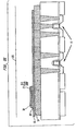
- Figure 1 depicts a BEOL resistor structure 10 according to the prior art.
- the BEOL resistor structure is formed atop of a first metallization level M1 comprising a metal such as aluminum or copper, that is electrically coupled by via structures V1, to FEOL device structures 15, e.g., CMOS FET or BJT or like transistor devices formed utilizing conventional techniques that are well known to those skilled in the art.
- the first metallization level M1 includes an interlevel dielectric material layer 12 in which the M1 metal layer structures are formed.
- typical fabrication processes as known in the art are used to form a further interlevel dielectric material layer and a via structure V1 that connects the first metallization to a second metallization level M2.
- the currently provided etch stop layer e.g., nBLOK (SiCN) or SiN, does not adhere well to the TaN film, and thus not as effective to prevent shifting of resistance during stress/aging.
- US 6703666 describes a thin film resistor comprising a resistive layer located on a first dielectric layer, first and second contact pads located on the resistive layer, and a second dielectric layer located over the resistive layer and the first and second contact pads.
- the thin film resistor further includes a first interconnect that contacts the first contact pad and a second interconnect that contacts the second contact pad.
- US 4288776 describes thin-film microcircuit structures passivated with silicon nitride are provided in which included electrical components containing nickel, chromium or other nitride-forming metals are encapsulated in an oxide material, preferably silicon oxide. The metal-containing components are thus prevented from reacting with the silicon nitride passivation coating during through-passivation laser trimming of the components.
- US 2002/0145503 describes a method of manufacturing a thin film resistor with a moisture barrier by depositing a metal film layer on a substrate and depositing a layer of tantalum pentoxide film overlaying the metal film layer. Also described is a thin film resistor having a substrate; a metal film layer attached to the substrate; and a tantalum pentoxide layer overlaying the metal film layer, the tantalum pentoxide layer providing a barrier to moisture, the tantalum pentoxide layer not overlaid by an oxidation process.
- a preferred embodiment of the invention provides a thin-film resistor for a semiconductor circuit structure comprising: a thin film layer of conductor material having a resistance value, said thin film layer of conductor material comprising TaN; a current density enhancing layer 'CDEL' formed on top of said thin film layer of conductor material, wherein said current density enhancing layer enables the said thin film resistor to carry higher current densities with reduced shift in resistance; characterised in that said current density enhancing layer comprises Al 2 O 3 , and has a thickness of less than 10nm.
- the Current Density Enhancement Layer provides increased resistance to shifting during stress/aging and further does not interfere with via etching process steps during BEOL or FEOL resistor fabrication.
- the CDEL barrier film in addition to SiN or SiCN cap materials over the TaN film, increases the current carrying capability of the resistor.
- the structure of the invention is applicable to manufacturing in both BEOL and FEOL processes.
- drawings of the present invention show a fragment of a semiconductor wafer or chip in which only one resistor device region is shown in a Back-End-Of-Line (BEOL) manufacturing process.
- BEOL Back-End-Of-Line
- the drawings show the presence of only a single resistor device region, the present processes, which do not from part of the invention, can be used in forming a plurality of resistors across different resistor device regions on the surface of a single semiconductor chip or wafer.
- the invention is applicable to front-end-of-line (FEOL) processes whereby the inventive resistor device structure is formed on a Si-containing substrate, for instance having other device regions including bipolar transistors and/or CMOS devices, such as FETs, that are formed to the periphery of the resistor device region shown in the drawings of the present application.
- FEOL front-end-of-line
- a first step involves depositing the interlevel dielectric layer 12, which may comprise a dielectric material such as a low-k organic or inorganic interlevel dielectric (ILD) of low-k dielectric material which may be deposited by any of number of well known techniques such as sputtering, spin-on, or PECVD and may include a conventional spun-on organic dielectrics, spun-on inorganic dielectrics or combinations thereof which have a dielectric constant of about 3.5 or less.
- Suitable organic dielectrics that can be employed include dielectrics that comprise C, O and H. Examples of some types of organic dielectrics that can be employed in the present invention include, but are not limited to: aromatic thermosetting polymeric resins, and other like organic dielectrics.
- the organic dielectric employed as interlevel dielectric layers may or may not be porous, with porous organic dielectric layers being highly preferred due to the reduced k value.
- Suitable inorganic dielectrics that may be employed as the interlevel dielectric typically comprise Si, O and H, and optionally C, e.g., SiO 2 , SiCOH, carbon-doped oxides (CDO), silicon-oxicarbides, organosilicate glasses (OSG) deposited by plasma enhanced chemical vapor deposition (CVD) techniques.
- Illustrative examples of some types of inorganic dielectrics include, but are not limited to: the silsesquioxane HOSP, methylsilsesquioxane (MSQ), hydrido silsesquioxane (HSQ), MSQ-HSQ copolymers, tetraethylorthosilicate (TEOS), organosilanes and any other Si-containing material.
- the interlevel dielectric material layer 12 is SiO 2 .
- the first metal layer M1 is formed at designed locations that connect with FEOL devices utilizing processes well known in the art.
- the M1 metal layer may comprise copper or aluminum.
- a protective dielectric layer 14 typically comprised of an inorganic dielectric that differs from a second dielectric layer 16 deposited on top of layer 14.
- the protective dielectric layer 14 is comprised of an oxide, nitride, oxynitride or any combination thereof, including multilayers.
- the protective dielectric layer 14 is typically a nitride such as SiN and the second dielectric layer 16 formed thereon is typically SiO 2 but could be other dielectrics such as SiCOH.
- the thickness of the protective dielectric layer 14 may vary depending on the type of material and deposition process employed in forming the same. Typically, the protective dielectric material has a thickness from about 10 ⁇ to about 1000 ⁇ .
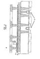
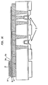
- a layer 20 of material forming the thin-film resistor is deposited atop the second dielectric layer 16.
- this layer 20 TaN may include other conductive metal materials including, but not limited must comprised to: Ta, Ti, TiN, W, WN, NiCr, SiCr, and the like, for forming the thin film resistor. Combinations of these materials are also contemplated herein.
- the conductive metal 20 is a thin layer whose thickness is typically from about 300 ⁇ to about 700 ⁇ with a thickness from about 450 ⁇ to about 550 ⁇ being more typical.
- the conductive metal 20 forming the thin-film resistor can be formed on the etch stop layer 14 utilizing any deposition process including, for example, CVD, PECVD, sputtering, plating, evaporation, ALD and other like deposition processes.
- a thin Current Density Enhancing Layer (CDEL) 50 is patterned and formed on the conductive metal 20 providing the structure shown, for example, in FIG. 2(a) .
- the CDEL layer 50 comprises Al 2 O 3 deposited to a thickness of less than 100 ⁇ by atomic layer deposition (ALD), for example, utilizing a precursor such as Trimethylaluminum Al(CH 3 ) 3 and an oxidant such as Ozone (O 3 ) at a deposition temperature of 380°C, in one embodiment.
- ALD atomic layer deposition
- the thickness of the CDEL layer is less than 50 ⁇ .
- the CDEL layer 50 is of a material that adheres well to the underlying thin film resistor material TaN and increases the current carrying capability of the resistor device as will be described in greater detail herein below. More importantly, as will be described in greater detail herein, the provision of a CDEL layer 50 reduces the shift in resistance when a temperature stress is applied, for example.
- the CDEL layer 50 may comprise a thin layer of Aluminum, deposited to a thickness ranging between 10 ⁇ and 20 ⁇ and oxidizing the thin Al layer by an O 2 plasma or air oxidation.
- the CDEL layer 50 may comprise metal oxides such as Ta 2 O 5 , HfO 2 , ZrO 2 , and the like, with the thickness ranging from 10 ⁇ to 50 ⁇ .
- an etch stop layer 25 is deposited over the CDEL layer 50 structure.
- the etch stop layer 25 is formed utilizing any conformal deposition process including, for example, chemical vapor deposition (CVD), plasma enhanced chemical vapor deposition (PECVD), chemical solution deposition, evaporation, atomic layer deposition (ALD) and other like deposition processes.
- the thickness of the etch stop layer 25 formed may vary depending on the deposition process used as well as the type of insulating material employed. Typically, and for illustrative purposes, the etch stop layer 25 has a thickness from about 20 to about 50 nm, with a thickness from about 30 to about 40 nm being more typical.
- Etch stop layer 25 may comprise any insulating material that can serve as a layer in which an etching process can be stopped on.
- the etch stop layer 25 may comprise an oxide, nitride, oxynitride or any combination thereof.
- the etch stop layer 25 is comprised of SiN, SiCN (nBLOK) or Si oxynitride.
- the thin-film resistor features are patterned by applying a lithographic mask (photoresist layer) 120, for example.
- a lithographic mask photoresist layer
- an etching step is performed to form the resistor device 20'. This is accomplished by removing the layers 25, 50 and 20 outside of the mask perimeter and stopping on layer 16.
- the formed resist layer 120 is removed in a next process step.
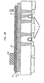
- a further interlevel dielectric layer formed of materials described herein, is deposited on top of the exposed layer 16 and over the resistor structure 20' and is planarized to form the structure shown in Figure 2(e) .
- via structures V1 may be formed using conventional techniques to electrically couple the resistor device 20' of the invention to a further metallization layer, e.g., M2.
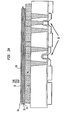
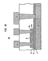
- the thin film resistor structure is sandwiched between two thin CDEL layers 50a, 50b.
- This entails process steps of sequentially depositing dielectric layers 14, 16, first CDEL layer 50a, the thin-film conductor layer 20 of material forming the thin-film resistor, a second CDEL layer 50b deposited atop the thin-film conductor layer 20 and, the final etch stop layer 25 deposited above the second CDEL layer 50b.
- the two thin CDEL layers 50a, 50b comprise deposited to a thickness of less than 100 ⁇ by atomic layer deposition (ALD) and preferably, to a thickness of about 50 ⁇ or less.
- ALD atomic layer deposition
- the CDEL layers 50a,b may comprise a thin layer of Aluminum, deposited to a thickness ranging between 10 ⁇ and 20 ⁇ and oxidized by an O 2 plasma or air oxidation.
- the CDEL layers 50a,b may comprise metal oxides such as Ta 2 O 5 , HfO 2 , ZrO 2 and the like.
- Sandwiched between the first and second CDEL layers 50a,b is the thin film resistor, comprising TaN, as described herein with respect to the first embodiment.
- the conductive metal 20 is a thin layer whose thickness is typically from about 300 ⁇ to about 700 ⁇ with a thickness of about 500 ⁇ nominally.
- the CDEL layers 50a,b are formed of a material that adheres well to the underlying thin film resistor material TaN and increases the current carrying capability of the resistor device as will be further described.
- the conductive metal 20 forming the thin-film resistor can be formed on the first CDEL layer 50a utilizing any deposition process including, for example, CVD, PECVD, sputtering, plating, evaporation, ALD and other like deposition processes.
- the second thin Current Density Enhancing Layer (CDEL) 50b is deposited on the conductive metal layer 20, and the etch stop layer 25 is deposited on CDEL layer 50b providing the structure shown in FIG. 3(a) .
- the thin-film resistor features are patterned using an applied lithographic mask (i.e., a resist layer not shown), and an etching step is performed to form the resistor device 20" such as shown in Figure 3(b) .
- an applied lithographic mask i.e., a resist layer not shown
- an etching step is performed to form the resistor device 20" such as shown in Figure 3(b) .
- This is accomplished by removing the layers 25, 50b, 20 and 50a outside of the defined mask perimeter and stopping on layer 16 as shown in Figure 3(b) .
- the formed photomask (resist) layer 120 is removed.
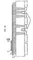
- a further interlevel dielectric layer 125 formed of materials described herein, is deposited on top of the exposed layer 16 and over the resistor structure 20" and is planarized to form the structure shown in Figure 3(c) .
- via structures V1 may be formed using conventional techniques to electrically couple the resistor device 20" of the invention to a further metallization layer, e.g
- Table 1 describes the resistance to shift for an example application of stress applied to an example resistor structure formed according to the present invention.
- the example resistor device structure is of a resistor size approximately 10 ⁇ m x 10 ⁇ m with an applied current density of 2mA/ ⁇ m of width.
- the stress is a high temperature stress of approximately 125° C applied for a period of 24 hours.
- I 0 is Current at Time 0 Hours - before current stress
- R 0 is resistance at Time 0 Hours - before current stress
- I 24 is the current after Time 24 Hours, i.e., the end of current stress
- R 24 is the device's resistance after time 24 Hours (end of current stress)
- %R 24 is shift in resistance after 24 hours of constant current stress at the above conditions.
- resistor formed according to a first embodiment of the invention where the resistor comprises a single CDEL layer of Al 2 O 3 layer of approximately 50 ⁇ , with a voltage impressed upon the resistor for a period of 24 hours at high temperature Table 1 reveals that a 5.4 % shift in resistance is exhibited as the initial resistance value, R 0 , at time zero is 66.93 ohms. This corresponds to an initial current I 0 , of about 20.6 mA with 1.38 V impressed. At 24 hours later, the current has decreased to about 19.56 mA corresponding to an increased resistance R 24 to about 70.55 ohms which corresponds to a per cent resistance shift of about 5.4 %.
- the resistor structure As the example one-sided 100 ⁇ CDEL layer resistor structure does not exhibit a marked increased resistance to shift as compared to an example one-sided 50 ⁇ CDEL layer resistor structure, it is preferred that the resistor structure be formed with a CDEL layer of 50 ⁇ or less.
- the resistor device of the present invention may be formed in front end of line processes, for example, formed on a substrate and coupled to other device regions including bipolar transistors and/or CMOS devices, such as FETs.
- the invention is useful in the field of semiconductor devices, and more particularly to thin-film resistors.
Landscapes
- Engineering & Computer Science (AREA)
- Power Engineering (AREA)
- Microelectronics & Electronic Packaging (AREA)
- Physics & Mathematics (AREA)
- Computer Hardware Design (AREA)
- Condensed Matter Physics & Semiconductors (AREA)
- General Physics & Mathematics (AREA)
- Electromagnetism (AREA)
- Semiconductor Integrated Circuits (AREA)
- Internal Circuitry In Semiconductor Integrated Circuit Devices (AREA)
- Non-Adjustable Resistors (AREA)
- Apparatuses And Processes For Manufacturing Resistors (AREA)
Claims (5)
- Dünnfilmwiderstand für eine Halbleiter-Schaltungsstruktur, welcher das Folgende umfasst:eine Dünnfilmschicht aus einem Leitermaterial (20), welches einen Widerstandswert aufweist, wobei die Dünnfilmschicht aus dem Leitermaterial (20) TaN umfasst; undeine Stromdichte-Erhöhungsschicht CDEL (Current Density Enhancing Layer, 50), welche oben auf der Dünnfilmschicht aus dem Leitermaterial (20) ausgebildet ist, wobei die Stromdichte-Erhöhungsschicht (50) dem Dünnfilmwiderstand ermöglicht, höhere Stromdichten mit einer verringerten Veränderung des Widerstandes zu übertragen;dadurch gekennzeichnet, dass die Stromdichte-Erhöhungsschicht Al2O3 umfasst und eine Dicke von weniger als 10 nm aufweist.
- Dünnfilmwiderstand nach Anspruch 1, welcher in einem Back-End-of-Line-Verfahren (BEOL-Verfahren) auf einer isolierenden Halbleiterstruktur gebildet wird.
- Dünnfilmwiderstand nach Anspruch 2, welcher über eine leitende Durchkontaktierungsstruktur elektrisch mit einer Metallebene einer Halbleiterschaltung verbunden ist.
- Dünnfilmwiderstand nach Anspruch 3, welcher ferner eine zusätzliche CDEL-Schicht (50) umfasst, die unter der Dünnfilmschicht aus dem Leitermaterial (20) ausgebildet ist, wobei die zusätzliche CDEL-Schicht Al2O3 umfasst und eine Dicke von weniger als 10 nm aufweist.
- Dünnfilmwiderstand nach Anspruch 1, welcher ferner eine isolierende Schicht umfasst, die oben auf dem Dünnfilmwiderstand ausgebildet ist.
Applications Claiming Priority (2)
| Application Number | Priority Date | Filing Date | Title |
|---|---|---|---|
| US10/906,365 US7271700B2 (en) | 2005-02-16 | 2005-02-16 | Thin film resistor with current density enhancing layer (CDEL) |
| PCT/US2006/004436 WO2006088709A2 (en) | 2005-02-16 | 2006-02-08 | Thin film resistors with current density enhancing layer (cdel) |
Publications (3)
| Publication Number | Publication Date |
|---|---|
| EP1849167A2 EP1849167A2 (de) | 2007-10-31 |
| EP1849167A4 EP1849167A4 (de) | 2010-06-09 |
| EP1849167B1 true EP1849167B1 (de) | 2011-12-21 |
Family
ID=36815104
Family Applications (1)
| Application Number | Title | Priority Date | Filing Date |
|---|---|---|---|
| EP06720491A Active EP1849167B1 (de) | 2005-02-16 | 2006-02-08 | Dünnfilmwiderstand mit einer Stromdichteverstärkungsschicht |
Country Status (7)
| Country | Link |
|---|---|
| US (1) | US7271700B2 (de) |
| EP (1) | EP1849167B1 (de) |
| JP (1) | JP5063365B2 (de) |
| CN (1) | CN101647075B (de) |
| AT (1) | ATE538480T1 (de) |
| TW (1) | TWI384497B (de) |
| WO (1) | WO2006088709A2 (de) |
Families Citing this family (24)
| Publication number | Priority date | Publication date | Assignee | Title |
|---|---|---|---|---|
| US7381981B2 (en) * | 2005-07-29 | 2008-06-03 | International Business Machines Corporation | Phase-change TaN resistor based triple-state/multi-state read only memory |
| US7749896B2 (en) * | 2005-08-23 | 2010-07-06 | Taiwan Semiconductor Manufacturing Co., Ltd. | Semiconductor device and method for forming the same |
| US8013394B2 (en) * | 2007-03-28 | 2011-09-06 | International Business Machines Corporation | Integrated circuit having resistor between BEOL interconnect and FEOL structure and related method |
| JP2011082195A (ja) * | 2008-02-04 | 2011-04-21 | Alps Electric Co Ltd | 半導体装置及びその製造方法 |
| US8426745B2 (en) * | 2009-11-30 | 2013-04-23 | Intersil Americas Inc. | Thin film resistor |
| US8169811B2 (en) * | 2010-07-13 | 2012-05-01 | Nxp B.V. | Non-volatile re-programmable memory device |
| US8455768B2 (en) | 2010-11-15 | 2013-06-04 | International Business Machines Corporation | Back-end-of-line planar resistor |
| US8680618B2 (en) * | 2011-10-17 | 2014-03-25 | Texas Instruments Incorporated | Structure and method for integrating front end SiCr resistors in HiK metal gate technologies |
| US8890222B2 (en) | 2012-02-03 | 2014-11-18 | Taiwan Semiconductor Manufacturing Company, Ltd. | Meander line resistor structure |
| CN103325844B (zh) * | 2012-03-19 | 2017-10-13 | 联华电子股份有限公司 | 薄膜电阻结构 |
| US8859386B2 (en) * | 2012-06-08 | 2014-10-14 | Taiwan Semiconductor Manufacturing Company, Ltd. | Semiconductor devices, methods of manufacture thereof, and methods of forming resistors |
| WO2014205634A1 (zh) * | 2013-06-24 | 2014-12-31 | 吉瑞高新科技股份有限公司 | 电子烟发热装置及电子烟 |
| US9502284B2 (en) * | 2013-12-31 | 2016-11-22 | Texas Instruments Incorporated | Metal thin film resistor and process |
| US9773779B2 (en) * | 2015-08-06 | 2017-09-26 | Taiwan Semiconductor Manufacturing Co., Ltd. | Semiconductor structure with resistor layer and method for forming the same |
| US10037990B2 (en) * | 2016-07-01 | 2018-07-31 | Taiwan Semiconductor Manufacturing Company, Ltd. | Method of manufacturing interconnect layer and semiconductor device which includes interconnect layer |
| US20180019298A1 (en) * | 2016-07-18 | 2018-01-18 | Raytheon Company | METHOD FOR FORMING PATTERNED TANTALUM NITRIDE (TaN) RESISTORS ON DIELECTRIC MATERIAL PASSIVATION LAYERS |
| US10211278B2 (en) * | 2017-07-11 | 2019-02-19 | Texas Instruments Incorporated | Device and method for a thin film resistor using a via retardation layer |
| US10763324B2 (en) * | 2017-07-25 | 2020-09-01 | Microchip Technology Incorporated | Systems and methods for forming a thin film resistor integrated in an integrated circuit device |
| US11756786B2 (en) | 2019-01-18 | 2023-09-12 | International Business Machines Corporation | Forming high carbon content flowable dielectric film with low processing damage |
| US11088024B2 (en) * | 2019-04-11 | 2021-08-10 | Microchip Technology Incorporated | Forming a thin film resistor (TFR) in an integrated circuit device |
| TW202125541A (zh) * | 2019-12-18 | 2021-07-01 | 光頡科技股份有限公司 | 薄膜電阻元件 |
| US11990257B2 (en) | 2020-02-27 | 2024-05-21 | Microchip Technology Incorporated | Thin film resistor (TFR) formed in an integrated circuit device using wet etching of a dielectric cap |
| US20210305155A1 (en) * | 2020-03-30 | 2021-09-30 | Qualcomm Incorporated | Via zero interconnect layer metal resistor integration |
| US20230063793A1 (en) * | 2021-08-26 | 2023-03-02 | Taiwan Semiconductor Manufacturing Company, Ltd. | Method (and related apparatus) for forming a resistor over a semiconductor substrate |
Family Cites Families (31)
| Publication number | Priority date | Publication date | Assignee | Title |
|---|---|---|---|---|
| US4166279A (en) * | 1977-12-30 | 1979-08-28 | International Business Machines Corporation | Electromigration resistance in gold thin film conductors |
| US4217570A (en) * | 1978-05-30 | 1980-08-12 | Tektronix, Inc. | Thin-film microcircuits adapted for laser trimming |
| US4232059A (en) | 1979-06-06 | 1980-11-04 | E-Systems, Inc. | Process of defining film patterns on microelectronic substrates by air abrading |
| US5356869A (en) * | 1987-09-28 | 1994-10-18 | Arch Development Corporation | Metal oxide superconducting powder comprised of flake-like single crystal particles |
| JPH03132022A (ja) | 1989-10-18 | 1991-06-05 | Hitachi Ltd | 半導体装置の製造方法およびその装置 |
| JPH04221850A (ja) * | 1990-12-20 | 1992-08-12 | Murata Mfg Co Ltd | 薄膜抵抗体 |
| US5679982A (en) | 1993-02-24 | 1997-10-21 | Intel Corporation | Barrier against metal diffusion |
| US5817574A (en) | 1993-12-29 | 1998-10-06 | Intel Corporation | Method of forming a high surface area interconnection structure |
| JP3510943B2 (ja) | 1995-10-27 | 2004-03-29 | 株式会社ルネサステクノロジ | 半導体装置の製造方法 |
| US6054659A (en) * | 1998-03-09 | 2000-04-25 | General Motors Corporation | Integrated electrostatically-actuated micromachined all-metal micro-relays |
| JP2001071499A (ja) | 1998-09-30 | 2001-03-21 | Canon Inc | インクジェット記録ヘッドとこれを備えるインクジェット装置およびインクジェット記録方法 |
| US6545359B1 (en) | 1998-12-18 | 2003-04-08 | Semiconductor Energy Laboratory Co., Ltd. | Wiring line and manufacture process thereof, and semiconductor device and manufacturing process thereof |
| US6703666B1 (en) * | 1999-07-14 | 2004-03-09 | Agere Systems Inc. | Thin film resistor device and a method of manufacture therefor |
| JP2001223334A (ja) * | 2000-02-09 | 2001-08-17 | Toshiba Corp | 半導体装置製造方法および半導体装置 |
| JP3715502B2 (ja) * | 2000-03-14 | 2005-11-09 | 株式会社東芝 | 半導体装置及びその製造方法 |
| TW471163B (en) * | 2000-08-17 | 2002-01-01 | United Microelectronics Corp | Manufacturing method and structure of thin film resistor having a high resistance value |
| US7214295B2 (en) * | 2001-04-09 | 2007-05-08 | Vishay Dale Electronics, Inc. | Method for tantalum pentoxide moisture barrier in film resistors |
| US6599827B1 (en) | 2001-05-02 | 2003-07-29 | Advanced Micro Devices, Inc. | Methods of forming capped copper interconnects with improved electromigration resistance |
| US6432822B1 (en) | 2001-05-02 | 2002-08-13 | Advanced Micro Devices, Inc. | Method of improving electromigration resistance of capped Cu |
| US6534374B2 (en) | 2001-06-07 | 2003-03-18 | Institute Of Microelectronics | Single damascene method for RF IC passive component integration in copper interconnect process |
| TW495959B (en) * | 2001-06-26 | 2002-07-21 | Taiwan Semiconductor Mfg | Highly precise semiconductor thin film resistor and the manufacturing method thereof |
| JP4088052B2 (ja) * | 2001-07-17 | 2008-05-21 | 株式会社東芝 | 半導体装置の製造方法 |
| US6933186B2 (en) | 2001-09-21 | 2005-08-23 | International Business Machines Corporation | Method for BEOL resistor tolerance improvement using anodic oxidation |
| JP3948263B2 (ja) * | 2001-11-28 | 2007-07-25 | ソニー株式会社 | 半導体装置の製造方法 |
| JP2003243520A (ja) | 2002-02-19 | 2003-08-29 | Alps Electric Co Ltd | 半導体装置及び半導体装置の製造方法 |
| JP3969192B2 (ja) | 2002-05-30 | 2007-09-05 | 株式会社デンソー | 多層配線基板の製造方法 |
| DE10224167B4 (de) | 2002-05-31 | 2007-01-25 | Advanced Micro Devices, Inc., Sunnyvale | Verfahren zur Herstellung einer Kupferleitung mit erhöhter Widerstandsfähigkeit gegen Elektromigration in einem Halbleiterelement |
| US6730573B1 (en) * | 2002-11-01 | 2004-05-04 | Chartered Semiconductor Manufacturing Ltd. | MIM and metal resistor formation at CU beol using only one extra mask |
| US6872655B2 (en) | 2003-02-04 | 2005-03-29 | Texas Instruments Incorporated | Method of forming an integrated circuit thin film resistor |
| US6858527B2 (en) | 2003-04-14 | 2005-02-22 | Intel Corporation | Method to increase electromigration resistance of copper using self-assembled organic thiolate monolayers |
| TWI224820B (en) * | 2003-10-03 | 2004-12-01 | Mosel Vitelic Inc | Method for manufacturing trench-typed MOSFET |
-
2005
- 2005-02-16 US US10/906,365 patent/US7271700B2/en active Active
-
2006
- 2006-02-07 TW TW095104024A patent/TWI384497B/zh active
- 2006-02-08 AT AT06720491T patent/ATE538480T1/de active
- 2006-02-08 JP JP2007556200A patent/JP5063365B2/ja not_active Expired - Fee Related
- 2006-02-08 CN CN200680004973.6A patent/CN101647075B/zh active Active
- 2006-02-08 WO PCT/US2006/004436 patent/WO2006088709A2/en active Application Filing
- 2006-02-08 EP EP06720491A patent/EP1849167B1/de active Active
Also Published As
| Publication number | Publication date |
|---|---|
| WO2006088709A3 (en) | 2009-04-30 |
| WO2006088709A2 (en) | 2006-08-24 |
| JP2008530820A (ja) | 2008-08-07 |
| US7271700B2 (en) | 2007-09-18 |
| CN101647075A (zh) | 2010-02-10 |
| JP5063365B2 (ja) | 2012-10-31 |
| EP1849167A4 (de) | 2010-06-09 |
| ATE538480T1 (de) | 2012-01-15 |
| TWI384497B (zh) | 2013-02-01 |
| EP1849167A2 (de) | 2007-10-31 |
| CN101647075B (zh) | 2011-08-31 |
| TW200643992A (en) | 2006-12-16 |
| US20060181388A1 (en) | 2006-08-17 |
Similar Documents
| Publication | Publication Date | Title |
|---|---|---|
| EP1849167B1 (de) | Dünnfilmwiderstand mit einer Stromdichteverstärkungsschicht | |
| US6890810B2 (en) | Method of fabrication of thin film resistor with zero TCR | |
| US8212649B2 (en) | Semiconductor device and manufacturing method of the same | |
| JP4906722B2 (ja) | 高性能cmosのためのfeol/meol金属抵抗器 | |
| US7807540B2 (en) | Back end thin film capacitor having plates at thin film resistor and first metallization layer levels | |
| US7964919B2 (en) | Thin film resistors integrated at two different metal single die | |
| US6921962B1 (en) | Integrated circuit having a thin film resistor located within a multilevel dielectric between an upper and lower metal interconnect layer | |
| US7768127B2 (en) | Semiconductor device including multi-layered interconnection and method of manufacturing the device | |
| KR20040016388A (ko) | 응력 조정 캡층을 포함한 상호 접속 구조 | |
| US20070176295A1 (en) | Contact via scheme with staggered vias | |
| US11637100B2 (en) | Semiconductor device having capacitor and resistor and a method of forming the same | |
| US6737326B2 (en) | Method of integrating a thin film resistor in a multi-level metal tungsten-plug interconnect | |
| US7202533B1 (en) | Thin film resistors integrated at a single metal interconnect level of die | |
| US20010046771A1 (en) | Thin film resistor having improved temperature independence and a method of engineering the TCR of the thin film resistor | |
| US20230037025A1 (en) | Method of manufacturing a semiconductor device and a semiconductor device | |
| KR101100762B1 (ko) | 엠아이엠 캐패시터 및 그 제조 방법 | |
| TW202415277A (zh) | 半導體結構及其製造方法 | |
| EP1168379A2 (de) | Verfahren zur Herstellung eines Dünnschichtwiderstandes mit vorbestimmtem Temperaturkoeffizient | |
| CN116936523A (zh) | 半导体器件 |
Legal Events
| Date | Code | Title | Description |
|---|---|---|---|
| PUAI | Public reference made under article 153(3) epc to a published international application that has entered the european phase |
Free format text: ORIGINAL CODE: 0009012 |
|
| 17P | Request for examination filed |
Effective date: 20070821 |
|
| AK | Designated contracting states |
Kind code of ref document: A2 Designated state(s): AT BE BG CH CY CZ DE DK EE ES FI FR GB GR HU IE IS IT LI LT LU LV MC NL PL PT RO SE SI SK TR |
|
| AX | Request for extension of the european patent |
Extension state: AL BA HR MK YU |
|
| DAX | Request for extension of the european patent (deleted) | ||
| R17D | Deferred search report published (corrected) |
Effective date: 20090430 |
|
| A4 | Supplementary search report drawn up and despatched |
Effective date: 20100511 |
|
| RIC1 | Information provided on ipc code assigned before grant |
Ipc: H01L 23/522 20060101ALN20100505BHEP Ipc: H01L 27/06 20060101ALI20100505BHEP Ipc: H01C 1/012 20060101AFI20060830BHEP Ipc: H01L 21/02 20060101ALI20100505BHEP |
|
| 17Q | First examination report despatched |
Effective date: 20110214 |
|
| RIC1 | Information provided on ipc code assigned before grant |
Ipc: H01L 23/522 20060101ALN20110729BHEP Ipc: H01C 7/00 20060101ALI20110729BHEP Ipc: H01L 21/02 20060101ALI20110729BHEP Ipc: H01C 1/012 20060101AFI20110729BHEP Ipc: H01L 27/06 20060101ALI20110729BHEP |
|
| RTI1 | Title (correction) |
Free format text: THIN-FILM RESISTOR WITH A CURRENT-DENSITY-ENHANCING LAYER |
|
| GRAP | Despatch of communication of intention to grant a patent |
Free format text: ORIGINAL CODE: EPIDOSNIGR1 |
|
| GRAS | Grant fee paid |
Free format text: ORIGINAL CODE: EPIDOSNIGR3 |
|
| GRAA | (expected) grant |
Free format text: ORIGINAL CODE: 0009210 |
|
| AK | Designated contracting states |
Kind code of ref document: B1 Designated state(s): AT BE BG CH CY CZ DE DK EE ES FI FR GB GR HU IE IS IT LI LT LU LV MC NL PL PT RO SE SI SK TR |
|
| REG | Reference to a national code |
Ref country code: GB Ref legal event code: FG4D |
|
| REG | Reference to a national code |
Ref country code: CH Ref legal event code: EP |
|
| REG | Reference to a national code |
Ref country code: DE Ref legal event code: R084 Ref document number: 602006026517 Country of ref document: DE |
|
| REG | Reference to a national code |
Ref country code: AT Ref legal event code: REF Ref document number: 538480 Country of ref document: AT Kind code of ref document: T Effective date: 20120115 |
|
| REG | Reference to a national code |
Ref country code: DE Ref legal event code: R081 Ref document number: 602006026517 Country of ref document: DE Owner name: GLOBALFOUNDRIES INC., KY Free format text: FORMER OWNER: INTERNATIONAL BUSINESS MACHINES CORPORATION, ARMONK, N.Y., US |
|
| REG | Reference to a national code |
Ref country code: IE Ref legal event code: FG4D |
|
| REG | Reference to a national code |
Ref country code: GB Ref legal event code: 746 Effective date: 20120130 |
|
| REG | Reference to a national code |
Ref country code: DE Ref legal event code: R096 Ref document number: 602006026517 Country of ref document: DE Effective date: 20120308 Ref country code: DE Ref legal event code: R084 Ref document number: 602006026517 Country of ref document: DE Effective date: 20120110 |
|
| REG | Reference to a national code |
Ref country code: NL Ref legal event code: VDEP Effective date: 20111221 |
|
| PG25 | Lapsed in a contracting state [announced via postgrant information from national office to epo] |
Ref country code: LT Free format text: LAPSE BECAUSE OF FAILURE TO SUBMIT A TRANSLATION OF THE DESCRIPTION OR TO PAY THE FEE WITHIN THE PRESCRIBED TIME-LIMIT Effective date: 20111221 |
|
| LTIE | Lt: invalidation of european patent or patent extension |
Effective date: 20111221 |
|
| PG25 | Lapsed in a contracting state [announced via postgrant information from national office to epo] |
Ref country code: SI Free format text: LAPSE BECAUSE OF FAILURE TO SUBMIT A TRANSLATION OF THE DESCRIPTION OR TO PAY THE FEE WITHIN THE PRESCRIBED TIME-LIMIT Effective date: 20111221 Ref country code: NL Free format text: LAPSE BECAUSE OF FAILURE TO SUBMIT A TRANSLATION OF THE DESCRIPTION OR TO PAY THE FEE WITHIN THE PRESCRIBED TIME-LIMIT Effective date: 20111221 Ref country code: LV Free format text: LAPSE BECAUSE OF FAILURE TO SUBMIT A TRANSLATION OF THE DESCRIPTION OR TO PAY THE FEE WITHIN THE PRESCRIBED TIME-LIMIT Effective date: 20111221 Ref country code: SE Free format text: LAPSE BECAUSE OF FAILURE TO SUBMIT A TRANSLATION OF THE DESCRIPTION OR TO PAY THE FEE WITHIN THE PRESCRIBED TIME-LIMIT Effective date: 20111221 Ref country code: GR Free format text: LAPSE BECAUSE OF FAILURE TO SUBMIT A TRANSLATION OF THE DESCRIPTION OR TO PAY THE FEE WITHIN THE PRESCRIBED TIME-LIMIT Effective date: 20120322 |
|
| PG25 | Lapsed in a contracting state [announced via postgrant information from national office to epo] |
Ref country code: CY Free format text: LAPSE BECAUSE OF FAILURE TO SUBMIT A TRANSLATION OF THE DESCRIPTION OR TO PAY THE FEE WITHIN THE PRESCRIBED TIME-LIMIT Effective date: 20111221 Ref country code: BE Free format text: LAPSE BECAUSE OF FAILURE TO SUBMIT A TRANSLATION OF THE DESCRIPTION OR TO PAY THE FEE WITHIN THE PRESCRIBED TIME-LIMIT Effective date: 20111221 |
|
| PG25 | Lapsed in a contracting state [announced via postgrant information from national office to epo] |
Ref country code: EE Free format text: LAPSE BECAUSE OF FAILURE TO SUBMIT A TRANSLATION OF THE DESCRIPTION OR TO PAY THE FEE WITHIN THE PRESCRIBED TIME-LIMIT Effective date: 20111221 Ref country code: CZ Free format text: LAPSE BECAUSE OF FAILURE TO SUBMIT A TRANSLATION OF THE DESCRIPTION OR TO PAY THE FEE WITHIN THE PRESCRIBED TIME-LIMIT Effective date: 20111221 Ref country code: BG Free format text: LAPSE BECAUSE OF FAILURE TO SUBMIT A TRANSLATION OF THE DESCRIPTION OR TO PAY THE FEE WITHIN THE PRESCRIBED TIME-LIMIT Effective date: 20120321 Ref country code: SK Free format text: LAPSE BECAUSE OF FAILURE TO SUBMIT A TRANSLATION OF THE DESCRIPTION OR TO PAY THE FEE WITHIN THE PRESCRIBED TIME-LIMIT Effective date: 20111221 Ref country code: IS Free format text: LAPSE BECAUSE OF FAILURE TO SUBMIT A TRANSLATION OF THE DESCRIPTION OR TO PAY THE FEE WITHIN THE PRESCRIBED TIME-LIMIT Effective date: 20120421 |
|
| PG25 | Lapsed in a contracting state [announced via postgrant information from national office to epo] |
Ref country code: PT Free format text: LAPSE BECAUSE OF FAILURE TO SUBMIT A TRANSLATION OF THE DESCRIPTION OR TO PAY THE FEE WITHIN THE PRESCRIBED TIME-LIMIT Effective date: 20120423 Ref country code: RO Free format text: LAPSE BECAUSE OF FAILURE TO SUBMIT A TRANSLATION OF THE DESCRIPTION OR TO PAY THE FEE WITHIN THE PRESCRIBED TIME-LIMIT Effective date: 20111221 Ref country code: PL Free format text: LAPSE BECAUSE OF FAILURE TO SUBMIT A TRANSLATION OF THE DESCRIPTION OR TO PAY THE FEE WITHIN THE PRESCRIBED TIME-LIMIT Effective date: 20111221 |
|
| REG | Reference to a national code |
Ref country code: AT Ref legal event code: MK05 Ref document number: 538480 Country of ref document: AT Kind code of ref document: T Effective date: 20111221 |
|
| PG25 | Lapsed in a contracting state [announced via postgrant information from national office to epo] |
Ref country code: MC Free format text: LAPSE BECAUSE OF NON-PAYMENT OF DUE FEES Effective date: 20120229 |
|
| REG | Reference to a national code |
Ref country code: CH Ref legal event code: PL |
|
| PLBE | No opposition filed within time limit |
Free format text: ORIGINAL CODE: 0009261 |
|
| STAA | Information on the status of an ep patent application or granted ep patent |
Free format text: STATUS: NO OPPOSITION FILED WITHIN TIME LIMIT |
|
| PG25 | Lapsed in a contracting state [announced via postgrant information from national office to epo] |
Ref country code: CH Free format text: LAPSE BECAUSE OF NON-PAYMENT OF DUE FEES Effective date: 20120229 Ref country code: LI Free format text: LAPSE BECAUSE OF NON-PAYMENT OF DUE FEES Effective date: 20120229 Ref country code: DK Free format text: LAPSE BECAUSE OF FAILURE TO SUBMIT A TRANSLATION OF THE DESCRIPTION OR TO PAY THE FEE WITHIN THE PRESCRIBED TIME-LIMIT Effective date: 20111221 |
|
| REG | Reference to a national code |
Ref country code: IE Ref legal event code: MM4A |
|
| REG | Reference to a national code |
Ref country code: FR Ref legal event code: ST Effective date: 20121031 |
|
| 26N | No opposition filed |
Effective date: 20120924 |
|
| PG25 | Lapsed in a contracting state [announced via postgrant information from national office to epo] |
Ref country code: IT Free format text: LAPSE BECAUSE OF FAILURE TO SUBMIT A TRANSLATION OF THE DESCRIPTION OR TO PAY THE FEE WITHIN THE PRESCRIBED TIME-LIMIT Effective date: 20111221 |
|
| REG | Reference to a national code |
Ref country code: DE Ref legal event code: R097 Ref document number: 602006026517 Country of ref document: DE Effective date: 20120924 |
|
| PG25 | Lapsed in a contracting state [announced via postgrant information from national office to epo] |
Ref country code: FR Free format text: LAPSE BECAUSE OF NON-PAYMENT OF DUE FEES Effective date: 20120229 Ref country code: IE Free format text: LAPSE BECAUSE OF NON-PAYMENT OF DUE FEES Effective date: 20120208 Ref country code: AT Free format text: LAPSE BECAUSE OF FAILURE TO SUBMIT A TRANSLATION OF THE DESCRIPTION OR TO PAY THE FEE WITHIN THE PRESCRIBED TIME-LIMIT Effective date: 20111221 |
|
| PG25 | Lapsed in a contracting state [announced via postgrant information from national office to epo] |
Ref country code: ES Free format text: LAPSE BECAUSE OF FAILURE TO SUBMIT A TRANSLATION OF THE DESCRIPTION OR TO PAY THE FEE WITHIN THE PRESCRIBED TIME-LIMIT Effective date: 20120401 |
|
| PG25 | Lapsed in a contracting state [announced via postgrant information from national office to epo] |
Ref country code: FI Free format text: LAPSE BECAUSE OF FAILURE TO SUBMIT A TRANSLATION OF THE DESCRIPTION OR TO PAY THE FEE WITHIN THE PRESCRIBED TIME-LIMIT Effective date: 20111221 |
|
| PG25 | Lapsed in a contracting state [announced via postgrant information from national office to epo] |
Ref country code: TR Free format text: LAPSE BECAUSE OF FAILURE TO SUBMIT A TRANSLATION OF THE DESCRIPTION OR TO PAY THE FEE WITHIN THE PRESCRIBED TIME-LIMIT Effective date: 20111221 |
|
| PG25 | Lapsed in a contracting state [announced via postgrant information from national office to epo] |
Ref country code: LU Free format text: LAPSE BECAUSE OF NON-PAYMENT OF DUE FEES Effective date: 20120208 |
|
| PG25 | Lapsed in a contracting state [announced via postgrant information from national office to epo] |
Ref country code: HU Free format text: LAPSE BECAUSE OF FAILURE TO SUBMIT A TRANSLATION OF THE DESCRIPTION OR TO PAY THE FEE WITHIN THE PRESCRIBED TIME-LIMIT Effective date: 20060208 |
|
| PGFP | Annual fee paid to national office [announced via postgrant information from national office to epo] |
Ref country code: GB Payment date: 20150226 Year of fee payment: 10 |
|
| REG | Reference to a national code |
Ref country code: DE Ref legal event code: R081 Ref document number: 602006026517 Country of ref document: DE Owner name: GLOBALFOUNDRIES U.S. INC., SANTA CLARA, US Free format text: FORMER OWNER: INTERNATIONAL BUSINESS MACHINES CORPORATION, ARMONK, N.Y., US Ref country code: DE Ref legal event code: R081 Ref document number: 602006026517 Country of ref document: DE Owner name: GLOBALFOUNDRIES INC., KY Free format text: FORMER OWNER: INTERNATIONAL BUSINESS MACHINES CORPORATION, ARMONK, N.Y., US |
|
| REG | Reference to a national code |
Ref country code: DE Ref legal event code: R081 Ref document number: 602006026517 Country of ref document: DE Owner name: GLOBALFOUNDRIES U.S. INC., SANTA CLARA, US Free format text: FORMER OWNER: GLOBALFOUNDRIES US 2 LLC (N.D.GES.DES STAATES DELAWARE), HOPEWELL JUNCTION, N.Y., US Ref country code: DE Ref legal event code: R082 Ref document number: 602006026517 Country of ref document: DE Representative=s name: GRUENECKER PATENT- UND RECHTSANWAELTE PARTG MB, DE Ref country code: DE Ref legal event code: R082 Ref document number: 602006026517 Country of ref document: DE Representative=s name: RICHARDT PATENTANWAELTE PARTG MBB, DE Ref country code: DE Ref legal event code: R081 Ref document number: 602006026517 Country of ref document: DE Owner name: GLOBALFOUNDRIES INC., KY Free format text: FORMER OWNER: GLOBALFOUNDRIES US 2 LLC (N.D.GES.DES STAATES DELAWARE), HOPEWELL JUNCTION, N.Y., US |
|
| GBPC | Gb: european patent ceased through non-payment of renewal fee |
Effective date: 20160208 |
|
| PG25 | Lapsed in a contracting state [announced via postgrant information from national office to epo] |
Ref country code: GB Free format text: LAPSE BECAUSE OF NON-PAYMENT OF DUE FEES Effective date: 20160208 |
|
| REG | Reference to a national code |
Ref country code: DE Ref legal event code: R082 Ref document number: 602006026517 Country of ref document: DE Representative=s name: GRUENECKER PATENT- UND RECHTSANWAELTE PARTG MB, DE Ref country code: DE Ref legal event code: R081 Ref document number: 602006026517 Country of ref document: DE Owner name: GLOBALFOUNDRIES U.S. INC., SANTA CLARA, US Free format text: FORMER OWNER: GLOBALFOUNDRIES INC., GRAND CAYMAN, KY |
|
| P01 | Opt-out of the competence of the unified patent court (upc) registered |
Effective date: 20230412 |
|
| PGFP | Annual fee paid to national office [announced via postgrant information from national office to epo] |
Ref country code: DE Payment date: 20231212 Year of fee payment: 19 |