EP1835339A1 - Fabrication process by LIGA type technology, of a monolayer or multilayer metallic structure, and structure obtained therewith - Google Patents
Fabrication process by LIGA type technology, of a monolayer or multilayer metallic structure, and structure obtained therewith Download PDFInfo
- Publication number
- EP1835339A1 EP1835339A1 EP06405114A EP06405114A EP1835339A1 EP 1835339 A1 EP1835339 A1 EP 1835339A1 EP 06405114 A EP06405114 A EP 06405114A EP 06405114 A EP06405114 A EP 06405114A EP 1835339 A1 EP1835339 A1 EP 1835339A1
- Authority
- EP
- European Patent Office
- Prior art keywords
- photoresist
- substrate
- layer
- metal
- metal structure
- Prior art date
- Legal status (The legal status is an assumption and is not a legal conclusion. Google has not performed a legal analysis and makes no representation as to the accuracy of the status listed.)
- Granted
Links
Images


Classifications
-
- C—CHEMISTRY; METALLURGY
- C25—ELECTROLYTIC OR ELECTROPHORETIC PROCESSES; APPARATUS THEREFOR
- C25D—PROCESSES FOR THE ELECTROLYTIC OR ELECTROPHORETIC PRODUCTION OF COATINGS; ELECTROFORMING; APPARATUS THEREFOR
- C25D1/00—Electroforming
- C25D1/003—3D structures, e.g. superposed patterned layers
-
- B—PERFORMING OPERATIONS; TRANSPORTING
- B81—MICROSTRUCTURAL TECHNOLOGY
- B81C—PROCESSES OR APPARATUS SPECIALLY ADAPTED FOR THE MANUFACTURE OR TREATMENT OF MICROSTRUCTURAL DEVICES OR SYSTEMS
- B81C99/00—Subject matter not provided for in other groups of this subclass
- B81C99/0075—Manufacture of substrate-free structures
- B81C99/0085—Manufacture of substrate-free structures using moulds and master templates, e.g. for hot-embossing
-
- C—CHEMISTRY; METALLURGY
- C25—ELECTROLYTIC OR ELECTROPHORETIC PROCESSES; APPARATUS THEREFOR
- C25D—PROCESSES FOR THE ELECTROLYTIC OR ELECTROPHORETIC PRODUCTION OF COATINGS; ELECTROFORMING; APPARATUS THEREFOR
- C25D1/00—Electroforming
- C25D1/20—Separation of the formed objects from the electrodes with no destruction of said electrodes
-
- G—PHYSICS
- G03—PHOTOGRAPHY; CINEMATOGRAPHY; ANALOGOUS TECHNIQUES USING WAVES OTHER THAN OPTICAL WAVES; ELECTROGRAPHY; HOLOGRAPHY
- G03F—PHOTOMECHANICAL PRODUCTION OF TEXTURED OR PATTERNED SURFACES, e.g. FOR PRINTING, FOR PROCESSING OF SEMICONDUCTOR DEVICES; MATERIALS THEREFOR; ORIGINALS THEREFOR; APPARATUS SPECIALLY ADAPTED THEREFOR
- G03F7/00—Photomechanical, e.g. photolithographic, production of textured or patterned surfaces, e.g. printing surfaces; Materials therefor, e.g. comprising photoresists; Apparatus specially adapted therefor
-
- B—PERFORMING OPERATIONS; TRANSPORTING
- B81—MICROSTRUCTURAL TECHNOLOGY
- B81B—MICROSTRUCTURAL DEVICES OR SYSTEMS, e.g. MICROMECHANICAL DEVICES
- B81B2201/00—Specific applications of microelectromechanical systems
- B81B2201/03—Microengines and actuators
- B81B2201/035—Microgears
-
- B—PERFORMING OPERATIONS; TRANSPORTING
- B81—MICROSTRUCTURAL TECHNOLOGY
- B81C—PROCESSES OR APPARATUS SPECIALLY ADAPTED FOR THE MANUFACTURE OR TREATMENT OF MICROSTRUCTURAL DEVICES OR SYSTEMS
- B81C2201/00—Manufacture or treatment of microstructural devices or systems
- B81C2201/03—Processes for manufacturing substrate-free structures
- B81C2201/032—LIGA process
Landscapes
- Chemical & Material Sciences (AREA)
- Engineering & Computer Science (AREA)
- Materials Engineering (AREA)
- Chemical Kinetics & Catalysis (AREA)
- Electrochemistry (AREA)
- Metallurgy (AREA)
- Organic Chemistry (AREA)
- General Physics & Mathematics (AREA)
- Physics & Mathematics (AREA)
- Crystallography & Structural Chemistry (AREA)
- Manufacturing & Machinery (AREA)
- Microelectronics & Electronic Packaging (AREA)
- Micromachines (AREA)
- Moulds For Moulding Plastics Or The Like (AREA)
- Laminated Bodies (AREA)
Abstract
Description
La présente invention concerne un nouveau procédé de fabrication par une technologie de type LIGA d'une structure métallique monocouche ou multicouche, ainsi qu'une nouvelle structure métallique monocouche ou multicouche susceptible d'être obtenue par ce procédé.The present invention relates to a new method of manufacture by a LIGA type of technology of a monolayer or multilayer metal structure, as well as a new single-layer or multilayer metal structure that can be obtained by this method.
DGC Mitteilungen No. 104, 2005, mentionne l'utilisation de la technologie LIGA (
Le procédé utilisé pour la fabrication de structures métalliques monocouches comprend les étapes suivantes :
- créer sur une plaquette support en silicium une couche métallique sacrificielle et une couche d'ensemencement pour l'électrodéposition,
- étaler par dépôt à la tournette (spin-coating) une couche de polyimide photosensible,
- effectuer à travers un masque correspondant à l'empreinte désirée une illumination UV,
- développer en dissolvant les parties non irradiées de façon à obtenir un moule en polyimide,
- déposer galvaniquement du nickel ou du cuivre dans la partie ouverte du moule jusqu'à la hauteur de celui-ci, et
- éliminer la couche sacrificielle et séparer de la plaquette support la structure métallique obtenue par électroformage, et enlever le moule en polyimide.
- create on a silicon support wafer a sacrificial metal layer and a seeding layer for electroplating,
- spin-coating a layer of photosensitive polyimide,
- perform through a mask corresponding to the desired imprint a UV illumination,
- develop by dissolving the non-irradiated parts to obtain a polyimide mold,
- galvanically depositing nickel or copper in the open part of the mold up to the height thereof, and
- removing the sacrificial layer and separating the metal structure obtained by electroforming from the support plate, and removing the polyimide mold.
Ce document décrit la fabrication à l'aide de ce procédé de structures métalliques monocouches telles des engrenages en cuivre ou en nickel (cf. A) et B) pp. 89-91 et Figs. 3-7).This document describes the manufacture by means of this method of monolayer metal structures such as copper or nickel gears (see A) and B) pp. 89-91 and Figs. 3-7).
Frazier et al. divulgue aussi un procédé de fabrication de structures métalliques bicouches comportant les étapes suivantes :
- créer sur une plaquette support en silicium une couche métallique sacrificielle et une couche d'ensemencement pour l'électrodéposition,
- étaler par dépôt à la tournette (spin-coating) une couche de polyimide photosensible,
- effectuer à travers un masque correspondant à l'empreinte désirée une illumination aux rayons ultraviolets,
- développer en dissolvant les parties non irradiées de façon à obtenir un moule en polyimide,
- déposer galvaniquement du nickel dans la partie ouverte du moule jusqu'à hauteur de celui-ci de façon à obtenir une surface supérieure sensiblement plane,
- déposer par vaporisation sous vide une couche fine de chrome,
- déposer sur cette couche fine de chrome une couche de polyimide photosensible par dépôt à la tournette (spin-coating), et enlever la couche fine de chrome avec une solution d'acide chlorhydrique,
- effectuer une illumination UV à travers un nouveau masque correspondant à l'empreinte désirée, développer en dissolvant les parties non irradiées de façon à obtenir un nouveau moule en polyimide, et déposer galvaniquement du nickel dans la partie ouverte du moule, et
- éliminer la couche sacrificielle, séparer la structure métallique obtenue par électrodéposition de la plaquette support et éliminer le moule en polyimide.
- create on a silicon support wafer a sacrificial metal layer and a seeding layer for electroplating,
- spin-coating a layer of photosensitive polyimide,
- perform through a mask corresponding to the desired imprint ultraviolet illumination,
- develop by dissolving the non-irradiated parts to obtain a polyimide mold,
- galvanically depositing nickel in the open portion of the mold to a height thereof so as to obtain a substantially flat upper surface,
- vacuum vaporize a thin layer of chromium,
- deposit on this thin layer of chromium a layer of photosensitive polyimide by spin-coating, and remove the thin layer of chromium with a solution of hydrochloric acid,
- perform a UV illumination through a new mask corresponding to the desired imprint, develop by dissolving the non-irradiated parts so as to obtain a new polyimide mold, and galvanically deposit nickel in the open part of the mold, and
- remove the sacrificial layer, separate the metal structure obtained by electroplating the support plate and remove the polyimide mold.
Ce document décrit l'utilisation de ce procédé pour fabriquer une plaque métallique surmontée d'une protubérance de forme générale parallélépipédique (V. et Fig.9 page 92), la deuxième couche étant entièrement superposée sur la première couche de surface plus grande.This document describes the use of this method to manufacture a metal plate surmounted by a protuberance of parallelepipedal general shape (V. and Fig.9 page 92), the second layer being entirely superimposed on the first larger surface layer.
Les procédés décrits par Frazier et al. ne permettent pas d'effectuer d'opération d'usinage des structures fabriquées avant que celles-ci ne soient détachées de la plaquette-support en silicium. En effet celle-ci est trop fragile pour résister aux efforts mécaniques générés par un usinage. Si une opération d'usinage est nécessaire, elle nécessite le positionnement précis et l'immobilisation de chaque structure métallique fabriquée, ce qui rend la fabrication compliquée et difficile à mettre en oeuvre.The methods described by Frazier et al. do not allow to perform machining operation of the structures manufactured before they are detached from the silicon support plate. Indeed it is too fragile to resist the mechanical forces generated by machining. If a machining operation is necessary, it requires the precise positioning and immobilization of each fabricated metal structure, which makes the manufacture complicated and difficult to implement.
- 1) ou un microcapteur de flux thermique tricouche (Exemple 3). Ce procédé est proche de celui décrit par Frazier et al. et présente aussi les inconvénients exposés ci-dessus.
- 1) or a three-layer heat flux microsensor (Example 3). This method is close to that described by Frazier et al. and also has the disadvantages set forth above.
Le problème ou but de l'invention est de trouver un procédé de fabrication d'une structure métallique qui ne présente pas ces inconvénients.The problem or object of the invention is to find a method of manufacturing a metal structure that does not have these disadvantages.
Ce problème est résolu par l'invention telle que définie par les revendications.This problem is solved by the invention as defined by the claims.
La Demanderesse a en effet découvert que l'utilisation d'un substrat métallique massif à la place d'une plaquette support en silicium couverte d'une couche métallique sacrificielle et d'une couche d'ensemencement, permet d'usiner in situ la structure à l'issue de l'étape d'électroformage avant le détachage du substrat. On peut ainsi lors de la fabrication d'un grand nombre de structures (ou pièces) sur un même substrat usiner collectivement ces structures précisément positionnées et immobilisées sur celui-ci. L'étape supplémentaire de positionnement et d'immobilisation de chaque structure après détachage du substrat en vue d'un usinage ultérieur n'est donc plus nécessaire.The Applicant has in fact discovered that the use of a solid metal substrate in place of a silicon support wafer covered with a sacrificial metal layer and a seeding layer makes it possible to machine the structure in situ. at the end of the electroforming step before detaching the substrate. It is thus possible during the manufacture of a large number of structures (or parts) on the same substrate collectively machining these precisely positioned structures and immobilized thereon. The additional step of positioning and immobilization of each structure after detaching the substrate for subsequent machining is no longer necessary.
De plus, dans le cas de la fabrication de structures métalliques multicouches, l'utilisation d'un support métallique massif permet une mise à niveau par usinage (abrasion et polissage) à la fin de chaque étape d'électrodéposition de façon à obtenir une surface supérieure plane. Ceci a pour effet d'améliorer la qualité de la structure métallique multicouche obtenue car le dépôt électrolytique ultérieur s'effectue de façon plus régulière sur une surface polie que sur une surface présentant des irrégularités.In addition, in the case of the manufacture of multilayer metal structures, the use of a solid metal support allows a leveling by machining (abrasion and polishing) at the end of each electrodeposition step so as to obtain a surface upper plane. This has the effect of improving the quality of the multilayer metal structure obtained because the subsequent electrolytic deposition is performed more evenly on a polished surface than on a surface with irregularities.
L'invention concerne ainsi un procédé de fabrication par une technologie de type LIGA d'une structure métallique monocouche ou multicouche, dans lequel on étale une couche de photorésist sur un substrat, on crée par irradiation ou bombardement ionique un moule de photorésist, on dépose galvaniquement un métal ou un alliage dans ce moule, on détache la structure métallique du substrat et on sépare le photorésist, caractérisé en ce que le substrat est un substrat métallique massif. L'irradiation dans un tel procédé de type LIGA peut être une irradiation aux rayons X ou une irradiation aux rayons UV, par illumination en mode normal à travers un masque, par illumination en mode laser pour créer un réseau de zones polymérisées ou par ablation par laser.The invention thus relates to a method of manufacturing by a LIGA type of technology a monolayer or multilayer metal structure, in which a layer of photoresist is spread on a substrate, is created by irradiation or ion bombardment a photoresist mold, is deposited galvanically a metal or an alloy in this mold, the metal structure is detached from the substrate and the photoresist, characterized in that the substrate is a solid metal substrate. Irradiation in such a LIGA type process can be X-ray irradiation or UV irradiation, normal mode illumination through a mask, laser mode illumination to create a network of polymerized zones or ablation by laser.
De préférence la technologie de type LIGA est une technologie de type LIGA-UV, c'est à dire une technologie de type LIGA utilisant une irradiation aux rayons UV.Preferably LIGA type technology is a LIGA-UV type technology, ie a LIGA type of technology using UV irradiation.
Selon une forme préférée d'exécution, l'invention concerne un procédé de fabrication par une technologie de type LIGA-UV d'une structure métallique usinée monocouche, qui comprend les étapes suivantes .
- a) étaler une couche de photorésist sur un substrat métallique massif,
- b) chauffer la couche de photorésist, si nécessaire pour évaporer le solvant,
- c) exposer la couche de photorésist à travers un masque correspondant à l'empreinte désirée à une irradiation UV de 100 à 2000 mJ/cm2 mesurée à une longueur d'onde de 365 nm,
- d) effectuer, si nécessaire pour compléter la photopolymérisation ou la photodécomposition, un recuit de la couche obtenue à l'issue de l'étape c),
- e) procéder au développement par dissolution des parties non polymérisées ou photodécomposées,
- f) déposer galvaniquement un métal ou un alliage dans les parties ouvertes du moule de photorésist, et mettre à niveau par usinage de façon à obtenir une surface supérieure plane,
- g) effectuer, si nécessaire, une ou plusieurs autres opérations d'usinage sur la face supérieure de la structure mécanique électroformée, et
- h) détacher par délaminage la structure métallique et le photorésist polymérisé du substrat métallique massif, et séparer le photorésist polymérisé de la structure métallique monocouche usinée.
- a) spreading a layer of photoresist on a solid metal substrate,
- b) heating the photoresist layer, if necessary to evaporate the solvent,
- c) exposing the photoresist layer through a mask corresponding to the desired imprint to a UV irradiation of 100 to 2000 mJ / cm 2 measured at a wavelength of 365 nm,
- d) performing, if necessary to complete the photopolymerization or photodecomposition, an annealing of the layer obtained at the end of step c),
- e) proceed to the development by dissolution of the unpolymerized or photodecomposed parts,
- f) galvanically depositing a metal or alloy in the open portions of the photoresist mold, and leveling by machining so as to obtain a planar upper surface,
- g) performing, if necessary, one or more other machining operations on the upper face of the electroformed mechanical structure, and
- h) delaminating the metal structure and the polymerized photoresist from the solid metal substrate, and separating the polymerized photoresist from the machined monolayer metal structure.
Le substrat métallique massif est une plaquette métallique massive d'épaisseur en général de 1 à 5 mm, de forme quelconque par exemple cylindrique ou parallélépipédique, dont l'étendue de la surface supérieure est choisie en fonction du nombre de structures fabriquées sur un même substrat, en général de 10 à 3000, en particulier de 50 à 1000. Cette plaquette est formée d'un métal et/ou d'un alliage conducteur apte à ensemencer (démarrer) la réaction d'électroformage en jouant le rôle de cathode. Il peut par exemple être constitué de cuivre, de laiton ou d'acier inoxydable. De préférence il est constitué d'acier inoxydable.The solid metal substrate is a solid metal wafer generally of
La surface supérieure du substrat métallique massif, destinée à être en contact avec le bain électrolytique, peut être polie ou texturée par exemple par microbillage, gravage chimique, mécanique ou par laser.The upper surface of the solid metal substrate, intended to be in contact with the electrolytic bath, can be polished or textured for example by microbeading, chemical etching, mechanical or laser.
Le substrat métallique massif est dégraissé et préparé pour l'électroformage par un traitement approprié. Lorsque ce substrat est constitué d'acier inox, un traitement approprié consiste par exemple à opérer un dégraissage en milieu alcalin, suivi par une neutralisation en milieu acide pour passiver sa surface, rincer à l'eau distillée et sécher.The solid metal substrate is degreased and prepared for electroforming by appropriate treatment. When this substrate is made of stainless steel, a suitable treatment consists, for example, in degreasing in alkaline medium, followed by neutralization in acidic medium to passivate its surface, rinse with distilled water and dry.
Le photorésist est soit un photorésist négatif, à base d'une résine susceptible de polymériser sous l'action du rayonnement UV en présence d'un photoinitiateur, soit un photorésist positif, à base d'une résine susceptible de se décomposer sous l'action du rayonnement UV en présence d'un photoinitiateur. Le photorésist négatif est par exemple à base d'une résine époxy, d'une résine isocyanate ou d'une résine acrylique. Une résine époxy avantageuse est la résine époxy octofonctionelle SU-8 (Shell Chemical). Elle est utilisée en général en présence d'un photoinitiateur choisi parmi les sels de triarylsulfonium, par exemples ceux décrits dans les brevets
L'étalement du photorésist peut se faire par dépôt à la tournette (« spin-coating ») ou par une autre technique, telle que par exemple le trempage (« dip coating »), l'application au cylindre (« roller coating »), l'enduction par extrusion-laminage (« extrusion coating »), le revêtement par pulvérisation (« spray coating ») ou encore le laminage (pour les films secs, par exemple à base de résine acrylique). La technique d'étalement préférée est le dépôt à la tournette.The photoresist may be spread by spin-coating or by another technique, such as, for example dip coating, roller coating, or roller coating. extrusion coating ("extrusion coating"), spray coating ("spray coating") or rolling (for dry films, for example based on acrylic resin). The preferred spreading technique is spin coating.
L'épaisseur maximale de photorésist pour induire l'effet recherché (photopolymérisation ou photodécomposition) dans les conditions d'irradiation de l'étape c) est de l'ordre de 1 mm. L'épaisseur maximale de la couche de photorésist qu'on peut étaler en une fois est de l'ordre de 150 µm selon la technique de dépôt à la tournette. Selon l'épaisseur souhaitée du photorésist, on étalera celui-ci sur le substrat métallique massif en une ou plusieurs fois.The maximum photoresist thickness for inducing the desired effect (photopolymerization or photodecomposition) under the irradiation conditions of step c) is of the order of 1 mm. The maximum thickness of the layer of photoresist that can be spread in one go is of the order of 150 microns according to the technique of spin coating. Depending on the desired thickness of the photoresist, it will be spread on the solid metal substrate in one or more times.
Les conditions de chauffage éventuel du photorésist pour éliminer le solvant dans l'étape b) sont choisies en fonction de la nature et de l'épaisseur du photorésist selon les indications de son fabricant. Pour un photorésist à base d'une résine époxy SU-8 et d'épaisseur 140 µm, l'étape b) consiste par exemple à chauffer à 65 °C pendant 5 à 10 minutes, puis à 95 °C pendant une durée de 30 à 60 minutes. Pour un photorésist à base de film sec acrylique, cette étape de chauffage pour évaporer le solvant n'est pas nécessaire.The conditions of optional heating of the photoresist to remove the solvent in step b) are chosen according to the nature and the thickness of the photoresist according to the indications of its manufacturer. For a photoresist based on an SU-8 epoxy resin with a thickness of 140 μm, step b) consists, for example, in heating at 65 ° C. for 5 to 10 minutes, then at 95 ° C. for a period of 30 minutes. at 60 minutes. For a photoresist based on dry film acrylic, this heating step to evaporate the solvent is not necessary.
Dans le cas où il est nécessaire d'étaler le photorésist en plusieurs fois et de chauffer le photorésist pour évaporer le solvant, on effectuera l'étape b) à l'issue de l'étape a) après le premier étalement du photorésist et on reproduira les étapes a) et b) le nombre de fois nécessaire.In the case where it is necessary to spread the photoresist in several times and to heat the photoresist to evaporate the solvent, step b) will be carried out after step a) after the first spreading of the photoresist and reproduce steps a) and b) the number of times required.
L'étape c) consiste à exposer la couche de photorésist à travers un masque correspondant à l'empreinte désirée à une irradiation UV de 100 à 2000 mJ/cm2 mesurée à une longueur d'onde de 365 nm. Cette irradiation induit la photopolymérisation de la résine (photorésist négatif) ou la photodécomposition de celle-ci (photorésist positif).Step c) exposes the photoresist layer through a mask corresponding to the desired imprint at a UV irradiation of 100 to 2000 mJ / cm 2 measured at a wavelength of 365 nm. This irradiation induces the photopolymerization of the resin (negative photoresist) or the photodecomposition thereof (positive photoresist).
L'étape d) consiste à effectuer, si nécessaire pour compléter la photopolymérisation ou la photodécomposition de l'étape c), un recuit de la couche obtenue à l'issue de c).Step d) consists in performing, if necessary to complete the photopolymerization or photodecomposition of step c), an annealing of the layer obtained at the end of c).
L'étape e) consiste à procéder au développement par dissolution des parties non irradiées (photorésist négatif) ou des parties irradiées (photorésist positif) à l'aide d'une solution aqueuse appropriée ou d'un solvant, choisi en fonction de la nature du photorésist selon les indications de son fabricant. Des exemples de solutions aqueuses appropriées sont des solutions alcalines de base faible, par exemple de carbonate de sodium, et des exemples de solvants appropriés sont le GBL (gammabutyrolactone), le PGMEA (propylène glycole méthyle éthyle acétate), et l'isopropanol. On utilise avantageusement comme solvant ou solution de développement, du PGMEA pour une résine époxy, et une solution de carbonate de sodium 1 % ou de l'isopropanol pour une résine acrylique.Step e) consists of dissolving the unirradiated parts (negative photoresist) or the irradiated parts (positive photoresist) using an appropriate aqueous solution or a solvent, chosen according to the nature photoresist according to the manufacturer's instructions. Examples of suitable aqueous solutions are alkaline solutions of low base, for example sodium carbonate, and examples of suitable solvents are GBL (gammabutyrolactone), PGMEA (propylene glycol methyl ethyl acetate), and isopropanol. PGMEA for an epoxy resin and 1% sodium carbonate solution or isopropanol for an acrylic resin is advantageously used as the developing solvent or solution.
L'étape f) consiste à déposer galvaniquement un métal ou un alliage dans les parties ouvertes du moule de photorésist, jusqu'à une hauteur déterminée inférieure ou égale à la hauteur du moule de photorésist en utilisant le substrat métallique massif comme cathode, et à mettre à niveau par usinage de façon à avoir une surface supérieure plane.Step f) consists of galvanically depositing a metal or an alloy in the open parts of the photoresist mold, to a given height less than or equal to the height of the photoresist mold using the solid metal substrate as the cathode, and level by machining so as to have a flat upper surface.
On utilise fréquemment comme métal pour l'électroformage le nickel, le cuivre, l'or ou l'argent, et comme alliage l'or-cuivre, le nickel-cobalt, le nickel-fer et le nickel-phosphore. Les conditions d'électroformage, notamment la composition des bains, la géométrie du système, les tensions et densités de courant, sont choisis pour chaque métal ou alliage à électrodéposer selon les techniques bien connues dans l'art de l'électroformage (cf. par exemple
La mise à niveau par usinage se fait en général par abrasion et polissage, ce qui permet d'obtenir une surface supérieure plane avec des irrégularités de surface ne dépassant pas 1 µm environ.The leveling by machining is generally done by abrasion and polishing, which makes it possible to obtain a planar upper surface with surface irregularities not exceeding about 1 μm.
L'étape g) consiste à effectuer, si nécessaire pour obtenir la structure souhaitée, d'autres opérations d'usinage sur la face supérieure de la structure mécanique électroformée, telles que par exemple anglage, gravage ou usinage de décoration.Step g) consists in performing, if necessary to obtain the desired structure, other machining operations on the upper face of the electroformed mechanical structure, such as chamfering, engraving or decoration machining, for example.
L'étape h) consiste à détacher par délaminage la structure métallique usinée du substrat métallique massif, et séparer le photorésist de la structure métallique usinée. Avant de séparer le photorésist on peut le cas échéant effectuer des opérations de gravage, traitement de surfaces, marquage mécanique ou par laser sur la structure métallique détachée.Step h) consists in delaminating the machined metal structure of the solid metal substrate, and separating the photoresist from the machined metal structure. Before separating the photoresist, it is possible, if necessary, to carry out etching operations. surfaces, mechanical or laser marking on the detached metal structure.
La face inférieure de la structure métallique détachée par délaminage de la face supérieure du substrat métallique massif reproduit l'état de surface de cette face supérieure. Elle sera ainsi soit texturée (si la face supérieure du substrat métallique est texturée, par exemple par gravage ou microbillage) soit d'aspect poli (si la face supérieure du substrat métallique a subi un polissage). Dans ce dernier cas, à l'observation à l'oeil nu, l'aspect poli de la surface de la face inférieure de la structure ne se distingue pas de l'aspect poli obtenu le cas échéant par polissage sur la surface de la face supérieure. Par observation au microscope optique avec un grossissement de 50 fois, un éclairage adapté et une certaine orientation, ou au miscroscope électronique à balayage, ou à l'aide de systèmes topographiques d'analyse de surface, on parvient toutefois à distinguer ces deux surfaces.The lower face of the metal structure detached by delamination of the upper face of the solid metal substrate reproduces the surface state of this upper face. It will be either textured (if the upper face of the metal substrate is textured, for example by etching or microbilling) or polished appearance (if the upper face of the metal substrate has undergone polishing). In the latter case, to the observation with the naked eye, the polished appearance of the surface of the underside of the structure is not distinguishable from the polished appearance obtained if necessary by polishing on the surface of the face higher. By optical microscope observation with a magnification of 50 times, a suitable illumination and a certain orientation, or with the scanning electronic miscroscope, or using topographic systems of surface analysis, it is nevertheless possible to distinguish these two surfaces.
La séparation ou le stripage du photorésist polymérisé de la structure mécanique usinée, se fait en général par attaque chimique ou traitement plasmatique. On libère ainsi la structure métallique usinée.The separation or stripping of the polymerized photoresist from the machined mechanical structure is generally carried out by etching or plasma treatment. This releases the machined metal structure.
Le procédé de l'invention de fabrication d'une structure métallique monocouche sur un substrat métallique massif présente de nombreux avantages par rapport aux procédés connus de fabrication de telles structures sur une plaquette support en silicium.The method of the invention for manufacturing a monolayer metal structure on a solid metal substrate has many advantages over known methods of manufacturing such structures on a silicon support wafer.
Il permet en effet tout d'abord d'effectuer n'importe quelle opération d'usinage sur la surface supérieure de la structure obtenue après électroformage avant le détachage du substrat et la séparation du moule de photorésist polymérisé, notamment sa mise à niveau par abrasion et éventuellement polissage de façon à obtenir une surface plane, et une ou plusieurs autres opérations d'usinage telles que par exemple anglage, gravage ou usinage de décoration. On peut ainsi lors de la fabrication d'un grand nombre de structures (ou pièces) sur un même substrat usiner collectivement ces structures positionnées et immobilisées sur celui-ci, en bénéficiant pour cet usinage du positionnement et de l'immobilisation sur moules de photorésist polymérisé extrêmement précis, mis en oeuvre lors de l'exécution de la technique LIGA-UV. Il est très difficile d'obtenir une telle précision dans le positionnement et l'immobilisation de chaque structure métallique, lorsque celle-ci est détachée du substrat.It allows first of all to carry out any machining operation on the upper surface of the structure obtained after electroforming before stain removal of the substrate and the separation of the polymerized photoresist mold, in particular its leveling by abrasion and optionally polishing so as to obtain a flat surface, and one or more other machining operations such as, for example, chamfering, engraving or machining of decoration. It is thus possible during the manufacture of a large number of structures (or parts) on the same substrate collectively machining these structures positioned and immobilized thereon, benefiting for this machining positioning and immobilization on photoresist molds polymerized extremely precise, implemented during the execution of the LIGA-UV technique. It is very difficult to obtain such precision in the positioning and immobilization of each metal structure, when it is detached from the substrate.
Le procédé de l'invention permet la fabrication de structures métalliques monocouches comportant un objet inséré avec un positionnement précis de celui-ci.The method of the invention allows the manufacture of monolayer metal structures comprising an inserted object with a precise positioning thereof.
On peut en effet après avoir effectué les étapes a) à e), placer un objet fixé de façon amovible au dessus du substrat métallique massif et, lors du détachage par délaminage de la structure métallique du substrat métallique massif, libérer cet objet du substrat métallique massif. L'objet peut être par exemple une pierre telle qu'un rubis. Le fait d'utiliser un substrat métallique massif permet de positionner précisément cet objet de façon rigoureuse et de le fixer de façon amovible au dessus de ce substrat, à une faible distance de sa surface, par exemple à l'aide de pivots ou de goupilles. Lors de l'étape f), le métal ou l'alliage électroformé va entourer et insérer cet objet. On obtient ainsi, en libérant lors de l'étape h) cet objet du substrat métallique massif, une structure monocouche comportant un objet inséré (un "insert").It is indeed possible after having performed steps a) to e), to place an object removably attached to the top of the solid metal substrate and, when detaching by delamination of the metal structure of the solid metal substrate, to release this object from the metal substrate. massif. The object can be for example a stone such as a ruby. The fact of using a solid metal substrate makes it possible to precisely position this object in a rigorous manner and to fix it removably above this substrate, at a short distance from its surface, for example by means of pivots or pins . In step f), the electroformed metal or alloy will surround and insert this object. Thus, by releasing in step h) this object of the solid metal substrate, a monolayer structure having an inserted object (an "insert").
Le positionnement précis et la fixation amovible d'un objet n'est pas possible au dessus d'une plaquette support en silicium couverte d'une couche métallique sacrificielle et d'une couche d'ensemencement. Les procédés connus de fabrication de structures métalliques monocouches par LIGA-UV utilisent une telle plaquette et ne permettent donc pas d'insérer un objet dans la structure métallique.Precise positioning and removable attachment of an object is not possible above a silicon support wafer covered with a sacrificial metal layer and a seeding layer. The known processes for manufacturing monolayer metal structures by LIGA-UV use such a plate and therefore do not allow to insert an object in the metal structure.
L'invention concerne donc aussi une nouvelle structure métallique usinée monocouche comportant un objet inséré, susceptible d'être obtenue par le procédé défini ci-dessus.The invention therefore also relates to a new monolayer machined metal structure comprising an inserted object, obtainable by the method defined above.
Le procédé de l'invention permet également la fabrication de structures métalliques monocouches comportant un trou fileté positionné de façon précise.The method of the invention also allows the manufacture of monolayer metal structures having a threaded hole positioned accurately.
On peut en effet après avoir effectué les étapes a) à e), placer une vis 3 dans un trou taraudé sur le substrat métallique massif 1 laquelle dépasse au dessus de la surface supérieure de celui-ci (cf. Figure 5) et, lors du détachage par délaminage de la structure métallique, dévisser cette vis du substrat métallique massif. La vis est constituée d'une matière inerte n'accrochant pas au métal électroformé, par exemple de Teflon® (PTFE). En dessous de l'endroit où l'on veut positionner le trou fileté, on taraude dans le substrat métallique massif 1 un trou fileté le traversant verticalement et on introduit dans ce dernier par dessous (cf. Figure 5) une vis 3 dont une partie dépasse au dessus du substrat. Lors de l'étape f), le métal ou l'alliage va entourer la partie de la vis qui dépasse du substrat métallique massif. Lors de l'étape h), on dévisse cette vis du substrat métallique massif, de façon à obtenir un trou fileté dans la structure métallique monocouche détachée.After steps a) to e), it is indeed possible to place a
Il n'est pas possible de tarauder dans une plaquette support en silicium car celle-ci est trop fragile et se casse. Les procédés connus de fabrication de structures métalliques monocouches par LIGA-UV utilisent une telle plaquette : ils ne permettent donc pas de fabriquer une structure comportant un trou fileté.It is not possible to tapped into a silicon wafer because it is too fragile and breaks. The known methods for manufacturing LIGA-UV monolayer metal structures use such a wafer: they therefore do not make it possible to manufacture a structure comprising a threaded hole.
L'invention concerne donc aussi une nouvelle structure métallique usinée monocouche comportant un trou fileté, susceptible d'être obtenue par le procédé défini ci-dessus.The invention therefore also relates to a new monolayer machined metal structure comprising a threaded hole, obtainable by the method defined above.
L'invention concerne aussi un procédé de fabrication par une technologie de type LIGA-UV d'une structure métallique usinée multicouche à couches entièrement superposées, qui comprend les étapes suivantes :
- a) étaler une couche de photorésist sur un substrat métallique massif,
- b) chauffer la couche de photorésist, si nécessaire pour évaporer le solvant,
- c) exposer la couche de photorésist à travers un masque correspondant à l'empreinte désirée à une irradiation UV de 100 à 2000 mJ/cm2 mesurée à une longueur d'onde de 365 nm,
- d) effectuer, si nécessaire pour compléter la photopolymérisation ou la photodécomposition, un recuit de la couche obtenue à l'issue de l'étape c),
- e) procéder au développement par dissolution des parties non polymérisées ou photodécomposées,
- f) déposer galvaniquement un métal ou un alliage dans les parties ouvertes du moule de photorésist, et mettre à niveau par usinage de façon à obtenir une surface supérieure plane,
- g) reproduire les étapes a), b), c), d), e) et activer par traitement électrochimique la surface du métal électroformé non recouverte de photorésist polymérisé,
- h) reproduire l'étape f),
- i) reproduire, si nécessaire, les étapes g) et h),
- j) effectuer, si nécessaire, une ou plusieurs autres opérations d'usinage sur la face supérieure de la structure mécanique électroformée, et
- k) détacher par délaminage la structure métallique et le photorésist polymérisé du substrat métallique massif, et séparer le photorésist polymérisé de la structure métallique usinée multicouche à couches superposées.
- a) spreading a layer of photoresist on a solid metal substrate,
- b) heating the photoresist layer, if necessary to evaporate the solvent,
- c) exposing the photoresist layer through a mask corresponding to the desired imprint to a UV irradiation of 100 to 2000 mJ / cm 2 measured at a wavelength of 365 nm,
- d) performing, if necessary to complete the photopolymerization or photodecomposition, an annealing of the layer obtained at the end of step c),
- e) proceed to the development by dissolution of the unpolymerized or photodecomposed parts,
- f) galvanically depositing a metal or alloy in the open portions of the photoresist mold, and leveling by machining so as to obtain a planar upper surface,
- g) reproducing steps a), b), c), d), e) and electrochemically activating the surface of the electroformed metal not covered with polymerized photoresist,
- h) reproduce step f),
- i) reproduce, if necessary, steps g) and h),
- j) perform, if necessary, one or more other machining operations on the upper face of the electroformed mechanical structure, and
- k) delaminating the metal structure and the polymerized photoresist from the solid metal substrate, and separating the polymerized photoresist from the multilayered machined metal structure with superposed layers.
L'expression "multicouche à couches entièrement superposées" signifie que pour deux couches adjacentes le contour de la couche supérieure rentre entièrement dans l'élévation verticale du contour de la couche inférieure.The term "multilayer with fully superposed layers" means that for two adjacent layers the contour of the upper layer fully falls within the vertical elevation of the contour of the lower layer.
Les étapes a), b), c), d), e) et f) sont les mêmes que celles du procédé décrit ci-dessus de fabrication par LIGA-UV d'une structure métallique monocouche.Steps a), b), c), d), e) and f) are the same as those of the process described above for manufacturing by LIGA-UV a monolayer metal structure.
L'étape g) consiste à reproduire les étapes a), b), c), d), et e), et activer la surface du métal électroformé non recouverte de photorésist polymérisé par traitement électrochimique.Step g) consists of reproducing steps a), b), c), d), and e), and activating the surface of the electroformed metal not covered with photoresist polymerized by electrochemical treatment.
On reproduit les étapes a), b), c), d), et e) en utilisant dans l'étape a) comme substrat la surface supérieure plane obtenue à l'issue de l'étape f), et dans l'étape c) un nouveau masque correspondant à l'empreinte désirée pour la nouvelle couche de métal électroformée.Steps a), b), c), d) and e) are reproduced by using in step a) as substrate the planar upper surface obtained at the end of step f), and in the step c) a new mask corresponding to the desired impression for the new layer of electroformed metal.
L'activation de la surface du métal électroformé non recouverte de photorésist polymérisé à l'issue de la reproduction de l'étape e) se fait par application d'un courant inverse en faisant jouer au métal électroformé le rôle d'anode selon les techniques bien connues dans l'art du traitement des surfaces.Activation of the surface of the electroformed metal not covered with photoresist cured at the end of the reproduction of step e) is done by applying a reverse current by making the electroformed metal play the role of anode according to the techniques well known in the art of surface treatment.
L'étape h) consiste à reproduire l'étape f) : on dépose galvaniquement un métal ou un alliage dans la partie ouverte du nouveau moule en photorésist polymérisé obtenu à l'issue de la reproduction de l'étape e), et on met à niveau par usinage, en général par abrasion et polissage, de façon à obtenir une surface supérieure plane (avec des irrégularités de surface en général ne dépassant pas 1 µm environ). Le métal ou l'alliage déposé galvaniquement au cours de l'étape h) peut être identique au, ou différent du, métal ou alliage déposé galvaniquement au cours de l'étape f). En général il s'agit du même métal ou alliage.Step h) consists in reproducing step f): a metal or an alloy is deposited galvanically in the open part of the new mold in polymerized photoresist obtained at the end of the reproduction of step e), and level by machining, generally by abrasion and polishing, so as to obtain a planar upper surface (with surface irregularities in general not exceeding not about 1 μm). The metal or alloy deposited galvanically during step h) may be identical to, or different from, the metal or alloy deposited galvanically in step f). In general it is the same metal or alloy.
L'étape i) consiste à reproduire les étapes g) et h), si nécessaire pour obtenir la structure métallique multicouche souhaitée. Cette reproduction n'est pas nécessaire dans le cas de la fabrication d'une structure métallique bicouche.Step i) consists of reproducing steps g) and h), if necessary to obtain the desired multilayer metal structure. This reproduction is not necessary in the case of the manufacture of a bilayer metal structure.
L'étape j) consiste à effectuer, si nécessaire pour obtenir la structure souhaitée, d'autres opérations d'usinage sur la face supérieure de la structure mécanique électroformée, telles que par exemple anglage, gravage ou usinage de décoration.Step j) consists in performing, if necessary to obtain the desired structure, other machining operations on the upper face of the electroformed mechanical structure, such as chamfering, engraving or decoration machining, for example.
L'étape k) consiste à détacher par délaminage la structure métallique usinée du substrat métallique massif, et séparer le photorésist de la structure mécanique usinée.Step (k) consists of detaching the machined metal structure from the solid metal substrate by delamination, and separating the photoresist from the machined mechanical structure.
La face inférieure de la structure métallique détachée de la face supérieure du substrat métallique massif reproduit l'état de surface de celle-ci. Elle sera ainsi soit texturée (si la face supérieure du substrat métallique est texturée, par exemple par gravage ou microbillage) soit d'aspect poli (si la face supérieure du substrat métallique a subi un polissage). Dans ce dernier cas, à l'observation à l'oeil nu, l'aspect poli de la surface de la face inférieure de la structure ne se distingue pas de l'aspect poli obtenu le cas échéant par polissage sur la surface de la face supérieure. Par observation au microscope optique avec un grossissement de 50 fois, un éclairage adapté et une certaine orientation, ou au miscroscope électronique à balayage, ou à l'aide de systèmes topographiques d'analyse de surface, on parvient toutefois à distinguer ces deux surfaces.The lower face of the metal structure detached from the upper face of the solid metal substrate reproduces the surface state thereof. It will be either textured (if the upper face of the metal substrate is textured, for example by etching or microbilling) or polished appearance (if the upper face of the metal substrate has undergone polishing). In the latter case, to the observation with the naked eye, the polished appearance of the surface of the underside of the structure is not distinguishable from the polished appearance obtained if necessary by polishing on the surface of the face higher. By observation under a light microscope with a magnification of 50 times, a suitable illumination and a certain orientation, or with the scanning electronic miscroscope, or with the help of topographic systems of analysis On the surface, however, it is possible to distinguish these two surfaces.
La séparation ou le stripage du photorésist polymérisé de la structure mécanique usinée, s'effectue en général par attaque chimique ou traitement plasmatique. On libère ainsi la structure métallique usinée.The separation or stripping of the polymerized photoresist of the machined mechanical structure is generally carried out by etching or plasma treatment. This releases the machined metal structure.
Le procédé de l'invention de fabrication d'une structure métallique multicouche à couches entièrement superposées sur un substrat métallique massif présente de nombreux avantages par rapport aux procédés connus de fabrication de telles structures sur une plaquette support en silicium.The method of the invention for manufacturing a multilayer metal structure with layers entirely superimposed on a solid metal substrate has many advantages over known methods of manufacturing such structures on a silicon support wafer.
IL permet d'effectuer n'importe quelle opération d'usinage sur la surface supérieure de la structure métallique obtenue après l'étape finale d'électroformage, avant le détachage du substrat, notamment un anglage, un gravage ou un usinage de décoration. On peut ainsi lors de la fabrication d'un grand nombre de structures (ou pièces) sur un même substrat usiner collectivement ces structures positionnées et immobilisées sur celui-ci, en bénéficiant pour cet usinage du positionnement et de l'immobilisation sur moules de photorésist polymérisé extrêmement précis, mis en oeuvre lors de l'exécution de la technique LIGA-UV. Il est très difficile d'obtenir une telle précision dans le positionnement et l'immobilisation de chaque structure métallique, lorsque celle-ci est détachée.It makes it possible to perform any machining operation on the upper surface of the metal structure obtained after the final electroforming step, before the substrate is stripped off, in particular chamfering, etching or decoration machining. It is thus possible during the manufacture of a large number of structures (or parts) on the same substrate collectively machining these structures positioned and immobilized thereon, benefiting for this machining positioning and immobilization on photoresist molds polymerized extremely precise, implemented during the execution of the LIGA-UV technique. It is very difficult to obtain such precision in the positioning and immobilization of each metal structure, when it is detached.
Le procédé de l'invention comprend une mise à niveau par usinage (abrasion et polissage) à la fin de chaque étape d'électrodéposition de façon à obtenir une surface supérieure plane. Ceci a pour effet d'améliorer la qualité de la structure métallique multicouche obtenue, notamment certaines propriétés mécaniques et/ou d'aspect, car le dépôt électrolytique ultérieur s'effectue de façon plus régulière sur une surface polie que sur une surface présentant des irrégularités.The method of the invention comprises machining (abrasion and polishing) upgrading at the end of each electroplating step to provide a planar top surface. This has the effect of improving the quality of the multilayer metal structure obtained, including certain mechanical properties and / or appearance, because the subsequent electrolytic deposition is performed more smoothly on a polished surface than on a surface with irregularities .
On obtient ainsi une structure métallique usinée multicouche à couches entièrement superposées, nouvelle et à propriétés avantageuses.This gives a multilayer machined metal structure with completely new superimposed layers and advantageous properties.
L'invention concerne donc également la structure métallique usinée multicouche à couches entièrement superposées susceptible d'être obtenue par le procédé défini ci-dessus.The invention therefore also relates to the multilayered machined metal structure with fully superposed layers that can be obtained by the method defined above.
Le procédé de l'invention permet aussi, grâce à l'utilisation d'un substrat métallique massif, l'obtention de nouvelles structures métalliques multicouches à couches entièrement superposées comprenant un objet inséré ou un trou fileté dans la première couche électroformée, en procédant de façon analogue à ce qui est décrit ci-dessus pour les structures métalliques monocouches. De telles structures multicouches comprenant un objet inséré ou un trou fileté ne peuvent être obtenues par les procédés connus de fabrication par LIGA-UV de structures métalliques multicouches, qui utilisent une plaquette support en silicium.The method of the invention also makes it possible, by using a solid metal substrate, to obtain new multilayer metal structures with entirely superposed layers comprising an inserted object or a threaded hole in the first electroformed layer, by proceeding from analogous to what is described above for monolayer metal structures. Such multilayer structures comprising an inserted object or a threaded hole can not be obtained by the known processes of LIGA-UV manufacturing of multilayer metal structures, which use a silicon wafer.
L'invention concerne ainsi également une structure métallique usinée multicouche comportant dans sa première couche un objet inséré ou un trou fileté susceptible d'être obtenue par le procédé défini ci-dessus.The invention thus also relates to a multilayered machined metal structure comprising in its first layer an inserted object or a threaded hole that can be obtained by the method defined above.
D'autres particularités et avantages de l'invention apparaîtront à la lecture de la description détaillée qui va suivre, en référence aux dessins annexés, qui illustrent schématiquement et à titre d'exemple, quelques formes d'exécution du procédé de l'invention.Other features and advantages of the invention will appear on reading the detailed description which follows, with reference to the accompanying drawings, which illustrate schematically and by way of example, a few embodiments of the method of the invention.
Dans ces dessins:
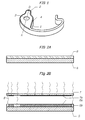
- la Figure 1 est une vue en perspective d'un ressort de rappel à structure monocouche,
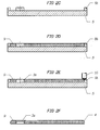
- les Figures 2A à 2F sont des vues en coupe selon la ligne AB de la Figure 1 représentant les différentes étapes de la fabrication du ressort de la Figure 1,
- la Figure 3A est une vue en perspective de dessous, et la Figure 3B est une vue en coupe selon la ligne AB de la Figure 3A, d'une ancre pour échappement de mouvement d'horlogerie,
- les Figures 4A à 4H sont des vues en coupe représentant schématiquement les différentes étapes de la fabrication de l'ancre des Figures 3A et 3B,
- la Figure 5 est une vue en coupe partielle d'un assemblage d'une vis dans un trou taraudé du substrat métallique massif, et dépassant au-dessus de la surface de celui-ci.
- FIG. 1 is a perspective view of a monolayer structure return spring,
- Figures 2A to 2F are sectional views along line AB of Figure 1 representing the various stages of the manufacture of the spring of Figure 1,
- 3A is a perspective view from below, and FIG. 3B is a sectional view along the line AB of FIG. 3A, of a watch movement escapement anchor, FIG.
- FIGS. 4A to 4H are sectional views schematically showing the various steps in the manufacture of the anchor of FIGS. 3A and 3B,
- Figure 5 is a partial sectional view of an assembly of a screw in a tapped hole of the solid metal substrate, and protruding above the surface thereof.
Les exemples ci-après décrivent la fabrication selon le procédé de l'invention de ce ressort de rappel et de cette ancre, en référence aux figures 1 à 4H.The following examples describe the manufacture according to the method of the invention of this return spring and this anchor, with reference to Figures 1 to 4H.
La Figure 1 représente un ressort de rappel avec un côté supérieur 2, un côté inférieur 1, un trou cylindrique 3 et une partie anglée 4. Les dimensions de ce ressort sont les suivantes : épaisseur 0,170 mm (± 7 µm), diamètre 0,412 mm (± 2 µm), largeur de lame 0,046 mm (± 2 µm) et encombrement de l'ordre de 2 mm X 3,5 mm.Figure 1 shows a return spring with an
A la Figure 2A on a représenté la structure obtenue à l'issue de l'étape b) du procédé de la revendication 2, qui comprend une couche de photorésist 6 recouvrant le substrat 5. Cette structure a été obtenue selon le protocole décrit ci-après.FIG. 2A shows the structure obtained after step b) of the method of
Un substrat 5 formé d'une plaquette en acier inox de 1 mm d'épaisseur et de 150 mm de diamètre, a été dégraissé et préparé pour l'électroformage par dégraissage avec une solution alcaline, neutralisation avec une solution acide pour passiver sa surface, puis rinçage à l'eau distillée et séchage. On a ensuite procédé à l'étalement sur le substrat 5 par dépôt à la tournette d'une première couche de photorésist négatif à base de résine époxy octofonctionelle SU-8 de 100 µm d'épaisseur, puis au chauffage pour évaporation du solvant pendant 5 minutes à 65 °C, puis 20 minutes à 95°C. On a ensuite procédé à l'étalement sur la première couche de photorésist par dépôt à la tournette d'une deuxième couche du même photorésist de 100 µm d'épaisseur, puis au chauffage pour évaporation du solvant pendant 5 minutes à 65 °C, puis 45 minutes à 95°C.A
La Figure 2B correspond à l'étape c) de la revendication 2, avec une illumination UV d'environ 500 mi/cm2 centrée à 365 nm du photorésist à travers un masque correspondant à l'empreinte désirée. On distingue sur cette figure le masque comportant un support 7 transparent aux UV et des zones opaques 7a formées par des dépôts de chrome. Le même support formant le masque peut comporter un grand nombre de zones correspondant à autant de structures pouvant être fabriquées en un seul lot, toutes les zones étant obtenues avec une très haute résolution du contour par photolithographie, technique bien connue dans l'industrie microélectronique.Figure 2B corresponds to step c) of
Cette irradiation par rayons UV 8 induit la photopolymérisation de la résine dans les zones exposées 6b, les zones non exposées 6a restant non polymérisées.This
La Figure 2C montre la structure obtenue à l'issue de l'étape e) de la revendication 2. On a effectué un recuit de la couche obtenue à l'issue de l'étape c) pour compléter la polymérisation pendant 1 minute à 65 °C, puis 15 minutes à 95 °C, puis dissolution du photorésist non exposé par passage pendant 15 minutes dans trois bains successifs de PGMEA (de plus en plus pur), rinçage dans un bain d'alcool isopropylique et séchage. On distingue dans la Figure 2C le moule 6b en photorésist polymérisé superposé sur le substrat 5.FIG. 2C shows the structure obtained at the end of step e) of
La Figure 2D montre la structure obtenue à l'issue de l'étape f) de la revendication 2 après dépôt galvanique de nickel, puis mise à niveau par abrasion et polissage de façon à obtenir une surface supérieure plane. On distingue sur cette figure le moule de résine polymérisée 6b et la couche électroformée 9, qui recouvrent le substrat 5.Figure 2D shows the structure obtained after step f) of
La Figure 2E montre la structure obtenue au cours de l'étape g) de la revendication 2 pendant une opération d'anglage. On distingue sur cette figure le substrat 5, la structure métallique 9, le moule de résine polymérisée 6b, le trou anglé 3a et la fraise 10 utilisée pour l'anglage.Figure 2E shows the structure obtained in step g) of
La Figure 2F, qui correspond à la vue en coupe de la Figure 1, montre le ressort obtenu à l'issue de l'étape h) de la revendication 2, après détachage du substrat métallique par délaminage et stripage du photorésist polymérisé avec le N-méthylpyrrolidone.FIG. 2F, which corresponds to the sectional view of FIG. 1, shows the spring obtained at the end of step h) of
Les Figures 3A et 3B représentent une ancre comportant un côté supérieur 1, un côté inférieur 2, un trou cylindrique 3, une fourchette 4 et un dégagement 5. Les dimensions de cette ancre sont les suivantes : épaisseur du premier niveau 0,105 mm (± 5 µm), épaisseur du deuxième niveau 0,07 mm (± 5 µm), épaisseur totale 0,175 mm (± 10 µm), diamètre 0,306 mm (± 1 µm), diamètre selon AB 0,250 mm (± 4 µm), encombrement de l'ordre de 4 mm X 3 mm.Figures 3A and 3B show an anchor having an
A la Figure 4A on a représenté la structure obtenue à l'issue de l'étape b) du procédé de la revendication 3, qui comprend une couche de photorésist 7 recouvrant le substrat 6. Cette structure a été obtenue selon le protocole décrit ci-après.FIG. 4A shows the structure obtained after step b) of the method of
Un substrat 6 formé d'une plaquette en acier inox de 1 mm d'épaisseur et de 150 mm de diamètre, a été dégraissé et préparé pour l'électroformage par dégraissage avec une solution alcaline, neutralisation avec une solution acide pour passiver sa surface, puis rinçage à l'eau distillée et séchage. On a ensuite procédé à l'étalement sur le substrat 5 par dépôt à la tournette d'une première couche de photorésist négatif à base de résine époxy octofonctionelle SU-8 de 70 µm d'épaisseur, puis au chauffage pour évaporation du solvant pendant 3 minutes à 65 °C, puis 9 minutes à 95 °C. On a ensuite procédé à l'étalement sur la première couche de photorésist par dépôt à la tournette d'une deuxième couche du même photorésist de 70 µm d'épaisseur, puis au chauffage pour évaporation du solvant pendant 5 minutes à 65 °C, puis 35 minutes à 95°C.A
La Figure 4B correspond à l'étape c) de la revendication 3 d'illumination UV d'environ 450 mJ/cm2 centrée à 365 nm, du photorésist à travers un masque correspondant à l'empreinte désirée. On distingue sur cette figure le masque comportant un support 8 transparent aux UV et des zones opaques 8a formées par des dépôts de chrome. Cette irradiation par rayons UV 9 induit la photopolymérisation de la résine dans les zones exposées 7b, les zones non exposées 7a restant non polymérisées.Figure 4B corresponds to step c) of
La Figure 4C montre la structure obtenue à l'issue de l'étape e) de la revendication 3. On a effectué un recuit de la couche obtenue à l'issue de l'étape c) pour compléter la polymérisation pendant 1 minute à 65 °C, puis 15 minutes à 95 °C, puis dissout le photorésist non exposé par passage de 15 minutes dans trois bains successifs de PGMEA (de plus en plus pur), rinçage dans un bain d'alcool isopropylique et séchage. On distingue dans cette figure le moule de photorésist polymérisé 7b sur le substrat 6.FIG. 4C shows the structure obtained at the end of step e) of
La Figure 4D montre la structure obtenue après avoir effectué l'étape f) de la revendication 3 de dépôt galvanique de nickel dans les parties ouvertes du moule de photorésist polymérisé, et mise à niveau par abrasion et polissage de façon à obtenir une surface supérieure plane, et reproduit les étapes a) et b) avec deux couches successives de 50 µm du même photorésist à base de résine époxy SU-8, chauffage pendant 3 minutes à 65 °C puis 6 minutes à 95 °C pour la première couche, et chauffage pendant 5 minute à 65 °C puis 20 minutes à 95 °C pour la deuxième couche. On distingue sur la Figure 4D la couche de photorésist 11 recouvrant le photorésist polymérisé 7b et la couche électroformée 10, au-dessus du substrat 6.FIG. 4D shows the structure obtained after carrying out step f) of
La Figure 4E correspond à la reproduction de l'étape c) de la revendication 3 (au cours de l'étape g)), avec une illumination UV d'environ 400 mJ/cm2 centrée à 365 nm, du photorésist à travers un nouveau masque correspondant à l'empreinte désirée. On distingue sur cette figure le masque comportant un support 12 transparent aux UV et des zones opaques 12a formées par des dépôts de chrome. Cette irradiation par rayons UV 9 induit la photopolymérisation de la résine dans les zones exposées 11b, les zones non exposées 11a restant non polymérisées.Figure 4E corresponds to the reproduction of step c) of claim 3 (during step g)), with a UV illumination of about 400 mJ / cm 2 centered at 365 nm, of the photoresist through a new mask corresponding to the desired imprint. This figure shows the mask comprising a
La Figure 4F montre la structure obtenue à l'issue de la reproduction de l'étape e) de la revendication 3 (au cours de l'étape g)). On a effectué un recuit de la couche obtenue à l'issue de la reproduction de l'étape c) pour compléter la polymérisation pendant 1 minute à 65 °C, puis 15 minutes à 95 °C, puis dissous le photorésist non exposé par passage pendant 15 minutes dans trois bains successifs de PGMEA (de pureté croissante), rinçage dans un bain d'alcool isopropylique et séchage. On distingue dans cette figure le deuxième moule de photorésist polymérisé 11b au-dessus du premier moule de photorésist polymérisé 7b et la couche de métal électroformé 10, au-dessus du substrat 6.Figure 4F shows the structure obtained after reproduction of step e) of claim 3 (in step g)). Annealing of the layer obtained from the reproduction of step c) was carried out to complete the polymerization for 1 minute at 65 ° C, then 15 minutes at 95 ° C, and then dissolved the unexposed photoresist. by passing for 15 minutes in three successive baths of PGMEA (of increasing purity), rinsing in an isopropyl alcohol bath and drying. In this figure, the second
La Figure 4G montre la structure obtenue à l'issue de la reproduction de l'étape f) de la revendication 3 (au cours de l'étape h)). On a effectué un deuxième dépôt galvanique du même métal, le nickel, jusqu'à une hauteur légèrement supérieure (de 10 à 30 µm) à l'épaisseur visée, puis mis à niveau par abrasion et polissage de façon à obtenir une surface supérieure plane. On distingue sur cette figure le deuxième moule de résine polymérisée 11b et la deuxième couche électroformée 13, au-dessus du premier moule polymérisé 7b et de la première couche électroformée 10, au-dessus du substrat 6.Figure 4G shows the structure obtained after reproduction of step f) of claim 3 (during step h)). A second galvanic deposition of the same metal, nickel, was performed to a slightly greater height (10 to 30 μm) at the target thickness, then leveled by abrasion and polishing to obtain a flat top surface. . In this figure, the second
La Figure 4H, qui correspond à la vue en coupe de la Figure 3B, montre l'ancre obtenue à l'issue de l'étape k) de la revendication 3, après détachage du substrat métallique par délaminage et élimination du photorésist polymérisé par un traitement plasmatique.FIG. 4H, which corresponds to the sectional view of FIG. 3B, shows the anchor obtained at the end of step k) of
Claims (13)
caractérisé en ce qu'après les étapes a) à e) on place un objet fixé de façon amovible au-dessus du substrat métallique massif, et que lors du détachage par délaminage de la structure métallique et du photorésist polymérisé du substrat métallique massif, on libère cet objet du substrat métallique massif, de façon à obtenir une structure métallique monocouche ou multicouche à couches entièrement superposées comportant un objet inséré.Process according to one of Claims 2 to 6
characterized in that after the steps a) to e) is placed an object removably attached above the solid metal substrate, and that during the delamination stain removal of the metal structure and the polymerized photoresist of the bulk metal substrate, releases this object from the solid metal substrate, so as to obtain a monolayer or multilayer metal structure with fully superposed layers comprising an inserted object.
caractérisé en ce qu'après les étapes a) à e) on place une vis dans un trou taraudé du substrat métallique massif laquelle dépasse au-dessus de la surface supérieure de celui-ci, et que lors du détachage par délaminage de la structure métallique et du photorésist polymérisé du substrat métallique massif, on devisse cette vis, de façon à obtenir une structure métallique monocouche ou multicouche à couches entièrement superposées comportant un trou fileté.Process according to one of Claims 2 to 6
characterized in that after steps a) to e) a screw is placed in a tapped hole of the solid metal substrate which protrudes above the upper surface thereof, and when delaminating the metal structure and the polymerized photoresist of the solid metal substrate, this screw is made, so as to obtain a single layer or multilayer metal structure with fully superposed layers comprising a threaded hole.
Priority Applications (9)
| Application Number | Priority Date | Filing Date | Title |
|---|---|---|---|
| EP06405114A EP1835339B1 (en) | 2006-03-15 | 2006-03-15 | Fabrication process by LIGA type technology, of a monolayer or multilayer metallic structure, and structure obtained therewith |
| DE06405114T DE06405114T1 (en) | 2006-03-15 | 2006-03-15 | LIGA Process for producing a single or multilayer metallic structure and structure produced therewith |
| CN200710085765XA CN101038440B (en) | 2006-03-15 | 2007-03-14 | Process for fabricating a monolayer or multilayer metal structure in LIGA technology, and structure obtained |
| US11/717,773 US8025782B2 (en) | 2006-03-15 | 2007-03-14 | Process for fabricating a monolayer or multilayer metal structure in LIGA technology, and structure obtained |
| JP2007067204A JP5665252B2 (en) | 2006-03-15 | 2007-03-15 | Method for producing single-layer or multi-layer metal structure in LIGA technology and structure obtained thereby |
| HK08102824.0A HK1116260A1 (en) | 2006-03-15 | 2008-03-11 | Fabrication process by liga type technology, of a monolayer or multilayer metallic structure, and structure obtained therewith |
| US12/952,825 US9284654B2 (en) | 2006-03-15 | 2010-11-23 | Process for fabricating a monolayer or multilayer metal structure in LIGA technology, and structure obtained |
| US13/212,636 US9365941B2 (en) | 2006-03-15 | 2011-08-18 | Process for fabricating a monolayer or multilayer metal structure in LIGA technology, and structure obtained |
| JP2014109958A JP5873894B2 (en) | 2006-03-15 | 2014-05-28 | Method for producing single-layer or multi-layer metal structure in LIGA technology and structure obtained thereby |
Applications Claiming Priority (1)
| Application Number | Priority Date | Filing Date | Title |
|---|---|---|---|
| EP06405114A EP1835339B1 (en) | 2006-03-15 | 2006-03-15 | Fabrication process by LIGA type technology, of a monolayer or multilayer metallic structure, and structure obtained therewith |
Publications (2)
| Publication Number | Publication Date |
|---|---|
| EP1835339A1 true EP1835339A1 (en) | 2007-09-19 |
| EP1835339B1 EP1835339B1 (en) | 2012-05-16 |
Family
ID=37028815
Family Applications (1)
| Application Number | Title | Priority Date | Filing Date |
|---|---|---|---|
| EP06405114A Active EP1835339B1 (en) | 2006-03-15 | 2006-03-15 | Fabrication process by LIGA type technology, of a monolayer or multilayer metallic structure, and structure obtained therewith |
Country Status (6)
| Country | Link |
|---|---|
| US (3) | US8025782B2 (en) |
| EP (1) | EP1835339B1 (en) |
| JP (2) | JP5665252B2 (en) |
| CN (1) | CN101038440B (en) |
| DE (1) | DE06405114T1 (en) |
| HK (1) | HK1116260A1 (en) |
Cited By (17)
| Publication number | Priority date | Publication date | Assignee | Title |
|---|---|---|---|---|
| WO2009083488A1 (en) * | 2007-12-31 | 2009-07-09 | Nivarox-Far S.A. | Method for obtaining a metal microstructure and microstructure obtained according to said method |
| EP2182096A1 (en) * | 2008-10-28 | 2010-05-05 | Nivarox-FAR S.A. | Heterogeneous LIGA method |
| WO2010142529A1 (en) * | 2009-06-12 | 2010-12-16 | Nivarox-Far S.A. | Method for manufacturing a metal microstructure and microstructure obtained according to said method |
| EP2557460A1 (en) * | 2011-08-12 | 2013-02-13 | Nivarox-FAR S.A. | Metallic pallets with polymer horns |
| WO2013045706A2 (en) | 2011-09-29 | 2013-04-04 | Rolex S.A. | Integral assembly of a hairspring and a collet |
| EP2586879A1 (en) * | 2011-10-27 | 2013-05-01 | Nivarox-FAR S.A. | Method for thermal treatment of micromechanical clock parts |
| EP2672320A1 (en) | 2012-06-06 | 2013-12-11 | Mimotec S.A. | Method for producing three-dimensional metal micro-parts by growth in a mixed cavity and micro-parts obtained by the method |
| WO2014001017A1 (en) * | 2012-06-28 | 2014-01-03 | Nivarox-Far S.A. | Mainspring for a timepiece |
| EP2767869A1 (en) * | 2013-02-13 | 2014-08-20 | Nivarox-FAR S.A. | Method for manufacturing a one-piece micromechanical part comprising at least two separate levels |
| EP2833204A1 (en) * | 2013-08-02 | 2015-02-04 | Rolex Sa | Method for treating a layer of photosensitive resin and method for manufacturing a metal component |
| EP2913711A1 (en) * | 2014-02-28 | 2015-09-02 | Mimotec S.A. | Method for manufacturing metal parts with inserts by photolithography and electroforming |
| WO2018172895A1 (en) * | 2017-03-24 | 2018-09-27 | Montblanc Montre Sa | Process for manufacturing a metal-ceramic timepiece component |
| EP3614205A1 (en) * | 2018-08-22 | 2020-02-26 | Nivarox-FAR S.A. | Method for manufacturing a timepiece component and component produced by this method |
| EP3789825A1 (en) * | 2019-09-05 | 2021-03-10 | Mimotec S.A. | Method for manufacturing a plurality of microparts |
| EP4350436A1 (en) | 2022-10-07 | 2024-04-10 | Richemont International S.A. | Method for manufacturing mold for forming metal part by metal growth |
| EP4350443A1 (en) | 2022-10-07 | 2024-04-10 | Richemont International S.A. | Mould for forming metal parts by metal growth and method for manufacturing such a mould |
| EP4350439A1 (en) | 2022-10-07 | 2024-04-10 | Richemont International S.A. | Method for producing a mould for forming metal parts by metal growth |
Families Citing this family (37)
| Publication number | Priority date | Publication date | Assignee | Title |
|---|---|---|---|---|
| US8076057B2 (en) * | 2008-02-29 | 2011-12-13 | Corning Incorporated | Methods of making extrusion dies |
| JP5462006B2 (en) * | 2009-02-17 | 2014-04-02 | セイコーインスツル株式会社 | Escape governor, mechanical timepiece, and method of manufacturing ankle body |
| CN102147569B (en) * | 2010-12-02 | 2012-10-10 | 天津海鸥表业集团有限公司 | Processing method of micro-component in multi-layer structure and solidified SU-8 photoresist sheet |
| JP5786459B2 (en) * | 2011-05-31 | 2015-09-30 | 大日本印刷株式会社 | Method for producing metal particles |
| JP5824878B2 (en) * | 2011-05-31 | 2015-12-02 | 大日本印刷株式会社 | Method for producing anti-counterfeit particles |
| JP2014074585A (en) * | 2012-10-02 | 2014-04-24 | Seiko Instruments Inc | Timepiece component and manufacturing method of the same |
| JP5786906B2 (en) * | 2013-08-02 | 2015-09-30 | オムロン株式会社 | Manufacturing method of electroformed parts |
| US9142903B2 (en) * | 2013-11-22 | 2015-09-22 | Tektronix, Inc. | High performance multiport connector system using LIGA springs |
| CN104671191B (en) * | 2013-11-27 | 2017-09-29 | 北京嘉岳同乐极电子有限公司 | micro-nano structure and preparation method thereof |
| EP2937311B1 (en) * | 2014-04-25 | 2019-08-21 | Rolex Sa | Method for manufacturing a reinforced timepiece component, corresponding timepiece component and timepiece |
| EP2977835B1 (en) * | 2014-07-21 | 2017-06-28 | The Swatch Group Research and Development Ltd. | Welding by electroforming an electroformed timepiece shell |
| CN105696037A (en) * | 2014-11-26 | 2016-06-22 | 泰科电子(上海)有限公司 | Electroplating method for workpiece and electroplating protective glue |
| EP3034461B1 (en) * | 2014-12-19 | 2020-07-01 | Rolex Sa | Production of a multi-level clock component |
| EP3035129B1 (en) * | 2014-12-19 | 2020-11-04 | The Swatch Group Research and Development Ltd | Method for producing a decorated element of a timepiece or piece of jewellery |
| JP5930091B2 (en) * | 2015-03-16 | 2016-06-08 | 大日本印刷株式会社 | Method for producing metal particles |
| US10900135B2 (en) * | 2016-02-09 | 2021-01-26 | Weinberg Medical Physics, Inc. | Method and apparatus for manufacturing particles |
| CN106637364B (en) * | 2016-11-30 | 2018-10-16 | 华侨大学 | A kind of parts conveyer equipment of multistation |
| CN106757218B (en) * | 2016-11-30 | 2018-05-25 | 华侨大学 | A kind of hand-operated tools segmentation electro-plating method based on shielded layer mechanical removal equipment |
| CN106591900B (en) * | 2016-11-30 | 2018-08-10 | 华侨大学 | A kind of plating millgrain tool segmentation electro-plating method based on shielded layer mechanical removal equipment |
| CN106637320B (en) * | 2016-11-30 | 2018-08-28 | 华侨大学 | A kind of hand-operated tools segmentation electro-plating method based on shielded layer mechanical removal automatic production line |
| CN106435675B (en) * | 2016-11-30 | 2018-08-28 | 华侨大学 | It is a kind of to be suitable for being segmented the shielded layer cancellation equipment being electroplated and its canceling method |
| CN106591901B (en) * | 2016-11-30 | 2018-08-28 | 华侨大学 | It is a kind of to be suitable for being segmented the shielded layer cancellation automatic production line being electroplated and its method |
| CN106498481B (en) * | 2016-11-30 | 2018-08-10 | 华侨大学 | A kind of plating millgrain tool segmentation electro-plating method for cancelling equipment based on shielded layer chemistry |
| CN106757219B (en) * | 2016-11-30 | 2018-07-20 | 华侨大学 | A kind of hand-operated tools segmentation electro-plating method for cancelling automatic production line based on shielded layer chemistry |
| CN106521584B (en) * | 2016-11-30 | 2018-08-14 | 华侨大学 | A kind of hand-operated tools segmentation electro-plating method for cancelling equipment based on shielded layer chemistry |
| EP3479720B1 (en) * | 2017-11-07 | 2020-03-25 | The Swatch Group Research and Development Ltd | Method for crimping a stone |
| EP3489763B1 (en) * | 2017-11-22 | 2021-06-16 | Nivarox-FAR S.A. | Pallet for watch movement escapement |
| EP3495894B1 (en) * | 2017-12-05 | 2023-01-04 | Rolex Sa | Method for manufacturing a clock component |
| KR102013283B1 (en) * | 2017-12-05 | 2019-08-22 | 재단법인 오송첨단의료산업진흥재단 | Method of detaching a thin film electrode using thermal expansion coefficient |
| US10975486B2 (en) | 2018-03-29 | 2021-04-13 | Unison Industries, Llc | Duct assembly and method of forming |
| US10697076B2 (en) | 2018-03-29 | 2020-06-30 | Unison Industries, Llc | Duct assembly and method of forming |
| US10697075B2 (en) | 2018-03-29 | 2020-06-30 | Unison Industries, Llc | Duct assembly and method of forming |
| US10731486B2 (en) * | 2018-03-29 | 2020-08-04 | Unison Industries, Llc | Duct assembly and method of forming |
| EP3557333B1 (en) * | 2018-04-16 | 2020-11-04 | Patek Philippe SA Genève | Method for manufacturing a timepiece mainspring |
| EP3671367A1 (en) | 2018-12-21 | 2020-06-24 | ETA SA Manufacture Horlogère Suisse | Assembly comprising a support, a plate and attachment means, in particular for a timepiece |
| EP3786722A1 (en) * | 2019-08-27 | 2021-03-03 | Comadur S.A. | Method for decorating a mechanical part |
| CN116234968A (en) | 2021-02-09 | 2023-06-06 | 普和希控股公司 | Drainage cover and refrigeration house |
Citations (6)
| Publication number | Priority date | Publication date | Assignee | Title |
|---|---|---|---|---|
| US5766441A (en) * | 1995-03-29 | 1998-06-16 | Robert Bosch Gmbh | Method for manfacturing an orifice plate |
| EP0851295A1 (en) * | 1996-12-27 | 1998-07-01 | Ecole Polytechnique Federale De Lausanne | Process for the fabrication of microstructures by multilayer conformation of a photosensitive resin et microstructures obtained therewith |
| US20030062652A1 (en) * | 2001-10-03 | 2003-04-03 | Jeong-Bong Lee | Reproduction of micromold inserts |
| EP1331528A2 (en) * | 2002-01-29 | 2003-07-30 | Franck Muller-Watchland SA | Escape pallets for timepiece |
| US20050056074A1 (en) * | 2003-09-12 | 2005-03-17 | Meng Wen Jin | Microscale compression molding of metals with surface engineered LIGA inserts |
| EP1596259A1 (en) * | 2004-05-10 | 2005-11-16 | Precision Engineering AG | Method of manufacture of thin metallic bodies, particularly watch parts |
Family Cites Families (37)
| Publication number | Priority date | Publication date | Assignee | Title |
|---|---|---|---|---|
| DE4142001A1 (en) * | 1991-12-19 | 1993-06-24 | Microparts Gmbh | METHOD FOR PRODUCING STEPPED MOLD INSERTS, STEPPED MOLD INSERTS AND MOLDED MICROSTRUCTURE BODY THEREFOR |
| US2006606A (en) | 1933-03-11 | 1935-07-02 | Joseph F Roman | Yieldable jewel bearing |
| US2080750A (en) * | 1934-03-02 | 1937-05-18 | Ralph E Thompson | Method of making bearings |
| US2645078A (en) | 1949-08-22 | 1953-07-14 | Bulova Arde | Jewel bearing and method of making same |
| US2995443A (en) * | 1957-08-08 | 1961-08-08 | Metalphoto Corp | Aluminum plate with plural images and method of making same |
| US3335562A (en) * | 1965-03-03 | 1967-08-15 | Tissot Horlogerie | Anchor escapement for timepieces |
| JPS5831260B2 (en) * | 1977-12-23 | 1983-07-05 | 株式会社荏原製作所 | Casting method for impeller with screw hole |
| JPS5740669A (en) * | 1980-08-25 | 1982-03-06 | Citizen Watch Co Ltd | Watch hand and manuacture thereof |
| US4394341A (en) * | 1982-02-01 | 1983-07-19 | Rca Corporation | Method to center and separate electroformed replicas from a matrix |
| US4484788A (en) * | 1982-09-08 | 1984-11-27 | Artopex Inc. | Flush pull drawer handle for cabinet |
| IT1182402B (en) * | 1985-02-04 | 1987-10-05 | Olivetti & Co Spa | METHOD ID MANUFACTURE OF METAL ELEMENTS OF INK JET PRINTING AND RELATED PRINTING ELEMENTS |
| NL8603278A (en) * | 1986-12-23 | 1988-07-18 | Stork Veco Bv | MEMBRANE WITH PERFORATIONS AND METHOD FOR MANUFACTURING SUCH MEMBRANE. |
| JP2992647B2 (en) * | 1990-12-17 | 1999-12-20 | 九州日立マクセル株式会社 | Method for producing electroformed product having through-hole |
| JPH0594937A (en) * | 1991-10-01 | 1993-04-16 | Sumitomo Electric Ind Ltd | Formation method of fine structure body |
| JP3410798B2 (en) * | 1994-03-11 | 2003-05-26 | 株式会社センシュー | Mold and casting method using this mold |
| CN1144944C (en) * | 1995-03-29 | 2004-04-07 | 罗伯特·博施有限公司 | Perforated disc especially for injection valves |
| US5775219A (en) * | 1995-12-13 | 1998-07-07 | Kyushu Hitachi Maxell, Ltd. | Squeegee for screen printing |
| EP1015669B1 (en) * | 1997-04-04 | 2010-11-17 | University Of Southern California | Electroplating method for forming a multilayer structure |
| NL1009106C2 (en) * | 1998-05-08 | 1999-11-09 | Od & Me Bv | Method of manufacturing a stamper, stamper obtained by such a method, and optical disk obtained by using such a stamper. |
| CN1184351C (en) * | 1999-03-30 | 2005-01-12 | 中国科学院高能物理研究所 | Upper sacrificial layer processing method |
| US6350360B1 (en) * | 2000-04-07 | 2002-02-26 | Sandia Coroporation | Method of fabricating a 3-dimensional tool master |
| JP3364195B2 (en) * | 2000-06-05 | 2003-01-08 | テフコ青森株式会社 | Patterned electrodeposited image and manufacturing method thereof |
| JP3668868B2 (en) * | 2000-12-22 | 2005-07-06 | トヨタ自動車株式会社 | Cap nut casting method and cast member |
| US6755566B2 (en) * | 2001-02-15 | 2004-06-29 | Konrad Damasko | Clockwork |
| TW495843B (en) * | 2001-05-11 | 2002-07-21 | Macronix Int Co Ltd | Method for reducing photoresist roughness by crosslinking photoresist with deposited material |
| SE523309E (en) * | 2001-06-15 | 2009-10-26 | Replisaurus Technologies Ab | Method, electrode and apparatus for creating micro- and nanostructures in conductive materials by patterning with master electrode and electrolyte |
| JP3820480B2 (en) * | 2001-08-09 | 2006-09-13 | 株式会社ティ・アンド・ティホールディングス | A pair of shafts and resin bearing parts and method of manufacturing the same |
| JP3903780B2 (en) * | 2001-11-30 | 2007-04-11 | 住友電気工業株式会社 | Manufacturing method of fine parts |
| JP2004009144A (en) * | 2002-06-03 | 2004-01-15 | Disco Abrasive Syst Ltd | Method of manufacturing micro parts |
| US7105280B1 (en) * | 2002-06-28 | 2006-09-12 | Seagate Technology Llc | Utilizing permanent master for making stampers/imprinters for patterning of recording media |
| JP2005007445A (en) * | 2003-06-19 | 2005-01-13 | Kanto Auto Works Ltd | Manufacturing method for casting having screw hole |
| JP2005007444A (en) * | 2003-06-19 | 2005-01-13 | Kanto Auto Works Ltd | Manufacturing method for casting having screw hole, and nut for casting |
| JP4366140B2 (en) * | 2003-08-06 | 2009-11-18 | サミー株式会社 | Board case |
| JP2005129428A (en) * | 2003-10-27 | 2005-05-19 | Sumitomo Electric Ind Ltd | Manufacturing method for telescopic contact, contact manufactured by the method and inspection device or electronic instrument provided with the contact |
| JP4530261B2 (en) * | 2004-03-31 | 2010-08-25 | セイコーインスツル株式会社 | Electroformed part and method for producing electroformed part |
| CN1288069C (en) * | 2004-06-03 | 2006-12-06 | 上海交通大学 | Method for integral micromachining multilayer composite structure |
| JP2006052448A (en) * | 2004-08-12 | 2006-02-23 | Tefuko Aomori Kk | Patterned metal sheet and preparing method therefor |
-
2006
- 2006-03-15 EP EP06405114A patent/EP1835339B1/en active Active
- 2006-03-15 DE DE06405114T patent/DE06405114T1/en active Pending
-
2007
- 2007-03-14 US US11/717,773 patent/US8025782B2/en active Active
- 2007-03-14 CN CN200710085765XA patent/CN101038440B/en active Active
- 2007-03-15 JP JP2007067204A patent/JP5665252B2/en active Active
-
2008
- 2008-03-11 HK HK08102824.0A patent/HK1116260A1/en not_active IP Right Cessation
-
2010
- 2010-11-23 US US12/952,825 patent/US9284654B2/en active Active
-
2011
- 2011-08-18 US US13/212,636 patent/US9365941B2/en active Active
-
2014
- 2014-05-28 JP JP2014109958A patent/JP5873894B2/en not_active Expired - Fee Related
Patent Citations (6)
| Publication number | Priority date | Publication date | Assignee | Title |
|---|---|---|---|---|
| US5766441A (en) * | 1995-03-29 | 1998-06-16 | Robert Bosch Gmbh | Method for manfacturing an orifice plate |
| EP0851295A1 (en) * | 1996-12-27 | 1998-07-01 | Ecole Polytechnique Federale De Lausanne | Process for the fabrication of microstructures by multilayer conformation of a photosensitive resin et microstructures obtained therewith |
| US20030062652A1 (en) * | 2001-10-03 | 2003-04-03 | Jeong-Bong Lee | Reproduction of micromold inserts |
| EP1331528A2 (en) * | 2002-01-29 | 2003-07-30 | Franck Muller-Watchland SA | Escape pallets for timepiece |
| US20050056074A1 (en) * | 2003-09-12 | 2005-03-17 | Meng Wen Jin | Microscale compression molding of metals with surface engineered LIGA inserts |
| EP1596259A1 (en) * | 2004-05-10 | 2005-11-16 | Precision Engineering AG | Method of manufacture of thin metallic bodies, particularly watch parts |
Non-Patent Citations (1)
| Title |
|---|
| DAS S S ET AL: "Adhesion promotion by surface-modification at the PMMA-metal interface for LIGA-type processing", MICROELECTROMECHANICAL STRUCTURES FOR MATERIALS RESEARCH. SYMPOSIUM MATER. RES. SOC WARRENDALE, PA, USA, 1998, pages 149 - 154, XP008069843, ISBN: 1-55899-424-6 * |
Cited By (41)
| Publication number | Priority date | Publication date | Assignee | Title |
|---|---|---|---|---|
| WO2009083488A1 (en) * | 2007-12-31 | 2009-07-09 | Nivarox-Far S.A. | Method for obtaining a metal microstructure and microstructure obtained according to said method |
| US8557506B2 (en) | 2007-12-31 | 2013-10-15 | Nivarox-Far S.A. | Method of fabricating a metallic microstructure and microstructure obtained via the method |
| US8470154B2 (en) | 2008-10-28 | 2013-06-25 | Nivarox-Far S.A. | Heterogeneous LIGA method |
| EP2182096A1 (en) * | 2008-10-28 | 2010-05-05 | Nivarox-FAR S.A. | Heterogeneous LIGA method |
| WO2010049246A1 (en) * | 2008-10-28 | 2010-05-06 | Nivarox-Far S.A. | Heterogenous liga method |
| WO2010142529A1 (en) * | 2009-06-12 | 2010-12-16 | Nivarox-Far S.A. | Method for manufacturing a metal microstructure and microstructure obtained according to said method |
| EP2263972A1 (en) * | 2009-06-12 | 2010-12-22 | Nivarox-FAR S.A. | Method for manufacturing a metal microstructure and microstructure obtained according to this method |
| US9194052B2 (en) | 2009-06-12 | 2015-11-24 | Nivarox-Far S.A. | Method of fabricating a plurality of metallic microstructures |
| RU2528522C2 (en) * | 2009-06-12 | 2014-09-20 | Ниварокс-Фар С.А. | Making of metal microstructure and microstructure thus made |
| US9015921B2 (en) | 2011-08-12 | 2015-04-28 | Nivarox-Far S.A. | Metal pallets with polymer horns |
| EP2557461A1 (en) * | 2011-08-12 | 2013-02-13 | Nivarox-FAR S.A. | Metal anchor with polymer horns |
| EP2557460A1 (en) * | 2011-08-12 | 2013-02-13 | Nivarox-FAR S.A. | Metallic pallets with polymer horns |
| WO2013045706A2 (en) | 2011-09-29 | 2013-04-04 | Rolex S.A. | Integral assembly of a hairspring and a collet |
| US9411314B2 (en) | 2011-09-29 | 2016-08-09 | Rolex Sa | Integral assembly of a hairspring and a collet |
| EP4224257A1 (en) | 2011-09-29 | 2023-08-09 | Rolex Sa | Monolithic spiral spring - collet assembly |
| EP2586879A1 (en) * | 2011-10-27 | 2013-05-01 | Nivarox-FAR S.A. | Method for thermal treatment of micromechanical clock parts |
| EP2586880A1 (en) * | 2011-10-27 | 2013-05-01 | Nivarox-FAR S.A. | Verfahren zur thermischen Behandlung von mikromechanischen Bauteilen von Uhren |
| US9359652B2 (en) | 2011-10-27 | 2016-06-07 | Nivarox-Far S.A. | Thermal treatment method for micromechanical horological parts |
| EP2672320A1 (en) | 2012-06-06 | 2013-12-11 | Mimotec S.A. | Method for producing three-dimensional metal micro-parts by growth in a mixed cavity and micro-parts obtained by the method |
| EP2672319A1 (en) | 2012-06-06 | 2013-12-11 | Mimotec S.A. | Method for producing three-dimensional metal micro-parts by growth in a mixed cavity and micro-parts obtained by the method |
| WO2014001017A1 (en) * | 2012-06-28 | 2014-01-03 | Nivarox-Far S.A. | Mainspring for a timepiece |
| US9329571B2 (en) | 2012-06-28 | 2016-05-03 | Nivarox-Far S.A. | Mainspring for a timepiece |
| EP2767870A3 (en) * | 2013-02-13 | 2015-07-08 | Nivarox-FAR S.A. | Method for manufacturing a one-piece micromechanical part comprising at least two separate functional levels |
| US9197183B2 (en) | 2013-02-13 | 2015-11-24 | Nivarox-Far S.A. | Method of fabricating a single-piece micromechanical component including at least two distinct functional levels |
| EP2767869A1 (en) * | 2013-02-13 | 2014-08-20 | Nivarox-FAR S.A. | Method for manufacturing a one-piece micromechanical part comprising at least two separate levels |
| EP2833204A1 (en) * | 2013-08-02 | 2015-02-04 | Rolex Sa | Method for treating a layer of photosensitive resin and method for manufacturing a metal component |
| EP2913711A1 (en) * | 2014-02-28 | 2015-09-02 | Mimotec S.A. | Method for manufacturing metal parts with inserts by photolithography and electroforming |
| EP2913710A1 (en) * | 2014-02-28 | 2015-09-02 | Mimotec S.A. | Method for manufacturing metal parts with inserts by photolithography and electroforming |
| WO2018172895A1 (en) * | 2017-03-24 | 2018-09-27 | Montblanc Montre Sa | Process for manufacturing a metal-ceramic timepiece component |
| EP3614205A1 (en) * | 2018-08-22 | 2020-02-26 | Nivarox-FAR S.A. | Method for manufacturing a timepiece component and component produced by this method |
| WO2020039032A1 (en) * | 2018-08-22 | 2020-02-27 | Nivarox-Far S.A. | Method for producing a clock-making component and component produced according to said method |
| CN112513735A (en) * | 2018-08-22 | 2021-03-16 | 尼瓦洛克斯-法尔股份有限公司 | Method for manufacturing a timepiece component and component obtained by such a method |
| US11181868B2 (en) | 2018-08-22 | 2021-11-23 | Nivarox-Far S.A. | Method for manufacturing a timepiece component and component obtained by this method |
| EP4012498A1 (en) * | 2019-09-05 | 2022-06-15 | Mimotec S.A. | Method for manufacturing a plurality of microparts |
| EP3789825A1 (en) * | 2019-09-05 | 2021-03-10 | Mimotec S.A. | Method for manufacturing a plurality of microparts |
| EP4350436A1 (en) | 2022-10-07 | 2024-04-10 | Richemont International S.A. | Method for manufacturing mold for forming metal part by metal growth |
| EP4350438A1 (en) | 2022-10-07 | 2024-04-10 | Richemont International S.A. | Method for manufacturing mold for forming metal part by metal growth |
| EP4350443A1 (en) | 2022-10-07 | 2024-04-10 | Richemont International S.A. | Mould for forming metal parts by metal growth and method for manufacturing such a mould |
| EP4350439A1 (en) | 2022-10-07 | 2024-04-10 | Richemont International S.A. | Method for producing a mould for forming metal parts by metal growth |
| EP4350444A1 (en) | 2022-10-07 | 2024-04-10 | Richemont International S.A. | Mould for forming metal parts by metal growth and method for manufacturing such a mould |
| EP4350437A1 (en) | 2022-10-07 | 2024-04-10 | Richemont International S.A. | Method for manufacturing a mould for forming metal parts by metal growth |
Also Published As
| Publication number | Publication date |
|---|---|
| US9284654B2 (en) | 2016-03-15 |
| EP1835339B1 (en) | 2012-05-16 |
| DE06405114T1 (en) | 2008-04-24 |
| US9365941B2 (en) | 2016-06-14 |
| US8025782B2 (en) | 2011-09-27 |
| CN101038440B (en) | 2012-05-30 |
| JP5665252B2 (en) | 2015-02-04 |
| CN101038440A (en) | 2007-09-19 |
| HK1116260A1 (en) | 2008-12-19 |
| US20070227893A1 (en) | 2007-10-04 |
| JP2007247067A (en) | 2007-09-27 |
| US20110303546A1 (en) | 2011-12-15 |
| US20110062112A1 (en) | 2011-03-17 |
| JP5873894B2 (en) | 2016-03-01 |
| JP2014159645A (en) | 2014-09-04 |
Similar Documents
| Publication | Publication Date | Title |
|---|---|---|
| EP1835339B1 (en) | Fabrication process by LIGA type technology, of a monolayer or multilayer metallic structure, and structure obtained therewith | |
| EP2004881B1 (en) | Process for the fabrication of liga-uv multilayer metallic structures, the layers being adjacent and not completely superimposed, and structure therefrom. | |
| EP2229470B1 (en) | Method for obtaining a metal microstructure and microstructure obtained according to said method | |
| EP2347036B1 (en) | Heterogenous liga method | |
| EP2316056B1 (en) | Process for fabricating multi-level metal parts by the uv-liga technique | |
| EP2440690B1 (en) | Method for manufacturing a metal microstructure | |
| RU2562923C2 (en) | Production of substrate with etching mask and making of article with pattern | |
| CH704955B1 (en) | A method of manufacturing a metal microstructure and microstructure obtained using this prodédé. | |
| EP3802920B1 (en) | Method for producing a metal decoration on a dial and dial obtained according to said method | |
| EP3453787B1 (en) | Method for manufacturing a batch of multi-level micromechanical metal parts | |
| EP3467151A1 (en) | Electroplating mould and method for manufacturing same | |
| CH699416A2 (en) | Fabricating multi-level metallic e.g. steel microstructure by UV photolithography and galvanic deposition, comprises covering conductive surface of substrate by first layer of photosensitive resin, and irradiating first layer through mask | |
| EP2833204B1 (en) | Method for treating a layer of photosensitive resin and method for manufacturing a metal component | |
| CH699803A2 (en) | LIGA process heterogeneous. | |
| JP2006001042A (en) | Manufacturing method of mold for optical part and mold for optical part | |
| CH714227A2 (en) | Mold for electroplating and its manufacturing process. | |
| CH701260A2 (en) | Method for metal microstructure and microstructure obtained from the method. |
Legal Events
| Date | Code | Title | Description |
|---|---|---|---|
| PUAI | Public reference made under article 153(3) epc to a published international application that has entered the european phase |
Free format text: ORIGINAL CODE: 0009012 |
|
| AK | Designated contracting states |
Kind code of ref document: A1 Designated state(s): AT BE BG CH CY CZ DE DK EE ES FI FR GB GR HU IE IS IT LI LT LU LV MC NL PL PT RO SE SI SK TR |
|
| AX | Request for extension of the european patent |
Extension state: AL BA HR MK YU |
|
| 17P | Request for examination filed |
Effective date: 20071022 |
|
| GBC | Gb: translation of claims filed (gb section 78(7)/1977) | ||
| 17Q | First examination report despatched |
Effective date: 20071214 |
|
| DET | De: translation of patent claims | ||
| AKX | Designation fees paid |
Designated state(s): CH DE FR GB LI |
|
| REG | Reference to a national code |
Ref country code: HK Ref legal event code: DE Ref document number: 1116260 Country of ref document: HK |
|
| GRAP | Despatch of communication of intention to grant a patent |
Free format text: ORIGINAL CODE: EPIDOSNIGR1 |
|
| GRAS | Grant fee paid |
Free format text: ORIGINAL CODE: EPIDOSNIGR3 |
|
| RAP1 | Party data changed (applicant data changed or rights of an application transferred) |
Owner name: ROLEX S.A. |
|
| GRAA | (expected) grant |
Free format text: ORIGINAL CODE: 0009210 |
|
| AK | Designated contracting states |
Kind code of ref document: B1 Designated state(s): CH DE FR GB LI |
|
| REG | Reference to a national code |
Ref country code: GB Ref legal event code: FG4D Free format text: NOT ENGLISH |
|
| REG | Reference to a national code |
Ref country code: CH Ref legal event code: EP |
|
| REG | Reference to a national code |
Ref country code: CH Ref legal event code: NV Representative=s name: MOINAS & SAVOYE SA |
|
| REG | Reference to a national code |
Ref country code: DE Ref legal event code: R096 Ref document number: 602006029417 Country of ref document: DE Effective date: 20120712 |
|
| REG | Reference to a national code |
Ref country code: HK Ref legal event code: GR Ref document number: 1116260 Country of ref document: HK |
|
| PLBI | Opposition filed |
Free format text: ORIGINAL CODE: 0009260 |
|
| PLAX | Notice of opposition and request to file observation + time limit sent |
Free format text: ORIGINAL CODE: EPIDOSNOBS2 |
|
| 26 | Opposition filed |
Opponent name: MIMOTEC S.A. Effective date: 20130214 |
|
| REG | Reference to a national code |
Ref country code: DE Ref legal event code: R026 Ref document number: 602006029417 Country of ref document: DE Effective date: 20130214 |
|
| PLBB | Reply of patent proprietor to notice(s) of opposition received |
Free format text: ORIGINAL CODE: EPIDOSNOBS3 |
|
| PLBP | Opposition withdrawn |
Free format text: ORIGINAL CODE: 0009264 |
|
| PLBD | Termination of opposition procedure: decision despatched |
Free format text: ORIGINAL CODE: EPIDOSNOPC1 |
|
| PLBM | Termination of opposition procedure: date of legal effect published |
Free format text: ORIGINAL CODE: 0009276 |
|
| STAA | Information on the status of an ep patent application or granted ep patent |
Free format text: STATUS: OPPOSITION PROCEDURE CLOSED |
|
| 27C | Opposition proceedings terminated |
Effective date: 20140102 |
|
| REG | Reference to a national code |
Ref country code: FR Ref legal event code: PLFP Year of fee payment: 11 |
|
| REG | Reference to a national code |
Ref country code: CH Ref legal event code: PFA Owner name: ROLEX S.A., CH Free format text: FORMER OWNER: ROLEX S.A., CH |
|
| REG | Reference to a national code |
Ref country code: FR Ref legal event code: PLFP Year of fee payment: 12 |
|
| REG | Reference to a national code |
Ref country code: FR Ref legal event code: PLFP Year of fee payment: 13 |
|
| PGFP | Annual fee paid to national office [announced via postgrant information from national office to epo] |
Ref country code: FR Payment date: 20230320 Year of fee payment: 18 |
|
| PGFP | Annual fee paid to national office [announced via postgrant information from national office to epo] |
Ref country code: GB Payment date: 20230324 Year of fee payment: 18 Ref country code: DE Payment date: 20230307 Year of fee payment: 18 |
|
| P01 | Opt-out of the competence of the unified patent court (upc) registered |
Effective date: 20230528 |
|
| PGFP | Annual fee paid to national office [announced via postgrant information from national office to epo] |
Ref country code: CH Payment date: 20230402 Year of fee payment: 18 |