EP4350438A1 - Method for manufacturing mold for forming metal part by metal growth - Google Patents
Method for manufacturing mold for forming metal part by metal growth Download PDFInfo
- Publication number
- EP4350438A1 EP4350438A1 EP23202044.6A EP23202044A EP4350438A1 EP 4350438 A1 EP4350438 A1 EP 4350438A1 EP 23202044 A EP23202044 A EP 23202044A EP 4350438 A1 EP4350438 A1 EP 4350438A1
- Authority
- EP
- European Patent Office
- Prior art keywords
- cavities
- layer
- manufacturing
- conductive
- photosensitive resin
- Prior art date
- Legal status (The legal status is an assumption and is not a legal conclusion. Google has not performed a legal analysis and makes no representation as to the accuracy of the status listed.)
- Pending
Links
- 229910052751 metal Inorganic materials 0.000 title claims abstract description 98
- 239000002184 metal Substances 0.000 title claims abstract description 98
- 238000004519 manufacturing process Methods 0.000 title claims abstract description 70
- 230000012010 growth Effects 0.000 title claims abstract description 52
- 238000000034 method Methods 0.000 title claims abstract description 30
- 229920005989 resin Polymers 0.000 claims abstract description 120
- 239000011347 resin Substances 0.000 claims abstract description 120
- 239000000758 substrate Substances 0.000 claims abstract description 33
- 238000009713 electroplating Methods 0.000 claims abstract description 25
- 230000037452 priming Effects 0.000 claims abstract description 11
- 238000000465 moulding Methods 0.000 claims abstract description 6
- 239000010410 layer Substances 0.000 claims description 133
- 238000000151 deposition Methods 0.000 claims description 26
- 238000010438 heat treatment Methods 0.000 claims description 26
- 239000000463 material Substances 0.000 claims description 23
- PCHJSUWPFVWCPO-UHFFFAOYSA-N gold Chemical compound [Au] PCHJSUWPFVWCPO-UHFFFAOYSA-N 0.000 claims description 22
- 229910052737 gold Inorganic materials 0.000 claims description 22
- 239000010931 gold Substances 0.000 claims description 22
- 230000008021 deposition Effects 0.000 claims description 19
- YEJRWHAVMIAJKC-UHFFFAOYSA-N 4-Butyrolactone Chemical compound O=C1CCCO1 YEJRWHAVMIAJKC-UHFFFAOYSA-N 0.000 claims description 18
- BGTOWKSIORTVQH-UHFFFAOYSA-N cyclopentanone Chemical compound O=C1CCCC1 BGTOWKSIORTVQH-UHFFFAOYSA-N 0.000 claims description 18
- 230000008569 process Effects 0.000 claims description 16
- 238000005325 percolation Methods 0.000 claims description 12
- 238000005240 physical vapour deposition Methods 0.000 claims description 12
- VYZAMTAEIAYCRO-UHFFFAOYSA-N Chromium Chemical compound [Cr] VYZAMTAEIAYCRO-UHFFFAOYSA-N 0.000 claims description 11
- 238000004070 electrodeposition Methods 0.000 claims description 11
- KDLHZDBZIXYQEI-UHFFFAOYSA-N Palladium Chemical compound [Pd] KDLHZDBZIXYQEI-UHFFFAOYSA-N 0.000 claims description 10
- 239000003999 initiator Substances 0.000 claims description 10
- BASFCYQUMIYNBI-UHFFFAOYSA-N platinum Chemical compound [Pt] BASFCYQUMIYNBI-UHFFFAOYSA-N 0.000 claims description 10
- 230000015572 biosynthetic process Effects 0.000 claims description 9
- RTAQQCXQSZGOHL-UHFFFAOYSA-N Titanium Chemical compound [Ti] RTAQQCXQSZGOHL-UHFFFAOYSA-N 0.000 claims description 7
- 239000012790 adhesive layer Substances 0.000 claims description 7
- 229910052804 chromium Inorganic materials 0.000 claims description 7
- 239000011651 chromium Substances 0.000 claims description 7
- 229910052719 titanium Inorganic materials 0.000 claims description 7
- 239000010936 titanium Substances 0.000 claims description 7
- RYGMFSIKBFXOCR-UHFFFAOYSA-N Copper Chemical compound [Cu] RYGMFSIKBFXOCR-UHFFFAOYSA-N 0.000 claims description 6
- 239000002253 acid Substances 0.000 claims description 6
- 229910052802 copper Inorganic materials 0.000 claims description 6
- 239000010949 copper Substances 0.000 claims description 6
- 230000005855 radiation Effects 0.000 claims description 6
- 229910052715 tantalum Inorganic materials 0.000 claims description 6
- GUVRBAGPIYLISA-UHFFFAOYSA-N tantalum atom Chemical compound [Ta] GUVRBAGPIYLISA-UHFFFAOYSA-N 0.000 claims description 6
- 239000003822 epoxy resin Substances 0.000 claims description 5
- 239000003960 organic solvent Substances 0.000 claims description 5
- 229910052763 palladium Inorganic materials 0.000 claims description 5
- 229910052697 platinum Inorganic materials 0.000 claims description 5
- 229920000647 polyepoxide Polymers 0.000 claims description 5
- RUOJZAUFBMNUDX-UHFFFAOYSA-N propylene carbonate Chemical compound CC1COC(=O)O1 RUOJZAUFBMNUDX-UHFFFAOYSA-N 0.000 claims description 5
- 229910052709 silver Inorganic materials 0.000 claims description 5
- 239000004332 silver Substances 0.000 claims description 5
- 125000005409 triarylsulfonium group Chemical group 0.000 claims description 5
- BQCADISMDOOEFD-UHFFFAOYSA-N Silver Chemical compound [Ag] BQCADISMDOOEFD-UHFFFAOYSA-N 0.000 claims description 4
- 230000008018 melting Effects 0.000 claims description 4
- 238000002844 melting Methods 0.000 claims description 4
- 239000000126 substance Substances 0.000 claims description 2
- 239000004020 conductor Substances 0.000 claims 1
- 239000002904 solvent Substances 0.000 description 45
- 230000007547 defect Effects 0.000 description 13
- 239000000203 mixture Substances 0.000 description 13
- 238000009832 plasma treatment Methods 0.000 description 12
- 238000005289 physical deposition Methods 0.000 description 11
- 229920000642 polymer Polymers 0.000 description 11
- 238000011161 development Methods 0.000 description 10
- KFZMGEQAYNKOFK-UHFFFAOYSA-N Isopropanol Chemical compound CC(C)O KFZMGEQAYNKOFK-UHFFFAOYSA-N 0.000 description 9
- CSCPPACGZOOCGX-UHFFFAOYSA-N Acetone Chemical compound CC(C)=O CSCPPACGZOOCGX-UHFFFAOYSA-N 0.000 description 8
- 239000012808 vapor phase Substances 0.000 description 8
- 239000007789 gas Substances 0.000 description 7
- 230000000977 initiatory effect Effects 0.000 description 7
- 230000005012 migration Effects 0.000 description 7
- 238000013508 migration Methods 0.000 description 7
- 150000003839 salts Chemical class 0.000 description 7
- 239000007787 solid Substances 0.000 description 7
- XUIMIQQOPSSXEZ-UHFFFAOYSA-N Silicon Chemical compound [Si] XUIMIQQOPSSXEZ-UHFFFAOYSA-N 0.000 description 6
- 239000000470 constituent Substances 0.000 description 6
- LLHKCFNBLRBOGN-UHFFFAOYSA-N propylene glycol methyl ether acetate Chemical compound COCC(C)OC(C)=O LLHKCFNBLRBOGN-UHFFFAOYSA-N 0.000 description 6
- 239000007788 liquid Substances 0.000 description 5
- 150000007513 acids Chemical class 0.000 description 4
- 238000000137 annealing Methods 0.000 description 4
- 238000009792 diffusion process Methods 0.000 description 4
- 230000003071 parasitic effect Effects 0.000 description 4
- 229920002120 photoresistant polymer Polymers 0.000 description 4
- 229920001223 polyethylene glycol Polymers 0.000 description 4
- 229920000036 polyvinylpyrrolidone Polymers 0.000 description 4
- 239000001267 polyvinylpyrrolidone Substances 0.000 description 4
- 235000013855 polyvinylpyrrolidone Nutrition 0.000 description 4
- 238000004132 cross linking Methods 0.000 description 3
- 230000007423 decrease Effects 0.000 description 3
- 230000004927 fusion Effects 0.000 description 3
- 238000001465 metallisation Methods 0.000 description 3
- 239000002245 particle Substances 0.000 description 3
- 239000012071 phase Substances 0.000 description 3
- 239000010703 silicon Substances 0.000 description 3
- 229910052710 silicon Inorganic materials 0.000 description 3
- 238000005019 vapor deposition process Methods 0.000 description 3
- 239000002202 Polyethylene glycol Substances 0.000 description 2
- 239000003054 catalyst Substances 0.000 description 2
- 239000000919 ceramic Substances 0.000 description 2
- 239000003795 chemical substances by application Substances 0.000 description 2
- 239000011248 coating agent Substances 0.000 description 2
- 238000000576 coating method Methods 0.000 description 2
- 230000000694 effects Effects 0.000 description 2
- 238000009472 formulation Methods 0.000 description 2
- 239000011521 glass Substances 0.000 description 2
- 238000007373 indentation Methods 0.000 description 2
- 230000001678 irradiating effect Effects 0.000 description 2
- 238000005259 measurement Methods 0.000 description 2
- 230000003287 optical effect Effects 0.000 description 2
- 238000000206 photolithography Methods 0.000 description 2
- 238000004626 scanning electron microscopy Methods 0.000 description 2
- 239000011877 solvent mixture Substances 0.000 description 2
- 238000009987 spinning Methods 0.000 description 2
- 238000004627 transmission electron microscopy Methods 0.000 description 2
- 238000006677 Appel reaction Methods 0.000 description 1
- 241001080024 Telles Species 0.000 description 1
- 230000002378 acidificating effect Effects 0.000 description 1
- 239000000853 adhesive Substances 0.000 description 1
- 230000001070 adhesive effect Effects 0.000 description 1
- 150000001768 cations Chemical class 0.000 description 1
- 239000003638 chemical reducing agent Substances 0.000 description 1
- 239000003086 colorant Substances 0.000 description 1
- 230000000295 complement effect Effects 0.000 description 1
- 238000004090 dissolution Methods 0.000 description 1
- 230000005611 electricity Effects 0.000 description 1
- 238000000572 ellipsometry Methods 0.000 description 1
- 239000012535 impurity Substances 0.000 description 1
- 238000001459 lithography Methods 0.000 description 1
- 239000007769 metal material Substances 0.000 description 1
- 238000012986 modification Methods 0.000 description 1
- 230000004048 modification Effects 0.000 description 1
- 238000006722 reduction reaction Methods 0.000 description 1
- 238000002310 reflectometry Methods 0.000 description 1
- 238000012360 testing method Methods 0.000 description 1
Images


Classifications
-
- C—CHEMISTRY; METALLURGY
- C23—COATING METALLIC MATERIAL; COATING MATERIAL WITH METALLIC MATERIAL; CHEMICAL SURFACE TREATMENT; DIFFUSION TREATMENT OF METALLIC MATERIAL; COATING BY VACUUM EVAPORATION, BY SPUTTERING, BY ION IMPLANTATION OR BY CHEMICAL VAPOUR DEPOSITION, IN GENERAL; INHIBITING CORROSION OF METALLIC MATERIAL OR INCRUSTATION IN GENERAL
- C23C—COATING METALLIC MATERIAL; COATING MATERIAL WITH METALLIC MATERIAL; SURFACE TREATMENT OF METALLIC MATERIAL BY DIFFUSION INTO THE SURFACE, BY CHEMICAL CONVERSION OR SUBSTITUTION; COATING BY VACUUM EVAPORATION, BY SPUTTERING, BY ION IMPLANTATION OR BY CHEMICAL VAPOUR DEPOSITION, IN GENERAL
- C23C14/00—Coating by vacuum evaporation, by sputtering or by ion implantation of the coating forming material
- C23C14/06—Coating by vacuum evaporation, by sputtering or by ion implantation of the coating forming material characterised by the coating material
- C23C14/14—Metallic material, boron or silicon
-
- C—CHEMISTRY; METALLURGY
- C23—COATING METALLIC MATERIAL; COATING MATERIAL WITH METALLIC MATERIAL; CHEMICAL SURFACE TREATMENT; DIFFUSION TREATMENT OF METALLIC MATERIAL; COATING BY VACUUM EVAPORATION, BY SPUTTERING, BY ION IMPLANTATION OR BY CHEMICAL VAPOUR DEPOSITION, IN GENERAL; INHIBITING CORROSION OF METALLIC MATERIAL OR INCRUSTATION IN GENERAL
- C23C—COATING METALLIC MATERIAL; COATING MATERIAL WITH METALLIC MATERIAL; SURFACE TREATMENT OF METALLIC MATERIAL BY DIFFUSION INTO THE SURFACE, BY CHEMICAL CONVERSION OR SUBSTITUTION; COATING BY VACUUM EVAPORATION, BY SPUTTERING, BY ION IMPLANTATION OR BY CHEMICAL VAPOUR DEPOSITION, IN GENERAL
- C23C14/00—Coating by vacuum evaporation, by sputtering or by ion implantation of the coating forming material
- C23C14/0015—Coating by vacuum evaporation, by sputtering or by ion implantation of the coating forming material characterized by the colour of the layer
-
- C—CHEMISTRY; METALLURGY
- C23—COATING METALLIC MATERIAL; COATING MATERIAL WITH METALLIC MATERIAL; CHEMICAL SURFACE TREATMENT; DIFFUSION TREATMENT OF METALLIC MATERIAL; COATING BY VACUUM EVAPORATION, BY SPUTTERING, BY ION IMPLANTATION OR BY CHEMICAL VAPOUR DEPOSITION, IN GENERAL; INHIBITING CORROSION OF METALLIC MATERIAL OR INCRUSTATION IN GENERAL
- C23C—COATING METALLIC MATERIAL; COATING MATERIAL WITH METALLIC MATERIAL; SURFACE TREATMENT OF METALLIC MATERIAL BY DIFFUSION INTO THE SURFACE, BY CHEMICAL CONVERSION OR SUBSTITUTION; COATING BY VACUUM EVAPORATION, BY SPUTTERING, BY ION IMPLANTATION OR BY CHEMICAL VAPOUR DEPOSITION, IN GENERAL
- C23C14/00—Coating by vacuum evaporation, by sputtering or by ion implantation of the coating forming material
- C23C14/22—Coating by vacuum evaporation, by sputtering or by ion implantation of the coating forming material characterised by the process of coating
- C23C14/24—Vacuum evaporation
-
- C—CHEMISTRY; METALLURGY
- C25—ELECTROLYTIC OR ELECTROPHORETIC PROCESSES; APPARATUS THEREFOR
- C25D—PROCESSES FOR THE ELECTROLYTIC OR ELECTROPHORETIC PRODUCTION OF COATINGS; ELECTROFORMING; APPARATUS THEREFOR
- C25D1/00—Electroforming
-
- C—CHEMISTRY; METALLURGY
- C25—ELECTROLYTIC OR ELECTROPHORETIC PROCESSES; APPARATUS THEREFOR
- C25D—PROCESSES FOR THE ELECTROLYTIC OR ELECTROPHORETIC PRODUCTION OF COATINGS; ELECTROFORMING; APPARATUS THEREFOR
- C25D1/00—Electroforming
- C25D1/003—3D structures, e.g. superposed patterned layers
-
- G—PHYSICS
- G03—PHOTOGRAPHY; CINEMATOGRAPHY; ANALOGOUS TECHNIQUES USING WAVES OTHER THAN OPTICAL WAVES; ELECTROGRAPHY; HOLOGRAPHY
- G03F—PHOTOMECHANICAL PRODUCTION OF TEXTURED OR PATTERNED SURFACES, e.g. FOR PRINTING, FOR PROCESSING OF SEMICONDUCTOR DEVICES; MATERIALS THEREFOR; ORIGINALS THEREFOR; APPARATUS SPECIALLY ADAPTED THEREFOR
- G03F7/00—Photomechanical, e.g. photolithographic, production of textured or patterned surfaces, e.g. printing surfaces; Materials therefor, e.g. comprising photoresists; Apparatus specially adapted therefor
- G03F7/0017—Photomechanical, e.g. photolithographic, production of textured or patterned surfaces, e.g. printing surfaces; Materials therefor, e.g. comprising photoresists; Apparatus specially adapted therefor for the production of embossing, cutting or similar devices; for the production of casting means
-
- G—PHYSICS
- G03—PHOTOGRAPHY; CINEMATOGRAPHY; ANALOGOUS TECHNIQUES USING WAVES OTHER THAN OPTICAL WAVES; ELECTROGRAPHY; HOLOGRAPHY
- G03F—PHOTOMECHANICAL PRODUCTION OF TEXTURED OR PATTERNED SURFACES, e.g. FOR PRINTING, FOR PROCESSING OF SEMICONDUCTOR DEVICES; MATERIALS THEREFOR; ORIGINALS THEREFOR; APPARATUS SPECIALLY ADAPTED THEREFOR
- G03F7/00—Photomechanical, e.g. photolithographic, production of textured or patterned surfaces, e.g. printing surfaces; Materials therefor, e.g. comprising photoresists; Apparatus specially adapted therefor
- G03F7/0035—Multiple processes, e.g. applying a further resist layer on an already in a previously step, processed pattern or textured surface
-
- G—PHYSICS
- G03—PHOTOGRAPHY; CINEMATOGRAPHY; ANALOGOUS TECHNIQUES USING WAVES OTHER THAN OPTICAL WAVES; ELECTROGRAPHY; HOLOGRAPHY
- G03F—PHOTOMECHANICAL PRODUCTION OF TEXTURED OR PATTERNED SURFACES, e.g. FOR PRINTING, FOR PROCESSING OF SEMICONDUCTOR DEVICES; MATERIALS THEREFOR; ORIGINALS THEREFOR; APPARATUS SPECIALLY ADAPTED THEREFOR
- G03F7/00—Photomechanical, e.g. photolithographic, production of textured or patterned surfaces, e.g. printing surfaces; Materials therefor, e.g. comprising photoresists; Apparatus specially adapted therefor
- G03F7/26—Processing photosensitive materials; Apparatus therefor
- G03F7/40—Treatment after imagewise removal, e.g. baking
-
- C—CHEMISTRY; METALLURGY
- C23—COATING METALLIC MATERIAL; COATING MATERIAL WITH METALLIC MATERIAL; CHEMICAL SURFACE TREATMENT; DIFFUSION TREATMENT OF METALLIC MATERIAL; COATING BY VACUUM EVAPORATION, BY SPUTTERING, BY ION IMPLANTATION OR BY CHEMICAL VAPOUR DEPOSITION, IN GENERAL; INHIBITING CORROSION OF METALLIC MATERIAL OR INCRUSTATION IN GENERAL
- C23C—COATING METALLIC MATERIAL; COATING MATERIAL WITH METALLIC MATERIAL; SURFACE TREATMENT OF METALLIC MATERIAL BY DIFFUSION INTO THE SURFACE, BY CHEMICAL CONVERSION OR SUBSTITUTION; COATING BY VACUUM EVAPORATION, BY SPUTTERING, BY ION IMPLANTATION OR BY CHEMICAL VAPOUR DEPOSITION, IN GENERAL
- C23C18/00—Chemical coating by decomposition of either liquid compounds or solutions of the coating forming compounds, without leaving reaction products of surface material in the coating; Contact plating
- C23C18/16—Chemical coating by decomposition of either liquid compounds or solutions of the coating forming compounds, without leaving reaction products of surface material in the coating; Contact plating by reduction or substitution, e.g. electroless plating
- C23C18/1601—Process or apparatus
- C23C18/1633—Process of electroless plating
- C23C18/1655—Process features
- C23C18/1657—Electroless forming, i.e. substrate removed or destroyed at the end of the process
Abstract
L'invention propose un procédé de fabrication d'un moule pour former au moins une pièce métallique (41) par galvanoplastie et/ou croissance métallique, comprenant les étapes consistant à :a- se munir d'un substrat (10) présentant une surface de base et de préférence une surface conductrice de base,b- déposer au moins une couche de résine photosensible (21) sur la surface de base du substrat (10),c- irradier la couche de résine photosensible (21) au travers d'un masque (31),d- développer la couche de résine photosensible (21) de sorte à creuser des cavités (50) dans la couche de résine photosensible (21) pour définir une empreinte de moulage,caractérisé en ce que le procédé comprend, après l'étape d-, une étape consistant à amorcer le fond des cavités (50) pour la fabrication de la pièce métallique (41) par galvanoplastie et/ou croissance métallique.The invention proposes a method of manufacturing a mold for forming at least one metal part (41) by electroplating and/or metal growth, comprising the steps consisting of: a- providing a substrate (10) having a surface base and preferably a conductive base surface,b- deposit at least one layer of photosensitive resin (21) on the base surface of the substrate (10),c- irradiate the layer of photosensitive resin (21) through a mask (31),d- develop the layer of photosensitive resin (21) so as to dig cavities (50) in the layer of photosensitive resin (21) to define a molding imprint, characterized in that the method comprises, after step d-, a step consisting of priming the bottom of the cavities (50) for the manufacture of the metal part (41) by electroplating and/or metal growth.
Description
La présente invention concerne de manière générale la fabrication de moules pour former des pièces métalliques par galvanoplastie c'est à dire par croissance métallique galvanique ou autocatalytique (par électrodéposition ou bien dépose par un procédé sans courant appelé « electroless » ou dépôt autocatalytique qui crée des dépôts métalliques par réduction chimique autocatalytique de cations métalliques dans un bain liquide). De telles fabrications de moule font typiquement appel à des techniques de photolithographie UV où de la résine photosensible est irradiée au travers d'un masque pour pouvoir faire ensuite une gravure sélective de cette résine afin de générer des empreintes de moulage dans la résine. La présente invention concerne aussi la formation des pièces métalliques dans les moules précités.The present invention generally relates to the manufacture of molds for forming metal parts by electroplating, that is to say by galvanic or autocatalytic metal growth (by electrodeposition or deposition by a process without current called "electroless" or electroless deposition which creates metal deposits by autocatalytic chemical reduction of metal cations in a liquid bath). Such mold manufacturing typically uses UV photolithography techniques where photosensitive resin is irradiated through a mask to then be able to selectively etch this resin in order to generate molding impressions in the resin. The present invention also relates to the formation of metal parts in the aforementioned molds.
Dans l'art antérieur de fabrication de moules par photolithographie, on connait le document
Un but de la présente invention est de répondre aux inconvénients de l'art antérieur mentionnés ci-dessus et en particulier, tout d'abord, de proposer un moule de fabrication de pièces métalliques par galvanoplastie et/ou croissance métallique et un procédé de fabrication de tels moules qui permettent de garantir de fabriquer des pièces métalliques exemptes de défauts d'aspect ou avec des dimensions correctes.An aim of the present invention is to respond to the drawbacks of the prior art mentioned above and in particular, first of all, to propose a mold for manufacturing metal parts by electroplating and/or metal growth and a manufacturing process such molds which make it possible to guarantee the manufacture of metal parts free from appearance defects or with correct dimensions.
Pour cela un premier aspect de l'invention concerne un procédé de fabrication d'un moule pour fabriquer ou former au moins une pièce métallique par galvanoplastie et/ou croissance métallique, comprenant les étapes consistant à :
- a- se munir d'un substrat présentant une surface de base et de préférence une surface conductrice de base,
- b- déposer au moins une couche de résine photosensible sur la surface de base du substrat, la dépose étant effectuée par exemple à la tournette ou par une dépose d'une couche de résine solide (un film sec ou une feuille sèche de résine, à laminer),
- c- irradier la couche de résine photosensible au travers d'un masque,
- d- développer la couche de résine photosensible de sorte à creuser des cavités dans la couche de résine photosensible pour définir une empreinte de moulage dont le fond des cavités est au moins partiellement prévu pour être capable d'amorcer la ou une croissance métallique de ladite au moins une pièce métallique,
- a- provide yourself with a substrate having a base surface and preferably a base conductive surface,
- b- deposit at least one layer of photosensitive resin on the base surface of the substrate, the deposit being carried out for example by spinning or by depositing a layer of solid resin (a dry film or a dry sheet of resin, at laminate),
- c- irradiate the layer of photosensitive resin through a mask,
- d- develop the layer of photosensitive resin so as to dig cavities in the layer of photosensitive resin to define a molding imprint whose bottom of the cavities is at least partially provided to be capable of initiating the metal growth or growth of said at minus one metal part,
Dans la présente demande, on peut considérer que la fabrication de pièces métalliques par galvanoplastie et/ou par croissance métallique galvanique ou autocatalytique couvre la fabrication de pièces métalliques par électrodéposition, par dépôt galvanique, et également la dépose par un procédé sans courant appelé « electroless » ou dépôt autocatalytique.In the present application, it can be considered that the manufacture of metal parts by electroplating and/or by galvanic or autocatalytic metal growth covers the manufacture of metal parts by electrodeposition, by galvanic deposition, and also deposition by a process without current called "electroless » or electroless deposition.
Le procédé selon la mise en oeuvre ci-dessus comprend une étape consistant à uniformiser la capacité d'amorçage du fond des empreintes, c'est-à-dire une étape prévue pour procurer une surface ayant des propriétés continues et propres à assurer une croissance ou à tout le moins un départ de croissance homogène du dépôt métallique à partir de la surface au fond des cavités. En particulier, on peut considérer que cette étape consistant à uniformiser la capacité d'amorçage du fond des empreintes revient à dégager la surface de base si celle-ci est recouverte de résidus de résine, ou bien à rendre conductrice l'ensemble de la surface de base présente au fond des empreintes. Ainsi, les pièces métalliques produites sont exemptes de défauts et/ou présentent de dimensions correctes et conformes.The method according to the implementation above comprises a step consisting of standardizing the priming capacity of the bottom of the impressions, that is to say a step intended to provide a surface having continuous properties suitable for ensuring growth. or at the very least a start of homogeneous growth of the metal deposit from the surface to the bottom of the cavities. In particular, we can consider that this step consisting of standardizing the priming capacity of the bottom of the impressions amounts to clearing the base surface if it is covered with resin residue, or else to making the entire surface conductive. base present at the bottom of the prints. Thus, the metal parts produced are free of defects and/or have correct and compliant dimensions.
Autrement dit, un aspect de l'invention concerne un procédé de fabrication d'un moule pour former au moins une pièce métallique par électrodéposition ou procédé « electroless », comprenant les étapes consistant à :
- a- se munir d'un substrat présentant une surface de base et de préférence une surface conductrice de base,
- b- déposer au moins une couche de résine photosensible sur la surface de base du substrat, de préférence sur la surface conductrice de base s'il y en a une, la dépose étant effectuée par exemple à la tournette ou par une dépose d'une couche de résine solide (un film sec ou une feuille sèche de résine, à laminer),
- c- irradier la couche de résine photosensible au travers d'un masque,
- d- développer la couche de résine photosensible de sorte à creuser des cavités dans la couche de résine photosensible pour définir une empreinte de moulage,
- a- provide yourself with a substrate having a base surface and preferably a base conductive surface,
- b- deposit at least one layer of photosensitive resin on the base surface of the substrate, preferably on the basic conductive surface if there is one, the deposition being carried out for example by spinning or by depositing a layer of solid resin (a dry film or a dry sheet of resin, to be laminated),
- c- irradiate the layer of photosensitive resin through a mask,
- d- develop the layer of photosensitive resin so as to dig cavities in the layer of photosensitive resin to define an imprint of molding,
Selon un mode de réalisation, l'étape consistant à uniformiser la capacité d'amorçage du fond des cavités pour la fabrication de la pièce métallique par galvanoplastie et/ou croissance métallique est une étape consistant à rendre conductrice au moins une partie du fond des cavités qui comprend une étape de formation d'une couche conductrice de recouvrement au fond des cavités par dépôt physique en phase vapeur. Typiquement, cette étape permet de garantir que l'ensemble de la surface de base en fond d'empreinte est conductrice de l'électricité. Dans le détail, on forme une fine pellicule métallique qui recouvre même les résidus de résine qui peuvent rester au fond des cavités.According to one embodiment, the step consisting of standardizing the priming capacity of the bottom of the cavities for the manufacture of the metal part by electroplating and/or metal growth is a step consisting of making at least part of the bottom of the cavities conductive which includes a step of forming a conductive covering layer at the bottom of the cavities by physical vapor deposition. Typically, this step ensures that the entire base surface at the bottom of the impression is electrically conductive. In detail, a thin metal film is formed which even covers the resin residue which may remain at the bottom of the cavities.
Autrement dit, l'étape consistant à rendre conductrice au moins une partie du fond des cavités peut comprendre une étape de formation d'une couche conductrice de recouvrement au fond des cavités par dépôt physique en phase vapeur.In other words, the step of making at least part of the bottom of the cavities conductive may comprise a step of forming a conductive covering layer at the bottom of the cavities by physical vapor deposition.
Selon un mode de réalisation, l'étape de formation d'une couche conductrice de recouvrement au fond des cavités peut être ajustée pour :
- dépasser une limite de percolation de la couche conductrice de recouvrement déposée au fond des cavités, et
- ne pas dépasser la limite de percolation de la couche conductrice de recouvrement déposée sur les flancs des cavités.
- exceed a percolation limit of the conductive covering layer deposited at the bottom of the cavities, and
- do not exceed the percolation limit of the conductive covering layer deposited on the sides of the cavities.
Selon la mise en oeuvre ci-dessus, le dépôt de la couche conductrice de recouvrement est prévu pour ne rendre conductrice que la surface de base en fond d'empreinte, et non les flancs ou parois verticales. Autrement dit, un courant électrique peut passer dans la couche conductrice de recouvrement au fond des cavités car la couche conductrice de recouvrement est suffisamment épaisse, alors que le courant électrique ne peut pas passer dans la couche conductrice de recouvrement sur les flancs ou parois verticales de la résine photosensible formant les parties en relief du moule, car la couche conductrice de recouvrement est trop fine (dans le détail, les rares particules de la couche conductrice de recouvrement déposées sur les flancs ou parois verticales sont trop éloignées les unes des autres pour conduire l'électricité).According to the implementation above, the deposition of the conductive covering layer is intended to make only the base surface at the bottom of the impression conductive, and not the sides or vertical walls. In other words, an electric current can pass through the conductive covering layer at the bottom of the cavities because the conductive layer of covering is sufficiently thick, while the electric current cannot pass through the conductive covering layer on the flanks or vertical walls of the photosensitive resin forming the raised parts of the mold, because the conductive covering layer is too thin (in the detail, the rare particles of the conductive covering layer deposited on the sides or vertical walls are too far from each other to conduct electricity).
Selon un mode de réalisation, l'étape de formation d'une couche conductrice de recouvrement au fond des cavités peut être ajustée pour former au fond des cavités une couche conductrice de recouvrement avec une épaisseur comprise dans une plage de valeurs allant de 2 nm à 15 nm, et de préférence dans une plage de valeurs allant de 3 nm à 10 nm. On peut noter que ces épaisseurs très faibles sont justes suffisantes à recouvrir des résidus de résine et/ou à rendre conductrice la surface des résidus qui resteraient au fond des empreintes du moule.According to one embodiment, the step of forming a conductive covering layer at the bottom of the cavities can be adjusted to form at the bottom of the cavities a conductive covering layer with a thickness included in a range of values ranging from 2 nm to 15 nm, and preferably in a range of values from 3 nm to 10 nm. It can be noted that these very small thicknesses are just sufficient to cover resin residues and/or to make the surface of the residues which would remain at the bottom of the mold impressions conductive.
Selon un mode de réalisation, l'étape de formation d'une couche conductrice de recouvrement au fond des cavités peut être prévue pour former au fond des cavités une couche conductrice de recouvrement en or, ou en platine ou en palladium ou en argent ou en cuivre.According to one embodiment, the step of forming a conductive covering layer at the bottom of the cavities can be provided to form at the bottom of the cavities a conductive covering layer of gold, or of platinum or of palladium or of silver or of copper.
Selon un mode de réalisation, une sous-couche d'accroche par exemple en chrome, ou titane ou tantale, peut être préalablement formée avant la formation de la couche conductrice de recouvrement en or.According to one embodiment, an adhesion sub-layer, for example made of chrome, or titanium or tantalum, can be previously formed before the formation of the conductive covering layer of gold.
Selon un mode de réalisation, la sous-couche d'accroche peut présenter au fond des cavités une épaisseur comprise entre 0.5 nm et 10 nm, entre 1nm et 7 nm, entre 1 nm et 5 nm, entre 1 nm et 3 nm. Selon un mode de réalisation, la sous couche d'accroche peut être déposée par un procédé de dépôt par phase vapeur directionnel (de type PVD).According to one embodiment, the bonding sublayer may have a thickness at the bottom of the cavities of between 0.5 nm and 10 nm, between 1 nm and 7 nm, between 1 nm and 5 nm, between 1 nm and 3 nm. According to one embodiment, the sub-adhesive layer can be deposited by a directional vapor deposition process (PVD type).
Selon un mode de réalisation, la couche conductrice peut présenter au fond des cavités une épaisseur comprise entre 1 nm et 20 nm, entre 2 nm et 15 nm, entre 3 nm et 10 nm, entre 3 nm et 8 nm. Selon un mode de réalisation, la couche conductrice peut être déposée par un procédé de dépôt par phase vapeur directionnel (de type PVD).According to one embodiment, the conductive layer may have a thickness at the bottom of the cavities of between 1 nm and 20 nm, between 2 nm and 15 nm, between 3 nm and 10 nm, between 3 nm and 8 nm. According to a mode of embodiment, the conductive layer can be deposited by a directional vapor deposition process (PVD type).
Selon un mode de réalisation, la sous couche d'accroche et la couche conductrice peuvent présenter au fond des cavités une épaisseur totale comprise entre 2 nm et 25 nm, entre 3 nm et 20 nm, entre 3 nm et 12 nm, entre 3 nm et 8 nm.According to one embodiment, the sub-adhesive layer and the conductive layer may have a total thickness at the bottom of the cavities of between 2 nm and 25 nm, between 3 nm and 20 nm, between 3 nm and 12 nm, between 3 nm and 8nm.
La demanderesse s'est aperçue que les épaisseurs de sous couche d'accroche, et/ou de couche conductrice et/ou d'épaisseur totale au fond des cavités ci-dessus permettent de garantir une bonne conductivité au fond des cavités (juste au dessus de la limite de percolation) sans que les flancs ou surfaces verticales du moule ne soient conducteurs (même si un peu de métal s'y dépose, la limite de percolation n'est pas atteinte).The applicant has noticed that the thicknesses of sub-adhesive layer, and/or conductive layer and/or total thickness at the bottom of the cavities above make it possible to guarantee good conductivity at the bottom of the cavities (just above of the percolation limit) without the sides or vertical surfaces of the mold being conductive (even if a little metal is deposited there, the percolation limit is not reached).
Selon un mode de réalisation, la sous couche d'accroche et/ou la couche conductrice peut être déposée par un procédé de dépôt par phase vapeur directionnel (de type PVD) en plaçant par exemple une plaquette formant le substrat à au moins 500 mm de la source de matière à vaporiser et de préférence à au moins 700 mm de la source de matière à vaporiser.According to one embodiment, the sub-adhesive layer and/or the conductive layer can be deposited by a directional vapor deposition process (PVD type) by placing for example a wafer forming the substrate at least 500 mm from the source of material to be vaporized and preferably at least 700 mm from the source of material to be vaporized.
Selon un mode de réalisation, le moule peut présenter, selon une dimension transverse à une direction de dépôt physique par phase vapeur, une taille d'au plus 20 cm, et de préférence d'au plus 16 cm. Typiquement, le moule peut être une plaquette de diamètre maximum 20 cm, et de préférence de diamètre maximum 16 cm. Selon un mode de réalisation, le moule peut présenter des cavités d'une profondeur comprise entre 20 µm et 2000 µm, entre 20 µm et 1500 µm, entre 30 µm et 1000 µm. Avec les dimensions ci-dessus, la demanderesse s'est aperçue que lors du dépôt physique par phase vapeur de la sous-couche d'accroche et/ou de la couche conductrice, les flancs (en particulier pour les parties en périphérie du substrat ou du moule, c'est-à-dire décalées par rapport à la cible) reçoivent environ 5 à 10 fois moins de dépôt que les surfaces au fond des cavités, si bien que si on effectue un dépôt juste à la limite (ou un peu au dessus) de percolation en fond de cavités, les flancs ne sont jamais conducteurs. Il n'y a pas besoin de prévoir d'étape de dissolution ou de décapage des flancs.According to one embodiment, the mold can have, along a dimension transverse to a direction of physical deposition by vapor phase, a size of at most 20 cm, and preferably at most 16 cm. Typically, the mold can be a wafer with a maximum diameter of 20 cm, and preferably a maximum diameter of 16 cm. According to one embodiment, the mold can have cavities with a depth of between 20 µm and 2000 µm, between 20 µm and 1500 µm, between 30 µm and 1000 µm. With the above dimensions, the applicant has noticed that during the physical vapor deposition of the bonding sub-layer and/or the conductive layer, the sides (in particular for the parts on the periphery of the substrate or of the mold, that is to say offset from the target) receive approximately 5 to 10 times less deposit than the surfaces at the bottom of the cavities, so that if we carry out a deposit just at the limit (or a little above) of percolation in bottom of cavities, the sides are never conductive. There is no need to provide a step for dissolving or stripping the sides.
Selon un mode de réalisation, l'étape de formation d'une couche conductrice de recouvrement au fond des cavités peut être effectuée :
- sous niveau de vide inférieur à 10-4 mbar, et de préférence inférieur à 10-6 mbar,
- en plaçant par exemple une plaquette de 150 mm de côté ou de diamètre formant le substrat à au moins 500 mm de la source de matière à vaporiser et de préférence à au moins 700 mm de la source de matière à vaporiser, et/ou en chauffant la source de matière à vaporiser juste au dessus de sa température de fusion,
- en utilisant une source métallique pure à 99% au moins, comme par exemple une source d'or pur à 99% en poids.
- under vacuum level less than 10 -4 mbar, and preferably less than 10 -6 mbar,
- by placing for example a plate of 150 mm side or diameter forming the substrate at least 500 mm from the source of material to be vaporized and preferably at least 700 mm from the source of material to be vaporized, and/or by heating the source of material to be vaporized just above its melting temperature,
- using a metallic source that is at least 99% pure, such as for example a source of gold that is 99% pure by weight.
Selon un mode de réalisation, l'étape consistant à uniformiser la capacité d'amorçage du fond des cavités pour la fabrication de la pièce métallique par galvanoplastie et/ou croissance métallique est une étape consistant à rendre conductrice au moins une partie du fond des cavités et comprend une étape d'exposition des cavités à un traitement plasma, ajustée pour dégager la surface de base du substrat, de préférence la couche conductrice de base s'il y en a une.According to one embodiment, the step consisting of standardizing the priming capacity of the bottom of the cavities for the manufacture of the metal part by electroplating and/or metal growth is a step consisting of making at least part of the bottom of the cavities conductive and comprises a step of exposing the cavities to a plasma treatment, adjusted to clear the base surface of the substrate, preferably the base conductive layer if there is one.
l'étape consistant à rendre conductrice au moins une partie du fond des cavités peut comprendre une étape d'exposition des cavités à un traitement plasma, ajustée pour dégager la surface de base du substrat, de préférence la couche conductrice de base s'il y en a une.the step of making at least part of the bottom of the cavities conductive may comprise a step of exposing the cavities to a plasma treatment, adjusted to clear the base surface of the substrate, preferably the base conductive layer if there is has one.
Selon un mode de réalisation, le traitement plasma peut comprendre la génération d'un plasma, de préférence à partir des gaz CF4/O2.According to one embodiment, the plasma treatment may comprise the generation of a plasma, preferably from CF 4 /O 2 gases.
Selon un mode de réalisation, l'étape d'exposition des cavités à un traitement plasma peut être ajustée pour retirer une épaisseur de résine photosensible inférieure à 2 µm, de préférence inférieure à 1 µm.According to one embodiment, the step of exposing the cavities to a plasma treatment can be adjusted to remove a thickness of photosensitive resin less than 2 µm, preferably less than 1 µm.
Selon un mode de réalisation, l'étape d'exposition des cavités à un traitement plasma, de préférence un plasma micro-onde, peut être effectuée :
- pendant un intervalle de temps allant de 10 s à 1 min,
- dans une plage de températures allant de 22°C à 60°C
- avec un débit allant de 50 sccm à 200 sccm de gaz CF4 et un débit allant de 100 sccm à 600 sccm de gaz O2,
- dans une plage de puissance allant de 100 W à 1000 W et de préférence de 100 Wà 600 W,
- de préférence dans une cage de faraday.
- for a time interval ranging from 10 s to 1 min,
- in a temperature range from 22°C to 60°C
- with a flow rate ranging from 50 sccm to 200 sccm of CF 4 gas and a flow rate ranging from 100 sccm to 600 sccm of O 2 gas,
- in a power range from 100 W to 1000 W and preferably from 100 W to 600 W,
- preferably in a faraday cage.
Selon un mode de réalisation, l'étape d'exposition des cavités à un traitement plasma, de préférence un plasma micro-onde, comprend ensuite :
- un traitement plasma avec un débit de gaz O2 allant de 100 sccm à 600 sccm et une puissance de 100 W à 1000 W et de préférence de 100 W à 600 W pendant une durée allant de 30 s à 5min,
- a plasma treatment with an O 2 gas flow rate ranging from 100 sccm to 600 sccm and a power from 100 W to 1000 W and preferably from 100 W to 600 W for a duration ranging from 30 s to 5 min,
Selon un mode de réalisation, le procédé de fabrication peut comprendre plusieurs itérations des étapes b- à d- au moins pour former un moule avec plusieurs couches de résine photosensible, et dans lequel l'étape consistant à rendre conductrice au moins une partie du fond des cavités est effectuée après au moins une deuxième itération des étapes b- et d- au moins et de préférence après toutes les itérations des étapes b- et d- au moins.According to one embodiment, the manufacturing process may comprise several iterations of steps b- to d- at least to form a mold with several layers of photosensitive resin, and in which the step consisting of making at least part of the bottom conductive cavities is carried out after at least one second iteration of steps b- and d- at least and preferably after all iterations of steps b- and d- at least.
Selon un mode de réalisation, la résine photosensible peut être composée de résine époxyde, de carbonate de propylène, d'un amorceur triaryl-sulfonium et d'un solvant organique, comme par exemple le cyclopentanone ou le gamma-butyrolactone, comme par exemple une résine SU-8.According to one embodiment, the photosensitive resin may be composed of epoxy resin, propylene carbonate, a triaryl-sulfonium initiator and an organic solvent, such as for example cyclopentanone or gamma-butyrolactone, such as for example a SU-8 resin.
Selon un mode de réalisation, l'étape a- peut comprendre une étape optionnelle consistant à déposer une sous couche (d'accroche) de chrome ou de titane ou de tantale et une étape consistant à déposer une couche propice à la croissance galvanique, comme une couche d'or ou de cuivre ou de palladium ou d'argent ou de platine sur le substrat pour former la surface conductrice.According to one embodiment, step a- may comprise an optional step consisting of depositing an undercoat (adhesion) of chrome or of titanium or tantalum and a step of depositing a layer conducive to galvanic growth, such as a layer of gold or copper or palladium or silver or platinum on the substrate to form the conductive surface.
Selon un mode de réalisation, les étapes a- à d- peuvent comprendre au moins :
- une étape de traitement thermique, et/ou
- une étape d'exposition à un rayonnement ultraviolet, et/ou
- une étape de traitement chimique telle qu'un bain d'acide.
- a heat treatment step, and/or
- a step of exposure to ultraviolet radiation, and/or
- a chemical treatment step such as an acid bath.
Un autre but de la présente divulgation est de proposer un moule pour former des pièces métalliques par galvanoplastie et/ou croissance métallique (galvanique ou autocatalytique), dont les empreintes garantissent une croissance homogène et complète à partir du fond seulement, c'est-à-dire sans croissances parasites à partir des flancs ou des parois verticales. Un objet de l'invention est également de proposer un procédé pour fabriquer de tels moules.Another aim of the present disclosure is to propose a mold for forming metal parts by electroplating and/or metal growth (galvanic or autocatalytic), the imprints of which guarantee homogeneous and complete growth from the bottom only, i.e. i.e. without parasitic growths from the sides or vertical walls. An object of the invention is also to propose a method for manufacturing such molds.
Pour cela un deuxième aspect de l'invention concerne un moule de fabrication par électrodéposition d'une pièce d'horlogerie, comprenant :
- un substrat supportant au moins une couche de résine photosensible texturée,
- au moins une empreinte à remplir par électrodéposition pour former la pièce d'horlogerie, l'empreinte étant définie dans la couche de résine photosensible et comprenant un fond d'empreinte conducteur,
- a substrate supporting at least one layer of textured photosensitive resin,
- at least one impression to be filled by electrodeposition to form the timepiece, the impression being defined in the photosensitive resin layer and comprising a conductive impression base,
Selon un mode de réalisation, le moule peut comprendre une pluralité d'empreintes ayant chacune un fond d'empreinte conducteur, les fonds d'empreinte conducteurs étant électriquement reliés entre eux.According to one embodiment, the mold may comprise a plurality of impressions each having a conductive impression base, the conductive impression bases being electrically connected to each other.
Selon un mode de réalisation, le rebord peut former une saillie sur un flanc de l'empreinte. La saillie est de préférence agencée sur la partie supérieure des flancs de l'empreinte, et de préférence sur la surface supérieure de la résine texturée formant l'empreinte.According to one embodiment, the rim can form a projection on one side of the imprint. The projection is preferably arranged on the upper part of the sides of the impression, and preferably on the upper surface of the textured resin forming the impression.
Selon un mode de réalisation, le rebord peut faire partie d'une surface supérieure de la couche de résine photosensible.According to one embodiment, the rim may form part of an upper surface of the photosensitive resin layer.
Selon un mode de réalisation, le rebord peut former un surplomb au dessus de l'empreinte d'une dimension de saillie comprise entre 2 µm à 20 µm, et de préférence entre 2 µm et 8µm. Autrement dit, selon une direction horizontale et/ou parallèle au fond de l'empreinte, le rebord peut présenter une dimension ou une taille comprise entre 2 µm à 20 µm, et de préférence entre 2 µm et 8µm. En d'autres termes, selon une direction normale aux flancs de l'empreinte, le rebord peut présenter une dimension ou une taille comprise entre 2 µm à 20 µm, et de préférence entre 2 µm et 8µm.According to one embodiment, the rim can form an overhang above the imprint with a projection dimension of between 2 µm to 20 µm, and preferably between 2 µm and 8 µm. In other words, in a horizontal direction and/or parallel to the bottom of the impression, the rim may have a dimension or a size of between 2 µm to 20 µm, and preferably between 2 µm and 8 µm. In other words, in a direction normal to the sides of the imprint, the rim may have a dimension or a size of between 2 µm to 20 µm, and preferably between 2 µm and 8 µm.
Selon un mode de réalisation, le rebord peut former un surplomb continu au dessus de l'empreinte, le long d'une périphérie de l'empreinte.According to one embodiment, the rim can form a continuous overhang above the imprint, along a periphery of the imprint.
Selon un mode de réalisation, le moule peut comprendre une couche conductrice déposée sur le fond d'empreinte et sur les parties supérieures de la couche de résine photosensible.According to one embodiment, the mold may comprise a conductive layer deposited on the bottom of the impression and on the upper parts of the photosensitive resin layer.
Un troisième aspect de l'invention se rapporte à un procédé de fabrication d'un moule pour former une pièce par électrodéposition, comprenant les étapes consistant à :
- aa- se munir d'un substrat,
- ab- former au moins une couche de résine photosensible sur le substrat,
- ac- irradier la couche de résine photosensible au travers d'un masque,
- ad- faire un premier traitement thermique à une température comprise entre 25°C et 65°C.
- ae- recouvrir la couche de résine photosensible avec une couche de matériau comprenant au moins un solvant,
- af- faire un deuxième traitement thermique à une température comprise entre 70°C et 95°C,
- ag- développer la résine photosensible pour former au moins une empreinte laissant apparaître le substrat et comprenant un rebord en partie supérieure,
- ah- former une couche de matière au moins au fond de l'empreinte et de préférence sur les surfaces supérieures par dépôt physique en phase vapeur. Le procédé du premier aspect et le procédé du troisième aspect peuvent parfaitement être combinés et mis en oeuvre pour la fabrication d'un même moule.
- aa- provide yourself with a substrate,
- ab- form at least one layer of photosensitive resin on the substrate,
- ac- irradiate the layer of photosensitive resin through a mask,
- ad- carry out a first heat treatment at a temperature between 25°C and 65°C.
- ae- cover the layer of photosensitive resin with a layer of material comprising at least one solvent,
- carry out a second heat treatment at a temperature between 70°C and 95°C,
- ag- develop the photosensitive resin to form at least one imprint revealing the substrate and comprising a rim in the upper part,
- ah- form a layer of material at least at the bottom of the impression and preferably on the upper surfaces by physical vapor deposition. The process of the first aspect and the process of the third aspect can perfectly be combined and implemented for the manufacture of the same mold.
Selon un mode de réalisation, le procédé peut comprendre, après l'étape ag-, une étape consistant à uniformiser la ou une capacité d'amorçage du fond des cavités pour la fabrication de la pièce métallique par galvanoplastie et/ou croissance métalliqueAccording to one embodiment, the method may comprise, after step ag-, a step consisting of standardizing the priming capacity(s) of the bottom of the cavities for the manufacture of the metal part by electroplating and/or metal growth
Selon un mode de réalisation, le premier traitement thermique peut être effectué pendant une durée allant de 5 min à plusieurs jours pour les plus basses températures.According to one embodiment, the first heat treatment can be carried out for a duration ranging from 5 min to several days for the lowest temperatures.
Selon un mode de réalisation, le premier traitement thermique peut être effectué préférentiellement de 40 à 60°C de 30 min à 1h, de sorte à consommer une quantité contrôlée de photo-initiateur afin d'éviter la formation des rebords trop importants dans l'étape af.According to one embodiment, the first heat treatment can be carried out preferably at 40 to 60°C for 30 min to 1 hour, so as to consume a controlled quantity of photo-initiator in order to avoid the formation of excessively large edges in the step af.
Selon un mode de réalisation, le dit au moins solvant utilisé à l'étape ae peut permettre la mobilité de photo-initiateurs acides (activés par les UV) et/ou de la résine photosensible du type Su-8 (activés avec les photo-initiateur exposés aux UV). Les solvants peuvent être ceux présent dans la résine : cyclopentanone, PGMEA ; gamma-butyrolactone ... Le dit au moins solvant peut être de l'acétone et/ou un solvant permettant de dissoudre le photo initiateur activé et ou le Su-8 activé.According to one embodiment, said at least solvent used in step ae can allow the mobility of acidic photoinitiators (activated by UV) and/or photosensitive resin of the Su-8 type (activated with photo- initiator exposed to UV). The solvents can be those present in the resin: cyclopentanone, PGMEA; gamma-butyrolactone ... The said at least solvent may be acetone and/or a solvent making it possible to dissolve the activated photo initiator and/or the activated Su-8.
Selon un mode de réalisation, le deuxième traitement thermique peut être effectué pendant une durée allant de 5 min à 5h.According to one embodiment, the second heat treatment can be carried out for a duration ranging from 5 min to 5 hours.
Selon un mode de réalisation, le dépôt physique en phase vapeur peut être directionnel. Les rebords de résine formés font alors écran (ou « parapluie ») et protègent les flancs d'un dépôt PVD. Les flancs restent ainsi non conducteurs. On peut prévoir d'ajuster l'étape de dépose pour atteindre ou juste dépasser une limite de percolation de conduite de courant électrique au fond des cavités, et pas sur les flancs ou parois verticales des parties activées, afin de ne pas perturber la croissance galvanique en cas de galvanoplastie par électrodéposition. Autrement dit, le fond des cavités est recouvert d'une couche suffisamment épaisse pour pouvoir conduire le courant électrique, alors que les flancs sont exempts de revêtement conducteur ou avec des particules conductrices trop éloignées les unes des autres pour pouvoir conduire le courant électrique. On peut prévoir d'effectuer le dépôt physique de métal sous forme vapeur de manière directionnelle, selon une direction parallèle aux flancs des cavités.According to one embodiment, the physical vapor deposition can be directional. The resin edges formed then act as a screen (or “umbrella”) and protect the sides from a PVD deposit. The sides thus remain non-conductive. We can plan to adjust the removal step to reach or just exceed a limit of percolation of electrical current conduction at the bottom of the cavities, and not on the sides or vertical walls of the activated parts, so as not to disturb the galvanic growth. in case of electroplating by electrodeposition. In other words, the bottom of the cavities is covered with a layer thick enough to be able to conduct the electric current, while the sides are free of conductive coating or with conductive particles too far apart from each other to be able to conduct the electric current. It is possible to carry out the physical deposition of metal in vapor form in a directional manner, in a direction parallel to the sides of the cavities.
Selon un mode de réalisation, l'étape de formation d'une couche conductrice de recouvrement au fond des cavités peut être effectuée :
- sous niveau de vide inférieur à 10-4 mbar, et de préférence inférieur à 10-6 mbar,
- en plaçant par exemple une plaquette de 150 mm de côté ou de diamètre formant le substrat à au moins 500 mm de la source de matière à vaporiser et de préférence à au moins 700 mm de la source de matière à vaporiser, et/ou en chauffant la source de matière à vaporiser juste au dessus de sa température de fusion,
- en utilisant une source métallique pure à 99% au moins, comme par exemple une source d'or pur à 99% en poids.
- under vacuum level less than 10 -4 mbar, and preferably less than 10 -6 mbar,
- by placing for example a plate of 150 mm side or diameter forming the substrate at least 500 mm from the source of material to be vaporized and preferably at least 700 mm from the source of material to be vaporized, and/or by heating the source of material to be vaporized just above its melting temperature,
- using a metallic source that is at least 99% pure, such as for example a source of gold that is 99% pure by weight.
Selon un mode de réalisation, l'étape af- peut consister à effectuer le deuxième traitement thermique après un temps prédéterminé de recouvrement de la couche de résine photosensible avec la couche de matériau comprenant au moins un solvant.According to one embodiment, step af- may consist of carrying out the second heat treatment after a predetermined time of covering the layer of photosensitive resin with the layer of material comprising at least one solvent.
Selon un mode de réalisation, le temps prédéterminé peut être suffisant pour permettre une diffusion de catalyseurs ou d'agents réactifs dans la résine photosensible depuis une zone irradiée à l'étape ac- vers une zone non irradiée à l'étape ac-.According to one embodiment, the predetermined time may be sufficient to allow diffusion of catalysts or reactive agents in the photosensitive resin from an area irradiated in step ac- to a non-irradiated area in step ac-.
Selon un mode de réalisation, le temps prédéterminé peut être compris entre 1 min et 24 h.According to one embodiment, the predetermined time can be between 1 min and 24 hours.
Selon un mode de réalisation, le temps prédéterminé peut être suffisant pour permettre une diffusion de catalyseur ou d'agents réactifs sur une distance comprise allant de 2 µm à 20 µm, et de préférence allant de 2 µm à 8µm.According to one embodiment, the predetermined time may be sufficient to allow diffusion of catalyst or reactive agents over a distance ranging from 2 µm to 20 µm, and preferably ranging from 2 µm to 8 µm.
Selon un mode de réalisation, l'étape ae- peut consister à recouvrir la couche de résine photosensible avec une couche de matériau comprenant au moins un mélange de solvants.According to one embodiment, step ae- may consist of covering the layer of photosensitive resin with a layer of material comprising at least one mixture of solvents.
Selon un mode de réalisation, on peut prévoir d'utiliser un solvant permettant de dissoudre les sels photosensibles et /ou le polymère activé et un autre solvant ne réagissant pas avec le système. Ce mélange de solvant dissout de manière contrôlée (et faiblement) les constituants pour permettre une faible migration des constituants en surface des zones exposées et former ainsi un faible rebord. On peut prévoir par exemple un solvant (pouvant dissoudre les sels photosensibles et /ou le polymère activé) choisi parmi : cyclopentanone, PGMEA, acétone ; gamma-butyrolactone ... On peut prévoir par exemple l'Isopropylalcool comme solvant ne réagissant pas.According to one embodiment, it is possible to use a solvent making it possible to dissolve the photosensitive salts and/or the activated polymer and another solvent which does not react with the system. This solvent mixture dissolves the constituents in a controlled (and weak) manner to allow low migration of the constituents to the surface of the exposed areas and thus form a weak rim. For example, we can provide a solvent (capable of dissolving the photosensitive salts and/or the activated polymer) chosen from: cyclopentanone, PGMEA, acetone; gamma-butyrolactone ... For example, isopropyl alcohol can be used as a non-reacting solvent.
Selon un mode de réalisation, l'étape ae- consiste à recouvrir la couche de résine photosensible avec un gel comprenant au moins un solvant.According to one embodiment, step ae- consists of covering the layer of photosensitive resin with a gel comprising at least one solvent.
Selon un mode de réalisation pour former un gel ou mélange visqueux de solvant, on peut par exemple prévoir de dissoudre dans un solvant (ou un mélange de solvant) un polymère ne réagissant pas avec le système, comme par exemple le polyéthylène glycol ou PEG ou encore la polyvinylpyrrolidone (PVP) ... Un mélange visqueux est plus facile à déposer et les moules après dépôt sont plus faciles à manipulerAccording to one embodiment for forming a gel or viscous mixture of solvent, it is possible for example to dissolve in a solvent (or a mixture of solvent) a polymer which does not react with the system, such as for example polyethylene glycol or PEG or again polyvinylpyrrolidone (PVP) ... A viscous mixture is easier to deposit and the molds after deposit are easier to handle
Selon un mode de réalisation, l'étape ae- peut consister à recouvrir la couche de résine photosensible avec une résine photosensible comprenant au moins un solvant. Un solvant permettant de dissoudre les sels photosensibles et /ou le polymère activé et un autre solvant ne réagissant pas avec le système. Ce mélange de solvant dissout de manière contrôlée (et faiblement) les constituants pour permettre une faible migration des constituants en surface des zones exposées et former ainsi un faible rebord.According to one embodiment, step ae- may consist of covering the photosensitive resin layer with a photosensitive resin comprising at least one solvent. A solvent allowing the photosensitive salts and/or the activated polymer to be dissolved and another solvent that does not react with the system. This solvent mixture dissolves the constituents in a controlled (and weak) manner to allow low migration of the constituents to the surface of the exposed areas and thus form a weak rim.
On peut prévoir par exemple un solvant (pouvant dissoudre les sels photosensibles et /ou le polymère activé) choisi parmi : cyclopentanone, PGMEA, acétone ; gamma-butyrolactone ... On peut prévoir par exemple l'Isopropylalcool comme solvant ne réagissant pas.For example, we can provide a solvent (capable of dissolving the photosensitive salts and/or the activated polymer) chosen from: cyclopentanone, PGMEA, acetone; gamma-butyrolactone ... For example, isopropyl alcohol can be used as a non-reacting solvent.
Selon un mode de réalisation, la résine photosensible peut être composée de résine époxyde, de carbonate de propylène, d'un amorceur triaryl-sulfonium et d'un solvant organique (cyclopentanone ou gamma-butyrolactone), comme par exemple une résine de type SU-8.According to one embodiment, the photosensitive resin may be composed of epoxy resin, propylene carbonate, a triaryl-sulfonium initiator and an organic solvent (cyclopentanone or gamma-butyrolactone), such as for example an SU type resin. -8.
Selon un mode de réalisation, la couche de résine photosensible peut être déposée à l'étape ab- sur une surface du substrat non conductrice de l'électricité.According to one embodiment, the photosensitive resin layer can be deposited in step ab- on a non-electrically conductive surface of the substrate.
Un quatrième aspect de l'invention se rapporte à un procédé de fabrication d'une pièce métallique, comprenant les étapes consistant à :
- fournir un moule fabriqué avec le procédé de fabrication selon le premier aspect de l'invention et/ou le troisième aspect de l'invention,
- fabriquer la pièce métallique par croissance métallique galvanique ou autocatalytique dans l'empreinte du moule.
- provide a mold manufactured with the manufacturing process according to the first aspect of the invention and/or the third aspect of the invention,
- manufacture the metal part by galvanic or autocatalytic metal growth in the mold cavity.
Selon un mode de réalisation, la pièce métallique est une pièce horlogère.According to one embodiment, the metal part is a watch part.
D'autres caractéristiques et avantages de la présente invention apparaîtront plus clairement à la lecture de la description détaillée qui suit de modes de réalisation de l'invention donnés à titre d'exemple nullement limitatifs et illustrés par les dessins annexés, dans lesquels :
- [
fig. 1 ] représente un moule pour former des pièces métalliques par galvanoplastie et/ou croissance métallique, en cours de fabrication selon le premier aspect de l'invention lorsqu'une résine photosensible a été déposée sur un substrat ; - [
fig. 2 ] représente le moule de lafigure 1 , lors d'une irradiation de la résine photosensible au travers d'un masque ajouré ; - [
fig. 3 ] représente le moule de lafigure 2 , une fois l'étape d'irradiation terminée, avec des parties de la résine activées par l'irradiation et des parties de la résine non activées ; - [
fig. 4 ] représente le moule de lafigure 3 après développement et retrait des parties de la résine non activées pour creuser des cavités formant des empreintes de moulage, des résidus de résine subsistant au fond des empreintes ; - [
fig. 5 ] représente le moule de lafigure 4 , avec des pièces métalliques formées par galvanoplastie et/ou croissance métallique et comprenant des défauts comme dans l'art antérieur ; - [
fig. 6 ] représente le moule de lafigure 4 , lors d'une étape selon le premier aspect de l'invention pour uniformiser la capacité d'amorçage du fond des cavités pour la fabrication des pièces métalliques par galvanoplastie et/ou croissance métallique ; - [
fig. 7 ] représente le moule de lafigure 6 , avec des pièces métalliques formées par galvanoplastie et/ou croissance métallique et exemptes des défauts des pièces métalliques de lafigure 5 ; - [
fig. 8 ] représente le moule de lafigure 4 , lors d'une étape alternative selon le premier aspect de l'invention pour uniformiser la capacité d'amorçage du fond des cavités pour la fabrication des pièces métalliques par galvanoplastie et/ou croissance métallique ; - [
fig. 9 ] représente le moule de lafigure 8 , avec des pièces métalliques formées par galvanoplastie et/ou croissance métallique et exemptes des défauts des pièces métalliques de lafigure 5 ; - [
fig. 10 ] représente une étape d'un procédé de fabrication d'un moule selon le troisième aspect de l'invention avec la fourniture d'un substrat conducteur ; - [
fig. 11 ] représente une autre étape du procédé de fabrication d'un moule selon le troisième aspect de l'invention avec la formation d'une couche épaisse de résine photosensible sur le substrat ; - [
fig. 12 ] représente une autre étape du procédé de fabrication d'un moule selon le troisième aspect de l'invention avec l'irradiation sélective de la couche épaisse de résine photosensible ; - [
fig. 13 ] représente une autre étape du procédé de fabrication d'un moule selon le troisième aspect de l'invention avec la dépose d'une couche solvantée au dessus de la couche épaisse de résine photosensible ; - [
fig. 14 ] représente une autre étape du procédé de fabrication d'un moule selon le troisième aspect de l'invention avec le développement de la couche épaisse de résine photosensible ; - [
fig. 15 ] représente une autre étape du procédé de fabrication d'un moule selon le troisième aspect de l'invention avec le dépôt physique d'un métal en phase vapeur au fond de cavités de la couche épaisse de résine photosensible développée ; - [
fig. 16 ] représente des résultats de mesures de résistance électrique effectuées sur des couches minces de chrome et d'or, déposées séquentiellement sur un substrat non conducteur, par exemple en silicium ou en résine.
- [
fig. 1 ] represents a mold for forming metal parts by electroplating and/or metal growth, being manufactured according to the first aspect of the invention when a photosensitive resin has been deposited on a substrate; - [
fig. 2 ] represents the mold of thefigure 1 , during irradiation of the photosensitive resin through a perforated mask; - [
fig. 3 ] represents the mold of thefigure 2 , once the irradiation step is completed, with parts of the resin activated by the irradiation and parts of the resin not activated; - [
fig. 4 ] represents the mold of theFigure 3 after development and removal of non-activated parts of the resin to dig cavities forming molding impressions, resin residue remaining at the bottom of the impressions; - [
fig. 5 ] represents the mold of theFigure 4 , with metal parts formed by electroplating and/or metal growth and including defects as in the prior art; - [
fig. 6 ] represents the mold of theFigure 4 , during a step according to the first aspect of the invention to standardize the priming capacity of the bottom of the cavities for the manufacture of metal parts by electroplating and/or metal growth; - [
fig. 7 ] represents the mold of theFigure 6 , with metal parts formed by electroplating and/or metal growth and free from defects in the metal parts of theFigure 5 ; - [
fig. 8 ] represents the mold of theFigure 4 , during an alternative step according to the first aspect of the invention to standardize the priming capacity of the bottom of the cavities for the manufacture of metal parts by electroplating and/or metal growth; - [
fig. 9 ] represents the mold of thefigure 8 , with metal parts formed by electroplating and/or metal growth and free from defects in the metal parts of theFigure 5 ; - [
fig. 10 ] represents a step of a method of manufacturing a mold according to the third aspect of the invention with the provision of a conductive substrate; - [
fig. 11 ] represents another step of the process for manufacturing a mold according to the third aspect of the invention with the formation of a thick layer of photosensitive resin on the substrate; - [
fig. 12 ] represents another step of the process for manufacturing a mold according to the third aspect of the invention with the selective irradiation of the thick layer of photosensitive resin; - [
fig. 13 ] represents another step of the process for manufacturing a mold according to the third aspect of the invention with the deposit of a solvent layer above the thick layer of photosensitive resin; - [
fig. 14 ] represents another step of the process for manufacturing a mold according to the third aspect of the invention with the development of the thick layer of photosensitive resin; - [
fig. 15 ] represents another step of the process for manufacturing a mold according to the third aspect of the invention with the physical deposition of a metal in vapor phase at the bottom of cavities of the thick layer of photosensitive resin developed; - [
fig. 16 ] represents results of electrical resistance measurements carried out on thin layers of chromium and gold, deposited sequentially on a non-conductive substrate, for example silicon or resin.
D'une manière générale, le premier aspect de l'invention décrit ci-dessous est un procédé qui permet de fabriquer un moule avec les surfaces en fond de cavités propres à amorcer correctement et de manière homogène une croissance métallique. Le deuxième aspect de l'invention est relatif à un moule pour former des pièces métalliques, le moule ayant un rebord qui s'étend au dessus d'une partie de l'empreinte. Le troisième aspect de l'invention est relatif à un procédé qui permet de fabriquer un moule ayant un rebord qui s'étend au dessus d'une partie de l'empreinte. Le quatrième aspect est relatif à un procédé de fabrication d'une pièce dans un moule fabriqué avec le procédé du premier aspect de l'invention et/ou du troisième aspect de l'invention. En particulier, le procédé du premier aspect de l'invention et le procédé du troisième aspect de l'invention sont complémentaires et peuvent être combinés pour fabriquer un moule avec les surfaces en fond de cavités propres à amorcer correctement et de manière homogène une croissance métallique et ayant au moins un rebord qui s'étend au dessus d'une partie de l'empreinte (ou des cavités).Generally speaking, the first aspect of the invention described below is a process which makes it possible to manufacture a mold with surfaces at the bottom of cavities capable of correctly and homogeneously initiating metal growth. The second aspect of the invention relates to a mold for forming metal parts, the mold having a rim which extends above part of the impression. The third aspect of the invention relates to a process which makes it possible to manufacture a mold having a rim which extends above part of the impression. The fourth aspect relates to a method of manufacturing a part in a mold manufactured with the method of the first aspect of the invention and/or the third aspect of the invention. In particular, the method of the first aspect of the invention and the method of the third aspect of the invention are complementary and can be combined to manufacture a mold with surfaces at the bottom of cavities capable of correctly and homogeneously initiating metal growth. and having at least one rim which extends above a portion of the indentation (or cavities).
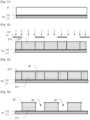
La
L'âme 11 est une plaquette en silicium, mais on peut envisager d'utiliser une plaquette en verre, ou une plaquette en céramique ou même une plaquette métallique. La couche conductrice de base 12 peut comprendre une sous couche de chrome ou de titane ou de tantale et une couche d'or ou de cuivre ou de palladium ou d'argent ou de platine. On peut noter que la couche conductrice de base 12 est optionnelle et peut être omise, en particulier si les pièces métalliques sont à former avec un procédé « electroless » ou par dépôt autocatalytique.The
La résine photosensible 21 vient d'être déposée sur le substrat 10 et forme une couche homogène comme le montre la
On peut déposer la résine photosensible 21 en une ou plusieurs fois, sous forme visqueuse ou liquide, mais on peut également déposer une couche de résine photosensible 21 polymérisée et préparée à l'avance, comme une couche de résine solide (un film sec ou une feuille sèche de résine, à laminer).The
La
Comme le montre la
On peut noter que les parties activées 211 forment des motifs en relief, entourant des cavités 50 qui laissent apparaître la surface conductrice de base de la couche conductrice 12. Les cavités 50 forment typiquement une ou plusieurs empreinte(s) pour réaliser la déposition de métal et former ainsi des pièces métalliques par galvanoplastie et/ou croissance métallique.It can be noted that the activated
On peut noter que l'exemple décrit fait appel à une résine négative, mais on peut envisager d'utiliser une résine positive. De plus, il est possible de déposer, irradier et développer successivement plusieurs couches de résine photosensible pour créer des moule multi niveaux.It can be noted that the example described uses a negative resin, but we can consider using a positive resin. In addition, it is possible to successively deposit, irradiate and develop several layers of photosensitive resin to create multi-level molds.
On peut noter également
De tels résidus 213 sont typiquement un obstacle à l'amorçage homogène de la croissance galvanique ou du dépôt autocatalytique sur toute la surface au fond des cavités 50, ce qui peut entraîner des défauts dans les pièces métalliques formées.
En effet, la
Afin de palier cet inconvénient, il est proposé, à l'issue du développement montré
En particulier, il est proposé d'amorcer la surface en fond des cavités 50, c'est-à-dire à rendre la surface en fond des cavités 50 homogène ou continue (en termes de conductivité électrique, composition, rugosité...) pour démarrer la croissance ou le dépôt métallique de manière uniforme et sans les défauts 411 visibles
La
En particulier, l'étape d'exposition des cavités à un traitement plasma, de préférence un plasma micro-onde, est effectuée :
- pendant un intervalle de temps allant de 10 s à 1 min,
- dans une plage de températures allant de 22°C à 60°C,
- avec un débit allant de 50 sccm (Standard Cubic Centimeters per Minute) à 200 sccm de gaz CF4 et un débit allant de 100 sccm à 600 sccm de gaz O2,
- dans une plage de puissance allant de 100 W à 600 W,
- de préférence dans une cage de faraday.
- for a time interval ranging from 10 s to 1 min,
- in a temperature range from 22°C to 60°C,
- with a flow rate ranging from 50 sccm (Standard Cubic Centimeters per Minute) to 200 sccm of CF 4 gas and a flow rate ranging from 100 sccm to 600 sccm of O 2 gas,
- in a power range from 100 W to 600 W,
- preferably in a faraday cage.
En tout état de cause, le traitement au plasma est ajusté en temps pour retirer les résidus 213 et pas plus. Autrement dit, le traitement au plasma est ajusté pour ne retirer au plus 1 µm de résine photosensible. On peut prévoir par exemple de former les parties activées 211 à des dimensions augmentées d'un micromètre à l'étape d'irradiation de la
Une autre possibilité du premier aspect de l'invention pour former des pièces métalliques exemptes des défauts 411 représentés
Sur la
Le dépôt physique d'or en phase vapeur est ajusté pour juste recouvrir les résidus 213 et/ou pour atteindre la limite de percolation de conduite de courant électrique au fond des cavités 50, et pas sur les flancs ou parois verticale des parties activées 211, afin de ne pas perturber la croissance galvanique en cas de galvanoplastie par électrodéposition. En conséquence, comme le fond des cavités 50 est parfaitement conducteur de l'électricité avec la couche conductrice de recouvrement 13, l'amorçage de la croissance galvanique ou du dépôt autocatalytique de matière métallique se fait de manière uniforme à partir du fond des cavités 50, si bien que les pièces métalliques 41 de la
La
L'âme 11 est une plaquette en silicium, mais on peut envisager d'utiliser une plaquette en verre, ou une plaquette en céramique ou même une plaquette métallique. La couche conductrice de base 12 peut comprendre une sous couche de chrome ou de titane et une couche d'or ou de cuivre.The
On peut noter que la couche conductrice de base 12 est optionnelle et peut être omise.It can be noted that the base
La
En ce qui concerne spécifiquement une couche de résine solide du type lamina (un film de résine sèche), plusieurs épaisseurs de ces films sont proposées dans le commerce et permettent d'éviter une phase de rectification car la planéité et l'épaisseur sont contrôlées. Une épaisseur couramment utilisée est de 150 µm.With regard specifically to a layer of solid resin of the lamina type (a film of dry resin), several thicknesses of these films are offered commercially and make it possible to avoid a rectification phase because the flatness and the thickness are controlled. A commonly used thickness is 150 µm.
La résine photosensible 21 est une résine photosensible négative couramment utilisée dans la fabrication de microsystèmes. Il s'agit d'un polymère très visqueux qui peut être tourné (dépose à la tournette) ou étalé sur une épaisseur allant de 1 micromètre à 2 millimètres. On peut par exemple utiliser une résine SU-8 composée de résine époxyde, de carbonate de propylène, de l'amorceur triaryl-sulfonium et d'un solvant organique (cyclopentanone ou gamma-butyrolactone, selon la formulation). On peut ensuite effectuer un chauffage ou un recuit (« pre-bake ») pour évaporer le ou les solvants et pour solidifier la résine.
On peut déposer la résine photosensible 21 en une ou plusieurs fois, sous forme visqueuse ou liquide ou encore solide (un film sec ou une feuille sèche de résine non réticulée, à laminer), mais on peut également déposer une couche de résine photosensible 21 polymérisée et préparée à l'avance.The
La
Comme le montre la
Au lieu de passer à l'étape de développement de la résine photosensible 21, il est proposé de réaliser un premier traitement thermique à une température comprise entre 25°C et 65°C et de déposer sur la résine photosensible 21 partiellement réticulée une couche solvantée 25 (c'est-à-dire une couche formée par un matériau comprenant au moins un solvant pouvant dissoudre les sels activés ou le polymère activé), comme le montre la
En ce qui concerne spécifiquement la couche de résine solide du type lamina (un film de résine sèche) qui peut être utilisée, le premier traitement thermique est plus court et peut être effectué à plus basse température car il y a peu ou pas de solvant à évaporer. Le procédé de lithographie est raccourci d'une manière importante.Specifically regarding the lamina-type solid resin layer (a dry resin film) that may be used, the first heat treatment is shorter and can be performed at a lower temperature because there is little or no solvent involved. evaporate. The lithography process is shortened significantly.
Le but de ces opérations est de provoquer une migration ou une diffusion des acides photo-initiateurs présents dans les parties activées 211 vers les parties non activées 212, afin d'étendre depuis les parties activées 211 la réticulation de la résine horizontalement et sur une couche proche de la surface.The aim of these operations is to cause a migration or diffusion of the photo-initiator acids present in the activated
D'une manière générale, le premier traitement thermique est effectué pendant une durée allant de 5 min à plusieurs jours pour les plus basses températures. Le premier traitement thermique est effectué préférentiellement de 40 à 60°C de 30 min à 1h. Ce premier traitement thermique a pour effet de provoquer une réticulation plus complète de la résine photosensible 21, pour éviter qu'une trop grande quantité acides photo-initiateurs ne migre vers les parties non activées 212.Generally speaking, the first heat treatment is carried out for a duration ranging from 5 minutes to several days for the lowest temperatures. The first heat treatment is preferably carried out at 40 to 60°C for 30 min to 1 hour. This first heat treatment has the effect of causing a more complete crosslinking of the
En ce qui concerne la couche solvantée 25, celle-ci a pour fonction de provoquer et/ou permettre et/ou véhiculer la migration ou la diffusion des acides photo-initiateurs vers les parties non activées 212. On peut prévoir pour la couche solvantée 25 de simplement déposer de la résine photosensible liquide, ou un gel comprenant un solvant ou un mélange de solvants ou directement un solvant ou un mélange de solvants. Dans le détail, on peut prévoir d'utiliser au moins un premier solvant permettant de dissoudre les sels photosensibles et /ou le polymère activé de la couche épaisse de résine photosensible 21 et un deuxième solvant ne réagissant pas avec le système (pour contrôler et/ou ajuster le pouvoir de dissolution du premier solvant). Ce mélange de solvants dissout de manière contrôlée (et faiblement) les constituants pour permettre une faible migration des constituants en surface des zones exposées et former ainsi un faible rebord. On peut prévoir par exemple un solvant (pouvant dissoudre les sels photosensibles et /ou le polymère activé) choisi parmi : cyclopentanone, PGMEA, acétone ; gamma-butyrolactone ... On peut prévoir par exemple l'Isopropylalcool comme solvant ne réagissant pas.With regard to the
En ce qui concerne les modes de réalisation avec un gel, en particulier pour former un gel ou un mélange visqueux de solvant, on peut par exemple prévoir de dissoudre dans un solvant (ou un mélange de solvant) un polymère ne réagissant pas avec le système, comme par exemple le polyéthylène glycol ou PEG ou encore la polyvinylpyrrolidone (PVP) ... Un mélange visqueux est plus facile à déposer et les moules après dépôt sont plus faciles à manipuler.With regard to the embodiments with a gel, in particular to form a gel or a viscous mixture of solvent, it is possible for example to dissolve in a solvent (or a mixture of solvent) a polymer which does not react with the system. , such as for example polyethylene glycol or PEG or polyvinylpyrrolidone (PVP)... viscous mixture is easier to deposit and the molds after deposit are easier to handle.
En ce qui concerne le deuxième traitement thermique il peut être effectué pendant une durée allant de 5 min à 5h, pour permettre la réticulation des zones des parties non activées 212 qui ont reçu des acides photo-initiateurs. Ainsi, en surface de la résine photosensible 21, les parties activées 211 « débordent » désormais sur les parties non activées 212 avec des rebords 22 qui restent en place après développement comme le montre la
Les rebords 22 de la
- la durée et la température du premier traitement thermique (plus ce dernier sera chaud et long, plus les rebords seront étroits car la migration sera rendue plus difficile),
- la durée laissée entre le premier traitement thermique et le deuxième traitement thermique (plus la couche solvantée sera laissée longtemps sur la résine photosensible 21 avant le deuxième traitement thermique, plus les rebords seront larges),
- la quantité et la nature des solvants utilisés.
- the duration and temperature of the first heat treatment (the hotter and longer the latter, the narrower the edges will be because migration will be made more difficult),
- the duration left between the first heat treatment and the second heat treatment (the longer the solvent layer is left on the
photosensitive resin 21 before the second heat treatment, the wider the edges will be), - the quantity and nature of the solvents used.
Après le deuxième traitement thermique appliqué sur le moule de la
On peut noter que les parties activées 211 munies des rebords 22 forment des motifs en relief, entourant des cavités 50 qui laissent apparaître la couche conductrice de base 12 (qui est optionnelle comme expliqué ci-dessus). Les cavités 50 forment typiquement une ou plusieurs empreinte(s) pour réaliser la déposition de métal et former ainsi des pièces métalliques par galvanoplastie et/ou croissance métallique.It can be noted that the activated
On peut noter que l'exemple décrit fait appel à une résine négative, mais on peut envisager d'utiliser une résine positive. De plus, il est possible de déposer, irradier et développer successivement plusieurs couches de résine photosensible pour créer un moule multi niveaux. Dans ce cas, on peut prévoir de former des rebords 22 sur chaque couche épaisse de résine photosensible, et /ou uniquement sur le haut des structures du dernier niveau.It can be noted that the example described uses a negative resin, but we can consider using a positive resin. In addition, it is possible to successively deposit, irradiate and develop several layers of photosensitive resin to create a multi-level mold. In this case, we can plan to form edges 22 on each thick layer of photosensitive resin, and/or only on the top of the structures of the last level.
Même si dans l'exemple représenté le fond des cavités 50 est normalement formé par la couche conductrice de base 12, cette dernière peut être absente ou recouverte de résidus non conducteurs qui affecteront la croissance galvanique.Even if in the example shown the bottom of the
La
Selon un mode de réalisation, l'étape de formation d'une couche conductrice de recouvrement 13 au fond des cavités 50 peut être effectuée :
- sous niveau de vide inférieur à 10-4 mbar, et de préférence inférieur à 10-6 mbar,
- en plaçant par exemple une plaquette de 150 mm de côté ou de diamètre formant le substrat à au moins 500 mm de la source de matière à vaporiser et de préférence à au moins 700 mm de la source de matière à vaporiser, et/ou en chauffant la source de matière à vaporiser juste au dessus de sa température de fusion,
- en utilisant une source métallique pure à 99% au moins, comme par exemple une source d'or pur à 99% en poids.
- under vacuum level less than 10 -4 mbar, and preferably less than 10 -6 mbar,
- by placing for example a plate of 150 mm side or diameter forming the substrate at least 500 mm from the source of material to be vaporized and preferably at least 700 mm from the source of material to be vaporized, and/or by heating the source of material to be vaporized just above its melting temperature,
- using a metallic source that is at least 99% pure, such as for example a source of gold that is 99% pure by weight.
Une telle couche conductrice de recouvrement 13 a pour effet de permettre une croissance homogène depuis toute la surface inférieure, si le substrat 10 est exempt de de couche conductrice de base 12, ou pour garantir une croissance homogène si la couche conductrice de base 12 est présente mais recouverte par endroits ou en totalité par des résidus. Lors de cette étape de dépôt physique en phase vapeur, qui est directionnel (selon la direction verticale de la
On peut noter que juste avant d'effectuer le dépôt physique par phase vapeur d'or des
La
Lors d'un dépôt physique par phase vapeur directionnel, effectué sur une plaquette de 150 mm de diamètre, la plaquette étant disposée à 70 cm de la source de matière à déposer (la cible), on peut considérer qu'on dépose environ 10 fois moins de matière sur les flancs verticaux du moule qu'au fond des cavités (en particulier pour les parties excentrées du moule, agencées en périphérie). Ainsi, avec une épaisseur totale en fond de cavité comprise entre 3 nm et 8 nm (par exemple 1 à 3 nm, par exemple 2 nm de chrome et 2 à 5 nm, par exemple 3 nm d'or), dans la zone où la résistance électrique commence à décroître plus lentement sur la
Un procédé de fabrication de moule selon la présente invention, et l'utilisation de ces moules pour former des pièces métalliques, sont susceptibles d'application industrielle.A mold manufacturing method according to the present invention, and the use of these molds to form metal parts, are capable of industrial application.
On comprendra que diverses modifications et/ou améliorations évidentes pour l'homme du métier peuvent être apportées aux différents modes de réalisation de l'invention décrits dans la présente description sans sortir du cadre de l'invention.It will be understood that various modifications and/or improvements obvious to those skilled in the art can be made to the different embodiments of the invention described in the present description without departing from the scope of the invention.
Claims (13)
Applications Claiming Priority (1)
| Application Number | Priority Date | Filing Date | Title |
|---|---|---|---|
| EP22200410.3A EP4350436A1 (en) | 2022-10-07 | 2022-10-07 | Method for manufacturing mold for forming metal part by metal growth |
Publications (1)
| Publication Number | Publication Date |
|---|---|
| EP4350438A1 true EP4350438A1 (en) | 2024-04-10 |
Family
ID=83689218
Family Applications (2)
| Application Number | Title | Priority Date | Filing Date |
|---|---|---|---|
| EP22200410.3A Pending EP4350436A1 (en) | 2022-10-07 | 2022-10-07 | Method for manufacturing mold for forming metal part by metal growth |
| EP23202044.6A Pending EP4350438A1 (en) | 2022-10-07 | 2023-10-06 | Method for manufacturing mold for forming metal part by metal growth |
Family Applications Before (1)
| Application Number | Title | Priority Date | Filing Date |
|---|---|---|---|
| EP22200410.3A Pending EP4350436A1 (en) | 2022-10-07 | 2022-10-07 | Method for manufacturing mold for forming metal part by metal growth |
Country Status (1)
| Country | Link |
|---|---|
| EP (2) | EP4350436A1 (en) |
Citations (4)
| Publication number | Priority date | Publication date | Assignee | Title |
|---|---|---|---|---|
| EP1835339A1 (en) | 2006-03-15 | 2007-09-19 | Doniar S.A. | Fabrication process by LIGA type technology, of a monolayer or multilayer metallic structure, and structure obtained therewith |
| EP3454122A1 (en) * | 2017-09-11 | 2019-03-13 | Patek Philippe SA Genève | Method for manufacturing a metal microstructure using liga technology, comprising at least two levels |
| EP3547027A1 (en) * | 2018-03-29 | 2019-10-02 | Mimotec S.A. | Method for manufacturing a multi-level micromould for electroforming micromechanical components and micromould obtained by the method |
| EP3839627A1 (en) * | 2019-12-18 | 2021-06-23 | Mimotec S.A. | Method for manufacturing a micromould for electroforming of micromechanical components |
Family Cites Families (4)
| Publication number | Priority date | Publication date | Assignee | Title |
|---|---|---|---|---|
| US5158860A (en) * | 1990-11-01 | 1992-10-27 | Shipley Company Inc. | Selective metallization process |
| US5925501A (en) * | 1997-12-15 | 1999-07-20 | Chartered Semiconductor Manufacturing Ltd | Dark CF4 flash |
| US6207583B1 (en) * | 1998-09-04 | 2001-03-27 | Alliedsignal Inc. | Photoresist ashing process for organic and inorganic polymer dielectric materials |
| US6693043B1 (en) * | 2002-09-20 | 2004-02-17 | Novellus Systems, Inc. | Method for removing photoresist from low-k films in a downstream plasma system |
-
2022
- 2022-10-07 EP EP22200410.3A patent/EP4350436A1/en active Pending
-
2023
- 2023-10-06 EP EP23202044.6A patent/EP4350438A1/en active Pending
Patent Citations (4)
| Publication number | Priority date | Publication date | Assignee | Title |
|---|---|---|---|---|
| EP1835339A1 (en) | 2006-03-15 | 2007-09-19 | Doniar S.A. | Fabrication process by LIGA type technology, of a monolayer or multilayer metallic structure, and structure obtained therewith |
| EP3454122A1 (en) * | 2017-09-11 | 2019-03-13 | Patek Philippe SA Genève | Method for manufacturing a metal microstructure using liga technology, comprising at least two levels |
| EP3547027A1 (en) * | 2018-03-29 | 2019-10-02 | Mimotec S.A. | Method for manufacturing a multi-level micromould for electroforming micromechanical components and micromould obtained by the method |
| EP3839627A1 (en) * | 2019-12-18 | 2021-06-23 | Mimotec S.A. | Method for manufacturing a micromould for electroforming of micromechanical components |
Also Published As
| Publication number | Publication date |
|---|---|
| EP4350436A1 (en) | 2024-04-10 |
Similar Documents
| Publication | Publication Date | Title |
|---|---|---|
| EP2316056B1 (en) | Process for fabricating multi-level metal parts by the uv-liga technique | |
| EP2229470B1 (en) | Method for obtaining a metal microstructure and microstructure obtained according to said method | |
| EP2004881B1 (en) | Process for the fabrication of liga-uv multilayer metallic structures, the layers being adjacent and not completely superimposed, and structure therefrom. | |
| FR2477472A1 (en) | INK JET HEAD AND METHOD FOR MANUFACTURING THE SAME | |
| EP0184567A1 (en) | Process for the formation of negative patterns in a photoresist layer | |
| WO2016102628A1 (en) | Method for producing patterns | |
| EP3839624B1 (en) | Method for manufacturing a timepiece component | |
| FR2472213A1 (en) | FABRICATION OF CIRCUIT MICROMINIATURE IN THE STATE SOLID AND CIRCUITS SO OBTAINED | |
| EP4350438A1 (en) | Method for manufacturing mold for forming metal part by metal growth | |
| EP3454122B1 (en) | Method for manufacturing a metal microstructure using liga technology, comprising at least two levels | |
| EP3802920B1 (en) | Method for producing a metal decoration on a dial and dial obtained according to said method | |
| FR2596921A1 (en) | METHOD OF FORMING A CONDUCTIVE DESIGN ON THE SURFACE OF A SEMICONDUCTOR AS IN PARTICULAR SILICON, GERMANIUM AND GALLIUM ARSENIUM | |
| EP3602196A1 (en) | Method for manufacturing a timekeeping component and component obtained by the method | |
| EP3495894A1 (en) | Method for manufacturing a clock component | |
| EP4350443A1 (en) | Mould for forming metal parts by metal growth and method for manufacturing such a mould | |
| EP1576420B8 (en) | Nano-imprint lithography method involving substrate pressing | |
| EP4350437A1 (en) | Method for manufacturing a mould for forming metal parts by metal growth | |
| CH699416A2 (en) | Fabricating multi-level metallic e.g. steel microstructure by UV photolithography and galvanic deposition, comprises covering conductive surface of substrate by first layer of photosensitive resin, and irradiating first layer through mask | |
| EP1759165A1 (en) | Calibrating device on a silicon substrate | |
| EP3840019B1 (en) | Method for forming a porous portion in a substrate | |
| EP3841433B1 (en) | Method for manufacturing a timepiece component and component produced by this method | |
| FR2809532A1 (en) | Simplified method for the photoengraving of photosensitive material allowing simultaneous double face treatment of a semiconductor substrate | |
| CA2409232A1 (en) | Process for the manufacture of an electronic component containing an inductive micro-component | |
| EP3555706B1 (en) | Method for functionalising a substrate | |
| CH716967A2 (en) | A method of manufacturing a watch component and a component obtained according to this method. |
Legal Events
| Date | Code | Title | Description |
|---|---|---|---|
| PUAI | Public reference made under article 153(3) epc to a published international application that has entered the european phase |
Free format text: ORIGINAL CODE: 0009012 |
|
| STAA | Information on the status of an ep patent application or granted ep patent |
Free format text: STATUS: THE APPLICATION HAS BEEN PUBLISHED |
|
| AK | Designated contracting states |
Kind code of ref document: A1 Designated state(s): AL AT BE BG CH CY CZ DE DK EE ES FI FR GB GR HR HU IE IS IT LI LT LU LV MC ME MK MT NL NO PL PT RO RS SE SI SK SM TR |