EP1833129B1 - Laseranordnung mit integrierter Fotodiode - Google Patents
Laseranordnung mit integrierter Fotodiode Download PDFInfo
- Publication number
- EP1833129B1 EP1833129B1 EP06256293.9A EP06256293A EP1833129B1 EP 1833129 B1 EP1833129 B1 EP 1833129B1 EP 06256293 A EP06256293 A EP 06256293A EP 1833129 B1 EP1833129 B1 EP 1833129B1
- Authority
- EP
- European Patent Office
- Prior art keywords
- substrate
- doped region
- semiconductor laser
- sel
- laser
- Prior art date
- Legal status (The legal status is an assumption and is not a legal conclusion. Google has not performed a legal analysis and makes no representation as to the accuracy of the status listed.)
- Not-in-force
Links
Images



Classifications
-
- H—ELECTRICITY
- H01—ELECTRIC ELEMENTS
- H01S—DEVICES USING THE PROCESS OF LIGHT AMPLIFICATION BY STIMULATED EMISSION OF RADIATION [LASER] TO AMPLIFY OR GENERATE LIGHT; DEVICES USING STIMULATED EMISSION OF ELECTROMAGNETIC RADIATION IN WAVE RANGES OTHER THAN OPTICAL
- H01S5/00—Semiconductor lasers
- H01S5/02—Structural details or components not essential to laser action
- H01S5/026—Monolithically integrated components, e.g. waveguides, monitoring photo-detectors, drivers
- H01S5/0262—Photo-diodes, e.g. transceiver devices, bidirectional devices
- H01S5/0264—Photo-diodes, e.g. transceiver devices, bidirectional devices for monitoring the laser-output
-
- H—ELECTRICITY
- H01—ELECTRIC ELEMENTS
- H01S—DEVICES USING THE PROCESS OF LIGHT AMPLIFICATION BY STIMULATED EMISSION OF RADIATION [LASER] TO AMPLIFY OR GENERATE LIGHT; DEVICES USING STIMULATED EMISSION OF ELECTROMAGNETIC RADIATION IN WAVE RANGES OTHER THAN OPTICAL
- H01S5/00—Semiconductor lasers
-
- H—ELECTRICITY
- H01—ELECTRIC ELEMENTS
- H01S—DEVICES USING THE PROCESS OF LIGHT AMPLIFICATION BY STIMULATED EMISSION OF RADIATION [LASER] TO AMPLIFY OR GENERATE LIGHT; DEVICES USING STIMULATED EMISSION OF ELECTROMAGNETIC RADIATION IN WAVE RANGES OTHER THAN OPTICAL
- H01S3/00—Lasers, i.e. devices using stimulated emission of electromagnetic radiation in the infrared, visible or ultraviolet wave range
- H01S3/09—Processes or apparatus for excitation, e.g. pumping
- H01S3/091—Processes or apparatus for excitation, e.g. pumping using optical pumping
- H01S3/094—Processes or apparatus for excitation, e.g. pumping using optical pumping by coherent light
- H01S3/0941—Processes or apparatus for excitation, e.g. pumping using optical pumping by coherent light of a laser diode
-
- H—ELECTRICITY
- H01—ELECTRIC ELEMENTS
- H01S—DEVICES USING THE PROCESS OF LIGHT AMPLIFICATION BY STIMULATED EMISSION OF RADIATION [LASER] TO AMPLIFY OR GENERATE LIGHT; DEVICES USING STIMULATED EMISSION OF ELECTROMAGNETIC RADIATION IN WAVE RANGES OTHER THAN OPTICAL
- H01S5/00—Semiconductor lasers
- H01S5/06—Arrangements for controlling the laser output parameters, e.g. by operating on the active medium
- H01S5/068—Stabilisation of laser output parameters
- H01S5/0683—Stabilisation of laser output parameters by monitoring the optical output parameters
-
- H—ELECTRICITY
- H01—ELECTRIC ELEMENTS
- H01S—DEVICES USING THE PROCESS OF LIGHT AMPLIFICATION BY STIMULATED EMISSION OF RADIATION [LASER] TO AMPLIFY OR GENERATE LIGHT; DEVICES USING STIMULATED EMISSION OF ELECTROMAGNETIC RADIATION IN WAVE RANGES OTHER THAN OPTICAL
- H01S5/00—Semiconductor lasers
- H01S5/10—Construction or shape of the optical resonator, e.g. extended or external cavity, coupled cavities, bent-guide, varying width, thickness or composition of the active region
- H01S5/18—Surface-emitting [SE] lasers, e.g. having both horizontal and vertical cavities
- H01S5/183—Surface-emitting [SE] lasers, e.g. having both horizontal and vertical cavities having only vertical cavities, e.g. vertical cavity surface-emitting lasers [VCSEL]
-
- H—ELECTRICITY
- H01—ELECTRIC ELEMENTS
- H01S—DEVICES USING THE PROCESS OF LIGHT AMPLIFICATION BY STIMULATED EMISSION OF RADIATION [LASER] TO AMPLIFY OR GENERATE LIGHT; DEVICES USING STIMULATED EMISSION OF ELECTROMAGNETIC RADIATION IN WAVE RANGES OTHER THAN OPTICAL
- H01S5/00—Semiconductor lasers
- H01S5/02—Structural details or components not essential to laser action
- H01S5/022—Mountings; Housings
- H01S5/0233—Mounting configuration of laser chips
- H01S5/02345—Wire-bonding
Definitions
- This invention relates generally to semiconductor lasers, and, more particularly, to assemblies comprising surface-emitting lasers.
- Semiconductor lasers are typically fabricated on semiconductor wafers before they are cleaved into discrete laser devices.
- Semiconductor lasers maybe edge-emitting lasers (EELs) or surface-emitting lasers (SELs).
- EELs edge-emitting lasers
- SELs surface-emitting lasers
- a SEL usually comprises an active region with one or more quantum wells for light generation. This active region, in turn, is sandwiched between upper and lower distributed Bragg reflector (DBR) mirrors.
- DBR distributed Bragg reflector
- the DBR mirrors are constructed from a combination of semiconductor and dielectric layers with differing refractive indices.
- the upper DBR mirror typically has a lower reflectivity than the lower DBR mirror and is, therefore, the exit mirror through which the primary light output of the SEL is emitted.
- SELs have various advantages over EELs for some applications including telecommunications and optical storage.
- a SEL typically has light output that is more circular and has a smaller divergence angle than the light output generated by an EEL.
- SELs may also be less costly to produce and more energy efficient.
- SELS are easier to test during manufacturing than EELs. This is due to the fact that EELs, unlike SELS, cannot be tested when they are still incorporated in a semiconductor wafer because of the parallel direction of light output.
- the output power of a semiconductor laser is critically dependent on the operating temperature of that laser.
- automatic power control feedback methods are frequently implemented when using a semiconductor laser in order to maintain the laser's output power at a constant target value as the laser changes temperature.
- Automatic power control of a semiconductor laser is usually achieved by monitoring the output power of the laser using a monitor photodiode.
- the monitor photodiode generates an electrical output signal that is communicated to control circuitry external to the laser assembly.
- the control circuitry determines the appropriate drive power that should be supplied to the laser in order to maintain the laser's output power at the constant target value.
- US 5 258 991 discloses a monolithic laser diode and monitor photodetector.
- a dielectric coating deposited simultaneously on the output facet of the laser diode.
- the photodetector is placed at a tilt angle, within a predetermined range of tilt angles, with respect to the laser diode back facet.
- the predetermined range of tilt angles is selected according to the thickness and refractive index of the dielectric coating.
- EP 0 410 067 discloses an integrated semiconductor structure with optically coupled laser diode and photodiode, both having etched, vertical facets.
- the photodiode has a spatially non-uniform sensitivity profile with respect to the incident light beam emitted by the laser. This is due to the varying distance from the laser facet and/or to variations in the angle of incidence and results in photocurrents produced by the photodiode that depend on the intensity distribution of the light beam.
- the spatially non-uniform sensitivity profile allows the measurement of the far-field intensity distribution of the laser and thus on-wafer screening of lasers with respect to their mode-stability.
- US 6 005 262 discloses a laser assembly in which an anti-reflection coating, preferably constructed of dull material such as aluminium, is formed above a detector. The coating prevents undesirable feedback of rearwardly emitted light into a VCSEL.
- US 2005/189473 relates to an arrangement having at least one laser diode and a monitor component operatively coupled to the laser diode to detect at least some radiation radiated by the emission component.
- the monitor component is integrated into the carrier substrate and may be a photodiode including a pn junction.
- Embodiments of the present invention address the above-identified need by providing assemblies for use in applications involving SELs. These assemblies utilize a substrate with an integrated photodiode for automatic power control. The photodiode monitors the secondary light output that is transmitted through the lower DBR mirror of the SEL. In this way, the primary light output of the SEL is not involved in the automatic power control.
- a laser assembly comprises a substrate, one or more standoffs and a semiconductor laser.
- the substrate has a first doped region and a second doped region.
- the second doped region is proximate to an upper surface of the substrate and forms a pn junction with the first doped region.
- the semiconductor laser is operative to emit light from an upper surface and a lower surface.
- the semiconductor laser is attached to the upper surface of the substrate with the one or more standoffs such that the light emitted from the lower surface of the semiconductor laser impinges on the second doped region.
- a groove is formed in the upper surface of the substrate in the second doped region, the groove having at least first and second sloped surfaces.
- the light emitted from the lower surface of the semiconductor laser and impinging on the second doped region impinges on one or more of the sloped surfaces of the groove.
- a portion of the light emitted from the lower surface of the semiconductor laser is steered away from the portion of the lower surface of the semiconductor where the light was emitted.
- the assembly comprises an n-doped silicon substrate with a p-doped region proximate to an upper surface of the substrate. These n-doped and p-doped regions form a photosensitive pn junction.
- a SEL is mounted to the upper surface of the substrate with three metallic standoffs and is powered by external control circuitry. The SEL emits its primary light output from its upper surface but also emits secondary light from its lower surface. The light emitted from the lower surface of the SEL impinges on the the sloped surfaces of the groove causes current to flow in the pn junction. This current is fed back to the control circuitry which utilizes the current to maintain the SEL at a target output power.
- automatic power control is thereby achieved by utilizing the secondary light output from the lower surface of the SEL. Issues associated with using the primary light output for automatic power control are thereby avoided by utilizing an assembly in accordance with aspects of the invention.
- standoff' as used herein is intended to encompass any physical structure suitable for separating two physical elements from one another.
- FIG. 1A shows a plan view of an assembly 100.
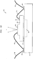
- FIG. 1B shows a sectional view of the FIG. 1A assembly cut in a plane indicated in FIG. 1A .
- the assembly 100 comprises a SEL 105 and a substrate 110.
- the SEL is attached to the substrate by three standoffs, represented by standoff 115.
- a diffusion region 120 Built into the substrate is a diffusion region 120.
- Diffusion contact 125 is attached to this diffusion region.
- a substrate contact 130 is attached to the substrate outside the diffusion region.
- First and second SEL contacts, 135 and 140, respectively, are attached to the SEL.
- the first SEL contact defines a window that allows light to be emitted from the upper surface of the SEL.
- Elements within the assembly 100 are electrically connected to control circuitry 145 that is external to the assembly. These electrical connections are achieved by utilizing various bond pads and wires designed for this purpose. Electrical connections between the control circuitry and the first SEL contact 135 is achieved by electrically connecting the control circuitry to first SEL bond pad 150 using first external SEL wire 155. The first SEL bond pad is, in turn, electrically connected to the first SEL contact via first internal SEL wire 160. In a similar way, the control circuitry is connected to the second SEL contact 140 via second SEL bond pad 165, second external SEL wire 170 and second internal SEL wire 175. Moreover, the control circuitry is attached to the diffusion contact 125 via diffusion bond pad 180, external diffusion wire 185 and internal diffusion wire 190. The substrate contact 130 is accessed by the control circuitry via substrate wire 195.
- the substrate 110 in the assembly 100 preferably comprises n-type silicon.
- the bond pads, contacts and wires preferably comprise a conductive metal such as, but not limited to, aluminum, copper or silver.
- the first SEL bond pad 150, second SEL bond pad 165 and diffusion bond pad 180 each overlie a layer of dielectric material. In this way, these bond pads do not make electrical contact with the substrate.
- the diffusion region 120 can be formed in the substrate 110 using conventional semiconductor processing techniques.
- Forming the diffusion region may comprise, for example, ion implanting impurities into the substrate and then annealing the substrate.
- the annealing step causes the impurities to migrate into the substrate and to become electrically active.
- Both processing steps will be familiar to one skilled in the art and are described in detail in a number of references, including, for example, S. Wolf et al., Silicon Processing for the VLSI Era, Volume 1 - Process Technology, Lattice Press, 1986 , which is incorporated herein by reference.
- FIG. 1C A block diagram of the electrical connections between elements of the assembly 100 and the control circuitry 145 is shown in FIG. 1C .
- the signal pathways in the block diagram are labeled with reference numerals that correspond to their physical implementation (i.e., physical wiring) in FIGS. 1A and 1B .
- SELs are described in detail in a number of readily available references including, for example, C.W. Wilmsen et al., Vertical-Cavity Surface Emitting Lasers: Design, Fabrication, Characterization, and Applications, Cambridge University Press, 1999 , which is incorporated herein by reference.
- the SEL 105 comprises an active region sandwiched between upper and lower DBR mirrors.
- the SEL is powered by applying an electrical voltage across the active region, which, in turn, causes current to flow therein. Electrons in the active region attain high energy states as result of this applied voltage. When the electrons spontaneously drop in energy state, photons are produced. Some of these photons travel in a direction perpendicular to the reflective planes of the DBR mirrors. As a result of the ensuing reflections, these photons travel back and forth through the active region several times. When the photons interact with other high energy state electrons, stimulated emission occurs so that additional photons with similar characteristics are produced.
- the output power of the SEL 105 may, therefore, be modified by changing the voltage across the active region of the SEL.
- the control circuitry 145 applies this voltage to the SEL through the first and second SEL contacts 135, 140.
- the upper and lower DBR mirrors are formed with slightly different reflectivities.
- the upper DBR mirror has a lower reflectivity than the lower DBR mirror.
- the primary light output of the SEL is, therefore, from the upper surface of the SEL (i.e., that surface farthest away from the substrate 110). Nevertheless, a smaller amount of secondary light is also emitted from the lower surface of the SEL (i.e., that surface nearest the substrate).
- the fraction of light emitted from the lower surface of the SEL is proportional to the light emitted from the upper surface.
- the output power of the light emitted from the lower surface of the SEL becomes an ideal source of feedback for controlling the primary output power of the SEL.
- the secondary light emitted from the lower surface of the SEL 105 directly impinges on the diffusion region 120.
- a pn junction is formed.
- this pn junction will act as a photodiode capable of converting the impinging light into a current signal, the magnitude of which is a function of the intensity of the impinging light.
- the design and operating characteristics of photodiodes formed with pn junctions are widely understood and will be familiar to one skilled in the art. Moreover, such devices are described in a number of references, including C. Davis, Lasers and Electro-Optics: Fundamentals and Engineering, Cambridge University Press, 1996 , which is incorporated herein by reference.
- the diffusion region 120 is doped so that it is p-type while the remainder of the substrate 110 is n-type.
- the light emitted from the lower surface of the SEL 105 impinges on the diffusion region and produces a current in the photodiode as a result of the photovoltaic effect. This current, in turn, is transmitted to the control circuitry 145 through the electrical connections shown on FIGS. 1A-1C .
- Silicon-based photodiode arrangements like that in the assembly 100 are typically capable of measuring light intensity for laser light with a wavelength between about 100 and about 1,100 nanometers.
- the control circuitry 145 can act to apply a voltage difference between the diffusion region 120 and the substrate 110, allowing the pn junction to be reverse biased. Reverse biasing the pn junction can make the photodiode more sensitive to light. A reverse biased pn junction also tends to respond more linearly to changes in light intensity.
- Automatic power control of the SEL 105 in the assembly 100 is established by forming an electronic feedback loop between the SEL, the photodiode comprising the diffusion region 120 and the substrate 110, and the control circuitry 145.
- the photodiode transmits current, the magnitude of which is a function of the present light output power of the SEL, to the control circuitry.
- This current is then compared to a predetermined set-point operating current that would be produced by the photodiode if the SEL were producing a target output power.
- the comparison produces an error signal proportional to the difference in the actual SEL output power and the target output power.
- the control circuitry modifies the applied voltage on the SEL in proportion to this error signal.
- the control circuitry decreases the applied voltage on the active region of the SEL so that stimulated emission within the active region is reduced. If, on the other hand, the SEL is operating at a lower output power than the target output power, the control circuitry increases the voltage acting on the active region and stimulated emission is increased. In this way, the control circuitry maintains the SEL at the target output power.
- automatic power control is thereby achieved by utilizing the secondary light output from the lower surface of the SEL 105. Issues associated with using the primary light output for automatic power control are thereby avoided by utilizing an assembly in accordance with aspects of the invention.
- the SEL 105 is attached to the upper surface of the substrate 110 with standoffs 115.
- the standoffs are operative to physically attach the SEL to the substrate.
- the standoffs may serve to transfer heat generated by the SEL to the substrate as a means of dissipating heat from the SEL.
- three rectangular standoffs 115 are utilized to attach the SEL 105 to the upper surface of the substrate 110.
- this standoff design is entirely illustrative and other arrangements may be utilized.
- This single standoff could, for example, have a u-shaped cross-section in the plane parallel to the upper surface of the substrate.
- four standoffs with circular cross-sections in the plane parallel to the upper surface of the substrate may be utilized. These circular standoffs may, for example, be placed proximate to the four corners of the SEL.
- the standoffs 115 will preferably comprise one or more metallic materials, although suitable non-metallic materials may also be utilized.
- Metallic materials have the advantages of providing good thermal conduction between the SEL 105 and the substrate 110, while also being easily fabricated on the substrate and easily bonded to the SEL.
- the standoffs may be formed, for example, by depositing blanket layers of titanium, gold, platinum and gold-tin on the substrate. These layers are then patterned by photolithography and reactive ion etching (RIE) steps to form the three standoffs shown in FIG. 1B .
- RIE reactive ion etching
- Such lithography and RIE steps are conventionally used in semiconductor processing to pattern metallic features and will be familiar to one skilled in the art. They are also described in readily available references, such as the reference by S. Wolf et al. mentioned above and incorporated herein by reference.
- the standoffs may also be formed by other metal deposition techniques, such as, but not limited to, e-beam evaporation.
- those regions of the lower surface of the SEL that will be bonded to the standoffs are also coated with a metallic material such as gold.
- the SEL may then be attached to the standoffs by pressing the SEL to the standoffs while heating the assembly. After achieving a sufficiently high temperature, the gold-tin layer in the standoffs will melt and form a metallic bond with the bonding regions of the SEL. When the temperature is subsequently reduced, this metallic bond will act to hold the SEL to the standoffs.
- a groove is formed in the diffusion region 120 to reduce the back-reflection of light into the SEL 105.
- FIG. 1D shows the assembly 100 with the addition of groove 122 to the diffusion region.
- the groove is preferably defined by four surfaces and has a wedge-shaped cross-section in the plane shown in the figure.
- the wedge-shaped groove is located such that the light emitted from the lower surface of the SEL falls on one of the angled surfaces of the groove. When the light strikes this angled surface, a portion of the light is reflected at an angle equal to the angle of incidence and, as a result, is steered away from the portion of the lower surface of the SEL where the light was emitted.
- this light does not reenter the SEL but is still measured by the photodiode.
- Formation of the groove 122 in the diffusion region 120 can be performed before or after forming the diffusion region in the substrate 110. Formation of the groove is preferably accomplished by conventional photolithography and wet etching steps. To achieve the desired shape, the wet etch is configured such that the rate of chemical etching is highly sensitive to the crystal orientation of the substrate being etched (i.e., the wet etch is anisotropic). If the substrate is made of silicon, for example, such an anisotropic wet etch can be achieved by using a combination of potassium hydroxide, isopropyl alcohol and water.
- FIG. 2 shows a plan view of a multi-laser assembly.
- the assembly 200 comprises three SEL modules 201-1, 201-2 and 201-3.
- Each SEL module contains substantially the same elements as the assembly 100 shown in FIGS. 1A and 1B , and these elements are therefore labeled with the same reference numerals.
- the separate wiring for each SEL module allows the control circuitry to provide independent automatic power control for each SEL in a way similar to that described above.
- the SELs in a multi-laser assembly such as assembly 200 may emit light at the same wavelength or may emit light at different wavelengths, or a combination thereof. Where multiple SELs of the same wavelength are incorporated into a single assembly, simple arrangements of optics may be utilized to combine the primary outputs of the multiple SELs into a single laser beam. This single laser beam will have the combined power of the multiple SELs.
- a multi-laser assembly like the assembly 200 may also be useful in an optical storage drive capable of recording and playing back data in accordance with several optical disc formats such as Blu-ray, DVD and CD. Such a multi-laser assembly would utilize SELs that emit light at different wavelengths from each other.
- Blu-ray is a relatively new optical disc format capable of recording and playing back high-definition content from, for instance, high definition broadcasting.
- Semiconductor lasers for Blu-ray application typically emit at a wavelength of 405 nanometers.
- Semiconductor lasers for DVD and CD applications typically emit at wavelengths of 660 and 785 nanometers, respectively.
Landscapes
- Physics & Mathematics (AREA)
- Electromagnetism (AREA)
- Optics & Photonics (AREA)
- Condensed Matter Physics & Semiconductors (AREA)
- General Physics & Mathematics (AREA)
- Engineering & Computer Science (AREA)
- Plasma & Fusion (AREA)
- Semiconductor Lasers (AREA)
Claims (8)
- Eine Laserbaugruppe (100) aufweisend:ein Substrat (110), wobei das Substrat einen ersten dotierten Bereich und einen zweiten dotierten Bereich (120) hat, wobei der zweite dotierten Bereich naheliegend zu einer oberen Oberfläche des Substrats ist und einen pn Übergang mit dem ersten dotierten Bereich bildet;einen oder mehrere Abstandshalter (115); undeinen Halbleiter Laser (105), wobei der Halbleiter Laserfunktionsfähig ist zum Emittieren von Licht von einer oberen Oberfläche und einer unteren Oberfläche undan der oberen Oberfläche des Substrats mit dem einen oder den mehreren Abstandshaltern derartig befestigt ist, dass das Licht, welches von der unteren Oberfläche des Halbleiter Lasers emittiert wird, auf den zweiten dotierten Bereich (120) auftrifft,wobei der pn Übergang konfiguriert ist, als eine Photodiode zum Konvertieren des auftretenden Lichts zu wirken, welches von der unteren Oberfläche des Halbleiter Lasers (105) emittiert wird, in ein Stromsignal;
dadurch gekennzeichnet, dasseine Nut (122) in der oberen Oberfläche des Substrats (110) in dem zweiten dotierten Bereich (120) gebildet ist, wobei die Nut zumindest eine erste und eine zweite geneigte Oberfläche hat; unddas Licht, welches von der unteren Oberfläche des Halbleiter Lasers emittiert wird und auf den zweiten dotierten Bereich auftrifft, auf eine oder mehrere der geneigten Oberflächen der Nut auftrifft, wobei ein Teil des Lichts, welches von der unteren Oberfläche des Halbleiter Lasers emittiert wird, von dem Teil der unteren Oberfläche des Halbleiters weg gelenkt wird, wo das Licht emittiert wurde. - Die Laserbaugruppe gemäß Anspruch 1, wobei der Halbleiter Laser einen Oberflächen-emittierenden Laser aufweist.
- Die Laserbaugruppe gemäß Anspruch 1, wobei der pn Übergang Strom erzeugt, dessen Stärke eine Funktion der Ausgangsleistung des Halbleiter Lasers ist.
- Die Laserbaugruppe gemäß Anspruch 1, wobei die Nut einen Querschnitt hat, welcher im Wesentlichen keilförmig in einer Ebene ist, welche senkrecht zu der Ebene liegt, die mittels der oberen Oberfläche des Substrats definiert ist.
- Die Laserbaugruppe gemäß Anspruch 1, ferner aufweisend:einen dritten dotierten Bereich in dem Substrat, wobei der dritte dotierte Bereich naheliegend zu der oberen Oberfläche des Substrats ist und einen pn Übergang mit dem ersten dotierten Bereich bildet; undeinen zweiten Halbleiter Laser, wobei der zweite Halbleiter Laserfunktionsfähig ist zum Emittieren von Licht von einer oberen Oberfläche und einer unteren Oberfläche undan der oberen Oberfläche des Substrats mit einem oder mehreren Abstandshaltern derartig befestigt ist, dass das Licht, welches von der unteren Oberfläche des Halbleiter Lasers emittiert wird, auf den dritten dotierten Bereich auftrifft.
- Eine Vorrichtung aufweisend:eine Laser Baugruppe (100) gemäß irgendeinem der Ansprüche 1 bis 5, undeinen Steuerschaltkreis (145), wobei der Steuerschaltkreis funktionsfähig ist zum Steuern einer Ausgangsleistung des Halbleiter Lasers als Reaktion auf Strom, welcher mittels der Photodiode erzeugt wird;
dadurch gekennzeichnet, dasseine Nut (122) in der oberen Oberfläche des Substrats in dem zweiten dotierten Bereich gebildet ist, wobei die Nut zumindest eine erste und eine zweite geneigte Oberfläche hat; unddas Licht, welches von der unteren Oberfläche des Halbleiter Lasers emittiert wird und auf den zweiten dotierten Bereich auftrifft, auf eine oder mehrere der geneigten Oberflächen der Nut auftrifft, wobei ein Teil des Lichts, welches von der unteren Oberfläche des Halbleiter Lasers emittiert wird, von dem Teil der unteren Oberfläche des Halbleiters weg gelenkt wird, wo das Licht emittiert wurde. - Die Vorrichtung gemäß Anspruch 6, wobei der Steuerschaltkreis funktionsfähig ist zum Aufrechterhalten der Ausgangsleistung des Halbleiter Lasers bei einem vorbestimmten Wert.
- Ein Verfahren zum Bilden einer Laserbaugruppe (100), wobei das Verfahren die Schritte aufweist:Bilden eines Substrats (110), wobei das Substrat einen ersten dotierten Bereich und einen zweiten dotierten Bereich (120) hat, wobei der zweite dotierte Bereich naheliegend zu einer oberen Oberfläche des Substrats ist und einen pn Übergang mit dem ersten dotierten Bereich bildet; undBefestigen eines Halbleiter Lasers (105), welcher funktionsfähig ist zum Emittieren von Licht von einer oberen Oberfläche und einer unteren Oberfläche, an der oberen Oberfläche des Substrats mit einem oder mehreren Abstandshaltern (115), derartig dass das Licht, welches von der unteren Oberfläche des Halbleiter Lasers emittiert wird, auf den zweiten dotierten Bereich auftrifft,Konfigurieren des pn Übergangs, als eine Photodiode zum Konvertieren des auftretenden Lichts zu wirken, welches von der unteren Oberfläche des Halbleiter Lasers (105) emittiert wird, in ein Stromsignal;
dadurch gekennzeichnet, dasseine Nut (122) in der oberen Oberfläche des Substrats in dem zweiten dotierten Bereich gebildet wird, wobei die Nut zumindest eine erste und eine zweite geneigte Oberfläche hat; unddas Licht, welches von der unteren Oberfläche des Halbleiter Lasers emittiert wird und auf den zweiten dotierten Bereich auftrifft, auf eine oder mehrere der geneigten Oberflächen der Nut auftrifft, wobei ein Teil des Lichts, welches von der unteren Oberfläche des Halbleiter Lasers emittiert wird, von dem Teil der unteren Oberfläche des Halbleiters weg gelenkt wird, wo das Licht emittiert wurde.
Applications Claiming Priority (1)
| Application Number | Priority Date | Filing Date | Title |
|---|---|---|---|
| US11/371,277 US8687664B2 (en) | 2006-03-08 | 2006-03-08 | Laser assembly with integrated photodiode |
Publications (3)
| Publication Number | Publication Date |
|---|---|
| EP1833129A2 EP1833129A2 (de) | 2007-09-12 |
| EP1833129A3 EP1833129A3 (de) | 2009-10-07 |
| EP1833129B1 true EP1833129B1 (de) | 2017-02-08 |
Family
ID=38294178
Family Applications (1)
| Application Number | Title | Priority Date | Filing Date |
|---|---|---|---|
| EP06256293.9A Not-in-force EP1833129B1 (de) | 2006-03-08 | 2006-12-11 | Laseranordnung mit integrierter Fotodiode |
Country Status (5)
| Country | Link |
|---|---|
| US (1) | US8687664B2 (de) |
| EP (1) | EP1833129B1 (de) |
| JP (2) | JP5512917B2 (de) |
| KR (1) | KR101359133B1 (de) |
| CN (1) | CN101034791B (de) |
Families Citing this family (5)
| Publication number | Priority date | Publication date | Assignee | Title |
|---|---|---|---|---|
| JP5387122B2 (ja) * | 2009-05-12 | 2014-01-15 | 住友電気工業株式会社 | 光送信モジュール |
| JP2014096684A (ja) * | 2012-11-08 | 2014-05-22 | V Technology Co Ltd | 光インターコネクション装置 |
| JP2014150520A (ja) * | 2013-01-11 | 2014-08-21 | V Technology Co Ltd | 光インターコネクション装置 |
| US8923101B1 (en) | 2013-09-17 | 2014-12-30 | Seagate Technology Llc | Monolithically integrated laser diode and power monitor |
| JP6825251B2 (ja) * | 2016-07-12 | 2021-02-03 | 富士ゼロックス株式会社 | 発光素子 |
Citations (1)
| Publication number | Priority date | Publication date | Assignee | Title |
|---|---|---|---|---|
| US4348254A (en) * | 1978-12-27 | 1982-09-07 | Solarex Corporation | Method of making solar cell |
Family Cites Families (28)
| Publication number | Priority date | Publication date | Assignee | Title |
|---|---|---|---|---|
| US3150999A (en) * | 1961-02-17 | 1964-09-29 | Transitron Electronic Corp | Radiant energy transducer |
| JPH0654823B2 (ja) | 1986-02-21 | 1994-07-20 | 日本電信電話株式会社 | 発・受光素子 |
| EP0410067B1 (de) | 1989-07-27 | 1993-09-22 | International Business Machines Corporation | Integrierte Halbleiterdiodenlaser und Photodiodenstruktur |
| US5258991A (en) * | 1992-03-13 | 1993-11-02 | Eastman Kodak Company | Monolithic laser diode and monitor photodetector |
| DE4440976A1 (de) * | 1994-11-17 | 1996-05-23 | Ant Nachrichtentech | Optische Sende- und Empfangseinrichtung mit einem oberflächenemittierenden Laser |
| US5574744A (en) * | 1995-02-03 | 1996-11-12 | Motorola | Optical coupler |
| US6005262A (en) * | 1997-08-20 | 1999-12-21 | Lucent Technologies Inc. | Flip-chip bonded VCSEL CMOS circuit with silicon monitor detector |
| JPH1174618A (ja) * | 1997-08-28 | 1999-03-16 | Canon Inc | 半導体レーザ装置および光量制御装置、画像形成装置 |
| JP3610235B2 (ja) | 1998-07-22 | 2005-01-12 | キヤノン株式会社 | 面型発光素子装置 |
| US6597713B2 (en) * | 1998-07-22 | 2003-07-22 | Canon Kabushiki Kaisha | Apparatus with an optical functional device having a special wiring electrode and method for fabricating the same |
| JP3716118B2 (ja) | 1998-12-25 | 2005-11-16 | 京セラ株式会社 | 光モジュール |
| GB2346258A (en) * | 1999-01-30 | 2000-08-02 | Mitel Semiconductor Ab | Monitoring the light output of surface emitting lasers |
| JP2000349392A (ja) | 1999-03-29 | 2000-12-15 | Furukawa Electric Co Ltd:The | 面発光型レーザ素子及びその作製方法 |
| TW449797B (en) * | 2000-09-22 | 2001-08-11 | Ind Tech Res Inst | Integrated surface-emitting type electro-optical module and the fabrication method thereof |
| JP4449260B2 (ja) * | 2001-06-19 | 2010-04-14 | ソニー株式会社 | 光ディスク記録再生装置のレーザダイオード駆動回路 |
| AU2002345905A1 (en) * | 2001-06-22 | 2003-01-08 | Peregrine Semiconductor Corporation | Integrated photodetector for vcsel feedback control |
| US20030021327A1 (en) * | 2001-07-25 | 2003-01-30 | Murry Stefan J. | Semiconductor surface-emitting laser with integrated photodetector |
| US7085300B2 (en) * | 2001-12-28 | 2006-08-01 | Finisar Corporation | Integral vertical cavity surface emitting laser and power monitor |
| US6922423B2 (en) * | 2003-04-11 | 2005-07-26 | Robert L. Thornton | Control system for a semiconductor laser |
| US6954474B2 (en) * | 2003-06-27 | 2005-10-11 | Optical Communications Products, Inc. | Method and apparatus for backside monitoring of VCSELs |
| KR100593995B1 (ko) * | 2004-01-02 | 2006-06-30 | 삼성전자주식회사 | 수직 공동 표면 발광 레이저 모듈 |
| US7245648B2 (en) * | 2004-02-27 | 2007-07-17 | Finisar Corporation | Optoelectronic arrangement |
| US7277463B2 (en) * | 2004-12-30 | 2007-10-02 | Finisar Corporation | Integrated light emitting device and photodiode with ohmic contact |
| US7606499B2 (en) * | 2005-08-01 | 2009-10-20 | Massachusetts Institute Of Technology | Bidirectional transceiver assembly for POF application |
| JP4992503B2 (ja) * | 2007-03-27 | 2012-08-08 | ソニー株式会社 | 面発光型半導体レーザおよびその製造方法 |
| JP2011155087A (ja) | 2010-01-26 | 2011-08-11 | Sony Corp | 面発光型半導体レーザおよびその製造方法 |
| JP2012151157A (ja) * | 2011-01-17 | 2012-08-09 | Hitachi Ltd | 水平共振器垂直出射レーザとその製造方法及び受光素子、並びに水平共振器垂直出射レーザアレイ |
| US8315287B1 (en) | 2011-05-03 | 2012-11-20 | Avago Technologies Fiber Ip (Singapore) Pte. Ltd | Surface-emitting semiconductor laser device in which an edge-emitting laser is integrated with a diffractive lens, and a method for making the device |
-
2006
- 2006-03-08 US US11/371,277 patent/US8687664B2/en not_active Expired - Lifetime
- 2006-12-07 CN CN2006101640886A patent/CN101034791B/zh not_active Expired - Fee Related
- 2006-12-11 EP EP06256293.9A patent/EP1833129B1/de not_active Not-in-force
-
2007
- 2007-03-08 KR KR1020070022864A patent/KR101359133B1/ko active Active
- 2007-03-08 JP JP2007058244A patent/JP5512917B2/ja not_active Expired - Fee Related
-
2013
- 2013-03-21 JP JP2013057753A patent/JP2013118421A/ja active Pending
Patent Citations (1)
| Publication number | Priority date | Publication date | Assignee | Title |
|---|---|---|---|---|
| US4348254A (en) * | 1978-12-27 | 1982-09-07 | Solarex Corporation | Method of making solar cell |
Also Published As
| Publication number | Publication date |
|---|---|
| KR101359133B1 (ko) | 2014-02-05 |
| EP1833129A3 (de) | 2009-10-07 |
| JP5512917B2 (ja) | 2014-06-04 |
| EP1833129A2 (de) | 2007-09-12 |
| US8687664B2 (en) | 2014-04-01 |
| JP2007243195A (ja) | 2007-09-20 |
| JP2013118421A (ja) | 2013-06-13 |
| CN101034791B (zh) | 2010-12-08 |
| US20070211778A1 (en) | 2007-09-13 |
| KR20070092172A (ko) | 2007-09-12 |
| CN101034791A (zh) | 2007-09-12 |
Similar Documents
| Publication | Publication Date | Title |
|---|---|---|
| US6597713B2 (en) | Apparatus with an optical functional device having a special wiring electrode and method for fabricating the same | |
| US5943357A (en) | Long wavelength vertical cavity surface emitting laser with photodetector for automatic power control and method of fabrication | |
| US6674948B2 (en) | Optoelectronic IC module | |
| US8270447B2 (en) | Semiconductor light emitting element and manufacturing method thereof | |
| JP2915345B2 (ja) | 光検出器一体型表面光レーザとこれを用いた光ピックアップ装置 | |
| US6692979B2 (en) | Methods of fabricating optoelectronic IC modules | |
| US20030099273A1 (en) | Method and apparatus for coupling a surface-emitting laser to an external device | |
| US6449296B1 (en) | Semiconductor laser device | |
| JPH09198707A (ja) | 光出力装置及びこれを採用した光ピックアップ装置 | |
| US20030031218A1 (en) | VCSEL structure and method of making same | |
| JP2006060204A (ja) | 自己監視式発光装置 | |
| US6654393B2 (en) | Semiconductor laser device | |
| KR101359133B1 (ko) | 레이저 어셈블리, 이것의 형성 방법 및 이것을 포함하는장치 | |
| US11462884B2 (en) | Power monitoring approach for VCSELs and VCSEL arrays | |
| WO2005055380A1 (ja) | 外部共振器型半導体レーザ | |
| Sawada et al. | Hybrid microlaser encoder | |
| JP2000040840A (ja) | 面型発光素子装置、その駆動方法およびこれを用いた光送受信装置、光インターコネクション装置および光記録装置 | |
| JPH1051067A (ja) | 垂直空洞面放出レーザ用反射型パワ−監視システム | |
| US20030021327A1 (en) | Semiconductor surface-emitting laser with integrated photodetector | |
| JP3277736B2 (ja) | 半導体素子の封止構造 | |
| US7745895B2 (en) | Semiconductor light emitting device | |
| CA2366583C (en) | Encapsulated optoelectronic devices with controlled properties | |
| US12040587B2 (en) | Optical semiconductor device | |
| JPH07202256A (ja) | 光集積型センサ | |
| JPH09135049A (ja) | 表面発光レーザとそのパワー出力を監視するフォトダイオードとの集積化 |
Legal Events
| Date | Code | Title | Description |
|---|---|---|---|
| PUAI | Public reference made under article 153(3) epc to a published international application that has entered the european phase |
Free format text: ORIGINAL CODE: 0009012 |
|
| AK | Designated contracting states |
Kind code of ref document: A2 Designated state(s): AT BE BG CH CY CZ DE DK EE ES FI FR GB GR HU IE IS IT LI LT LU LV MC NL PL PT RO SE SI SK TR |
|
| AX | Request for extension of the european patent |
Extension state: AL BA HR MK YU |
|
| PUAL | Search report despatched |
Free format text: ORIGINAL CODE: 0009013 |
|
| AK | Designated contracting states |
Kind code of ref document: A3 Designated state(s): AT BE BG CH CY CZ DE DK EE ES FI FR GB GR HU IE IS IT LI LT LU LV MC NL PL PT RO SE SI SK TR |
|
| AX | Request for extension of the european patent |
Extension state: AL BA HR MK RS |
|
| RIC1 | Information provided on ipc code assigned before grant |
Ipc: H01S 5/183 20060101AFI20070807BHEP Ipc: H01S 5/0683 20060101ALI20090901BHEP Ipc: H01S 5/026 20060101ALI20090901BHEP |
|
| 17P | Request for examination filed |
Effective date: 20100219 |
|
| 17Q | First examination report despatched |
Effective date: 20100406 |
|
| AKX | Designation fees paid |
Designated state(s): DE FR GB |
|
| RAP1 | Party data changed (applicant data changed or rights of an application transferred) |
Owner name: AVAGO TECHNOLOGIES GENERAL IP (SINGAPORE) PTE. LTD |
|
| GRAP | Despatch of communication of intention to grant a patent |
Free format text: ORIGINAL CODE: EPIDOSNIGR1 |
|
| RIC1 | Information provided on ipc code assigned before grant |
Ipc: H01S 5/026 20060101ALI20160825BHEP Ipc: H01S 5/022 20060101ALN20160825BHEP Ipc: H01S 5/183 20060101AFI20160825BHEP Ipc: H01S 5/0683 20060101ALI20160825BHEP |
|
| INTG | Intention to grant announced |
Effective date: 20160915 |
|
| STAA | Information on the status of an ep patent application or granted ep patent |
Free format text: STATUS: GRANT OF PATENT IS INTENDED |
|
| GRAS | Grant fee paid |
Free format text: ORIGINAL CODE: EPIDOSNIGR3 |
|
| GRAA | (expected) grant |
Free format text: ORIGINAL CODE: 0009210 |
|
| STAA | Information on the status of an ep patent application or granted ep patent |
Free format text: STATUS: THE PATENT HAS BEEN GRANTED |
|
| AK | Designated contracting states |
Kind code of ref document: B1 Designated state(s): DE FR GB |
|
| REG | Reference to a national code |
Ref country code: GB Ref legal event code: FG4D |
|
| REG | Reference to a national code |
Ref country code: DE Ref legal event code: R081 Ref document number: 602006051696 Country of ref document: DE Owner name: AVAGO TECHNOLOGIES INTERNATIONAL SALES PTE. LT, SG Free format text: FORMER OWNER: AGERE SYSTEMS, INC., ALLENTOWN, PA., US |
|
| REG | Reference to a national code |
Ref country code: DE Ref legal event code: R096 Ref document number: 602006051696 Country of ref document: DE |
|
| REG | Reference to a national code |
Ref country code: DE Ref legal event code: R097 Ref document number: 602006051696 Country of ref document: DE |
|
| PLBE | No opposition filed within time limit |
Free format text: ORIGINAL CODE: 0009261 |
|
| STAA | Information on the status of an ep patent application or granted ep patent |
Free format text: STATUS: NO OPPOSITION FILED WITHIN TIME LIMIT |
|
| 26N | No opposition filed |
Effective date: 20171109 |
|
| GBPC | Gb: european patent ceased through non-payment of renewal fee |
Effective date: 20171211 |
|
| REG | Reference to a national code |
Ref country code: FR Ref legal event code: ST Effective date: 20180831 |
|
| PG25 | Lapsed in a contracting state [announced via postgrant information from national office to epo] |
Ref country code: FR Free format text: LAPSE BECAUSE OF NON-PAYMENT OF DUE FEES Effective date: 20180102 |
|
| PG25 | Lapsed in a contracting state [announced via postgrant information from national office to epo] |
Ref country code: GB Free format text: LAPSE BECAUSE OF NON-PAYMENT OF DUE FEES Effective date: 20171211 |
|
| REG | Reference to a national code |
Ref country code: DE Ref legal event code: R081 Ref document number: 602006051696 Country of ref document: DE Owner name: AVAGO TECHNOLOGIES INTERNATIONAL SALES PTE. LT, SG Free format text: FORMER OWNER: AVAGO TECHNOLOGIES GENERAL IP (SINGAPORE) PTE. LTD., SINGAPORE, SG Ref country code: DE Ref legal event code: R082 Ref document number: 602006051696 Country of ref document: DE Representative=s name: DILG, HAEUSLER, SCHINDELMANN PATENTANWALTSGESE, DE Ref country code: DE Ref legal event code: R082 Ref document number: 602006051696 Country of ref document: DE Representative=s name: DILG HAEUSLER SCHINDELMANN PATENTANWALTSGESELL, DE |
|
| PGFP | Annual fee paid to national office [announced via postgrant information from national office to epo] |
Ref country code: DE Payment date: 20231211 Year of fee payment: 18 |
|
| REG | Reference to a national code |
Ref country code: DE Ref legal event code: R119 Ref document number: 602006051696 Country of ref document: DE |
|
| PG25 | Lapsed in a contracting state [announced via postgrant information from national office to epo] |
Ref country code: DE Free format text: LAPSE BECAUSE OF NON-PAYMENT OF DUE FEES Effective date: 20250701 |