EP1820180B1 - Anzeigeeinrichtung und elektronische vorrichtung damit - Google Patents
Anzeigeeinrichtung und elektronische vorrichtung damit Download PDFInfo
- Publication number
- EP1820180B1 EP1820180B1 EP05814448.6A EP05814448A EP1820180B1 EP 1820180 B1 EP1820180 B1 EP 1820180B1 EP 05814448 A EP05814448 A EP 05814448A EP 1820180 B1 EP1820180 B1 EP 1820180B1
- Authority
- EP
- European Patent Office
- Prior art keywords
- circuit
- display device
- sub
- circuits
- gate
- Prior art date
- Legal status (The legal status is an assumption and is not a legal conclusion. Google has not performed a legal analysis and makes no representation as to the accuracy of the status listed.)
- Expired - Lifetime
Links
Images





Classifications
-
- G—PHYSICS
- G09—EDUCATION; CRYPTOGRAPHY; DISPLAY; ADVERTISING; SEALS
- G09G—ARRANGEMENTS OR CIRCUITS FOR CONTROL OF INDICATING DEVICES USING STATIC MEANS TO PRESENT VARIABLE INFORMATION
- G09G3/00—Control arrangements or circuits, of interest only in connection with visual indicators other than cathode-ray tubes
- G09G3/20—Control arrangements or circuits, of interest only in connection with visual indicators other than cathode-ray tubes for presentation of an assembly of a number of characters, e.g. a page, by composing the assembly by combination of individual elements arranged in a matrix no fixed position being assigned to or needed to be assigned to the individual characters or partial characters
- G09G3/22—Control arrangements or circuits, of interest only in connection with visual indicators other than cathode-ray tubes for presentation of an assembly of a number of characters, e.g. a page, by composing the assembly by combination of individual elements arranged in a matrix no fixed position being assigned to or needed to be assigned to the individual characters or partial characters using controlled light sources
- G09G3/30—Control arrangements or circuits, of interest only in connection with visual indicators other than cathode-ray tubes for presentation of an assembly of a number of characters, e.g. a page, by composing the assembly by combination of individual elements arranged in a matrix no fixed position being assigned to or needed to be assigned to the individual characters or partial characters using controlled light sources using electroluminescent panels
-
- G—PHYSICS
- G09—EDUCATION; CRYPTOGRAPHY; DISPLAY; ADVERTISING; SEALS
- G09G—ARRANGEMENTS OR CIRCUITS FOR CONTROL OF INDICATING DEVICES USING STATIC MEANS TO PRESENT VARIABLE INFORMATION
- G09G3/00—Control arrangements or circuits, of interest only in connection with visual indicators other than cathode-ray tubes
- G09G3/20—Control arrangements or circuits, of interest only in connection with visual indicators other than cathode-ray tubes for presentation of an assembly of a number of characters, e.g. a page, by composing the assembly by combination of individual elements arranged in a matrix no fixed position being assigned to or needed to be assigned to the individual characters or partial characters
- G09G3/34—Control arrangements or circuits, of interest only in connection with visual indicators other than cathode-ray tubes for presentation of an assembly of a number of characters, e.g. a page, by composing the assembly by combination of individual elements arranged in a matrix no fixed position being assigned to or needed to be assigned to the individual characters or partial characters by control of light from an independent source
- G09G3/36—Control arrangements or circuits, of interest only in connection with visual indicators other than cathode-ray tubes for presentation of an assembly of a number of characters, e.g. a page, by composing the assembly by combination of individual elements arranged in a matrix no fixed position being assigned to or needed to be assigned to the individual characters or partial characters by control of light from an independent source using liquid crystals
- G09G3/3611—Control of matrices with row and column drivers
- G09G3/3674—Details of drivers for scan electrodes
- G09G3/3677—Details of drivers for scan electrodes suitable for active matrices only
-
- G—PHYSICS
- G09—EDUCATION; CRYPTOGRAPHY; DISPLAY; ADVERTISING; SEALS
- G09G—ARRANGEMENTS OR CIRCUITS FOR CONTROL OF INDICATING DEVICES USING STATIC MEANS TO PRESENT VARIABLE INFORMATION
- G09G3/00—Control arrangements or circuits, of interest only in connection with visual indicators other than cathode-ray tubes
- G09G3/20—Control arrangements or circuits, of interest only in connection with visual indicators other than cathode-ray tubes for presentation of an assembly of a number of characters, e.g. a page, by composing the assembly by combination of individual elements arranged in a matrix no fixed position being assigned to or needed to be assigned to the individual characters or partial characters
-
- G—PHYSICS
- G09—EDUCATION; CRYPTOGRAPHY; DISPLAY; ADVERTISING; SEALS
- G09G—ARRANGEMENTS OR CIRCUITS FOR CONTROL OF INDICATING DEVICES USING STATIC MEANS TO PRESENT VARIABLE INFORMATION
- G09G3/00—Control arrangements or circuits, of interest only in connection with visual indicators other than cathode-ray tubes
- G09G3/20—Control arrangements or circuits, of interest only in connection with visual indicators other than cathode-ray tubes for presentation of an assembly of a number of characters, e.g. a page, by composing the assembly by combination of individual elements arranged in a matrix no fixed position being assigned to or needed to be assigned to the individual characters or partial characters
- G09G3/22—Control arrangements or circuits, of interest only in connection with visual indicators other than cathode-ray tubes for presentation of an assembly of a number of characters, e.g. a page, by composing the assembly by combination of individual elements arranged in a matrix no fixed position being assigned to or needed to be assigned to the individual characters or partial characters using controlled light sources
- G09G3/30—Control arrangements or circuits, of interest only in connection with visual indicators other than cathode-ray tubes for presentation of an assembly of a number of characters, e.g. a page, by composing the assembly by combination of individual elements arranged in a matrix no fixed position being assigned to or needed to be assigned to the individual characters or partial characters using controlled light sources using electroluminescent panels
- G09G3/32—Control arrangements or circuits, of interest only in connection with visual indicators other than cathode-ray tubes for presentation of an assembly of a number of characters, e.g. a page, by composing the assembly by combination of individual elements arranged in a matrix no fixed position being assigned to or needed to be assigned to the individual characters or partial characters using controlled light sources using electroluminescent panels semiconductive, e.g. using light-emitting diodes [LED]
-
- G—PHYSICS
- G11—INFORMATION STORAGE
- G11C—STATIC STORES
- G11C19/00—Digital stores in which the information is moved stepwise, e.g. shift registers
- G11C19/28—Digital stores in which the information is moved stepwise, e.g. shift registers using semiconductor elements
-
- H—ELECTRICITY
- H05—ELECTRIC TECHNIQUES NOT OTHERWISE PROVIDED FOR
- H05B—ELECTRIC HEATING; ELECTRIC LIGHT SOURCES NOT OTHERWISE PROVIDED FOR; CIRCUIT ARRANGEMENTS FOR ELECTRIC LIGHT SOURCES, IN GENERAL
- H05B33/00—Electroluminescent light sources
- H05B33/12—Light sources with substantially two-dimensional [2D] radiating surfaces
-
- G—PHYSICS
- G09—EDUCATION; CRYPTOGRAPHY; DISPLAY; ADVERTISING; SEALS
- G09G—ARRANGEMENTS OR CIRCUITS FOR CONTROL OF INDICATING DEVICES USING STATIC MEANS TO PRESENT VARIABLE INFORMATION
- G09G2310/00—Command of the display device
- G09G2310/02—Addressing, scanning or driving the display screen or processing steps related thereto
- G09G2310/0202—Addressing of scan or signal lines
- G09G2310/0205—Simultaneous scanning of several lines in flat panels
-
- G—PHYSICS
- G09—EDUCATION; CRYPTOGRAPHY; DISPLAY; ADVERTISING; SEALS
- G09G—ARRANGEMENTS OR CIRCUITS FOR CONTROL OF INDICATING DEVICES USING STATIC MEANS TO PRESENT VARIABLE INFORMATION
- G09G2310/00—Command of the display device
- G09G2310/02—Addressing, scanning or driving the display screen or processing steps related thereto
- G09G2310/0264—Details of driving circuits
- G09G2310/0267—Details of drivers for scan electrodes, other than drivers for liquid crystal, plasma or OLED displays
-
- G—PHYSICS
- G09—EDUCATION; CRYPTOGRAPHY; DISPLAY; ADVERTISING; SEALS
- G09G—ARRANGEMENTS OR CIRCUITS FOR CONTROL OF INDICATING DEVICES USING STATIC MEANS TO PRESENT VARIABLE INFORMATION
- G09G2310/00—Command of the display device
- G09G2310/06—Details of flat display driving waveforms
- G09G2310/061—Details of flat display driving waveforms for resetting or blanking
-
- G—PHYSICS
- G09—EDUCATION; CRYPTOGRAPHY; DISPLAY; ADVERTISING; SEALS
- G09G—ARRANGEMENTS OR CIRCUITS FOR CONTROL OF INDICATING DEVICES USING STATIC MEANS TO PRESENT VARIABLE INFORMATION
- G09G3/00—Control arrangements or circuits, of interest only in connection with visual indicators other than cathode-ray tubes
- G09G3/20—Control arrangements or circuits, of interest only in connection with visual indicators other than cathode-ray tubes for presentation of an assembly of a number of characters, e.g. a page, by composing the assembly by combination of individual elements arranged in a matrix no fixed position being assigned to or needed to be assigned to the individual characters or partial characters
- G09G3/2007—Display of intermediate tones
- G09G3/2018—Display of intermediate tones by time modulation using two or more time intervals
- G09G3/2022—Display of intermediate tones by time modulation using two or more time intervals using sub-frames
- G09G3/2037—Display of intermediate tones by time modulation using two or more time intervals using sub-frames with specific control of sub-frames corresponding to the least significant bits
Definitions
- the present invention relates to a display device having a plurality of pixels arranged in matrix, and an electronic apparatus using the display device. More specifically, the invention relates to a display device where a video signal is inputted to a selected pixel to control each pixel and display images, and an electronic apparatus using the display device.
- a dot matrix display device is generally classified into a passive matrix display device and an active matrix display device.
- a gray scale is displayed by an analog gray scale method or a digital gray scale method.
- the analog gray scale method is a method of displaying a gray scale by controlling the luminance of pixels.
- each pixel is controlled by two values: whether light is emitted or not.
- a gray scale is displayed by the size of a light emitting area or the length of a light emitting time in a certain period, and the former is called an area gray scale method while the latter is called a time gray scale method.
- one frame period is divided into a plurality of subframe periods, and the light emitting time in each subframe period is set different. Then, the luminance in one frame period is controlled by combining the subframe periods to display a gray scale.
- Patent Document 1 One of the methods of achieving a multi-gray scale in this manner is disclosed in Patent Document 1.
- one frame period is divided into six subframe periods (SF1 to SF6), the length of a light emitting time in each subframe period is set 2 5 : 2 4 : 2 3 : 2 2 : 2 1 : 1, and each gray scale level is displayed by selecting the subframe period where light is emitted (see FIG 5A ). Specifically, if light is emitted in none of the subframe periods, the first gray scale level (black: luminance 0) is displayed, and if light is emitted in all of the subframe periods, the 64th gray scale level (white: luminance 63) is displayed.
- the first gray scale level black: luminance 0
- the 64th gray scale level white: luminance 63
- one-row selection period is divided into a plurality of sub-horizontal periods (see FIG. 5B , where one-row selection period is divided into two sub-horizontal periods), and a video signal is written in one sub-horizontal period while a video signal is erased in another sub-horizontal period.
- the light emitting time of each bit is controlled by performing the writing operation and the erasing operation in an appropriate row at an appropriate timing.
- the writing operation and the erasing operation are performed by the corresponding gate drivers (also called gate signal line driver circuits).
- gate drivers also called gate signal line driver circuits
- EP 1 061 497 discloses an image display apparatus including current controlled light emitting elements and driving method therefore, wherein each pixel includes a light emitting element with a brightness value which varies depending upon an amount of current supplied thereto, a first TFT controlled by a scanning line for writing brightness information given thereto from a data line into the pixel, and a second TFT for controlling the amount of current to be supplied to the light emitting element corresponding to the brightness information written.
- US 2004/0104881 discloses an active matrix liquid crystal display defining a display signal period and a reset period in each vertical scan.
- the display signal period is a period to write and hold display signals in pixels in response to a row select pulse generated from an output pulse of a first shift register.
- the reset period is a period to write and hold a reset voltage in the pixels in response to a row select pulse generated from an output pulse of a second shift register.
- EP 1 445 775 discloses a shift register for use in scan and data line drivers for an active matrix liquid crystal display.
- the shift register comprises X stages, where X is an integer greater than 3.
- a clock signal generator supplies Y-phase clock signals, where Y is greater than 2.
- Each intermediate stage receives a set enable signal from the immediately preceding stage output, is set by the start of a clock pulse in the presence of the enable signal, and is reset by the end of the clock pulse.
- US 5,790,089 discloses a method for driving an active matrix type liquid crystal display device having a liquid crystal panel having the structure that a set of liquid crystal layers and two-terminal active layers are connected in series between a set of column electrodes and a set of row electrodes.
- a display operation is carried out by applying a difference signal between each column electrode and each row electrode, the difference signal is set so as to have a voltage having an inverse characteristic to the I-V characteristic of the two-terminal active element and is applied between the column and row electrodes to thereby depress the occurrence of flicker.
- a display device is driven by the digital time gray scale method disclosed in Patent Document 1, an active matrix pixel is driven by only two states: white display or black display. Accordingly, this method is advantageous in that display quality is not influenced so much by variations in characteristics of thin film transistors (hereinafter referred to as TFTs) constituting a pixel.
- TFTs thin film transistors
- Patent Document 1 is disadvantageous in that a video signal is written many times in one frame period, a writing operation, an erasing operation and the like are required for controlling the light emitting time, periphery driver circuits are operated at a high frequency, and power consumption is increased.
- the writing operation and the erasing operation are performed by the corresponding gate drivers, two gate drivers are required.
- each gate driver is generally required to be operated at a higher frequency and occupies a larger area. Accordingly, the rate of increase in the area of the two gate drivers in a panel is higher than that of a display device having one gate driver.
- a horizontal period is reduced and the load of a gate line is increased in a display device with higher definition; therefore, according to the method of inputting a signal from one side of a gate signal line, much higher definition cannot be achieved.
- the invention provides a display device according to claim 1.
- both of a writing operation and an erasing operation are performed by one gate signal line driver circuit.
- two of the gate signal line driver circuits are used to achieve high definition.
- the writing operation herein means an operation of inputting a video signal to a selected row
- the erasing operation means an operation of inputting a non-display signal (e.g., a signal for displaying black in all pixels) to a selected row.
- the gate signal line driver circuit of the invention is mainly constituted by a shift register for selecting a row and a control circuit for switching between a writing operation and an erasing operation of a video signal.
- the control circuit is, for example, an RS latch (a latch circuit having reset and set functions). The switching of the control circuit is performed using an output signal of the shift register corresponding to the selected row, an output signal of the control circuit corresponding to the previous row, and an externally inputted signal.
- the display device of the invention has gate signal lines arranged in a plurality of rows, source signal lines arranged in a plurality of columns, a pixel portion including a plurality of pixels formed in areas surrounded by the adjacent gate signal lines and the adjacent source signal lines, a source signal line driver circuit (also called a source driver) that is electrically connected to the source signal lines, and a gate signal line driver circuit that is electrically connected to the gate signal lines.
- the gate signal line driver circuit has a shift register for selecting the rows, and a control circuit for switching between a writing operation of a video signal to the pixels and an erasing operation of a video signal.
- the switching operation is performed using an output signal of the control circuit corresponding to a row selected by the shift register and the previous row, and a signal externally inputted to the control circuit.
- the gate signal line driver circuit is provided on opposite sides of the pixel portion, for example the right and left side thereof, so that the same signal is supplied to a selected row from opposite sides of the row.
- the gate signal line driver circuit of the invention may be formed over the same substrate as the pixel portion.
- the source signal line driver circuit of the invention may also be formed over the same substrate as the pixel portion.
- the writing operation and the erasing operation can be performed by one gate signal line driver circuit, which results in reduced power consumption.
- the gate signal line driver circuits are provided on opposite sides of the pixel portion and the same signal is supplied to a selected row from opposite sides of the row. Accordingly, a display device with high definition can be achieved even when a horizontal period is reduced and the load of a gate line is increased.
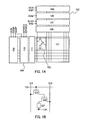
- FIG. 1A A configuration of an active matrix display device of the invention is described with reference to FIG. 1A .
- a pixel portion 101 a plurality of pixels 102 each surrounded by a dotted line frame are arranged in matrix.
- a source driver 103 and a gate driver 104 are provided at the periphery of the pixel portion 101.
- the source driver 103 has a shift register 105, a first latch circuit 106, a second latch circuit 107, and level shifter and buffer 108.
- the gate driver 104 has a shift register 109, an RS latch 110, and level shifter and buffer 111.
- Each pixel 102 has a source signal line 121 connected to the source driver 103, a gate signal line 122 connected to the gate driver 104, a current supply line 123, an opposite electrode 124, a switching TFT 125 connected to the source signal line 121 and the gate signal line 122, a driving TFT 126 connected to the current supply line 123, and a light emitting element 127 connected to the driving TFT 126 and the opposite electrode 124.
- the pixel 102 is driven in different manners depending on the conductivity of the TFTs constituting the pixel, the direction of current flowing through the light emitting element, and the like.
- This embodiment mode shows an example where an N-channel TFT is used as the switching TFT 125, a P-channel TFT is used as the driving TFT 126, and current flows through the light emitting element 127 from the current supply line 123 with a higher potential to the opposite electrode 124 with a lower potential.
- the logic of all circuits is described taking as an example the case where the pixel shown here is driven. However, it is needless to say that if the logic of signals and the relationship between power supplies are changed, the invention can also be applied to the case where a pixel having another configuration is driven.
- the conductivity and the like of the TFTs are not particularly limited.
- the gate signal line 122 In a row that is not selected, the gate signal line 122 is at Low level and the switching TFT 125 is turned off. Meanwhile, in a row where pixels are selected, the gate signal line 122 is at High level and the switching TFT 125 is turned on, so that the potential of the source signal line 121 is written to a gate electrode of the driving TFT 126.
- the driving TFT 126 is turned off and no current flows through the light emitting element 127; therefore, the pixel displays black.
- the driving TFT 126 is turned on and current flows through the light emitting element 127; therefore, the pixel displays white.
- a video signal written to the gate electrode of the driving TFT 126 is preferably held in a storage capacitor or the like during a certain period. According to this, after the gate signal line 122 is changed into a non-selective state, the on state or the off state of the driving TFT 126, namely a black display or a white display can be maintained.
- the shift register 105 sequentially outputs sampling pulses from the first stage in accordance with a clock signal (SCK) and a start pulse (SSP).
- a video signal (Data) is sampled by the first latch circuit 106 in accordance with the sampling pulses outputted from the shift register 105.
- the inputted video signal is held in a memory portion of the first latch circuit 106 until the sampling is completed in the last stage.
- one-row data held in the first latch circuit 106 is simultaneously transferred to the second latch circuit 107 in accordance with a latch pulse (SLAT).
- a writing/erasing selection signal (hereinafter referred to as W/E signal) selects a mode of charging/discharging the source signal lines in accordance with the video signals, and a mode of outputting an erasing signal to all the source signal lines.
- the shift register 109 sequentially outputs row selection pulses from the first stage in accordance with a clock signal (GCK), and a start pulse 1 (G1SP) or a start pulse 2 (G2SP).
- a pulse width control signal 1 (GPWC1) having a half period of the clock signal (GCK) and a pulse width control signal 2 (GPWC2) that is an inverted signal of the pulse width control signal 1 (GPWC1) are inputted to the gate driver 104.
- the RS latch 110 As for the first stage of the RS latch 110, when the start pulse 1 (G1SP) is inputted to the shift register 109, the output of the RS latch does not change and an initial state is held. As the initial state is held, the RS latch selects the pulse width control signal 1 (GPWC1), and the logical AND between the pulse width control signal 1 (GPWC1) and the row selection pulse of the shift register 109 of the row is inputted to the level shifter and buffer 111 of the row. As a result, the level shifter and buffer 111 of the row outputs a writing signal to the gate signal line.
- GPWC1 pulse width control signal 1
- the logical AND between the pulse width control signal 1 (GPWC1) and the row selection pulse of the shift register 109 is inputted to the level shifter and buffer 111 of the row.
- the level shifter and buffer 111 of the row outputs a writing signal to the gate signal line.
- FIG. 6A Such a series of operations is briefly shown in FIG. 6A .
- GSR1, GSR2, and GSR3 are outputs of the shift register 109, and GLine1, GLine2, and GLine3 are gate signal lines and signals inputted thereto are shown.
- the start pulse 2 (G2SP) is inputted to the shift register 109
- the output of the first stage of the RS latch 110 is inverted (set) to the initial state.
- the RS latch 110 selects the pulse width control signal 2 (GPWC2), and the logical AND between the pulse width control signal 2 (GPWC2) and the row selection pulse of the shift register 109 of the row is inputted to the level shifter and buffer 111 of the row. As a result, an erasing signal is outputted to the gate signal line.
- the output of second stage or later of the RS latch 110 in accordance with the output that is inverted (set) to the initial state of the RS latch of the several stages before, the logical AND between the pulse width control signal 2 (GPWC2) and the row selection pulse of the shift register 109 is inputted to the level shifter and buffer 111 of the row, and an erasing signal is outputted to the gate signal line.
- the output of the previous RS latches is inputted to each RS latch.
- the output of the RS latch is reset and returned to the initial state.
- FIG. 6B Such a series of operations is briefly shown in FIG. 6B .
- GSR1, GSR2, and GSR3 are outputs of the shift register 109, and GLine1, GLine2, and GLine3 are gate signal lines and signals inputted thereto are shown.
- the input of the start pulse 2 (G2SP) is delayed by an integer (integer of 2 or more) multiple of the clock signal (GCK) period from the input of the start pulse 1 (G1SP).
- the writing operation and the erasing operation can be performed in one horizontal period. That is to say, the gate driver 104 of the invention can be considered to be one gate driver that has two functions of the writing gate driver and the erasing gate driver.
- the gate driver 104 of the invention is provided on only one side of the pixel portion 101, a smaller bezel can be achieved as compared to the case where the writing gate driver and the erasing gate driver are provided on opposite sides.
- the gate driver 104 of the invention is provided on only one side of the pixel portion 101, the number of shift registers 109 is reduced to half that in the case where the writing gate driver and the erasing gate driver are provided on opposite sides of the pixel portion. Thus, power consumption can be reduced.
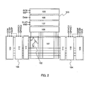
- the gate drivers 104 each having the shift register 109, the RS latch 110, and the level shifter and buffer 111 are provided on opposite sides of the pixel portion 101 and the same signal is outputted from the opposite sides to the same gate signal line at a time, the signal can be transmitted to the gate signal line faster. As a result, a display device with high definition can be achieved even when a horizontal period is reduced and the load of a gate line is increased.
- FIG. 2 the identical portions to those in FIG. 1A are denoted by the identical reference numerals.
- the gate driver in this embodiment mode has the same configuration as that shown in FIG. 1A .
- This embodiment mode is different from Embodiment Mode 1 in that the gate drivers 104 are provided on opposite sides of the pixel portion 101.
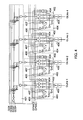
- Described in this embodiment mode is a configuration example of a driver circuit of the display device of the invention, namely a source driver and a gate driver.
- the source driver has a shift register 301, a first latch circuit 302, a second latch circuit 303, a writing/erasing selection circuit 304, and a buffer circuit 305.
- the shift register 301 sequentially outputs sampling pulses in accordance with clock signals (SCK, SCKb: inverted signal of SCK) and a start pulse (SSP).
- a video signal (Data) is sampled by the first latch circuit 302 in accordance with the sampling pulses outputted from the shift register 301.
- latch pulses SLAT, SLATb: inverted signal of SLAT
- the writing/erasing selection circuit 304 outputs an inverted signal of the video signal if a W/E signal is active (herein at High level).
- the writing/erasing selection circuit 304 outputs a High level signal regardless of the video signal. Then, source signal lines (SLine 1 to SLine n) (n is an integer of 2 or more) are charged/discharged through the buffer circuit 305.
- the gate driver has a shift register 401, a selector circuit 402, an RS latch circuit 403, an inverter circuit 406, an inverter circuit 407, an AND circuit 404, and a buffer circuit 405.
- An input of the inverter circuit 406 is connected to an output of the AND circuit 404 of two stages before, and an input of the inverter circuit 407 is connected to an output of the AND circuit 404 of two stages later.
- the input of the inverter circuit 406 is a set input of the RS latch circuit 403, and the input of the inverter circuit 407 is a reset input of the RS latch circuit 403.
- a start pulse 2 is connected to the inputs of the inverter circuits 406 of the first and second stages.
- a start pulse 1 G1SP
- the logical AND between a pulse width control signal 1 GPWC1
- a row selection pulse of the shift register 401 is outputted to gate lines (GLine1, GLine2, GLine3, and GLine4).
- GPWC1 pulse width control signal 1
- GPWC2 pulse width control signal 2
- GPWC2 pulse width control signal 2
- the row selection pulse of the shift register 401 is outputted to the gate lines (GLine1, GLine2, GLine3, and GLine4).
- the selector circuit 402, the RS latch circuit 403, the inverter circuit 405, the inverter circuit 407, and the AND circuit 404 can be collectively referred to as a control circuit.
- level shifter is not provided in the gate driver and the source driver of this embodiment mode, it may be provided as needed.
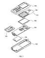
- FIG. 7 shows an example of a mobile phone that incorporates a display device using the gate driver and the source driver described in this specification, for example an electroluminescence (EL) display device.
- EL electroluminescence
- the configuration of the pixel of the electroluminescence (EL) display device is not limited to that described in Embodiment Mode 1 with reference to FIG. 1B .
- one or both of the switching TFT and the driving TFT may adopt a so-called multi-gate structure where a plurality of TFTs are serially connected.
- the two kinds of TFTs of the switching TFT and the driving TFT are not necessarily employed.
- the cross sectional structure and the conductivity (N-channel or P-channel) of each TFT are not particularly limited.
- Layers constituting a light emitting element, insulating films, electrodes, and wires may be formed using any known material and method.
- a display device 701 is incorporated in a housing 702 so as to be detachable.
- the shape and size of the housing 702 may be appropriately changed in accordance with the size of the display device 701.
- the housing incorporating the display device 701 is mounted onto a printed wiring board 703 to complete a module.
- the display device 701 is connected to the printed wiring board 703 through an FPC 708.
- the printed wiring board 703 has a speaker, a microphone, a transmitting/receiving circuit, and a signal processing circuit including a CPU, a controller and the like.
- Such a module is combined with an input means 704 and a battery 705, and put in housings 700 and 706.
- a pixel portion of the display device 701 is disposed to be seen from a window formed in the housing 700.
- the mobile phone described in this embodiment can be used in various modes depending on the function and application thereof. The same effect can be achieved even when, for example, a plurality of display devices are provided, or the housing is divided into two or more parts so as to be opened and closed with a hinge.
- FIG. 8A shows a display device having a display panel 801 and a circuit board 802, which is incorporated in a television receiver.
- the display device is, for example, an electroluminescence (EL) display device that uses the source driver and the gate driver described in this specification.
- EL electroluminescence
- the configuration of the pixel of the electroluminescence (EL) display device is not limited to that described in Embodiment Mode 1 with reference to FIG. 1B .
- one or both of the switching TFT and the driving TFT may adopt a so-called multi-gate structure where a plurality of TFTs are serially connected.
- the two kinds of TFTs of the switching TFT and the driving TFT are not necessarily employed.
- the cross sectional structure and the conductivity (N-channel or P-channel) of each TFT are not particularly limited.
- Layers constituting a light emitting element, insulating films, electrodes, and wires may be formed using any known material and method.
- the circuit board 802 has, for example, a control circuit 803, a signal dividing circuit 804 and the like. Although a source driver 805 and a gate driver 806 are formed over the same substrate as a pixel portion 807 in FIG. 8A , only the gate driver 806 may be formed over the same substrate as the pixel portion 807. As described in Embodiment Mode 1, the gate driver 806 may be provided on only one side of the pixel portion 807.
- FIG. 8A When the display device shown in FIG. 8A is incorporated in a housing 811, a television receiver as shown in FIG. 8B can be completed.
- Reference numeral 812 denotes a display screen, and speakers 813 and an operating switch 814 are appropriately provided.
- the invention By applying the invention to the display device incorporated in the television receiver, reduced power consumption as well as a smaller bezel can be achieved.
- the smaller bezel allows the display screen 812 to occupy a larger area.
- FIGS. 9A and 9B show an example of a digital camera that incorporates a display device using the gate driver and the source driver described in this specification, for example, an electroluminescence (EL) display device.
- EL electroluminescence
- the configuration of the pixel of the electroluminescence (EL) display device is not limited to that described in Embodiment Mode 1 with reference to FIG. 1B .
- one or both of the switching TFT and the driving TFT may adopt a so-called multi-gate structure where a plurality of TFTs are serially connected.
- the two kinds of TFTs of the switching TFT and the driving TFT are not necessarily employed.
- the cross sectional structure and the conductivity (N-channel or P-channel) of each TFT are not particularly limited.
- Layers constituting a light emitting element, insulating films, electrodes, and wires may be formed using any known material and method.
- FIG. 9A is a front view of a digital camera.
- Reference numeral 901 denotes a release button
- 902 denotes a main switch
- 903 denotes a finder
- 904 denotes an electronic flash
- 905 denotes a lens
- 906 denotes a housing.
- FIG. 9B is a back view of the digital camera shown in FIG. 9A .
- Reference numeral 907 denotes a finder eyepiece
- 908 denotes a monitor
- 909 and 910 denote operating buttons.
- the application of the invention is not limited to the mobile phone described in Embodiment 1, the television receiver described in Embodiment 2, and the digital camera described in Embodiment 3, and the invention can be applied to all electronic apparatuses incorporating the display device.
Landscapes
- Engineering & Computer Science (AREA)
- Physics & Mathematics (AREA)
- Computer Hardware Design (AREA)
- General Physics & Mathematics (AREA)
- Theoretical Computer Science (AREA)
- Chemical & Material Sciences (AREA)
- Crystallography & Structural Chemistry (AREA)
- Control Of Indicators Other Than Cathode Ray Tubes (AREA)
Claims (3)
- Anzeigevorrichtung, die umfasst:Gate-Signalleitungen (122), die in einer Vielzahl von Zeilen angeordnet sind;Source-Signalleitungen (121), die in einer Vielzahl von Spalten angeordnet sind;einen Pixelabschnitt (101), der eine Vielzahl von Pixeln (102) aufweist, wobei jedes Pixel des Pixelabschnitts von benachbarten Leitungen der Gate-Signalleitungen (122) und benachbarten Leitungen der Source-Signalleitungen (121) umgeben ist;eine Source-Signalleitungs-Treiberschaltung (103), die elektrisch mit den Source-Signalleitungen (121) verbunden ist; undeine Gate-Signalleitungs-Treiberschaltung (104), die elektrisch mit den Gate-Signalleitungen (122) verbunden ist, wobei die Gate-Signalleitungs-Treiberschaltung (104) aufweist: ein Schieberegister (401) zum Auswählen der Zeilen und eine Steuerschaltung zum Schalten zwischen einer Schreiboperation eines Bildsignals in die Vielzahl von Pixeln und einer Löschoperation des geschriebenen Bildsignals in der Vielzahl von Pixeln während der gleichen horizontalen Abtastperiode, wobei die Steuerschaltung eine Vielzahl von Nebenschaltungen umfasst,wobei jede der Nebenschaltungen ferner dadurch gekennzeichnet ist, dass sie umfasst:eine erste Inverterschaltung (406);eine zweite Inverterschaltung (407);eine AND-Schaltung (404);eine Rücksetz-Setz-Latch-Schaltung (403); undeine Auswahlschaltung (402), die angeordnet ist, um ein erstes Impulsbreite-Steuersignal (GPWC1) und ein zweites Impulsbreite-Steuersignal (GPWC2) zu empfangen und um durch eine Ausgabe der Rücksetz-Setz-Latch-Schaltung (403) gesteuert zu werden, wobei eine Eingabe der ersten Inverterschaltung (406) eine Setz-Eingabe der Rücksetz-Setz-Latch-Schaltung (403) ist und eine Eingabe der zweiten Inverterschaltung (407) eine Rücksetz-Eingabe der Rücksetz-Setz-Latch-Schaltung (403) ist;wobei Eingänge der Auswahlschaltungen (402) mit dem Schieberegister (401) verbunden sind;wobei das Schieberegister (401) und die Steuerschaltung konfiguriert sind, um ein Signal (G2SP) zum Beginnen der Löschoperation zu empfangen; undwobei der Eingang der ersten Inverterschaltung (406) einer der Nebenschaltungen mit einem Ausgang einer AND-Schaltung (404) einer Nebenschaltung, die sich zwei Nebenschaltungen vor der einen der Nebenschaltungen befindet, verbunden ist, und der Eingang der zweiten Inverterschaltung (407) der einen der Nebenschaltungen mit einem Ausgang einer AND-Schaltung (404) einer Nebenschaltung, die sich zwei Nebenschaltungen nach der einen der Nebenschaltungen befindet, verbunden ist.
- Anzeigevorrichtung nach Anspruch 1, wobei die Gate-Signalleitungs-Treiberschaltung (104) auf gegenüberliegenden Seiten des Pixelabschnitts (101) vorgesehen ist.
- Anzeigevorrichtung nach Anspruch 1, wobei die Anzeigevorrichtung für ein elektronisches Gerät verwendet wird, das aus einer Gruppe ausgewählt wird, die aus einem Mobiltelefon, einer Digitalkamera und einem Fernsehempfänger besteht.
Applications Claiming Priority (2)
| Application Number | Priority Date | Filing Date | Title |
|---|---|---|---|
| JP2004353445 | 2004-12-06 | ||
| PCT/JP2005/022707 WO2006062212A1 (en) | 2004-12-06 | 2005-12-05 | Display device and electronic apparatus using the same |
Publications (3)
| Publication Number | Publication Date |
|---|---|
| EP1820180A1 EP1820180A1 (de) | 2007-08-22 |
| EP1820180A4 EP1820180A4 (de) | 2010-02-03 |
| EP1820180B1 true EP1820180B1 (de) | 2014-10-15 |
Family
ID=36578029
Family Applications (1)
| Application Number | Title | Priority Date | Filing Date |
|---|---|---|---|
| EP05814448.6A Expired - Lifetime EP1820180B1 (de) | 2004-12-06 | 2005-12-05 | Anzeigeeinrichtung und elektronische vorrichtung damit |
Country Status (4)
| Country | Link |
|---|---|
| US (1) | US8570266B2 (de) |
| EP (1) | EP1820180B1 (de) |
| KR (1) | KR101280293B1 (de) |
| WO (1) | WO2006062212A1 (de) |
Families Citing this family (7)
| Publication number | Priority date | Publication date | Assignee | Title |
|---|---|---|---|---|
| KR20070052051A (ko) * | 2005-11-16 | 2007-05-21 | 삼성전자주식회사 | 액정 표시 장치의 구동 장치 및 이를 포함하는 액정 표시장치 |
| US8031179B2 (en) * | 2006-06-30 | 2011-10-04 | Canon Kabushiki Kaisha | Control apparatus for operation panel and electronic apparatus |
| US20100324091A1 (en) | 2007-06-27 | 2010-12-23 | Kowa Company, Ltd. | Pyrazolone Derivative |
| JP5839896B2 (ja) * | 2010-09-09 | 2016-01-06 | 株式会社半導体エネルギー研究所 | 表示装置 |
| US10102792B2 (en) * | 2016-03-30 | 2018-10-16 | Novatek Microelectronics Corp. | Driving circuit of display panel and display apparatus using the same |
| CN108831392A (zh) * | 2018-06-25 | 2018-11-16 | 武汉天马微电子有限公司 | 显示面板和显示装置 |
| KR102870521B1 (ko) * | 2020-08-04 | 2025-10-16 | 삼성디스플레이 주식회사 | 표시장치 |
Family Cites Families (30)
| Publication number | Priority date | Publication date | Assignee | Title |
|---|---|---|---|---|
| US5790089A (en) | 1991-03-20 | 1998-08-04 | Seiko Epson Corporation | Method of driving an active matrix type liquid crystal display |
| JP3211256B2 (ja) | 1991-04-09 | 2001-09-25 | 松下電器産業株式会社 | 液晶表示装置とそれを用いた液晶投写型テレビ |
| JP4092857B2 (ja) * | 1999-06-17 | 2008-05-28 | ソニー株式会社 | 画像表示装置 |
| JP2001166280A (ja) | 1999-12-10 | 2001-06-22 | Nec Corp | 液晶表示装置の駆動方法 |
| US7129918B2 (en) | 2000-03-10 | 2006-10-31 | Semiconductor Energy Laboratory Co., Ltd. | Electronic device and method of driving electronic device |
| JP2001324958A (ja) | 2000-03-10 | 2001-11-22 | Semiconductor Energy Lab Co Ltd | 電子装置およびその駆動方法 |
| JP4776829B2 (ja) | 2000-09-08 | 2011-09-21 | 株式会社半導体エネルギー研究所 | 自発光装置 |
| US7053874B2 (en) | 2000-09-08 | 2006-05-30 | Semiconductor Energy Laboratory Co., Ltd. | Light emitting device and driving method thereof |
| JP3812340B2 (ja) | 2001-01-15 | 2006-08-23 | 株式会社日立製作所 | 画像表示装置 |
| JP3862966B2 (ja) | 2001-03-30 | 2006-12-27 | 株式会社日立製作所 | 画像表示装置 |
| JP3959256B2 (ja) * | 2001-11-02 | 2007-08-15 | 東芝松下ディスプレイテクノロジー株式会社 | アクティブマトリックス表示パネルの駆動装置 |
| JP3800404B2 (ja) | 2001-12-19 | 2006-07-26 | 株式会社日立製作所 | 画像表示装置 |
| JP4350334B2 (ja) | 2002-01-25 | 2009-10-21 | シャープ株式会社 | 表示素子の点灯制御方法および表示制御方法、ならびに表示装置 |
| JP2003255912A (ja) | 2002-03-05 | 2003-09-10 | Seiko Epson Corp | 電気光学装置、それを用いた電子機器および電気光学装置の駆動方法 |
| JP2003321081A (ja) | 2002-04-30 | 2003-11-11 | Ricoh Co Ltd | 情報記録媒体の包装構造 |
| JP2003347237A (ja) | 2002-05-30 | 2003-12-05 | Mitsubishi Electric Corp | 半導体装置の製造方法およびその製造装置 |
| JP3901048B2 (ja) | 2002-07-24 | 2007-04-04 | 日本ビクター株式会社 | アクティブマトリクス型液晶表示装置 |
| JP2004063924A (ja) | 2002-07-31 | 2004-02-26 | Mitsubishi Heavy Ind Ltd | レーザアニール方法及び装置 |
| JP4701589B2 (ja) | 2002-09-30 | 2011-06-15 | セイコーエプソン株式会社 | 液晶装置と投射型表示装置 |
| GB2397710A (en) | 2003-01-25 | 2004-07-28 | Sharp Kk | A shift register for an LCD driver, comprising reset-dominant RS flip-flops |
| US7327916B2 (en) | 2003-03-11 | 2008-02-05 | Semiconductor Energy Laboratory Co., Ltd. | Beam Homogenizer, laser irradiation apparatus, and method of manufacturing a semiconductor device |
| JP4390469B2 (ja) | 2003-03-26 | 2009-12-24 | Necエレクトロニクス株式会社 | 画像表示装置、該画像表示装置に用いられる信号線駆動回路及び駆動方法 |
| JP2004294672A (ja) | 2003-03-26 | 2004-10-21 | Seiko Epson Corp | 電気光学装置及びその駆動方法並びに電子機器 |
| JP3821111B2 (ja) | 2003-05-12 | 2006-09-13 | セイコーエプソン株式会社 | データドライバ及び電気光学装置 |
| JP4413528B2 (ja) | 2003-05-16 | 2010-02-10 | 株式会社半導体エネルギー研究所 | レーザ照射装置 |
| JP2004342954A (ja) | 2003-05-19 | 2004-12-02 | Ishikawajima Harima Heavy Ind Co Ltd | レーザアニール方法及び装置 |
| JP4171399B2 (ja) | 2003-10-30 | 2008-10-22 | 住友重機械工業株式会社 | レーザ照射装置 |
| JP2005173418A (ja) * | 2003-12-15 | 2005-06-30 | Tohoku Pioneer Corp | 発光表示パネルの駆動装置 |
| US7215306B2 (en) * | 2003-12-22 | 2007-05-08 | Wintek Corporation | Driving apparatus for an active matrix organic light emitting display |
| JP2005217209A (ja) | 2004-01-30 | 2005-08-11 | Hitachi Ltd | レーザアニール方法およびレーザアニール装置 |
-
2005
- 2005-12-05 US US11/719,785 patent/US8570266B2/en not_active Expired - Fee Related
- 2005-12-05 KR KR1020077013920A patent/KR101280293B1/ko not_active Expired - Fee Related
- 2005-12-05 EP EP05814448.6A patent/EP1820180B1/de not_active Expired - Lifetime
- 2005-12-05 WO PCT/JP2005/022707 patent/WO2006062212A1/en not_active Ceased
Also Published As
| Publication number | Publication date |
|---|---|
| US8570266B2 (en) | 2013-10-29 |
| EP1820180A4 (de) | 2010-02-03 |
| KR20070091147A (ko) | 2007-09-07 |
| KR101280293B1 (ko) | 2013-07-01 |
| US20090146920A1 (en) | 2009-06-11 |
| WO2006062212A1 (en) | 2006-06-15 |
| EP1820180A1 (de) | 2007-08-22 |
Similar Documents
| Publication | Publication Date | Title |
|---|---|---|
| JP4494214B2 (ja) | 表示装置、電子機器 | |
| US8310433B2 (en) | Display device and electronic apparatus | |
| KR100924740B1 (ko) | 신호선 구동회로 및 발광장치 | |
| US6867761B2 (en) | Electro-optical device and method of driving the same, organic electroluminescent display device, and electronic apparatus | |
| KR100506355B1 (ko) | 전기 광학 장치, 전기 광학 장치의 구동 방법, 전기 광학장치의 주사선 선택 방법 및 전자 기기 | |
| JP4244617B2 (ja) | 電気光学装置、電気光学装置の駆動方法 | |
| US20120200612A1 (en) | Driving Method of Display Device | |
| JP2006003752A (ja) | 表示装置及びその駆動制御方法 | |
| KR100857517B1 (ko) | 유기 el 장치, 회로, 유기 el 장치의 구동 방법 및 전자 기기 | |
| US20070229413A1 (en) | Electro-optical device, method for driving electro-optical device, and electronic apparatus | |
| US7652645B2 (en) | Light emitting display | |
| JP5137294B2 (ja) | 発光装置の駆動方法 | |
| EP1820180B1 (de) | Anzeigeeinrichtung und elektronische vorrichtung damit | |
| JP4743485B2 (ja) | 表示装置及びその表示駆動方法 | |
| US7864139B2 (en) | Organic EL device, driving method thereof, and electronic apparatus | |
| JP2008170842A (ja) | 電気光学装置、駆動回路および電子機器 | |
| JP4604455B2 (ja) | 電気光学装置、電気光学装置の駆動方法及び電子機器 | |
| JP5008302B2 (ja) | 表示装置 | |
| JP5235048B2 (ja) | 表示装置、電子機器 | |
| JP2006011251A (ja) | 電気光学装置、その駆動方法および電子機器 | |
| JP2004317576A (ja) | 駆動回路、駆動方法、電気光学装置、及び電子機器 | |
| US20100259571A1 (en) | Electro-optical apparatus, driving method thereof and electronic device | |
| JP2004004638A (ja) | 発光装置の駆動方法 |
Legal Events
| Date | Code | Title | Description |
|---|---|---|---|
| PUAI | Public reference made under article 153(3) epc to a published international application that has entered the european phase |
Free format text: ORIGINAL CODE: 0009012 |
|
| 17P | Request for examination filed |
Effective date: 20070521 |
|
| AK | Designated contracting states |
Kind code of ref document: A1 Designated state(s): DE FI FR GB NL |
|
| DAX | Request for extension of the european patent (deleted) | ||
| RBV | Designated contracting states (corrected) |
Designated state(s): DE FI FR GB NL |
|
| A4 | Supplementary search report drawn up and despatched |
Effective date: 20100108 |
|
| RIC1 | Information provided on ipc code assigned before grant |
Ipc: G09G 3/30 20060101AFI20060621BHEP Ipc: G09G 3/20 20060101ALI20091230BHEP Ipc: G09G 3/36 20060101ALI20091230BHEP Ipc: G11C 19/28 20060101ALI20091230BHEP |
|
| 17Q | First examination report despatched |
Effective date: 20100510 |
|
| GRAP | Despatch of communication of intention to grant a patent |
Free format text: ORIGINAL CODE: EPIDOSNIGR1 |
|
| INTG | Intention to grant announced |
Effective date: 20140616 |
|
| GRAS | Grant fee paid |
Free format text: ORIGINAL CODE: EPIDOSNIGR3 |
|
| GRAA | (expected) grant |
Free format text: ORIGINAL CODE: 0009210 |
|
| AK | Designated contracting states |
Kind code of ref document: B1 Designated state(s): DE FI FR GB NL |
|
| REG | Reference to a national code |
Ref country code: GB Ref legal event code: FG4D |
|
| REG | Reference to a national code |
Ref country code: DE Ref legal event code: R096 Ref document number: 602005044953 Country of ref document: DE Effective date: 20141127 |
|
| REG | Reference to a national code |
Ref country code: NL Ref legal event code: VDEP Effective date: 20141015 |
|
| PG25 | Lapsed in a contracting state [announced via postgrant information from national office to epo] |
Ref country code: NL Free format text: LAPSE BECAUSE OF FAILURE TO SUBMIT A TRANSLATION OF THE DESCRIPTION OR TO PAY THE FEE WITHIN THE PRESCRIBED TIME-LIMIT Effective date: 20141015 |
|
| PG25 | Lapsed in a contracting state [announced via postgrant information from national office to epo] |
Ref country code: FI Free format text: LAPSE BECAUSE OF FAILURE TO SUBMIT A TRANSLATION OF THE DESCRIPTION OR TO PAY THE FEE WITHIN THE PRESCRIBED TIME-LIMIT Effective date: 20141015 |
|
| REG | Reference to a national code |
Ref country code: DE Ref legal event code: R097 Ref document number: 602005044953 Country of ref document: DE |
|
| PLBE | No opposition filed within time limit |
Free format text: ORIGINAL CODE: 0009261 |
|
| STAA | Information on the status of an ep patent application or granted ep patent |
Free format text: STATUS: NO OPPOSITION FILED WITHIN TIME LIMIT |
|
| 26N | No opposition filed |
Effective date: 20150716 |
|
| GBPC | Gb: european patent ceased through non-payment of renewal fee |
Effective date: 20150115 |
|
| REG | Reference to a national code |
Ref country code: FR Ref legal event code: ST Effective date: 20150831 |
|
| PG25 | Lapsed in a contracting state [announced via postgrant information from national office to epo] |
Ref country code: GB Free format text: LAPSE BECAUSE OF NON-PAYMENT OF DUE FEES Effective date: 20150115 |
|
| PG25 | Lapsed in a contracting state [announced via postgrant information from national office to epo] |
Ref country code: FR Free format text: LAPSE BECAUSE OF NON-PAYMENT OF DUE FEES Effective date: 20141231 |
|
| PGFP | Annual fee paid to national office [announced via postgrant information from national office to epo] |
Ref country code: DE Payment date: 20201124 Year of fee payment: 16 |
|
| REG | Reference to a national code |
Ref country code: DE Ref legal event code: R119 Ref document number: 602005044953 Country of ref document: DE |
|
| PG25 | Lapsed in a contracting state [announced via postgrant information from national office to epo] |
Ref country code: DE Free format text: LAPSE BECAUSE OF NON-PAYMENT OF DUE FEES Effective date: 20220701 |