EP1811559A1 - Substrate supporting/transferring tray - Google Patents
Substrate supporting/transferring tray Download PDFInfo
- Publication number
- EP1811559A1 EP1811559A1 EP05795512A EP05795512A EP1811559A1 EP 1811559 A1 EP1811559 A1 EP 1811559A1 EP 05795512 A EP05795512 A EP 05795512A EP 05795512 A EP05795512 A EP 05795512A EP 1811559 A1 EP1811559 A1 EP 1811559A1
- Authority
- EP
- European Patent Office
- Prior art keywords
- substrate
- substrate supporting
- transferring tray
- tray
- transferring
- Prior art date
- Legal status (The legal status is an assumption and is not a legal conclusion. Google has not performed a legal analysis and makes no representation as to the accuracy of the status listed.)
- Withdrawn
Links
Images



Classifications
-
- H—ELECTRICITY
- H10—SEMICONDUCTOR DEVICES; ELECTRIC SOLID-STATE DEVICES NOT OTHERWISE PROVIDED FOR
- H10P—GENERIC PROCESSES OR APPARATUS FOR THE MANUFACTURE OR TREATMENT OF DEVICES COVERED BY CLASS H10
- H10P72/00—Handling or holding of wafers, substrates or devices during manufacture or treatment thereof
- H10P72/70—Handling or holding of wafers, substrates or devices during manufacture or treatment thereof for supporting or gripping
-
- H—ELECTRICITY
- H10—SEMICONDUCTOR DEVICES; ELECTRIC SOLID-STATE DEVICES NOT OTHERWISE PROVIDED FOR
- H10P—GENERIC PROCESSES OR APPARATUS FOR THE MANUFACTURE OR TREATMENT OF DEVICES COVERED BY CLASS H10
- H10P72/00—Handling or holding of wafers, substrates or devices during manufacture or treatment thereof
- H10P72/04—Apparatus for manufacture or treatment
- H10P72/0431—Apparatus for thermal treatment
- H10P72/0432—Apparatus for thermal treatment mainly by conduction
-
- H—ELECTRICITY
- H10—SEMICONDUCTOR DEVICES; ELECTRIC SOLID-STATE DEVICES NOT OTHERWISE PROVIDED FOR
- H10P—GENERIC PROCESSES OR APPARATUS FOR THE MANUFACTURE OR TREATMENT OF DEVICES COVERED BY CLASS H10
- H10P72/00—Handling or holding of wafers, substrates or devices during manufacture or treatment thereof
- H10P72/10—Handling or holding of wafers, substrates or devices during manufacture or treatment thereof using carriers specially adapted therefor, e.g. front opening unified pods [FOUP]
- H10P72/18—Handling or holding of wafers, substrates or devices during manufacture or treatment thereof using carriers specially adapted therefor, e.g. front opening unified pods [FOUP] characterised by being specially adapted for supporting a single substrate or by comprising a stack of such individual supports
-
- H—ELECTRICITY
- H10—SEMICONDUCTOR DEVICES; ELECTRIC SOLID-STATE DEVICES NOT OTHERWISE PROVIDED FOR
- H10P—GENERIC PROCESSES OR APPARATUS FOR THE MANUFACTURE OR TREATMENT OF DEVICES COVERED BY CLASS H10
- H10P72/00—Handling or holding of wafers, substrates or devices during manufacture or treatment thereof
- H10P72/70—Handling or holding of wafers, substrates or devices during manufacture or treatment thereof for supporting or gripping
- H10P72/72—Handling or holding of wafers, substrates or devices during manufacture or treatment thereof for supporting or gripping using electrostatic chucks
-
- H—ELECTRICITY
- H10—SEMICONDUCTOR DEVICES; ELECTRIC SOLID-STATE DEVICES NOT OTHERWISE PROVIDED FOR
- H10P—GENERIC PROCESSES OR APPARATUS FOR THE MANUFACTURE OR TREATMENT OF DEVICES COVERED BY CLASS H10
- H10P72/00—Handling or holding of wafers, substrates or devices during manufacture or treatment thereof
- H10P72/70—Handling or holding of wafers, substrates or devices during manufacture or treatment thereof for supporting or gripping
- H10P72/76—Handling or holding of wafers, substrates or devices during manufacture or treatment thereof for supporting or gripping using mechanical means, e.g. clamps or pinches
- H10P72/7604—Handling or holding of wafers, substrates or devices during manufacture or treatment thereof for supporting or gripping using mechanical means, e.g. clamps or pinches the wafers being placed on a susceptor, stage or support
-
- H—ELECTRICITY
- H10—SEMICONDUCTOR DEVICES; ELECTRIC SOLID-STATE DEVICES NOT OTHERWISE PROVIDED FOR
- H10P—GENERIC PROCESSES OR APPARATUS FOR THE MANUFACTURE OR TREATMENT OF DEVICES COVERED BY CLASS H10
- H10P72/00—Handling or holding of wafers, substrates or devices during manufacture or treatment thereof
- H10P72/70—Handling or holding of wafers, substrates or devices during manufacture or treatment thereof for supporting or gripping
- H10P72/76—Handling or holding of wafers, substrates or devices during manufacture or treatment thereof for supporting or gripping using mechanical means, e.g. clamps or pinches
- H10P72/7604—Handling or holding of wafers, substrates or devices during manufacture or treatment thereof for supporting or gripping using mechanical means, e.g. clamps or pinches the wafers being placed on a susceptor, stage or support
- H10P72/7611—Handling or holding of wafers, substrates or devices during manufacture or treatment thereof for supporting or gripping using mechanical means, e.g. clamps or pinches the wafers being placed on a susceptor, stage or support characterised by edge profile or support profile
Definitions
- the present invention relates to a substrate supporting/transferring tray that is provided so that it can be placed on a substrate supporting member arranged in a treatment chamber where the heat treatment occurs for a semiconductor substrate that is placed on the upper side of the substrate supporting member. More specifically, the present invention also relates to a substrate supporting/transferring tray that can be placed on a substrate supporting member incorporating a heating means therein for heating the substrate that is placed on the upper side of the substrate supporting member.
- the heat treatment may occur for the semiconductor substrate as it is placed on the substrate supporting/transferring tray having a substrate supporting part on its upper side, in order to ensure that the semiconductor substrate can be heated uniformly during the heating process or can be transferred to any subsequent process after the heat treatment is completed.
- a semiconductor substrate 1 may be placed on a substrate supporting/transferring tray 18 having a substrate supporting portion on its upper side, and the heat treatment may occur for the substrate 1 under the vacuum condition or atmospheric condition by placing the substrate supporting/transferring tray having the substrate placed thereon onto a substrate supporting member 2 that incorporates a heating means 4 therein for heating the semiconductor substrate.
- the substrate supporting/transferring tray 18 is only intended to heat the substrate 1 uniformly.
- the transfer robot or the like because there is no area on the substrate supporting/transferring tray 18 that can be supported by the transfer robot. The problem is, therefore, that when the heating process is completed for the substrate 1, the substrate 1 cannot be transferred until its temperature is lowered.
- the substrate supporting/transferring tray 18a has the form of a flat plate having a substrate supporting portion on its upper side, and has its outer peripheral edge 18d diametrically larger than the outer peripheral edge 2a of a substrate supporting member 2 incorporating a heating means for heating the substrate. This is disclosed in Japanese patent application as published under H2002 - 2695.
- the transfer robot or the like can be used because the outer peripheral edge 18d is diametrically larger than the outer peripheral edge 2a of the substrate supporting member 2 that incorporates the heating means 4 for heating the substrate, wherein the transfer robot or the like can be operated for causing a pair of forks bifurcated at the forward end thereof to support the underside (bottom side in Fig. 7 (b)) of the outer peripheral edge 18c of the substrate supporting/transferring tray 18a.
- the substrate supporting/transferring tray 18a can be removed from the upper side of the substrate supporting member 2 of the substrate supporting/transferring tray 18a by operating the transfer robot to cause the forward ends of its pair of forks to support the underside (bottom side in Fig. 7 (b)) of the outer peripheral edge 18c of the substrate supporting/transferring tray 18a. This can be accomplished without having to wait for the temperature of the substrate 1 to be lowered. Then, another substrate supporting/transferring tray 18a that follows the preceding substrate supporting/transferring tray and having a new substrate 1 placed on its substrate supporting portion 2 may be transferred onto the substrate supporting member 2 within the treatment chamber where the heating process may occur for the new substrate 1, in the same manner as described above. This permits the heating process to occur efficiently for more than one substrate in sequence.
- One object of the present invention is to provide a substrate supporting/transferring tray having a substrate (semiconductor substrate) placed on its upper side and which may be placed on a substrate supporting member, particularly a substrate supporting member incorporating a heating means therein for heating the substrate that is arranged in the treatment chamber where the heating process occurs for the substrate under the vacuum condition or atmospheric condition, wherein the substrate supporting/transferring tray allows the substrate (semiconductor substrate) to be heated more uniformly during the heating process while at the same time the substrate supporting/transferring tray can easily be removed from the substrate supporting member when the heating process is completed for the substrate, without having to wait until the temperature of the substrate is lowered, and then can be transferred from the treatment chamber into any subsequent process.
- the heating process can occur efficiently for more than one substrate in sequence.
- an embodiment of the substrate supporting/transferring tray proposed by the present invention on the upper side of which a substrate (semiconductor substrate) may be placed, may be placed on the substrate supporting member that is arranged in the treatment chamber in which the heating process occurs for the substrate, wherein the substrate supporting/transferring tray includes a disc-shaped substrate supporting portion located on its upper side, a lateral wall portion that extends downwardly from the peripheral edge of the disc-shaped substrate supporting portion and optimally an annular portion that extends radially outwardly from the bottom end side of the cylindrical lateral wall portion.
- the substrate supporting/transferring tray having a substrate (semiconductor substrate) placed on its upper side and which may be placed on a substrate supporting member, particularly a substrate supporting member incorporating a heating means therein for heating the substrate and which is arranged in the treatment chamber where the heating process occurs for the substrate under the vacuum condition or atmospheric condition, wherein the substrate supporting/transferring tray allows the substrate (semiconductor substrate) to be heated more uniformly during the heating process while at the same time the substrate supporting/transferring tray can easily be removed from the substrate supporting member when the heating process is completed for the substrate, without having to wait until the temperature of the substrate is lowered, and then can be transferred from the treatment chamber into any subsequent process and wherein the heating process can occur efficiently for more than one substrate in sequence.
- a first embodiment of the present invention is described.
- a substrate supporting member 2 is arranged inside a treatment chamber 11 in which heat treatment may be performed for a substrate 1.
- the substrate supporting member 2 has a heater or heating means 4 incorporated therein for heating the substrate, such as a thermoelectron generator intended for heating by electron impact, an infrared lamp intended for heating by infrared rays and the like. In this way, the substrate 1 may be treated thermally inside the treatment chamber 11.
- the treatment chamber 11 in which the heat treatment occurs for the substrate 1 may be placed internally under a specific vacuum condition or under atmospheric condition.
- the substrate supporting/transferring tray 8 may be placed on the substrate supporting member 2, and a substrate (a semiconductor substrate such as Si substrate, SiC substrate and the like, for example) may be placed on the upper side of the substrate supporting member.
- a substrate a semiconductor substrate such as Si substrate, SiC substrate and the like, for example
- the substrate supporting/transferring tray 8 includes a disc-shaped substrate supporting portion 8e (Fig. 3 (a)) on its upper side, and a cylindrical lateral wall portion 9 that extends from the peripheral edge of the disc-shaped substrate supporting portion 8e toward its bottom side.
- the cylindrical lateral wall portion 9 may be formed like a cylindrical shape that extends vertically from the peripheral edge of the disc-shaped substrate supporting portion 8c toward the bottom side (bottom end in Fig. 1) along the outer periphery of the cylindrically-shaped substrate supporting member 2.
- the cylindrical lateral wall portion 9 may be formed like a reversed funnel shape that is becoming diametrically enlarged as it extends vertically from the peripheral edge of the disc-shaped substrate supporting portion 8e toward the bottom side (bottom side in Fig. 1) along the outer periphery of the cylindrically-shaped substrate supporting member 2.
- the cylindrical lateral wall portion 9 should preferably be formed like the cylindrical shape such that it can extend from the peripheral edge of the disc-shaped substrate supporting portion 8e along the outer periphery of the substrate supporting member 8, as shown in Fig. 1.
- An annular portion 10 is provided such that it extends radially outwardly from the bottom side of the cylindrical lateral wall portion 9.
- the substrate supporting/transferring tray 8 in which the substrate 1 is placed on the disc-shaped substrate supporting portion 8e as shown in Fig. 1 may be lifted by operating a transfer robot or the like, which includes a pair of arms 23, 24 at its forward end and a pair of forks 21 a, 21 b bifurcated from its base end 22 linked to the pair of arms 23, 24. Then, the substrate supporting/transferring tray 8 may be transferred by operating the transfer robot to cause its pair of forks 21 a, 21 b to support the bottom side of the annular portion 10.
- the substrate supporting/transferring tray 8 on which that substrate 1 is placed may be removed from the substrate supporting member 2 by operating the transfer robot to cause its pair of forks 21 a, 21 b to support the underside of the annular portion 10 of the substrate supporting/transferring tray 8, without having to wait for the temperature of the substrate 1 to be lowered.
- Another substrate supporting/transferring tray 8 that follows the preceding substrate supporting/transferring tray 8 and having another substrate 1 placed on the disc-shaped substrate supporting portion 8e may be transferred onto the substrate supporting member 2 in the treatment chamber 11 where the heating process may begin for the new substrate 1. In this way, the heating process can occur efficiently for more than one substrate in sequence.
- the substrate supporting/transferring tray 8 includes the cylindrical lateral wall portion 9 extending from the peripheral edge of the disc-shaped substrate supporting portion 8e provided on its upper side toward the bottom side.
- the temperature difference that may occur between the substrate supporting member 2 and substrate supporting/transferring tray 8 when the substrate supporting/transferring tray is heated through the substrate supporting member 2 by the heating means 4 can be kept as small as possible, as compared against the prior art substrate supporting/transferring tray 18, 18a having the form shown in Fig. 7 (a), (b), respectively.
- the temperature distribution inside the surface of the substrate supporting/transferring tray 8 may also be kept as small as possible, as compared against the prior art substrate supporting/transferring tray 18, 18a having the form shown in Fig. 7 (a), (b), respectively.
- the heating can occur more uniformly inside the surface.
- the annular portion 10 is not provided, but only the cylindrical lateral wall portion 9 is provided.
- this embodiment may also provide the effects that are equivalent to those of the embodiments described above.
- the embodiment shown in Fig. 3 represents a variation of the embodiment shown in Fig. 1 in which no annular portion 10 is provided, but only the cylindrical lateral wall portion 9 is provided.
- the embodiment shown in Fig. 4 represents a variation of the embodiment shown in Fig. 2 in which no annular portion 10 is provided, but only the cylindrical lateral wall portion 9 is provided.
- the embodiments shown in Figs. 3 and 4 would be more advantageous if the annular portion 10 is also provided as is the case for the embodiments shown in Figs.
- a cap 5 is mounted on the substrate supporting/transferring tray 8.
- This cap 5 may be provided for covering the substrate 1 (such as SiC substrate) placed on the substrate supporting/transferring tray 8, so that it can cooperate with the substrate supporting/transferring tray 8 to seal the substrate 1 during the heating process.
- the cap 5 may be provided for sealing the space 3 in which the substrate 1 is placed during the heating process. More specifically, the substrate supporting/transferring tray 8 on which the substrate 1 is placed may be covered with the cap 5, thereby sealing the space 3 in which the substrate 1 is placed during the heating process.
- the substrate 1 can be heated more efficiently because the space 3 in which the substrate 1 is placed can be sealed by the cap 5 as described above during the heating process and because of the radiant heat originating from the cap 5.
- the embodiment shown in Fig. 5 (b) differs from the embodiment shown in Fig. 5 (a) in that the cap 5 has a hook step 6 on the bottom side of the lateral wall 5c that is provided for engaging the outer periphery on the upper end of the substrate supporting/transferring tray 8, with the inner diameter R2 of the lateral wall of the cap 5 where the hook step 6 is located being larger than the outer diameter R3 of the cylindrical lateral wall portion 9 of the substrate supporting/transferring tray 8 by at least the plus or positive (+) tolerance.
- the substrate supporting/transferring tray 8 shown in Fig. 5 (b) is combined with the cap 5 that may be placed on the substrate supporting portion on which the substrate 1 is placed so that it can seal the space 3 in which the substrate 1 is placed on the substrate supporting portion, wherein the cap 5 has the hook step 6 on it bottom end side that may engage the outer periphery on the upper end of the substrate supporting portion, with the inner diameter R2 of the lateral wall of the cap 5 where the hook step 6 is located being larger than the outer diameter R3 of the cylindrical lateral wall portion 9 of the substrate supporting/transferring tray 8 by at least the plus or positive (+) tolerance.
- the space 3 in which the substrate 1 is placed can be sealed more securely by allowing the cap 5 and substrate supporting/transferring tray 8 to expand thermally during the heating process.
- the embodiment shown in Fig. 5 (c) differs from the embodiment shown in Fig. 5 (b) in that the cap 5 has a coating layer 5b formed on the surface of the cap body 5a.
- the coating layer 5b formed on the surface of the cap body 5a serves to prevent gases from being emitted from the cap 5 or prevent materials from scattering from the cap 5, thereby protecting the internal surface of the heat chamber 11 from being polluted with such gases or materials.
- the coating layer 5b may be formed from any suitable materials that can prevent gases from being emitted from the cap body 5a, for example, pyrolytic carbons such as Pyrolytic Graphite, Pyrolytic Carbon and the like.
- the coating layer 5b should preferably be formed to have the thickness of between 10 ⁇ m and 50 ⁇ m.
Landscapes
- Container, Conveyance, Adherence, Positioning, Of Wafer (AREA)
Abstract
Description
- The present invention relates to a substrate supporting/transferring tray that is provided so that it can be placed on a substrate supporting member arranged in a treatment chamber where the heat treatment occurs for a semiconductor substrate that is placed on the upper side of the substrate supporting member. More specifically, the present invention also relates to a substrate supporting/transferring tray that can be placed on a substrate supporting member incorporating a heating means therein for heating the substrate that is placed on the upper side of the substrate supporting member.
- In the semiconductor manufacturing apparatus where the heat treatment occurs for a semiconductor substrate under the vacuum condition or atmospheric condition within the treatment chamber, the heat treatment may occur for the semiconductor substrate as it is placed on the substrate supporting/transferring tray having a substrate supporting part on its upper side, in order to ensure that the semiconductor substrate can be heated uniformly during the heating process or can be transferred to any subsequent process after the heat treatment is completed.
- As shown in Fig. 7 (a), for example, a
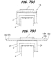
semiconductor substrate 1 may be placed on a substrate supporting/transferringtray 18 having a substrate supporting portion on its upper side, and the heat treatment may occur for thesubstrate 1 under the vacuum condition or atmospheric condition by placing the substrate supporting/transferring tray having the substrate placed thereon onto asubstrate supporting member 2 that incorporates a heating means 4 therein for heating the semiconductor substrate. - In the embodiment shown in Fig. 7 (a), the substrate supporting/transferring
tray 18 is only intended to heat thesubstrate 1 uniformly. Thus, when onesubstrate 1 for which the heating process is completed is removed from the treatment chamber (not shown) and anothersubstrate 1 is then transferred into the treatment chamber in which it is subjected to the heating process, it is impossible to use the transfer robot or the like because there is no area on the substrate supporting/transferringtray 18 that can be supported by the transfer robot. The problem is, therefore, that when the heating process is completed for thesubstrate 1, thesubstrate 1 cannot be transferred until its temperature is lowered. - In the embodiment shown in Fig. 7 (b), the substrate supporting/transferring
tray 18a has the form of a flat plate having a substrate supporting portion on its upper side, and has its outerperipheral edge 18d diametrically larger than the outerperipheral edge 2a of asubstrate supporting member 2 incorporating a heating means for heating the substrate. This is disclosed in Japanese patent application as published under H2002 - 2695. - For the substrate supporting/transferring
tray 18a shown in Fig. 7 (b), the transfer robot or the like can be used because the outerperipheral edge 18d is diametrically larger than the outerperipheral edge 2a of thesubstrate supporting member 2 that incorporates the heating means 4 for heating the substrate, wherein the transfer robot or the like can be operated for causing a pair of forks bifurcated at the forward end thereof to support the underside (bottom side in Fig. 7 (b)) of the outerperipheral edge 18c of the substrate supporting/transferringtray 18a. - When the heating process is completed for the
substrate 1, the substrate supporting/transferringtray 18a can be removed from the upper side of thesubstrate supporting member 2 of the substrate supporting/transferringtray 18a by operating the transfer robot to cause the forward ends of its pair of forks to support the underside (bottom side in Fig. 7 (b)) of the outerperipheral edge 18c of the substrate supporting/transferringtray 18a. This can be accomplished without having to wait for the temperature of thesubstrate 1 to be lowered. Then, another substrate supporting/transferringtray 18a that follows the preceding substrate supporting/transferring tray and having anew substrate 1 placed on itssubstrate supporting portion 2 may be transferred onto thesubstrate supporting member 2 within the treatment chamber where the heating process may occur for thenew substrate 1, in the same manner as described above. This permits the heating process to occur efficiently for more than one substrate in sequence. - In the embodiment shown in Fig. 7 (b) in which the substrate supporting/transferring
tray 18a in the form of the flat plate having its outerperipheral edge 18d diametrically larger than the outerperipheral edge 2a of thesubstrate supporting member 2 is placed on thesubstrate supporting member 2 incorporating the heating means 4 for heating thesubstrate 1 and the heating process occurs for thesubstrate 1 being placed on the substrate supporting/transferringtray 18a, however, it may be appreciated that heat is radiated from the outerperipheral edge side 18c of the substrate supporting/transferringtray 18a projecting beyond the outerperipheral edge 2a of thesubstrate supporting member 2. Thus, the temperature difference or non-uniform temperature distribution may occur between the center portion side and outerperipheral edge side 18c of the substrate supporting/transferringtray 18a, causing thesubstrate 1 to be heated non-uniformly during the heating process. - One object of the present invention is to provide a substrate supporting/transferring tray having a substrate (semiconductor substrate) placed on its upper side and which may be placed on a substrate supporting member, particularly a substrate supporting member incorporating a heating means therein for heating the substrate that is arranged in the treatment chamber where the heating process occurs for the substrate under the vacuum condition or atmospheric condition, wherein the substrate supporting/transferring tray allows the substrate (semiconductor substrate) to be heated more uniformly during the heating process while at the same time the substrate supporting/transferring tray can easily be removed from the substrate supporting member when the heating process is completed for the substrate, without having to wait until the temperature of the substrate is lowered, and then can be transferred from the treatment chamber into any subsequent process. Thus, the heating process can occur efficiently for more than one substrate in sequence.
- In order to attain the above object and solve the problems described above in connection with the prior art, an embodiment of the substrate supporting/transferring tray proposed by the present invention, on the upper side of which a substrate (semiconductor substrate) may be placed, may be placed on the substrate supporting member that is arranged in the treatment chamber in which the heating process occurs for the substrate, wherein the substrate supporting/transferring tray includes a disc-shaped substrate supporting portion located on its upper side, a lateral wall portion that extends downwardly from the peripheral edge of the disc-shaped substrate supporting portion and optimally an annular portion that extends radially outwardly from the bottom end side of the cylindrical lateral wall portion.
- Several advantages may be provided by the substrate supporting/transferring tray having a substrate (semiconductor substrate) placed on its upper side and which may be placed on a substrate supporting member, particularly a substrate supporting member incorporating a heating means therein for heating the substrate and which is arranged in the treatment chamber where the heating process occurs for the substrate under the vacuum condition or atmospheric condition, wherein the substrate supporting/transferring tray allows the substrate (semiconductor substrate) to be heated more uniformly during the heating process while at the same time the substrate supporting/transferring tray can easily be removed from the substrate supporting member when the heating process is completed for the substrate, without having to wait until the temperature of the substrate is lowered, and then can be transferred from the treatment chamber into any subsequent process and wherein the heating process can occur efficiently for more than one substrate in sequence.
- The following describes several preferred embodiments of the present invention by referring to the accompanying drawings.
- By first referring to Fig. 1, a first embodiment of the present invention is described.
- A
substrate supporting member 2 is arranged inside atreatment chamber 11 in which heat treatment may be performed for asubstrate 1. Thesubstrate supporting member 2 has a heater or heating means 4 incorporated therein for heating the substrate, such as a thermoelectron generator intended for heating by electron impact, an infrared lamp intended for heating by infrared rays and the like. In this way, thesubstrate 1 may be treated thermally inside thetreatment chamber 11. - The
treatment chamber 11 in which the heat treatment occurs for thesubstrate 1 may be placed internally under a specific vacuum condition or under atmospheric condition. - A substrate supporting/transferring
tray 8 is now described. The substrate supporting/transferringtray 8 may be placed on thesubstrate supporting member 2, and a substrate (a semiconductor substrate such as Si substrate, SiC substrate and the like, for example) may be placed on the upper side of the substrate supporting member. - The substrate supporting/transferring
tray 8 includes a disc-shapedsubstrate supporting portion 8e (Fig. 3 (a)) on its upper side, and a cylindricallateral wall portion 9 that extends from the peripheral edge of the disc-shapedsubstrate supporting portion 8e toward its bottom side. - As shown in Fig. 1, the cylindrical
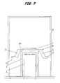
lateral wall portion 9 may be formed like a cylindrical shape that extends vertically from the peripheral edge of the disc-shaped substrate supporting portion 8c toward the bottom side (bottom end in Fig. 1) along the outer periphery of the cylindrically-shapedsubstrate supporting member 2. As an alternative form, as shown in Fig. 2, the cylindricallateral wall portion 9 may be formed like a reversed funnel shape that is becoming diametrically enlarged as it extends vertically from the peripheral edge of the disc-shapedsubstrate supporting portion 8e toward the bottom side (bottom side in Fig. 1) along the outer periphery of the cylindrically-shapedsubstrate supporting member 2. - It should be noted, however, that in order to ensure that the temperature difference that may occur between the
substrate supporting member 2 and substrate supporting/transferringtray 8 when the substrate supporting/transferringtray 8 is heated through thesubstrate supporting member 2 by the heating means 4 or the temperature distribution inside the surface of the substrate supporting/transferringtray 8 can be kept as small as possible, thereby allowing the substrate supporting/transferringtray 8 to be heated uniformly inside its surface, the cylindricallateral wall portion 9 should preferably be formed like the cylindrical shape such that it can extend from the peripheral edge of the disc-shapedsubstrate supporting portion 8e along the outer periphery of thesubstrate supporting member 8, as shown in Fig. 1. - An
annular portion 10 is provided such that it extends radially outwardly from the bottom side of the cylindricallateral wall portion 9. - The substrate supporting/transferring
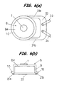
tray 8 in which thesubstrate 1 is placed on the disc-shapedsubstrate supporting portion 8e as shown in Fig. 1 may be lifted by operating a transfer robot or the like, which includes a pair ofarms forks base end 22 linked to the pair ofarms tray 8 may be transferred by operating the transfer robot to cause its pair offorks annular portion 10. - When the heating process is then completed for one
substrate 1, the substrate supporting/transferringtray 8 on which thatsubstrate 1 is placed may be removed from thesubstrate supporting member 2 by operating the transfer robot to cause its pair offorks annular portion 10 of the substrate supporting/transferringtray 8, without having to wait for the temperature of thesubstrate 1 to be lowered. Another substrate supporting/transferringtray 8 that follows the preceding substrate supporting/transferringtray 8 and having anothersubstrate 1 placed on the disc-shapedsubstrate supporting portion 8e may be transferred onto thesubstrate supporting member 2 in thetreatment chamber 11 where the heating process may begin for thenew substrate 1. In this way, the heating process can occur efficiently for more than one substrate in sequence. - It may be seen from Figs. 1 and 2 that the substrate supporting/transferring
tray 8 includes the cylindricallateral wall portion 9 extending from the peripheral edge of the disc-shapedsubstrate supporting portion 8e provided on its upper side toward the bottom side. Thus, the temperature difference that may occur between thesubstrate supporting member 2 and substrate supporting/transferringtray 8 when the substrate supporting/transferring tray is heated through thesubstrate supporting member 2 by the heating means 4 can be kept as small as possible, as compared against the prior art substrate supporting/transferringtray tray 8 may also be kept as small as possible, as compared against the prior art substrate supporting/transferringtray tray 8 of the present invention, therefore, the heating can occur more uniformly inside the surface. - In the embodiments shown in Figs. 3 and 4, the
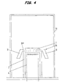
annular portion 10 is not provided, but only the cylindricallateral wall portion 9 is provided. However, this embodiment may also provide the effects that are equivalent to those of the embodiments described above. Specifically, the embodiment shown in Fig. 3 represents a variation of the embodiment shown in Fig. 1 in which noannular portion 10 is provided, but only the cylindricallateral wall portion 9 is provided. Similarly, the embodiment shown in Fig. 4 represents a variation of the embodiment shown in Fig. 2 in which noannular portion 10 is provided, but only the cylindricallateral wall portion 9 is provided. The embodiments shown in Figs. 3 and 4 would be more advantageous if theannular portion 10 is also provided as is the case for the embodiments shown in Figs. 1 and 2, since the temperature difference that may occur between thesubstrate supporting member 2 having the heating means 4 incorporated therein and the substrate supporting/transferringtray 8 can be reduced further and the temperature distribution inside the substrate supporting/transferringtray 8 can also be reduced further, thereby permitting the heating process to occur more uniformly inside the substrate supporting/transferringtray 8. - As shown in Fig. 5 (a), a
cap 5 is mounted on the substrate supporting/transferringtray 8. Thiscap 5 may be provided for covering the substrate 1 (such as SiC substrate) placed on the substrate supporting/transferringtray 8, so that it can cooperate with the substrate supporting/transferringtray 8 to seal thesubstrate 1 during the heating process. - Specifically, the
cap 5 may be provided for sealing thespace 3 in which thesubstrate 1 is placed during the heating process. More specifically, the substrate supporting/transferringtray 8 on which thesubstrate 1 is placed may be covered with thecap 5, thereby sealing thespace 3 in which thesubstrate 1 is placed during the heating process. - In this way, the
substrate 1 can be heated more efficiently because thespace 3 in which thesubstrate 1 is placed can be sealed by thecap 5 as described above during the heating process and because of the radiant heat originating from thecap 5. - The embodiment shown in Fig. 5 (b) differs from the embodiment shown in Fig. 5 (a) in that the
cap 5 has ahook step 6 on the bottom side of thelateral wall 5c that is provided for engaging the outer periphery on the upper end of the substrate supporting/transferringtray 8, with the inner diameter R2 of the lateral wall of thecap 5 where thehook step 6 is located being larger than the outer diameter R3 of the cylindricallateral wall portion 9 of the substrate supporting/transferringtray 8 by at least the plus or positive (+) tolerance. - Specifically, the substrate supporting/transferring
tray 8 shown in Fig. 5 (b) is combined with thecap 5 that may be placed on the substrate supporting portion on which thesubstrate 1 is placed so that it can seal thespace 3 in which thesubstrate 1 is placed on the substrate supporting portion, wherein thecap 5 has thehook step 6 on it bottom end side that may engage the outer periphery on the upper end of the substrate supporting portion, with the inner diameter R2 of the lateral wall of thecap 5 where thehook step 6 is located being larger than the outer diameter R3 of the cylindricallateral wall portion 9 of the substrate supporting/transferringtray 8 by at least the plus or positive (+) tolerance. - Thus, the
space 3 in which thesubstrate 1 is placed can be sealed more securely by allowing thecap 5 and substrate supporting/transferringtray 8 to expand thermally during the heating process. - The embodiment shown in Fig. 5 (c) differs from the embodiment shown in Fig. 5 (b) in that the
cap 5 has acoating layer 5b formed on the surface of thecap body 5a. - The
coating layer 5b formed on the surface of thecap body 5a serves to prevent gases from being emitted from thecap 5 or prevent materials from scattering from thecap 5, thereby protecting the internal surface of theheat chamber 11 from being polluted with such gases or materials. - The
coating layer 5b may be formed from any suitable materials that can prevent gases from being emitted from thecap body 5a, for example, pyrolytic carbons such as Pyrolytic Graphite, Pyrolytic Carbon and the like. Thecoating layer 5b should preferably be formed to have the thickness of between 10µm and 50µm. - Although the present invention has been described with reference to several preferred embodiments thereof by referring to the accompanying drawings, it should be understood that the present invention is not restricted to those embodiments, which may be modified in numerous ways without departing from the spirit and scope of the present invention as defined in the appended claims.
-
- Fig. 1 represents a cross-sectional view illustrating the substrate supporting/transferring tray according to a first embodiment of the present invention although some parts are not shown;
- Fig. 2 represents a cross-sectional view illustrating the substrate supporting/transferring tray according to a second embodiment of the present invention although some parts are not shown;
- Fig. 3 represents a cross-sectional view illustrating the substrate supporting/transferring tray according to a variation of the first embodiment of the present invention shown in Fig. 1, although some parts are not shown;
- Fig. 4 represents a cross-sectional view illustrating the substrate supporting/transferring tray according to a variation of the second embodiment of the present invention shown in Fig. 2, although some parts are not shown;
- Fig. 5 (a), (b) and (c) represent a cross-sectional view illustrating the substrate supporting/transferring tray according to a third embodiment of the present invention, although some parts are not shown;
- Fig. 6 (a) represents a plan view illustrating how the substrate supporting/transferring tray having a substrate placed thereon can be operated in accordance with an embodiment of the present invention;
- Fig. 6 (b) represents a front view illustrating how the substrate supporting/transferring tray having a substrate placed thereon can be operated in accordance with an embodiment of the present invention; and
- Fig. 7 (a) and (b) represent a cross-sectional view illustrating the substrate supporting/transferring tray according to the prior art, although some parts are not shown.
Claims (2)
- A substrate supporting/transferring tray on which a semiconductor substrate may be placed and which tray is adapted to be placed on a substrate supporting member arranged in a treatment chamber in which the heat treatment occurs for the substrate, the substrate supporting/transferring tray including:a substrate supporting portion formed in a disc-shape on an upper side of the substrate supporting/transferring tray; anda cylindrical lateral wall portion extending downwardly from a peripheral edge of the disc-shape substrate supporting portion; andan annular portion extending radially outwardly from the bottom end of said cylindrical lateral wall portion.
- The substrate supporting/transferring tray as defined in Claim 1, further including:a cap disposed on the substrate supporting portion for sealing the space in which the substrate may be placed on the upper side of the substrate supporting portion, said cap having a hooking step on its bottom end side for engaging an outer periphery on an upper end of the substrate supporting portion and having an inner diameter (R2) of its lateral wall located on the hooking step being larger than an outer diameter (R3) on the upper end of the substrate supporting portion by at least a positive tolerance.
Applications Claiming Priority (2)
| Application Number | Priority Date | Filing Date | Title |
|---|---|---|---|
| JP2004303875 | 2004-10-19 | ||
| PCT/JP2005/019091 WO2006043531A1 (en) | 2004-10-19 | 2005-10-18 | Substrate supporting/transferring tray |
Publications (2)
| Publication Number | Publication Date |
|---|---|
| EP1811559A1 true EP1811559A1 (en) | 2007-07-25 |
| EP1811559A4 EP1811559A4 (en) | 2010-04-21 |
Family
ID=36202946
Family Applications (1)
| Application Number | Title | Priority Date | Filing Date |
|---|---|---|---|
| EP05795512A Withdrawn EP1811559A4 (en) | 2004-10-19 | 2005-10-18 | SUPPORT AND SUBSTRATE TRANSFER TRAY |
Country Status (6)
| Country | Link |
|---|---|
| US (2) | US7780440B2 (en) |
| EP (1) | EP1811559A4 (en) |
| JP (1) | JP4453984B2 (en) |
| KR (1) | KR20070056154A (en) |
| CN (2) | CN101061578A (en) |
| WO (1) | WO2006043531A1 (en) |
Families Citing this family (415)
| Publication number | Priority date | Publication date | Assignee | Title |
|---|---|---|---|---|
| KR20070056154A (en) * | 2004-10-19 | 2007-05-31 | 캐논 아네르바 가부시키가이샤 | Board support and transfer tray |
| US8986456B2 (en) | 2006-10-10 | 2015-03-24 | Asm America, Inc. | Precursor delivery system |
| JP2008166729A (en) * | 2006-12-08 | 2008-07-17 | Canon Anelva Corp | Substrate heating apparatus and semiconductor manufacturing method |
| US7666763B2 (en) | 2007-05-29 | 2010-02-23 | Canon Anelva Corporation | Nanosilicon semiconductor substrate manufacturing method and semiconductor circuit device using nanosilicon semiconductor substrate manufactured by the method |
| US10378106B2 (en) | 2008-11-14 | 2019-08-13 | Asm Ip Holding B.V. | Method of forming insulation film by modified PEALD |
| US9394608B2 (en) | 2009-04-06 | 2016-07-19 | Asm America, Inc. | Semiconductor processing reactor and components thereof |
| US8877655B2 (en) | 2010-05-07 | 2014-11-04 | Asm America, Inc. | Systems and methods for thin-film deposition of metal oxides using excited nitrogen-oxygen species |
| US8802201B2 (en) | 2009-08-14 | 2014-08-12 | Asm America, Inc. | Systems and methods for thin-film deposition of metal oxides using excited nitrogen-oxygen species |
| US8883270B2 (en) | 2009-08-14 | 2014-11-11 | Asm America, Inc. | Systems and methods for thin-film deposition of metal oxides using excited nitrogen—oxygen species |
| CN102456604A (en) * | 2010-10-21 | 2012-05-16 | 北京北方微电子基地设备工艺研究中心有限责任公司 | Chuck, method of manufacturing the same, and wafer processing apparatus having the same |
| US9312155B2 (en) | 2011-06-06 | 2016-04-12 | Asm Japan K.K. | High-throughput semiconductor-processing apparatus equipped with multiple dual-chamber modules |
| US9793148B2 (en) | 2011-06-22 | 2017-10-17 | Asm Japan K.K. | Method for positioning wafers in multiple wafer transport |
| US10364496B2 (en) | 2011-06-27 | 2019-07-30 | Asm Ip Holding B.V. | Dual section module having shared and unshared mass flow controllers |
| US10854498B2 (en) | 2011-07-15 | 2020-12-01 | Asm Ip Holding B.V. | Wafer-supporting device and method for producing same |
| US20130023129A1 (en) | 2011-07-20 | 2013-01-24 | Asm America, Inc. | Pressure transmitter for a semiconductor processing environment |
| US9096931B2 (en) | 2011-10-27 | 2015-08-04 | Asm America, Inc | Deposition valve assembly and method of heating the same |
| US9341296B2 (en) | 2011-10-27 | 2016-05-17 | Asm America, Inc. | Heater jacket for a fluid line |
| US9017481B1 (en) | 2011-10-28 | 2015-04-28 | Asm America, Inc. | Process feed management for semiconductor substrate processing |
| US9167625B2 (en) | 2011-11-23 | 2015-10-20 | Asm Ip Holding B.V. | Radiation shielding for a substrate holder |
| US9005539B2 (en) | 2011-11-23 | 2015-04-14 | Asm Ip Holding B.V. | Chamber sealing member |
| US9202727B2 (en) * | 2012-03-02 | 2015-12-01 | ASM IP Holding | Susceptor heater shim |
| US8946830B2 (en) | 2012-04-04 | 2015-02-03 | Asm Ip Holdings B.V. | Metal oxide protective layer for a semiconductor device |
| US9029253B2 (en) | 2012-05-02 | 2015-05-12 | Asm Ip Holding B.V. | Phase-stabilized thin films, structures and devices including the thin films, and methods of forming same |
| US8728832B2 (en) | 2012-05-07 | 2014-05-20 | Asm Ip Holdings B.V. | Semiconductor device dielectric interface layer |
| US8933375B2 (en) | 2012-06-27 | 2015-01-13 | Asm Ip Holding B.V. | Susceptor heater and method of heating a substrate |
| US9558931B2 (en) | 2012-07-27 | 2017-01-31 | Asm Ip Holding B.V. | System and method for gas-phase sulfur passivation of a semiconductor surface |
| US9117866B2 (en) | 2012-07-31 | 2015-08-25 | Asm Ip Holding B.V. | Apparatus and method for calculating a wafer position in a processing chamber under process conditions |
| US9659799B2 (en) | 2012-08-28 | 2017-05-23 | Asm Ip Holding B.V. | Systems and methods for dynamic semiconductor process scheduling |
| US9169975B2 (en) | 2012-08-28 | 2015-10-27 | Asm Ip Holding B.V. | Systems and methods for mass flow controller verification |
| US9021985B2 (en) | 2012-09-12 | 2015-05-05 | Asm Ip Holdings B.V. | Process gas management for an inductively-coupled plasma deposition reactor |
| US9324811B2 (en) | 2012-09-26 | 2016-04-26 | Asm Ip Holding B.V. | Structures and devices including a tensile-stressed silicon arsenic layer and methods of forming same |
| US10714315B2 (en) | 2012-10-12 | 2020-07-14 | Asm Ip Holdings B.V. | Semiconductor reaction chamber showerhead |
| CN103010557B (en) * | 2012-12-18 | 2015-11-25 | 杭州中亚机械股份有限公司 | A kind of vanning bracket and arrangement method thereof |
| US9640416B2 (en) | 2012-12-26 | 2017-05-02 | Asm Ip Holding B.V. | Single-and dual-chamber module-attachable wafer-handling chamber |
| US20160376700A1 (en) | 2013-02-01 | 2016-12-29 | Asm Ip Holding B.V. | System for treatment of deposition reactor |
| US8894870B2 (en) | 2013-02-01 | 2014-11-25 | Asm Ip Holding B.V. | Multi-step method and apparatus for etching compounds containing a metal |
| US9484191B2 (en) | 2013-03-08 | 2016-11-01 | Asm Ip Holding B.V. | Pulsed remote plasma method and system |
| US9589770B2 (en) | 2013-03-08 | 2017-03-07 | Asm Ip Holding B.V. | Method and systems for in-situ formation of intermediate reactive species |
| US8993054B2 (en) | 2013-07-12 | 2015-03-31 | Asm Ip Holding B.V. | Method and system to reduce outgassing in a reaction chamber |
| US9018111B2 (en) | 2013-07-22 | 2015-04-28 | Asm Ip Holding B.V. | Semiconductor reaction chamber with plasma capabilities |
| US9396934B2 (en) | 2013-08-14 | 2016-07-19 | Asm Ip Holding B.V. | Methods of forming films including germanium tin and structures and devices including the films |
| US9793115B2 (en) | 2013-08-14 | 2017-10-17 | Asm Ip Holding B.V. | Structures and devices including germanium-tin films and methods of forming same |
| US9240412B2 (en) | 2013-09-27 | 2016-01-19 | Asm Ip Holding B.V. | Semiconductor structure and device and methods of forming same using selective epitaxial process |
| US9556516B2 (en) | 2013-10-09 | 2017-01-31 | ASM IP Holding B.V | Method for forming Ti-containing film by PEALD using TDMAT or TDEAT |
| US9605343B2 (en) | 2013-11-13 | 2017-03-28 | Asm Ip Holding B.V. | Method for forming conformal carbon films, structures conformal carbon film, and system of forming same |
| US10179947B2 (en) | 2013-11-26 | 2019-01-15 | Asm Ip Holding B.V. | Method for forming conformal nitrided, oxidized, or carbonized dielectric film by atomic layer deposition |
| US10683571B2 (en) | 2014-02-25 | 2020-06-16 | Asm Ip Holding B.V. | Gas supply manifold and method of supplying gases to chamber using same |
| US9447498B2 (en) | 2014-03-18 | 2016-09-20 | Asm Ip Holding B.V. | Method for performing uniform processing in gas system-sharing multiple reaction chambers |
| US10167557B2 (en) | 2014-03-18 | 2019-01-01 | Asm Ip Holding B.V. | Gas distribution system, reactor including the system, and methods of using the same |
| US11015245B2 (en) | 2014-03-19 | 2021-05-25 | Asm Ip Holding B.V. | Gas-phase reactor and system having exhaust plenum and components thereof |
| US9404587B2 (en) | 2014-04-24 | 2016-08-02 | ASM IP Holding B.V | Lockout tagout for semiconductor vacuum valve |
| US10858737B2 (en) | 2014-07-28 | 2020-12-08 | Asm Ip Holding B.V. | Showerhead assembly and components thereof |
| US9543180B2 (en) | 2014-08-01 | 2017-01-10 | Asm Ip Holding B.V. | Apparatus and method for transporting wafers between wafer carrier and process tool under vacuum |
| US9890456B2 (en) | 2014-08-21 | 2018-02-13 | Asm Ip Holding B.V. | Method and system for in situ formation of gas-phase compounds |
| US9657845B2 (en) | 2014-10-07 | 2017-05-23 | Asm Ip Holding B.V. | Variable conductance gas distribution apparatus and method |
| US10941490B2 (en) | 2014-10-07 | 2021-03-09 | Asm Ip Holding B.V. | Multiple temperature range susceptor, assembly, reactor and system including the susceptor, and methods of using the same |
| KR102300403B1 (en) | 2014-11-19 | 2021-09-09 | 에이에스엠 아이피 홀딩 비.브이. | Method of depositing thin film |
| KR102263121B1 (en) | 2014-12-22 | 2021-06-09 | 에이에스엠 아이피 홀딩 비.브이. | Semiconductor device and manufacuring method thereof |
| US9478415B2 (en) | 2015-02-13 | 2016-10-25 | Asm Ip Holding B.V. | Method for forming film having low resistance and shallow junction depth |
| US10529542B2 (en) | 2015-03-11 | 2020-01-07 | Asm Ip Holdings B.V. | Cross-flow reactor and method |
| US10276355B2 (en) | 2015-03-12 | 2019-04-30 | Asm Ip Holding B.V. | Multi-zone reactor, system including the reactor, and method of using the same |
| US10458018B2 (en) | 2015-06-26 | 2019-10-29 | Asm Ip Holding B.V. | Structures including metal carbide material, devices including the structures, and methods of forming same |
| US10600673B2 (en) | 2015-07-07 | 2020-03-24 | Asm Ip Holding B.V. | Magnetic susceptor to baseplate seal |
| US9899291B2 (en) | 2015-07-13 | 2018-02-20 | Asm Ip Holding B.V. | Method for protecting layer by forming hydrocarbon-based extremely thin film |
| US10043661B2 (en) | 2015-07-13 | 2018-08-07 | Asm Ip Holding B.V. | Method for protecting layer by forming hydrocarbon-based extremely thin film |
| US10083836B2 (en) | 2015-07-24 | 2018-09-25 | Asm Ip Holding B.V. | Formation of boron-doped titanium metal films with high work function |
| US10087525B2 (en) | 2015-08-04 | 2018-10-02 | Asm Ip Holding B.V. | Variable gap hard stop design |
| US9647114B2 (en) | 2015-08-14 | 2017-05-09 | Asm Ip Holding B.V. | Methods of forming highly p-type doped germanium tin films and structures and devices including the films |
| US9711345B2 (en) | 2015-08-25 | 2017-07-18 | Asm Ip Holding B.V. | Method for forming aluminum nitride-based film by PEALD |
| US9960072B2 (en) | 2015-09-29 | 2018-05-01 | Asm Ip Holding B.V. | Variable adjustment for precise matching of multiple chamber cavity housings |
| US9909214B2 (en) | 2015-10-15 | 2018-03-06 | Asm Ip Holding B.V. | Method for depositing dielectric film in trenches by PEALD |
| US10211308B2 (en) | 2015-10-21 | 2019-02-19 | Asm Ip Holding B.V. | NbMC layers |
| US10322384B2 (en) | 2015-11-09 | 2019-06-18 | Asm Ip Holding B.V. | Counter flow mixer for process chamber |
| US9455138B1 (en) | 2015-11-10 | 2016-09-27 | Asm Ip Holding B.V. | Method for forming dielectric film in trenches by PEALD using H-containing gas |
| US9905420B2 (en) | 2015-12-01 | 2018-02-27 | Asm Ip Holding B.V. | Methods of forming silicon germanium tin films and structures and devices including the films |
| US9607837B1 (en) | 2015-12-21 | 2017-03-28 | Asm Ip Holding B.V. | Method for forming silicon oxide cap layer for solid state diffusion process |
| US9627221B1 (en) | 2015-12-28 | 2017-04-18 | Asm Ip Holding B.V. | Continuous process incorporating atomic layer etching |
| US9735024B2 (en) | 2015-12-28 | 2017-08-15 | Asm Ip Holding B.V. | Method of atomic layer etching using functional group-containing fluorocarbon |
| US11139308B2 (en) | 2015-12-29 | 2021-10-05 | Asm Ip Holding B.V. | Atomic layer deposition of III-V compounds to form V-NAND devices |
| US10468251B2 (en) | 2016-02-19 | 2019-11-05 | Asm Ip Holding B.V. | Method for forming spacers using silicon nitride film for spacer-defined multiple patterning |
| US10529554B2 (en) | 2016-02-19 | 2020-01-07 | Asm Ip Holding B.V. | Method for forming silicon nitride film selectively on sidewalls or flat surfaces of trenches |
| US9754779B1 (en) | 2016-02-19 | 2017-09-05 | Asm Ip Holding B.V. | Method for forming silicon nitride film selectively on sidewalls or flat surfaces of trenches |
| US10501866B2 (en) | 2016-03-09 | 2019-12-10 | Asm Ip Holding B.V. | Gas distribution apparatus for improved film uniformity in an epitaxial system |
| US10343920B2 (en) | 2016-03-18 | 2019-07-09 | Asm Ip Holding B.V. | Aligned carbon nanotubes |
| US9892913B2 (en) | 2016-03-24 | 2018-02-13 | Asm Ip Holding B.V. | Radial and thickness control via biased multi-port injection settings |
| US10865475B2 (en) | 2016-04-21 | 2020-12-15 | Asm Ip Holding B.V. | Deposition of metal borides and silicides |
| US10190213B2 (en) | 2016-04-21 | 2019-01-29 | Asm Ip Holding B.V. | Deposition of metal borides |
| US10087522B2 (en) | 2016-04-21 | 2018-10-02 | Asm Ip Holding B.V. | Deposition of metal borides |
| US10367080B2 (en) | 2016-05-02 | 2019-07-30 | Asm Ip Holding B.V. | Method of forming a germanium oxynitride film |
| US10032628B2 (en) | 2016-05-02 | 2018-07-24 | Asm Ip Holding B.V. | Source/drain performance through conformal solid state doping |
| KR102592471B1 (en) | 2016-05-17 | 2023-10-20 | 에이에스엠 아이피 홀딩 비.브이. | Method of forming metal interconnection and method of fabricating semiconductor device using the same |
| US11453943B2 (en) | 2016-05-25 | 2022-09-27 | Asm Ip Holding B.V. | Method for forming carbon-containing silicon/metal oxide or nitride film by ALD using silicon precursor and hydrocarbon precursor |
| US10388509B2 (en) | 2016-06-28 | 2019-08-20 | Asm Ip Holding B.V. | Formation of epitaxial layers via dislocation filtering |
| US9859151B1 (en) | 2016-07-08 | 2018-01-02 | Asm Ip Holding B.V. | Selective film deposition method to form air gaps |
| US10612137B2 (en) | 2016-07-08 | 2020-04-07 | Asm Ip Holdings B.V. | Organic reactants for atomic layer deposition |
| US9793135B1 (en) | 2016-07-14 | 2017-10-17 | ASM IP Holding B.V | Method of cyclic dry etching using etchant film |
| US10714385B2 (en) | 2016-07-19 | 2020-07-14 | Asm Ip Holding B.V. | Selective deposition of tungsten |
| US10381226B2 (en) | 2016-07-27 | 2019-08-13 | Asm Ip Holding B.V. | Method of processing substrate |
| US9812320B1 (en) | 2016-07-28 | 2017-11-07 | Asm Ip Holding B.V. | Method and apparatus for filling a gap |
| KR102532607B1 (en) | 2016-07-28 | 2023-05-15 | 에이에스엠 아이피 홀딩 비.브이. | Substrate processing apparatus and method of operating the same |
| US10395919B2 (en) | 2016-07-28 | 2019-08-27 | Asm Ip Holding B.V. | Method and apparatus for filling a gap |
| US9887082B1 (en) | 2016-07-28 | 2018-02-06 | Asm Ip Holding B.V. | Method and apparatus for filling a gap |
| US10177025B2 (en) | 2016-07-28 | 2019-01-08 | Asm Ip Holding B.V. | Method and apparatus for filling a gap |
| US10090316B2 (en) | 2016-09-01 | 2018-10-02 | Asm Ip Holding B.V. | 3D stacked multilayer semiconductor memory using doped select transistor channel |
| US10410943B2 (en) | 2016-10-13 | 2019-09-10 | Asm Ip Holding B.V. | Method for passivating a surface of a semiconductor and related systems |
| US10643826B2 (en) | 2016-10-26 | 2020-05-05 | Asm Ip Holdings B.V. | Methods for thermally calibrating reaction chambers |
| US11532757B2 (en) | 2016-10-27 | 2022-12-20 | Asm Ip Holding B.V. | Deposition of charge trapping layers |
| US10435790B2 (en) | 2016-11-01 | 2019-10-08 | Asm Ip Holding B.V. | Method of subatmospheric plasma-enhanced ALD using capacitively coupled electrodes with narrow gap |
| US10714350B2 (en) | 2016-11-01 | 2020-07-14 | ASM IP Holdings, B.V. | Methods for forming a transition metal niobium nitride film on a substrate by atomic layer deposition and related semiconductor device structures |
| US10643904B2 (en) | 2016-11-01 | 2020-05-05 | Asm Ip Holdings B.V. | Methods for forming a semiconductor device and related semiconductor device structures |
| US10229833B2 (en) | 2016-11-01 | 2019-03-12 | Asm Ip Holding B.V. | Methods for forming a transition metal nitride film on a substrate by atomic layer deposition and related semiconductor device structures |
| US10134757B2 (en) | 2016-11-07 | 2018-11-20 | Asm Ip Holding B.V. | Method of processing a substrate and a device manufactured by using the method |
| KR102546317B1 (en) | 2016-11-15 | 2023-06-21 | 에이에스엠 아이피 홀딩 비.브이. | Gas supply unit and substrate processing apparatus including the same |
| US10340135B2 (en) | 2016-11-28 | 2019-07-02 | Asm Ip Holding B.V. | Method of topologically restricted plasma-enhanced cyclic deposition of silicon or metal nitride |
| KR102762543B1 (en) | 2016-12-14 | 2025-02-05 | 에이에스엠 아이피 홀딩 비.브이. | Substrate processing apparatus |
| US11447861B2 (en) | 2016-12-15 | 2022-09-20 | Asm Ip Holding B.V. | Sequential infiltration synthesis apparatus and a method of forming a patterned structure |
| US11581186B2 (en) | 2016-12-15 | 2023-02-14 | Asm Ip Holding B.V. | Sequential infiltration synthesis apparatus |
| US9916980B1 (en) | 2016-12-15 | 2018-03-13 | Asm Ip Holding B.V. | Method of forming a structure on a substrate |
| KR102700194B1 (en) | 2016-12-19 | 2024-08-28 | 에이에스엠 아이피 홀딩 비.브이. | Substrate processing apparatus |
| US10269558B2 (en) | 2016-12-22 | 2019-04-23 | Asm Ip Holding B.V. | Method of forming a structure on a substrate |
| US10867788B2 (en) | 2016-12-28 | 2020-12-15 | Asm Ip Holding B.V. | Method of forming a structure on a substrate |
| US11390950B2 (en) | 2017-01-10 | 2022-07-19 | Asm Ip Holding B.V. | Reactor system and method to reduce residue buildup during a film deposition process |
| US10655221B2 (en) | 2017-02-09 | 2020-05-19 | Asm Ip Holding B.V. | Method for depositing oxide film by thermal ALD and PEALD |
| US10468261B2 (en) | 2017-02-15 | 2019-11-05 | Asm Ip Holding B.V. | Methods for forming a metallic film on a substrate by cyclical deposition and related semiconductor device structures |
| US10529563B2 (en) | 2017-03-29 | 2020-01-07 | Asm Ip Holdings B.V. | Method for forming doped metal oxide films on a substrate by cyclical deposition and related semiconductor device structures |
| US10283353B2 (en) | 2017-03-29 | 2019-05-07 | Asm Ip Holding B.V. | Method of reforming insulating film deposited on substrate with recess pattern |
| US10103040B1 (en) | 2017-03-31 | 2018-10-16 | Asm Ip Holding B.V. | Apparatus and method for manufacturing a semiconductor device |
| USD830981S1 (en) | 2017-04-07 | 2018-10-16 | Asm Ip Holding B.V. | Susceptor for semiconductor substrate processing apparatus |
| KR102457289B1 (en) | 2017-04-25 | 2022-10-21 | 에이에스엠 아이피 홀딩 비.브이. | Method for depositing a thin film and manufacturing a semiconductor device |
| US10892156B2 (en) | 2017-05-08 | 2021-01-12 | Asm Ip Holding B.V. | Methods for forming a silicon nitride film on a substrate and related semiconductor device structures |
| US10446393B2 (en) | 2017-05-08 | 2019-10-15 | Asm Ip Holding B.V. | Methods for forming silicon-containing epitaxial layers and related semiconductor device structures |
| US10770286B2 (en) | 2017-05-08 | 2020-09-08 | Asm Ip Holdings B.V. | Methods for selectively forming a silicon nitride film on a substrate and related semiconductor device structures |
| US10504742B2 (en) | 2017-05-31 | 2019-12-10 | Asm Ip Holding B.V. | Method of atomic layer etching using hydrogen plasma |
| US10886123B2 (en) | 2017-06-02 | 2021-01-05 | Asm Ip Holding B.V. | Methods for forming low temperature semiconductor layers and related semiconductor device structures |
| US12040200B2 (en) | 2017-06-20 | 2024-07-16 | Asm Ip Holding B.V. | Semiconductor processing apparatus and methods for calibrating a semiconductor processing apparatus |
| US11306395B2 (en) | 2017-06-28 | 2022-04-19 | Asm Ip Holding B.V. | Methods for depositing a transition metal nitride film on a substrate by atomic layer deposition and related deposition apparatus |
| US10685834B2 (en) | 2017-07-05 | 2020-06-16 | Asm Ip Holdings B.V. | Methods for forming a silicon germanium tin layer and related semiconductor device structures |
| KR20190009245A (en) | 2017-07-18 | 2019-01-28 | 에이에스엠 아이피 홀딩 비.브이. | Methods for forming a semiconductor device structure and related semiconductor device structures |
| US11018002B2 (en) | 2017-07-19 | 2021-05-25 | Asm Ip Holding B.V. | Method for selectively depositing a Group IV semiconductor and related semiconductor device structures |
| US11374112B2 (en) | 2017-07-19 | 2022-06-28 | Asm Ip Holding B.V. | Method for depositing a group IV semiconductor and related semiconductor device structures |
| US10541333B2 (en) | 2017-07-19 | 2020-01-21 | Asm Ip Holding B.V. | Method for depositing a group IV semiconductor and related semiconductor device structures |
| US10605530B2 (en) | 2017-07-26 | 2020-03-31 | Asm Ip Holding B.V. | Assembly of a liner and a flange for a vertical furnace as well as the liner and the vertical furnace |
| US10312055B2 (en) | 2017-07-26 | 2019-06-04 | Asm Ip Holding B.V. | Method of depositing film by PEALD using negative bias |
| US10590535B2 (en) | 2017-07-26 | 2020-03-17 | Asm Ip Holdings B.V. | Chemical treatment, deposition and/or infiltration apparatus and method for using the same |
| TWI815813B (en) | 2017-08-04 | 2023-09-21 | 荷蘭商Asm智慧財產控股公司 | Showerhead assembly for distributing a gas within a reaction chamber |
| US10770336B2 (en) | 2017-08-08 | 2020-09-08 | Asm Ip Holding B.V. | Substrate lift mechanism and reactor including same |
| US10692741B2 (en) | 2017-08-08 | 2020-06-23 | Asm Ip Holdings B.V. | Radiation shield |
| US10249524B2 (en) | 2017-08-09 | 2019-04-02 | Asm Ip Holding B.V. | Cassette holder assembly for a substrate cassette and holding member for use in such assembly |
| US11139191B2 (en) | 2017-08-09 | 2021-10-05 | Asm Ip Holding B.V. | Storage apparatus for storing cassettes for substrates and processing apparatus equipped therewith |
| US11769682B2 (en) | 2017-08-09 | 2023-09-26 | Asm Ip Holding B.V. | Storage apparatus for storing cassettes for substrates and processing apparatus equipped therewith |
| US10236177B1 (en) | 2017-08-22 | 2019-03-19 | ASM IP Holding B.V.. | Methods for depositing a doped germanium tin semiconductor and related semiconductor device structures |
| USD900036S1 (en) | 2017-08-24 | 2020-10-27 | Asm Ip Holding B.V. | Heater electrical connector and adapter |
| US11830730B2 (en) | 2017-08-29 | 2023-11-28 | Asm Ip Holding B.V. | Layer forming method and apparatus |
| KR102491945B1 (en) | 2017-08-30 | 2023-01-26 | 에이에스엠 아이피 홀딩 비.브이. | Substrate processing apparatus |
| US11295980B2 (en) | 2017-08-30 | 2022-04-05 | Asm Ip Holding B.V. | Methods for depositing a molybdenum metal film over a dielectric surface of a substrate by a cyclical deposition process and related semiconductor device structures |
| US11056344B2 (en) | 2017-08-30 | 2021-07-06 | Asm Ip Holding B.V. | Layer forming method |
| KR102401446B1 (en) | 2017-08-31 | 2022-05-24 | 에이에스엠 아이피 홀딩 비.브이. | Substrate processing apparatus |
| US10607895B2 (en) | 2017-09-18 | 2020-03-31 | Asm Ip Holdings B.V. | Method for forming a semiconductor device structure comprising a gate fill metal |
| KR102630301B1 (en) | 2017-09-21 | 2024-01-29 | 에이에스엠 아이피 홀딩 비.브이. | Method of sequential infiltration synthesis treatment of infiltrateable material and structures and devices formed using same |
| US10844484B2 (en) | 2017-09-22 | 2020-11-24 | Asm Ip Holding B.V. | Apparatus for dispensing a vapor phase reactant to a reaction chamber and related methods |
| US10658205B2 (en) | 2017-09-28 | 2020-05-19 | Asm Ip Holdings B.V. | Chemical dispensing apparatus and methods for dispensing a chemical to a reaction chamber |
| US10403504B2 (en) | 2017-10-05 | 2019-09-03 | Asm Ip Holding B.V. | Method for selectively depositing a metallic film on a substrate |
| US10319588B2 (en) | 2017-10-10 | 2019-06-11 | Asm Ip Holding B.V. | Method for depositing a metal chalcogenide on a substrate by cyclical deposition |
| US10923344B2 (en) | 2017-10-30 | 2021-02-16 | Asm Ip Holding B.V. | Methods for forming a semiconductor structure and related semiconductor structures |
| KR102443047B1 (en) | 2017-11-16 | 2022-09-14 | 에이에스엠 아이피 홀딩 비.브이. | Substrate processing apparatus method and apparatus manufactured thereby |
| US10910262B2 (en) | 2017-11-16 | 2021-02-02 | Asm Ip Holding B.V. | Method of selectively depositing a capping layer structure on a semiconductor device structure |
| US11022879B2 (en) | 2017-11-24 | 2021-06-01 | Asm Ip Holding B.V. | Method of forming an enhanced unexposed photoresist layer |
| TWI791689B (en) | 2017-11-27 | 2023-02-11 | 荷蘭商Asm智慧財產控股私人有限公司 | Apparatus including a clean mini environment |
| JP7214724B2 (en) | 2017-11-27 | 2023-01-30 | エーエスエム アイピー ホールディング ビー.ブイ. | Storage device for storing wafer cassettes used in batch furnaces |
| US10290508B1 (en) | 2017-12-05 | 2019-05-14 | Asm Ip Holding B.V. | Method for forming vertical spacers for spacer-defined patterning |
| US10872771B2 (en) | 2018-01-16 | 2020-12-22 | Asm Ip Holding B. V. | Method for depositing a material film on a substrate within a reaction chamber by a cyclical deposition process and related device structures |
| TWI799494B (en) | 2018-01-19 | 2023-04-21 | 荷蘭商Asm 智慧財產控股公司 | Deposition method |
| KR102695659B1 (en) | 2018-01-19 | 2024-08-14 | 에이에스엠 아이피 홀딩 비.브이. | Method for depositing a gap filling layer by plasma assisted deposition |
| USD903477S1 (en) | 2018-01-24 | 2020-12-01 | Asm Ip Holdings B.V. | Metal clamp |
| US11018047B2 (en) | 2018-01-25 | 2021-05-25 | Asm Ip Holding B.V. | Hybrid lift pin |
| US10535516B2 (en) | 2018-02-01 | 2020-01-14 | Asm Ip Holdings B.V. | Method for depositing a semiconductor structure on a surface of a substrate and related semiconductor structures |
| USD880437S1 (en) | 2018-02-01 | 2020-04-07 | Asm Ip Holding B.V. | Gas supply plate for semiconductor manufacturing apparatus |
| US11081345B2 (en) | 2018-02-06 | 2021-08-03 | Asm Ip Holding B.V. | Method of post-deposition treatment for silicon oxide film |
| US10896820B2 (en) | 2018-02-14 | 2021-01-19 | Asm Ip Holding B.V. | Method for depositing a ruthenium-containing film on a substrate by a cyclical deposition process |
| US11685991B2 (en) | 2018-02-14 | 2023-06-27 | Asm Ip Holding B.V. | Method for depositing a ruthenium-containing film on a substrate by a cyclical deposition process |
| US10731249B2 (en) | 2018-02-15 | 2020-08-04 | Asm Ip Holding B.V. | Method of forming a transition metal containing film on a substrate by a cyclical deposition process, a method for supplying a transition metal halide compound to a reaction chamber, and related vapor deposition apparatus |
| US10658181B2 (en) | 2018-02-20 | 2020-05-19 | Asm Ip Holding B.V. | Method of spacer-defined direct patterning in semiconductor fabrication |
| KR102636427B1 (en) | 2018-02-20 | 2024-02-13 | 에이에스엠 아이피 홀딩 비.브이. | Substrate processing method and apparatus |
| US10975470B2 (en) | 2018-02-23 | 2021-04-13 | Asm Ip Holding B.V. | Apparatus for detecting or monitoring for a chemical precursor in a high temperature environment |
| US11473195B2 (en) | 2018-03-01 | 2022-10-18 | Asm Ip Holding B.V. | Semiconductor processing apparatus and a method for processing a substrate |
| US11629406B2 (en) | 2018-03-09 | 2023-04-18 | Asm Ip Holding B.V. | Semiconductor processing apparatus comprising one or more pyrometers for measuring a temperature of a substrate during transfer of the substrate |
| US11114283B2 (en) | 2018-03-16 | 2021-09-07 | Asm Ip Holding B.V. | Reactor, system including the reactor, and methods of manufacturing and using same |
| KR102646467B1 (en) | 2018-03-27 | 2024-03-11 | 에이에스엠 아이피 홀딩 비.브이. | Method of forming an electrode on a substrate and a semiconductor device structure including an electrode |
| US10510536B2 (en) | 2018-03-29 | 2019-12-17 | Asm Ip Holding B.V. | Method of depositing a co-doped polysilicon film on a surface of a substrate within a reaction chamber |
| US11088002B2 (en) | 2018-03-29 | 2021-08-10 | Asm Ip Holding B.V. | Substrate rack and a substrate processing system and method |
| US11230766B2 (en) | 2018-03-29 | 2022-01-25 | Asm Ip Holding B.V. | Substrate processing apparatus and method |
| KR102501472B1 (en) | 2018-03-30 | 2023-02-20 | 에이에스엠 아이피 홀딩 비.브이. | Substrate processing method |
| KR102600229B1 (en) | 2018-04-09 | 2023-11-10 | 에이에스엠 아이피 홀딩 비.브이. | Substrate supporting device, substrate processing apparatus including the same and substrate processing method |
| US12025484B2 (en) | 2018-05-08 | 2024-07-02 | Asm Ip Holding B.V. | Thin film forming method |
| TWI843623B (en) | 2018-05-08 | 2024-05-21 | 荷蘭商Asm Ip私人控股有限公司 | Methods for depositing an oxide film on a substrate by a cyclical deposition process and related device structures |
| US12272527B2 (en) | 2018-05-09 | 2025-04-08 | Asm Ip Holding B.V. | Apparatus for use with hydrogen radicals and method of using same |
| KR20190129718A (en) | 2018-05-11 | 2019-11-20 | 에이에스엠 아이피 홀딩 비.브이. | Methods for forming a doped metal carbide film on a substrate and related semiconductor device structures |
| KR102596988B1 (en) | 2018-05-28 | 2023-10-31 | 에이에스엠 아이피 홀딩 비.브이. | Method of processing a substrate and a device manufactured by the same |
| US11718913B2 (en) | 2018-06-04 | 2023-08-08 | Asm Ip Holding B.V. | Gas distribution system and reactor system including same |
| TWI840362B (en) | 2018-06-04 | 2024-05-01 | 荷蘭商Asm Ip私人控股有限公司 | Wafer handling chamber with moisture reduction |
| US11286562B2 (en) | 2018-06-08 | 2022-03-29 | Asm Ip Holding B.V. | Gas-phase chemical reactor and method of using same |
| KR102568797B1 (en) | 2018-06-21 | 2023-08-21 | 에이에스엠 아이피 홀딩 비.브이. | Substrate processing system |
| US10797133B2 (en) | 2018-06-21 | 2020-10-06 | Asm Ip Holding B.V. | Method for depositing a phosphorus doped silicon arsenide film and related semiconductor device structures |
| TWI871083B (en) | 2018-06-27 | 2025-01-21 | 荷蘭商Asm Ip私人控股有限公司 | Cyclic deposition processes for forming metal-containing material |
| US11499222B2 (en) | 2018-06-27 | 2022-11-15 | Asm Ip Holding B.V. | Cyclic deposition methods for forming metal-containing material and films and structures including the metal-containing material |
| US10612136B2 (en) | 2018-06-29 | 2020-04-07 | ASM IP Holding, B.V. | Temperature-controlled flange and reactor system including same |
| KR102686758B1 (en) | 2018-06-29 | 2024-07-18 | 에이에스엠 아이피 홀딩 비.브이. | Method for depositing a thin film and manufacturing a semiconductor device |
| US10755922B2 (en) | 2018-07-03 | 2020-08-25 | Asm Ip Holding B.V. | Method for depositing silicon-free carbon-containing film as gap-fill layer by pulse plasma-assisted deposition |
| US10388513B1 (en) | 2018-07-03 | 2019-08-20 | Asm Ip Holding B.V. | Method for depositing silicon-free carbon-containing film as gap-fill layer by pulse plasma-assisted deposition |
| US10767789B2 (en) | 2018-07-16 | 2020-09-08 | Asm Ip Holding B.V. | Diaphragm valves, valve components, and methods for forming valve components |
| US10483099B1 (en) | 2018-07-26 | 2019-11-19 | Asm Ip Holding B.V. | Method for forming thermally stable organosilicon polymer film |
| US11053591B2 (en) | 2018-08-06 | 2021-07-06 | Asm Ip Holding B.V. | Multi-port gas injection system and reactor system including same |
| US10883175B2 (en) | 2018-08-09 | 2021-01-05 | Asm Ip Holding B.V. | Vertical furnace for processing substrates and a liner for use therein |
| US10829852B2 (en) | 2018-08-16 | 2020-11-10 | Asm Ip Holding B.V. | Gas distribution device for a wafer processing apparatus |
| US11430674B2 (en) | 2018-08-22 | 2022-08-30 | Asm Ip Holding B.V. | Sensor array, apparatus for dispensing a vapor phase reactant to a reaction chamber and related methods |
| KR102707956B1 (en) | 2018-09-11 | 2024-09-19 | 에이에스엠 아이피 홀딩 비.브이. | Method for deposition of a thin film |
| US11024523B2 (en) | 2018-09-11 | 2021-06-01 | Asm Ip Holding B.V. | Substrate processing apparatus and method |
| US11049751B2 (en) | 2018-09-14 | 2021-06-29 | Asm Ip Holding B.V. | Cassette supply system to store and handle cassettes and processing apparatus equipped therewith |
| CN110970344B (en) | 2018-10-01 | 2024-10-25 | Asmip控股有限公司 | Substrate holding device, system including the same and method of using the same |
| US11232963B2 (en) | 2018-10-03 | 2022-01-25 | Asm Ip Holding B.V. | Substrate processing apparatus and method |
| KR102592699B1 (en) | 2018-10-08 | 2023-10-23 | 에이에스엠 아이피 홀딩 비.브이. | Substrate support unit and apparatuses for depositing thin film and processing the substrate including the same |
| US10847365B2 (en) | 2018-10-11 | 2020-11-24 | Asm Ip Holding B.V. | Method of forming conformal silicon carbide film by cyclic CVD |
| US10811256B2 (en) | 2018-10-16 | 2020-10-20 | Asm Ip Holding B.V. | Method for etching a carbon-containing feature |
| KR102605121B1 (en) | 2018-10-19 | 2023-11-23 | 에이에스엠 아이피 홀딩 비.브이. | Substrate processing apparatus and substrate processing method |
| KR102546322B1 (en) | 2018-10-19 | 2023-06-21 | 에이에스엠 아이피 홀딩 비.브이. | Substrate processing apparatus and substrate processing method |
| USD948463S1 (en) | 2018-10-24 | 2022-04-12 | Asm Ip Holding B.V. | Susceptor for semiconductor substrate supporting apparatus |
| US10381219B1 (en) | 2018-10-25 | 2019-08-13 | Asm Ip Holding B.V. | Methods for forming a silicon nitride film |
| US12378665B2 (en) | 2018-10-26 | 2025-08-05 | Asm Ip Holding B.V. | High temperature coatings for a preclean and etch apparatus and related methods |
| US11087997B2 (en) | 2018-10-31 | 2021-08-10 | Asm Ip Holding B.V. | Substrate processing apparatus for processing substrates |
| KR102748291B1 (en) | 2018-11-02 | 2024-12-31 | 에이에스엠 아이피 홀딩 비.브이. | Substrate support unit and substrate processing apparatus including the same |
| US11572620B2 (en) | 2018-11-06 | 2023-02-07 | Asm Ip Holding B.V. | Methods for selectively depositing an amorphous silicon film on a substrate |
| US11031242B2 (en) | 2018-11-07 | 2021-06-08 | Asm Ip Holding B.V. | Methods for depositing a boron doped silicon germanium film |
| US10818758B2 (en) | 2018-11-16 | 2020-10-27 | Asm Ip Holding B.V. | Methods for forming a metal silicate film on a substrate in a reaction chamber and related semiconductor device structures |
| US10847366B2 (en) | 2018-11-16 | 2020-11-24 | Asm Ip Holding B.V. | Methods for depositing a transition metal chalcogenide film on a substrate by a cyclical deposition process |
| US10559458B1 (en) | 2018-11-26 | 2020-02-11 | Asm Ip Holding B.V. | Method of forming oxynitride film |
| US12040199B2 (en) | 2018-11-28 | 2024-07-16 | Asm Ip Holding B.V. | Substrate processing apparatus for processing substrates |
| US11217444B2 (en) | 2018-11-30 | 2022-01-04 | Asm Ip Holding B.V. | Method for forming an ultraviolet radiation responsive metal oxide-containing film |
| KR102636428B1 (en) | 2018-12-04 | 2024-02-13 | 에이에스엠 아이피 홀딩 비.브이. | A method for cleaning a substrate processing apparatus |
| US11158513B2 (en) | 2018-12-13 | 2021-10-26 | Asm Ip Holding B.V. | Methods for forming a rhenium-containing film on a substrate by a cyclical deposition process and related semiconductor device structures |
| JP7504584B2 (en) | 2018-12-14 | 2024-06-24 | エーエスエム・アイピー・ホールディング・ベー・フェー | Method and system for forming device structures using selective deposition of gallium nitride - Patents.com |
| TWI866480B (en) | 2019-01-17 | 2024-12-11 | 荷蘭商Asm Ip 私人控股有限公司 | Methods of forming a transition metal containing film on a substrate by a cyclical deposition process |
| KR102727227B1 (en) | 2019-01-22 | 2024-11-07 | 에이에스엠 아이피 홀딩 비.브이. | Semiconductor processing device |
| CN111524788B (en) | 2019-02-01 | 2023-11-24 | Asm Ip私人控股有限公司 | Method for forming topologically selective films of silicon oxide |
| TWI873122B (en) | 2019-02-20 | 2025-02-21 | 荷蘭商Asm Ip私人控股有限公司 | Method of filling a recess formed within a surface of a substrate, semiconductor structure formed according to the method, and semiconductor processing apparatus |
| KR20200102357A (en) | 2019-02-20 | 2020-08-31 | 에이에스엠 아이피 홀딩 비.브이. | Apparatus and methods for plug fill deposition in 3-d nand applications |
| KR102626263B1 (en) | 2019-02-20 | 2024-01-16 | 에이에스엠 아이피 홀딩 비.브이. | Cyclical deposition method including treatment step and apparatus for same |
| TWI845607B (en) | 2019-02-20 | 2024-06-21 | 荷蘭商Asm Ip私人控股有限公司 | Cyclical deposition method and apparatus for filling a recess formed within a substrate surface |
| TWI842826B (en) | 2019-02-22 | 2024-05-21 | 荷蘭商Asm Ip私人控股有限公司 | Substrate processing apparatus and method for processing substrate |
| KR102762833B1 (en) | 2019-03-08 | 2025-02-04 | 에이에스엠 아이피 홀딩 비.브이. | STRUCTURE INCLUDING SiOCN LAYER AND METHOD OF FORMING SAME |
| KR102782593B1 (en) | 2019-03-08 | 2025-03-14 | 에이에스엠 아이피 홀딩 비.브이. | Structure Including SiOC Layer and Method of Forming Same |
| KR102858005B1 (en) | 2019-03-08 | 2025-09-09 | 에이에스엠 아이피 홀딩 비.브이. | Method for Selective Deposition of Silicon Nitride Layer and Structure Including Selectively-Deposited Silicon Nitride Layer |
| JP2020167398A (en) | 2019-03-28 | 2020-10-08 | エーエスエム・アイピー・ホールディング・ベー・フェー | Door openers and substrate processing equipment provided with door openers |
| KR102809999B1 (en) | 2019-04-01 | 2025-05-19 | 에이에스엠 아이피 홀딩 비.브이. | Method of manufacturing semiconductor device |
| KR102897355B1 (en) | 2019-04-19 | 2025-12-08 | 에이에스엠 아이피 홀딩 비.브이. | Layer forming method and apparatus |
| KR20200125453A (en) | 2019-04-24 | 2020-11-04 | 에이에스엠 아이피 홀딩 비.브이. | Gas-phase reactor system and method of using same |
| KR102929471B1 (en) | 2019-05-07 | 2026-02-20 | 에이에스엠 아이피 홀딩 비.브이. | Chemical source vessel with dip tube |
| KR102869364B1 (en) | 2019-05-07 | 2025-10-10 | 에이에스엠 아이피 홀딩 비.브이. | Method for Reforming Amorphous Carbon Polymer Film |
| KR102929472B1 (en) | 2019-05-10 | 2026-02-20 | 에이에스엠 아이피 홀딩 비.브이. | Method of depositing material onto a surface and structure formed according to the method |
| JP7612342B2 (en) | 2019-05-16 | 2025-01-14 | エーエスエム・アイピー・ホールディング・ベー・フェー | Wafer boat handling apparatus, vertical batch furnace and method |
| JP7598201B2 (en) | 2019-05-16 | 2024-12-11 | エーエスエム・アイピー・ホールディング・ベー・フェー | Wafer boat handling apparatus, vertical batch furnace and method |
| USD947913S1 (en) | 2019-05-17 | 2022-04-05 | Asm Ip Holding B.V. | Susceptor shaft |
| USD975665S1 (en) | 2019-05-17 | 2023-01-17 | Asm Ip Holding B.V. | Susceptor shaft |
| USD935572S1 (en) | 2019-05-24 | 2021-11-09 | Asm Ip Holding B.V. | Gas channel plate |
| USD922229S1 (en) | 2019-06-05 | 2021-06-15 | Asm Ip Holding B.V. | Device for controlling a temperature of a gas supply unit |
| KR20200141002A (en) | 2019-06-06 | 2020-12-17 | 에이에스엠 아이피 홀딩 비.브이. | Method of using a gas-phase reactor system including analyzing exhausted gas |
| KR102918757B1 (en) | 2019-06-10 | 2026-01-28 | 에이에스엠 아이피 홀딩 비.브이. | Method for cleaning quartz epitaxial chambers |
| KR20200143254A (en) | 2019-06-11 | 2020-12-23 | 에이에스엠 아이피 홀딩 비.브이. | Method of forming an electronic structure using an reforming gas, system for performing the method, and structure formed using the method |
| USD944946S1 (en) | 2019-06-14 | 2022-03-01 | Asm Ip Holding B.V. | Shower plate |
| USD931978S1 (en) | 2019-06-27 | 2021-09-28 | Asm Ip Holding B.V. | Showerhead vacuum transport |
| KR102911421B1 (en) | 2019-07-03 | 2026-01-12 | 에이에스엠 아이피 홀딩 비.브이. | Temperature control assembly for substrate processing apparatus and method of using same |
| JP7499079B2 (en) | 2019-07-09 | 2024-06-13 | エーエスエム・アイピー・ホールディング・ベー・フェー | Plasma device using coaxial waveguide and substrate processing method |
| CN112216646B (en) | 2019-07-10 | 2026-02-10 | Asmip私人控股有限公司 | Substrate support assembly and substrate processing apparatus including the thereof |
| KR102895115B1 (en) | 2019-07-16 | 2025-12-03 | 에이에스엠 아이피 홀딩 비.브이. | Substrate processing apparatus |
| TWI826704B (en) | 2019-07-17 | 2023-12-21 | 荷蘭商Asm Ip私人控股有限公司 | Radical assist ignition plasma system and method |
| KR102860110B1 (en) | 2019-07-17 | 2025-09-16 | 에이에스엠 아이피 홀딩 비.브이. | Methods of forming silicon germanium structures |
| US11643724B2 (en) | 2019-07-18 | 2023-05-09 | Asm Ip Holding B.V. | Method of forming structures using a neutral beam |
| KR102903090B1 (en) | 2019-07-19 | 2025-12-19 | 에이에스엠 아이피 홀딩 비.브이. | Method of Forming Topology-Controlled Amorphous Carbon Polymer Film |
| TWI839544B (en) | 2019-07-19 | 2024-04-21 | 荷蘭商Asm Ip私人控股有限公司 | Method of forming topology-controlled amorphous carbon polymer film |
| EP3769909B1 (en) * | 2019-07-25 | 2025-12-10 | Maschinenfabrik Berthold Hermle AG | Workpiece pallet and machining system |
| CN112309843B (en) | 2019-07-29 | 2026-01-23 | Asmip私人控股有限公司 | Selective deposition method for achieving high dopant incorporation |
| CN112309899B (en) | 2019-07-30 | 2025-11-14 | Asmip私人控股有限公司 | Substrate processing equipment |
| KR20210015655A (en) | 2019-07-30 | 2021-02-10 | 에이에스엠 아이피 홀딩 비.브이. | Substrate processing apparatus and method |
| CN112309900B (en) | 2019-07-30 | 2025-11-04 | Asmip私人控股有限公司 | Substrate processing equipment |
| US11587814B2 (en) | 2019-07-31 | 2023-02-21 | Asm Ip Holding B.V. | Vertical batch furnace assembly |
| US11227782B2 (en) | 2019-07-31 | 2022-01-18 | Asm Ip Holding B.V. | Vertical batch furnace assembly |
| US11587815B2 (en) | 2019-07-31 | 2023-02-21 | Asm Ip Holding B.V. | Vertical batch furnace assembly |
| KR20210018759A (en) | 2019-08-05 | 2021-02-18 | 에이에스엠 아이피 홀딩 비.브이. | Liquid level sensor for a chemical source vessel |
| KR20210018761A (en) | 2019-08-09 | 2021-02-18 | 에이에스엠 아이피 홀딩 비.브이. | heater assembly including cooling apparatus and method of using same |
| USD965524S1 (en) | 2019-08-19 | 2022-10-04 | Asm Ip Holding B.V. | Susceptor support |
| USD965044S1 (en) | 2019-08-19 | 2022-09-27 | Asm Ip Holding B.V. | Susceptor shaft |
| JP7810514B2 (en) | 2019-08-21 | 2026-02-03 | エーエスエム・アイピー・ホールディング・ベー・フェー | Film-forming raw material mixed gas generating device and film-forming device |
| USD949319S1 (en) | 2019-08-22 | 2022-04-19 | Asm Ip Holding B.V. | Exhaust duct |
| USD940837S1 (en) | 2019-08-22 | 2022-01-11 | Asm Ip Holding B.V. | Electrode |
| KR20210024423A (en) | 2019-08-22 | 2021-03-05 | 에이에스엠 아이피 홀딩 비.브이. | Method for forming a structure with a hole |
| USD930782S1 (en) | 2019-08-22 | 2021-09-14 | Asm Ip Holding B.V. | Gas distributor |
| USD979506S1 (en) | 2019-08-22 | 2023-02-28 | Asm Ip Holding B.V. | Insulator |
| US11286558B2 (en) | 2019-08-23 | 2022-03-29 | Asm Ip Holding B.V. | Methods for depositing a molybdenum nitride film on a surface of a substrate by a cyclical deposition process and related semiconductor device structures including a molybdenum nitride film |
| KR102928101B1 (en) | 2019-08-23 | 2026-02-13 | 에이에스엠 아이피 홀딩 비.브이. | Method for depositing silicon oxide film having improved quality by peald using bis(diethylamino)silane |
| KR102868968B1 (en) | 2019-09-03 | 2025-10-10 | 에이에스엠 아이피 홀딩 비.브이. | Methods and apparatus for depositing a chalcogenide film and structures including the film |
| KR102806450B1 (en) | 2019-09-04 | 2025-05-12 | 에이에스엠 아이피 홀딩 비.브이. | Methods for selective deposition using a sacrificial capping layer |
| KR102733104B1 (en) | 2019-09-05 | 2024-11-22 | 에이에스엠 아이피 홀딩 비.브이. | Substrate processing apparatus |
| US12469693B2 (en) | 2019-09-17 | 2025-11-11 | Asm Ip Holding B.V. | Method of forming a carbon-containing layer and structure including the layer |
| US11562901B2 (en) | 2019-09-25 | 2023-01-24 | Asm Ip Holding B.V. | Substrate processing method |
| CN112593212B (en) | 2019-10-02 | 2023-12-22 | Asm Ip私人控股有限公司 | Method for forming topologically selective silicon oxide film through cyclic plasma enhanced deposition process |
| TW202128273A (en) | 2019-10-08 | 2021-08-01 | 荷蘭商Asm Ip私人控股有限公司 | Gas injection system, reactor system, and method of depositing material on surface of substratewithin reaction chamber |
| KR102948143B1 (en) | 2019-10-08 | 2026-04-07 | 에이에스엠 아이피 홀딩 비.브이. | Reactor system including a gas distribution assembly for use with activated species and method of using same |
| TWI846953B (en) | 2019-10-08 | 2024-07-01 | 荷蘭商Asm Ip私人控股有限公司 | Substrate processing device |
| TWI846966B (en) | 2019-10-10 | 2024-07-01 | 荷蘭商Asm Ip私人控股有限公司 | Method of forming a photoresist underlayer and structure including same |
| US12009241B2 (en) | 2019-10-14 | 2024-06-11 | Asm Ip Holding B.V. | Vertical batch furnace assembly with detector to detect cassette |
| TWI834919B (en) | 2019-10-16 | 2024-03-11 | 荷蘭商Asm Ip私人控股有限公司 | Method of topology-selective film formation of silicon oxide |
| US11637014B2 (en) | 2019-10-17 | 2023-04-25 | Asm Ip Holding B.V. | Methods for selective deposition of doped semiconductor material |
| KR102845724B1 (en) | 2019-10-21 | 2025-08-13 | 에이에스엠 아이피 홀딩 비.브이. | Apparatus and methods for selectively etching films |
| US11996292B2 (en) | 2019-10-25 | 2024-05-28 | Asm Ip Holding B.V. | Methods for filling a gap feature on a substrate surface and related semiconductor structures |
| US11646205B2 (en) | 2019-10-29 | 2023-05-09 | Asm Ip Holding B.V. | Methods of selectively forming n-type doped material on a surface, systems for selectively forming n-type doped material, and structures formed using same |
| KR102890638B1 (en) | 2019-11-05 | 2025-11-25 | 에이에스엠 아이피 홀딩 비.브이. | Structures with doped semiconductor layers and methods and systems for forming same |
| US11501968B2 (en) | 2019-11-15 | 2022-11-15 | Asm Ip Holding B.V. | Method for providing a semiconductor device with silicon filled gaps |
| KR102861314B1 (en) | 2019-11-20 | 2025-09-17 | 에이에스엠 아이피 홀딩 비.브이. | Method of depositing carbon-containing material on a surface of a substrate, structure formed using the method, and system for forming the structure |
| CN112951697B (en) | 2019-11-26 | 2025-07-29 | Asmip私人控股有限公司 | Substrate processing apparatus |
| KR20210065848A (en) | 2019-11-26 | 2021-06-04 | 에이에스엠 아이피 홀딩 비.브이. | Methods for selectivley forming a target film on a substrate comprising a first dielectric surface and a second metallic surface |
| CN120432376A (en) | 2019-11-29 | 2025-08-05 | Asm Ip私人控股有限公司 | Substrate processing equipment |
| CN112885692B (en) | 2019-11-29 | 2025-08-15 | Asmip私人控股有限公司 | Substrate processing apparatus |
| JP7527928B2 (en) | 2019-12-02 | 2024-08-05 | エーエスエム・アイピー・ホールディング・ベー・フェー | Substrate processing apparatus and substrate processing method |
| KR20210070898A (en) | 2019-12-04 | 2021-06-15 | 에이에스엠 아이피 홀딩 비.브이. | Substrate processing apparatus |
| US11885013B2 (en) | 2019-12-17 | 2024-01-30 | Asm Ip Holding B.V. | Method of forming vanadium nitride layer and structure including the vanadium nitride layer |
| KR102943768B1 (en) | 2019-12-19 | 2026-03-26 | 에이에스엠 아이피 홀딩 비.브이. | Methods for filling a gap feature on a substrate and related semiconductor structures |
| JP7730637B2 (en) | 2020-01-06 | 2025-08-28 | エーエスエム・アイピー・ホールディング・ベー・フェー | Gas delivery assembly, components thereof, and reactor system including same |
| TWI887322B (en) | 2020-01-06 | 2025-06-21 | 荷蘭商Asm Ip私人控股有限公司 | Reactor system, lift pin, and processing method |
| US11993847B2 (en) | 2020-01-08 | 2024-05-28 | Asm Ip Holding B.V. | Injector |
| KR102882467B1 (en) | 2020-01-16 | 2025-11-05 | 에이에스엠 아이피 홀딩 비.브이. | Method of forming high aspect ratio features |
| KR102675856B1 (en) | 2020-01-20 | 2024-06-17 | 에이에스엠 아이피 홀딩 비.브이. | Method of forming thin film and method of modifying surface of thin film |
| TWI889744B (en) | 2020-01-29 | 2025-07-11 | 荷蘭商Asm Ip私人控股有限公司 | Contaminant trap system, and baffle plate stack |
| TW202513845A (en) | 2020-02-03 | 2025-04-01 | 荷蘭商Asm Ip私人控股有限公司 | Semiconductor structures and methods for forming the same |
| KR20210100010A (en) | 2020-02-04 | 2021-08-13 | 에이에스엠 아이피 홀딩 비.브이. | Method and apparatus for transmittance measurements of large articles |
| US11776846B2 (en) | 2020-02-07 | 2023-10-03 | Asm Ip Holding B.V. | Methods for depositing gap filling fluids and related systems and devices |
| KR102916725B1 (en) | 2020-02-13 | 2026-01-23 | 에이에스엠 아이피 홀딩 비.브이. | Substrate processing apparatus including light receiving device and calibration method of light receiving device |
| KR20210103953A (en) | 2020-02-13 | 2021-08-24 | 에이에스엠 아이피 홀딩 비.브이. | Gas distribution assembly and method of using same |
| US11781243B2 (en) | 2020-02-17 | 2023-10-10 | Asm Ip Holding B.V. | Method for depositing low temperature phosphorous-doped silicon |
| TWI895326B (en) | 2020-02-28 | 2025-09-01 | 荷蘭商Asm Ip私人控股有限公司 | System dedicated for parts cleaning |
| KR102943116B1 (en) | 2020-03-04 | 2026-03-23 | 에이에스엠 아이피 홀딩 비.브이. | Alignment fixture for a reactor system |
| US11876356B2 (en) | 2020-03-11 | 2024-01-16 | Asm Ip Holding B.V. | Lockout tagout assembly and system and method of using same |
| KR20210116240A (en) | 2020-03-11 | 2021-09-27 | 에이에스엠 아이피 홀딩 비.브이. | Substrate handling device with adjustable joints |
| KR102775390B1 (en) | 2020-03-12 | 2025-02-28 | 에이에스엠 아이피 홀딩 비.브이. | Method for Fabricating Layer Structure Having Target Topological Profile |
| US12173404B2 (en) | 2020-03-17 | 2024-12-24 | Asm Ip Holding B.V. | Method of depositing epitaxial material, structure formed using the method, and system for performing the method |
| KR102755229B1 (en) | 2020-04-02 | 2025-01-14 | 에이에스엠 아이피 홀딩 비.브이. | Thin film forming method |
| TWI887376B (en) | 2020-04-03 | 2025-06-21 | 荷蘭商Asm Ip私人控股有限公司 | Method for manufacturing semiconductor device |
| TWI888525B (en) | 2020-04-08 | 2025-07-01 | 荷蘭商Asm Ip私人控股有限公司 | Apparatus and methods for selectively etching silcon oxide films |
| US11821078B2 (en) | 2020-04-15 | 2023-11-21 | Asm Ip Holding B.V. | Method for forming precoat film and method for forming silicon-containing film |
| KR20210128343A (en) | 2020-04-15 | 2021-10-26 | 에이에스엠 아이피 홀딩 비.브이. | Method of forming chromium nitride layer and structure including the chromium nitride layer |
| US11996289B2 (en) | 2020-04-16 | 2024-05-28 | Asm Ip Holding B.V. | Methods of forming structures including silicon germanium and silicon layers, devices formed using the methods, and systems for performing the methods |
| KR102901748B1 (en) | 2020-04-21 | 2025-12-17 | 에이에스엠 아이피 홀딩 비.브이. | Method for processing a substrate |
| KR102866804B1 (en) | 2020-04-24 | 2025-09-30 | 에이에스엠 아이피 홀딩 비.브이. | Vertical batch furnace assembly comprising a cooling gas supply |
| CN113555279A (en) | 2020-04-24 | 2021-10-26 | Asm Ip私人控股有限公司 | Methods of forming vanadium nitride-containing layers and structures comprising the same |
| KR20210132600A (en) | 2020-04-24 | 2021-11-04 | 에이에스엠 아이피 홀딩 비.브이. | Methods and systems for depositing a layer comprising vanadium, nitrogen, and a further element |
| TW202539998A (en) | 2020-04-24 | 2025-10-16 | 荷蘭商Asm Ip私人控股有限公司 | Compositions and vessels including vanadium compounds, and methods and systems for stabilizing vanadium compounds |
| KR102934380B1 (en) | 2020-04-24 | 2026-03-05 | 에이에스엠 아이피 홀딩 비.브이. | Methods of forming structures including vanadium boride and vanadium phosphide layers |
| KR102783898B1 (en) | 2020-04-29 | 2025-03-18 | 에이에스엠 아이피 홀딩 비.브이. | Solid source precursor vessel |
| KR20210134869A (en) | 2020-05-01 | 2021-11-11 | 에이에스엠 아이피 홀딩 비.브이. | Fast FOUP swapping with a FOUP handler |
| JP7726664B2 (en) | 2020-05-04 | 2025-08-20 | エーエスエム・アイピー・ホールディング・ベー・フェー | Substrate processing system for processing a substrate |
| JP7736446B2 (en) | 2020-05-07 | 2025-09-09 | エーエスエム・アイピー・ホールディング・ベー・フェー | Reactor system with tuned circuit |
| KR102788543B1 (en) | 2020-05-13 | 2025-03-27 | 에이에스엠 아이피 홀딩 비.브이. | Laser alignment fixture for a reactor system |
| KR102936676B1 (en) | 2020-05-15 | 2026-03-10 | 에이에스엠 아이피 홀딩 비.브이. | Methods for silicon germanium uniformity control using multiple precursors |
| KR102905441B1 (en) | 2020-05-19 | 2025-12-30 | 에이에스엠 아이피 홀딩 비.브이. | Substrate processing apparatus |
| KR20210145079A (en) | 2020-05-21 | 2021-12-01 | 에이에스엠 아이피 홀딩 비.브이. | Flange and apparatus for processing substrates |
| KR102795476B1 (en) | 2020-05-21 | 2025-04-11 | 에이에스엠 아이피 홀딩 비.브이. | Structures including multiple carbon layers and methods of forming and using same |
| TWI873343B (en) | 2020-05-22 | 2025-02-21 | 荷蘭商Asm Ip私人控股有限公司 | Reaction system for forming thin film on substrate |
| KR20210146802A (en) | 2020-05-26 | 2021-12-06 | 에이에스엠 아이피 홀딩 비.브이. | Method for depositing boron and gallium containing silicon germanium layers |
| TWI876048B (en) | 2020-05-29 | 2025-03-11 | 荷蘭商Asm Ip私人控股有限公司 | Substrate processing device |
| TW202212620A (en) | 2020-06-02 | 2022-04-01 | 荷蘭商Asm Ip私人控股有限公司 | Apparatus for processing substrate, method of forming film, and method of controlling apparatus for processing substrate |
| KR20210156219A (en) | 2020-06-16 | 2021-12-24 | 에이에스엠 아이피 홀딩 비.브이. | Method for depositing boron containing silicon germanium layers |
| TWI908816B (en) | 2020-06-24 | 2025-12-21 | 荷蘭商Asm Ip私人控股有限公司 | Method for forming a layer provided with silicon |
| TWI873359B (en) | 2020-06-30 | 2025-02-21 | 荷蘭商Asm Ip私人控股有限公司 | Substrate processing method |
| US12431354B2 (en) | 2020-07-01 | 2025-09-30 | Asm Ip Holding B.V. | Silicon nitride and silicon oxide deposition methods using fluorine inhibitor |
| KR102707957B1 (en) | 2020-07-08 | 2024-09-19 | 에이에스엠 아이피 홀딩 비.브이. | Method for processing a substrate |
| KR20220010438A (en) | 2020-07-17 | 2022-01-25 | 에이에스엠 아이피 홀딩 비.브이. | Structures and methods for use in photolithography |
| TWI878570B (en) | 2020-07-20 | 2025-04-01 | 荷蘭商Asm Ip私人控股有限公司 | Method and system for depositing molybdenum layers |
| KR20220011092A (en) | 2020-07-20 | 2022-01-27 | 에이에스엠 아이피 홀딩 비.브이. | Method and system for forming structures including transition metal layers |
| TW202219303A (en) | 2020-07-27 | 2022-05-16 | 荷蘭商Asm Ip私人控股有限公司 | Thin film deposition process |
| KR20220020210A (en) | 2020-08-11 | 2022-02-18 | 에이에스엠 아이피 홀딩 비.브이. | Methods for Depositing a Titinum Aluminun Carbide Film Structuru on a Substrate and Releated Semiconductor Structures |
| KR102915124B1 (en) | 2020-08-14 | 2026-01-19 | 에이에스엠 아이피 홀딩 비.브이. | Method for processing a substrate |
| US12040177B2 (en) | 2020-08-18 | 2024-07-16 | Asm Ip Holding B.V. | Methods for forming a laminate film by cyclical plasma-enhanced deposition processes |
| TWI911263B (en) | 2020-08-25 | 2026-01-11 | 荷蘭商Asm Ip私人控股有限公司 | Method for cleaning a substrate, method for selectively depositing, and reaction system |
| TW202534193A (en) | 2020-08-26 | 2025-09-01 | 荷蘭商Asm Ip私人控股有限公司 | Method of forming metal silicon oxide layer and metal silicon oxynitride layer |
| TWI911265B (en) | 2020-08-27 | 2026-01-11 | 荷蘭商Asm Ip私人控股有限公司 | Method of forming patterned structures, method of manipulating mechanical property, and device structure |
| TWI904232B (en) | 2020-09-10 | 2025-11-11 | 荷蘭商Asm Ip私人控股有限公司 | Methods for depositing gap filing fluids and related systems and devices |
| USD990534S1 (en) | 2020-09-11 | 2023-06-27 | Asm Ip Holding B.V. | Weighted lift pin |
| KR20220036866A (en) | 2020-09-16 | 2022-03-23 | 에이에스엠 아이피 홀딩 비.브이. | Silicon oxide deposition method |
| USD1012873S1 (en) | 2020-09-24 | 2024-01-30 | Asm Ip Holding B.V. | Electrode for semiconductor processing apparatus |
| TWI889903B (en) | 2020-09-25 | 2025-07-11 | 荷蘭商Asm Ip私人控股有限公司 | Semiconductor processing method |
| US12009224B2 (en) | 2020-09-29 | 2024-06-11 | Asm Ip Holding B.V. | Apparatus and method for etching metal nitrides |
| KR20220045900A (en) | 2020-10-06 | 2022-04-13 | 에이에스엠 아이피 홀딩 비.브이. | Deposition method and an apparatus for depositing a silicon-containing material |
| TW202229612A (en) | 2020-10-06 | 2022-08-01 | 荷蘭商Asm Ip私人控股有限公司 | Method and system for forming silicon nitride on a sidewall of a feature |
| CN114293174A (en) | 2020-10-07 | 2022-04-08 | Asm Ip私人控股有限公司 | Gas supply unit and substrate processing apparatus including the same |
| KR102855834B1 (en) | 2020-10-14 | 2025-09-04 | 에이에스엠 아이피 홀딩 비.브이. | Method of Depositing Material on Stepped Structure |
| KR102873665B1 (en) | 2020-10-15 | 2025-10-17 | 에이에스엠 아이피 홀딩 비.브이. | Method of manufacturing semiconductor device, and substrate treatment apparatus using ether-cat |
| TW202217037A (en) | 2020-10-22 | 2022-05-01 | 荷蘭商Asm Ip私人控股有限公司 | Method of depositing vanadium metal, structure, device and a deposition assembly |
| TW202223136A (en) | 2020-10-28 | 2022-06-16 | 荷蘭商Asm Ip私人控股有限公司 | Method for forming layer on substrate, and semiconductor processing system |
| TW202229620A (en) | 2020-11-12 | 2022-08-01 | 特文特大學 | Deposition system, method for controlling reaction condition, method for depositing |
| TW202229795A (en) | 2020-11-23 | 2022-08-01 | 荷蘭商Asm Ip私人控股有限公司 | A substrate processing apparatus with an injector |
| TW202235649A (en) | 2020-11-24 | 2022-09-16 | 荷蘭商Asm Ip私人控股有限公司 | Methods for filling a gap and related systems and devices |
| TW202235675A (en) | 2020-11-30 | 2022-09-16 | 荷蘭商Asm Ip私人控股有限公司 | Injector, and substrate processing apparatus |
| KR20220077875A (en) | 2020-12-02 | 2022-06-09 | 에이에스엠 아이피 홀딩 비.브이. | Cleaning fixture for showerhead assemblies |
| US12255053B2 (en) | 2020-12-10 | 2025-03-18 | Asm Ip Holding B.V. | Methods and systems for depositing a layer |
| US12159788B2 (en) | 2020-12-14 | 2024-12-03 | Asm Ip Holding B.V. | Method of forming structures for threshold voltage control |
| CN114639631A (en) | 2020-12-16 | 2022-06-17 | Asm Ip私人控股有限公司 | Fixing device for measuring jumping and swinging |
| TW202232639A (en) | 2020-12-18 | 2022-08-16 | 荷蘭商Asm Ip私人控股有限公司 | Wafer processing apparatus with a rotatable table |
| KR20220090435A (en) | 2020-12-22 | 2022-06-29 | 에이에스엠 아이피 홀딩 비.브이. | Precursor capsule, vessel and method |
| TW202226899A (en) | 2020-12-22 | 2022-07-01 | 荷蘭商Asm Ip私人控股有限公司 | Plasma treatment device having matching box |
| KR20220090438A (en) | 2020-12-22 | 2022-06-29 | 에이에스엠 아이피 홀딩 비.브이. | Transition metal deposition method |
| USD980814S1 (en) | 2021-05-11 | 2023-03-14 | Asm Ip Holding B.V. | Gas distributor for substrate processing apparatus |
| USD1023959S1 (en) | 2021-05-11 | 2024-04-23 | Asm Ip Holding B.V. | Electrode for substrate processing apparatus |
| USD981973S1 (en) | 2021-05-11 | 2023-03-28 | Asm Ip Holding B.V. | Reactor wall for substrate processing apparatus |
| USD980813S1 (en) | 2021-05-11 | 2023-03-14 | Asm Ip Holding B.V. | Gas flow control plate for substrate processing apparatus |
| USD990441S1 (en) | 2021-09-07 | 2023-06-27 | Asm Ip Holding B.V. | Gas flow control plate |
| USD1099184S1 (en) | 2021-11-29 | 2025-10-21 | Asm Ip Holding B.V. | Weighted lift pin |
| USD1060598S1 (en) | 2021-12-03 | 2025-02-04 | Asm Ip Holding B.V. | Split showerhead cover |
Family Cites Families (33)
| Publication number | Priority date | Publication date | Assignee | Title |
|---|---|---|---|---|
| DE3049521A1 (en) * | 1980-12-30 | 1982-07-29 | Karl 7519 Oberderdingen Fischer | ELECTRIC RADIATOR |
| US4518848A (en) * | 1981-05-15 | 1985-05-21 | Gca Corporation | Apparatus for baking resist on semiconductor wafers |
| US4578031A (en) * | 1984-11-09 | 1986-03-25 | Midland-Ross Corporation | Dimensionally stable movable furnace hearth |
| JPS63305359A (en) | 1987-06-05 | 1988-12-13 | Nec Yamagata Ltd | Pellicle film storing case for semiconductor |
| JPH01100939A (en) | 1987-10-14 | 1989-04-19 | Hitachi Ltd | Wafer carrier for carrying semiconductor wafer and interface for integrated circuit processing device using it |
| JPH0627952Y2 (en) | 1989-06-15 | 1994-07-27 | 日新電機株式会社 | Wafer tray / susceptor / tray pedestal shape |
| JPH0735382Y2 (en) | 1989-08-30 | 1995-08-09 | 日新電機株式会社 | Thin film vapor deposition equipment |
| JPH0412649U (en) | 1990-05-18 | 1992-01-31 | ||
| JPH0448136U (en) | 1990-08-31 | 1992-04-23 | ||
| JP2758770B2 (en) | 1992-03-02 | 1998-05-28 | シャープ株式会社 | Jig for heat treatment of semiconductor substrate |
| JP2764154B2 (en) | 1992-05-15 | 1998-06-11 | 東京応化工業株式会社 | Bake equipment |
| JP2583648Y2 (en) | 1992-12-15 | 1998-10-27 | 日新電機株式会社 | Vapor growth equipment tray |
| US5382311A (en) * | 1992-12-17 | 1995-01-17 | Tokyo Electron Limited | Stage having electrostatic chuck and plasma processing apparatus using same |
| JPH07201948A (en) | 1993-12-29 | 1995-08-04 | Dainippon Screen Mfg Co Ltd | Substrate transferring jig |
| US5791895A (en) * | 1994-02-17 | 1998-08-11 | Novellus Systems, Inc. | Apparatus for thermal treatment of thin film wafer |
| JPH08191101A (en) | 1995-01-06 | 1996-07-23 | Hitachi Cable Ltd | Semiconductor substrate storage container |
| US5755570A (en) * | 1995-05-26 | 1998-05-26 | International Business Machines Corporation | Apparatus for in situ environment sensitive sealing and/or product controlling |
| JPH09219440A (en) | 1996-02-13 | 1997-08-19 | Sony Corp | Wafer heating tray |
| US5761023A (en) * | 1996-04-25 | 1998-06-02 | Applied Materials, Inc. | Substrate support with pressure zones having reduced contact area and temperature feedback |
| US6001183A (en) * | 1996-06-10 | 1999-12-14 | Emcore Corporation | Wafer carriers for epitaxial growth processes |
| JP3043283B2 (en) | 1996-11-14 | 2000-05-22 | 松下電器産業株式会社 | Transfer device for cut substrates |
| JPH1167819A (en) | 1997-08-08 | 1999-03-09 | Toshiba Corp | Apparatus and method for manufacturing semiconductor package |
| US6280183B1 (en) * | 1998-04-01 | 2001-08-28 | Applied Materials, Inc. | Substrate support for a thermal processing chamber |
| JP2001274231A (en) * | 1999-11-08 | 2001-10-05 | Applied Materials Inc | Apparatus for controlling temperature in semiconductor processing system |
| JP2001257144A (en) * | 2000-03-09 | 2001-09-21 | Tokyo Electron Ltd | Substrate heat treatment equipment |
| JP2002002695A (en) | 2000-06-15 | 2002-01-09 | Kyocera Corp | Substrate storage tray and substrate package using the same |
| KR100398363B1 (en) * | 2000-12-05 | 2003-09-19 | 삼성전기주식회사 | Film bulk acoustic resonator and method for fabrication thereof |
| JP2002193341A (en) | 2000-12-25 | 2002-07-10 | Casio Comput Co Ltd | Tray for packing thin products |
| JP4106225B2 (en) | 2002-03-20 | 2008-06-25 | サイデック株式会社 | Storage tray for electronic components |
| WO2004090967A1 (en) * | 2003-04-02 | 2004-10-21 | Sumco Corporation | Semiconductor wafer heat treating jig |
| US7329947B2 (en) * | 2003-11-07 | 2008-02-12 | Sumitomo Mitsubishi Silicon Corporation | Heat treatment jig for semiconductor substrate |
| KR20070056154A (en) * | 2004-10-19 | 2007-05-31 | 캐논 아네르바 가부시키가이샤 | Board support and transfer tray |
| JP5245268B2 (en) * | 2006-06-16 | 2013-07-24 | 東京エレクトロン株式会社 | Mounting table structure and heat treatment apparatus |
-
2005
- 2005-10-18 KR KR1020077008913A patent/KR20070056154A/en not_active Ceased
- 2005-10-18 JP JP2006542992A patent/JP4453984B2/en not_active Expired - Fee Related
- 2005-10-18 CN CNA2005800393495A patent/CN101061578A/en active Pending
- 2005-10-18 EP EP05795512A patent/EP1811559A4/en not_active Withdrawn
- 2005-10-18 CN CN200910148889A patent/CN101645394A/en active Pending
- 2005-10-18 WO PCT/JP2005/019091 patent/WO2006043531A1/en not_active Ceased
- 2005-10-18 US US11/665,446 patent/US7780440B2/en active Active
-
2009
- 2009-12-07 US US12/632,161 patent/US8147242B2/en active Active
Also Published As
| Publication number | Publication date |
|---|---|
| WO2006043531A1 (en) | 2006-04-27 |
| EP1811559A4 (en) | 2010-04-21 |
| JP4453984B2 (en) | 2010-04-21 |
| CN101645394A (en) | 2010-02-10 |
| CN101061578A (en) | 2007-10-24 |
| US20080128969A1 (en) | 2008-06-05 |
| US20100084392A1 (en) | 2010-04-08 |
| JPWO2006043531A1 (en) | 2008-05-22 |
| US7780440B2 (en) | 2010-08-24 |
| US8147242B2 (en) | 2012-04-03 |
| KR20070056154A (en) | 2007-05-31 |
Similar Documents
| Publication | Publication Date | Title |
|---|---|---|
| US7780440B2 (en) | Substrate supporting/transferring tray | |
| US6214122B1 (en) | Rapid thermal processing susceptor | |
| US6344631B1 (en) | Substrate support assembly and processing apparatus | |
| CN107004619A (en) | New base design to reduce edge heat peaks | |
| JPH04256311A (en) | Spoke support, for susceptor use, used to enhance heat distribution of susceptor at semiconductor wafer treatment apparatus | |
| EP1804284B1 (en) | Substrate heat treatment apparatus and substrate transfer tray used in substrate heat treatment | |
| TWI631660B (en) | Receptor for enhancing process consistency and reducing substrate slip | |
| KR100965143B1 (en) | Susceptor unit and apparatus for processing a substrate using it | |
| EP1184894B1 (en) | Method of operating a susceptor for semiconductor wafers | |
| JP2003197553A (en) | Heat treatment boat and vertical heat treatment equipment | |
| JP2004200678A5 (en) | ||
| TWI874748B (en) | Flat pocket susceptor design with improved heat transfer | |
| WO2001031700A1 (en) | Wafer holder and epitaxial growth device | |
| JPH045000B2 (en) | ||
| JP2018056237A (en) | Object placement member | |
| JP6965262B2 (en) | Suceptors with substrates pressed under negative pressure and reactors for epitaxial growth | |
| TWI912567B (en) | Lift pin protection assembly and substrate processing apparatus | |
| JP5110649B2 (en) | Semiconductor manufacturing equipment | |
| JPH11100674A (en) | Vacuum processing equipment | |
| JP2001085340A (en) | Carbon jig | |
| JP2004356209A (en) | Wafer transfer hand | |
| KR19990023141U (en) | Altipi device for semiconductor wafer |
Legal Events
| Date | Code | Title | Description |
|---|---|---|---|
| PUAI | Public reference made under article 153(3) epc to a published international application that has entered the european phase |
Free format text: ORIGINAL CODE: 0009012 |
|
| 17P | Request for examination filed |
Effective date: 20070413 |
|
| AK | Designated contracting states |
Kind code of ref document: A1 Designated state(s): AT BE BG CH CY CZ DE DK EE ES FI FR GB GR HU IE IS IT LI LT LU LV MC NL PL PT RO SE SI SK TR |
|
| DAX | Request for extension of the european patent (deleted) | ||
| RAP1 | Party data changed (applicant data changed or rights of an application transferred) |
Owner name: CANON ANELVA CORPORATION |
|
| A4 | Supplementary search report drawn up and despatched |
Effective date: 20100324 |
|
| RIC1 | Information provided on ipc code assigned before grant |
Ipc: H01L 21/687 20060101AFI20100318BHEP Ipc: H01L 21/683 20060101ALI20100318BHEP Ipc: H01L 21/00 20060101ALI20100318BHEP Ipc: H01L 21/673 20060101ALI20100318BHEP |
|
| 17Q | First examination report despatched |
Effective date: 20100924 |
|
| STAA | Information on the status of an ep patent application or granted ep patent |
Free format text: STATUS: THE APPLICATION IS DEEMED TO BE WITHDRAWN |
|
| 18D | Application deemed to be withdrawn |
Effective date: 20110205 |