EP1779425B1 - Memory devices, transistors, memory cells, and methods of making same - Google Patents
Memory devices, transistors, memory cells, and methods of making same Download PDFInfo
- Publication number
- EP1779425B1 EP1779425B1 EP05803899A EP05803899A EP1779425B1 EP 1779425 B1 EP1779425 B1 EP 1779425B1 EP 05803899 A EP05803899 A EP 05803899A EP 05803899 A EP05803899 A EP 05803899A EP 1779425 B1 EP1779425 B1 EP 1779425B1
- Authority
- EP
- European Patent Office
- Prior art keywords
- sic
- source
- channel
- drain
- substrate
- Prior art date
- Legal status (The legal status is an assumption and is not a legal conclusion. Google has not performed a legal analysis and makes no representation as to the accuracy of the status listed.)
- Expired - Lifetime
Links
Images


Classifications
-
- H—ELECTRICITY
- H10—SEMICONDUCTOR DEVICES; ELECTRIC SOLID-STATE DEVICES NOT OTHERWISE PROVIDED FOR
- H10B—ELECTRONIC MEMORY DEVICES
- H10B12/00—Dynamic random access memory [DRAM] devices
- H10B12/30—DRAM devices comprising one-transistor - one-capacitor [1T-1C] memory cells
- H10B12/36—DRAM devices comprising one-transistor - one-capacitor [1T-1C] memory cells the transistor being a FinFET
-
- H—ELECTRICITY
- H10—SEMICONDUCTOR DEVICES; ELECTRIC SOLID-STATE DEVICES NOT OTHERWISE PROVIDED FOR
- H10B—ELECTRONIC MEMORY DEVICES
- H10B12/00—Dynamic random access memory [DRAM] devices
- H10B12/01—Manufacture or treatment
- H10B12/02—Manufacture or treatment for one transistor one-capacitor [1T-1C] memory cells
- H10B12/05—Making the transistor
- H10B12/056—Making the transistor the transistor being a FinFET
-
- H—ELECTRICITY
- H10—SEMICONDUCTOR DEVICES; ELECTRIC SOLID-STATE DEVICES NOT OTHERWISE PROVIDED FOR
- H10D—INORGANIC ELECTRIC SEMICONDUCTOR DEVICES
- H10D30/00—Field-effect transistors [FET]
- H10D30/01—Manufacture or treatment
- H10D30/021—Manufacture or treatment of FETs having insulated gates [IGFET]
- H10D30/025—Manufacture or treatment of FETs having insulated gates [IGFET] of vertical IGFETs
-
- H—ELECTRICITY
- H10—SEMICONDUCTOR DEVICES; ELECTRIC SOLID-STATE DEVICES NOT OTHERWISE PROVIDED FOR
- H10D—INORGANIC ELECTRIC SEMICONDUCTOR DEVICES
- H10D30/00—Field-effect transistors [FET]
- H10D30/60—Insulated-gate field-effect transistors [IGFET]
- H10D30/62—Fin field-effect transistors [FinFET]
-
- H—ELECTRICITY
- H10—SEMICONDUCTOR DEVICES; ELECTRIC SOLID-STATE DEVICES NOT OTHERWISE PROVIDED FOR
- H10D—INORGANIC ELECTRIC SEMICONDUCTOR DEVICES
- H10D30/00—Field-effect transistors [FET]
- H10D30/60—Insulated-gate field-effect transistors [IGFET]
- H10D30/63—Vertical IGFETs
-
- H—ELECTRICITY
- H10—SEMICONDUCTOR DEVICES; ELECTRIC SOLID-STATE DEVICES NOT OTHERWISE PROVIDED FOR
- H10D—INORGANIC ELECTRIC SEMICONDUCTOR DEVICES
- H10D30/00—Field-effect transistors [FET]
- H10D30/60—Insulated-gate field-effect transistors [IGFET]
- H10D30/751—Insulated-gate field-effect transistors [IGFET] having composition variations in the channel regions
-
- H—ELECTRICITY
- H10—SEMICONDUCTOR DEVICES; ELECTRIC SOLID-STATE DEVICES NOT OTHERWISE PROVIDED FOR
- H10D—INORGANIC ELECTRIC SEMICONDUCTOR DEVICES
- H10D62/00—Semiconductor bodies, or regions thereof, of devices having potential barriers
- H10D62/80—Semiconductor bodies, or regions thereof, of devices having potential barriers characterised by the materials
- H10D62/82—Heterojunctions
- H10D62/822—Heterojunctions comprising only Group IV materials heterojunctions, e.g. Si/Ge heterojunctions
-
- H—ELECTRICITY
- H10—SEMICONDUCTOR DEVICES; ELECTRIC SOLID-STATE DEVICES NOT OTHERWISE PROVIDED FOR
- H10D—INORGANIC ELECTRIC SEMICONDUCTOR DEVICES
- H10D62/00—Semiconductor bodies, or regions thereof, of devices having potential barriers
- H10D62/80—Semiconductor bodies, or regions thereof, of devices having potential barriers characterised by the materials
- H10D62/83—Semiconductor bodies, or regions thereof, of devices having potential barriers characterised by the materials being Group IV materials, e.g. B-doped Si or undoped Ge
- H10D62/832—Semiconductor bodies, or regions thereof, of devices having potential barriers characterised by the materials being Group IV materials, e.g. B-doped Si or undoped Ge being Group IV materials comprising two or more elements, e.g. SiGe
- H10D62/8325—Silicon carbide
-
- H—ELECTRICITY
- H10—SEMICONDUCTOR DEVICES; ELECTRIC SOLID-STATE DEVICES NOT OTHERWISE PROVIDED FOR
- H10D—INORGANIC ELECTRIC SEMICONDUCTOR DEVICES
- H10D64/00—Electrodes of devices having potential barriers
- H10D64/20—Electrodes characterised by their shapes, relative sizes or dispositions
- H10D64/23—Electrodes carrying the current to be rectified, amplified, oscillated or switched, e.g. sources, drains, anodes or cathodes
- H10D64/251—Source or drain electrodes for field-effect devices
- H10D64/258—Source or drain electrodes for field-effect devices characterised by the relative positions of the source or drain electrodes with respect to the gate electrode
- H10D64/259—Source or drain electrodes being self-aligned with the gate electrode and having bottom surfaces higher than the interface between the channel and the gate dielectric
-
- H—ELECTRICITY
- H10—SEMICONDUCTOR DEVICES; ELECTRIC SOLID-STATE DEVICES NOT OTHERWISE PROVIDED FOR
- H10D—INORGANIC ELECTRIC SEMICONDUCTOR DEVICES
- H10D64/00—Electrodes of devices having potential barriers
- H10D64/20—Electrodes characterised by their shapes, relative sizes or dispositions
- H10D64/27—Electrodes not carrying the current to be rectified, amplified, oscillated or switched, e.g. gates
- H10D64/311—Gate electrodes for field-effect devices
- H10D64/411—Gate electrodes for field-effect devices for FETs
- H10D64/511—Gate electrodes for field-effect devices for FETs for IGFETs
- H10D64/512—Disposition of the gate electrodes, e.g. buried gates
- H10D64/513—Disposition of the gate electrodes, e.g. buried gates within recesses in the substrate, e.g. trench gates, groove gates or buried gates
-
- H—ELECTRICITY
- H10—SEMICONDUCTOR DEVICES; ELECTRIC SOLID-STATE DEVICES NOT OTHERWISE PROVIDED FOR
- H10D—INORGANIC ELECTRIC SEMICONDUCTOR DEVICES
- H10D84/00—Integrated devices formed in or on semiconductor substrates that comprise only semiconducting layers, e.g. on Si wafers or on GaAs-on-Si wafers
- H10D84/01—Manufacture or treatment
- H10D84/02—Manufacture or treatment characterised by using material-based technologies
- H10D84/03—Manufacture or treatment characterised by using material-based technologies using Group IV technology, e.g. silicon technology or silicon-carbide [SiC] technology
- H10D84/035—Manufacture or treatment characterised by using material-based technologies using Group IV technology, e.g. silicon technology or silicon-carbide [SiC] technology using silicon carbide [SiC] technology
-
- H—ELECTRICITY
- H10—SEMICONDUCTOR DEVICES; ELECTRIC SOLID-STATE DEVICES NOT OTHERWISE PROVIDED FOR
- H10D—INORGANIC ELECTRIC SEMICONDUCTOR DEVICES
- H10D84/00—Integrated devices formed in or on semiconductor substrates that comprise only semiconducting layers, e.g. on Si wafers or on GaAs-on-Si wafers
- H10D84/80—Integrated devices formed in or on semiconductor substrates that comprise only semiconducting layers, e.g. on Si wafers or on GaAs-on-Si wafers characterised by the integration of at least one component covered by groups H10D12/00 or H10D30/00, e.g. integration of IGFETs
-
- H—ELECTRICITY
- H10—SEMICONDUCTOR DEVICES; ELECTRIC SOLID-STATE DEVICES NOT OTHERWISE PROVIDED FOR
- H10B—ELECTRONIC MEMORY DEVICES
- H10B12/00—Dynamic random access memory [DRAM] devices
- H10B12/01—Manufacture or treatment
- H10B12/02—Manufacture or treatment for one transistor one-capacitor [1T-1C] memory cells
- H10B12/05—Making the transistor
-
- Y—GENERAL TAGGING OF NEW TECHNOLOGICAL DEVELOPMENTS; GENERAL TAGGING OF CROSS-SECTIONAL TECHNOLOGIES SPANNING OVER SEVERAL SECTIONS OF THE IPC; TECHNICAL SUBJECTS COVERED BY FORMER USPC CROSS-REFERENCE ART COLLECTIONS [XRACs] AND DIGESTS
- Y10—TECHNICAL SUBJECTS COVERED BY FORMER USPC
- Y10S—TECHNICAL SUBJECTS COVERED BY FORMER USPC CROSS-REFERENCE ART COLLECTIONS [XRACs] AND DIGESTS
- Y10S438/00—Semiconductor device manufacturing: process
- Y10S438/931—Silicon carbide semiconductor
Definitions
- the invention pertains to memory devices, memory cells, transistors, and methods of making such apparatuses that use SiC semiconductive material.
- a memory device includes a semiconductive substrate, an array of memory cells over the substrate, and peripheral devices including memory cell addressing circuitry and memory cell read circuitry over the substrate. At least some of the individual memory cells include carbonated portions of the semiconductive substrate that contain SiC. At least some of the peripheral devices do not include any carbonated portions of the semiconductive substrate.
- SiC Silicon carbide
- SiC constitutes one promising material for performance improvements in transistors and memory devices.
- SiC depending upon its particular form, exhibits a band gap greater than about 3.0 eV compared to 1.1 eV for silicon.
- SiC produces a very low intrinsic carrier concentration that is about 16 orders of magnitude lower than the intrinsic carrier concentration for silicon.
- Thermal generation of charge carriers corresponds directly to the intrinsic carrier concentration. Accordingly, leakage currents in SiC substrates can be almost negligible in comparison to leakage current in silicon substrates.
- MOS metal oxide semiconductor
- technological challenges in fabricating high quality SiC substrates have kept SiC prohibitively expensive for commodity applications, such as logic and memory.
- Recent conventional advances in SiC epitaxial growth raise the possibility of considering SiC for a substrate material in commodity transistors and memory devices. Even so, a variety of integration issues are apparent.
- semiconductor substrate or “semiconductive substrate” is defined to mean any construction comprising semiconductive material, including, but not limited to, bulk semiconductive materials such as a semiconductive wafer (either alone or in assemblies comprising other materials thereon), and semiconductive material layers (either alone or in assemblies comprising other materials).
- substrate refers to any supporting structure, including, but not limited to, the semiconductive substrates described above.
- Three polytypes are known for the cubic (C) and hexagonal (H) SiC crystal structures, namely 3C-SiC, 4H-SiC, and 6H-SiC, that exhibit slightly different physical and electrical properties as shown in Table 1.
- 4H-SiC and 6H-SiC represent the most commonly used polytypes for semiconductor devices.
- SiC provides a superior substrate material compared to silicon at least due to its very low leakage current, excellent heat dissipation allowing high temperature operation, and ability to sustain high electric fields.
- SiC substrates provide tremendous benefits over silicon substrates. Even so, little if any inroads have been made incorporating SiC as substrate materials in memory devices and other devices at least due to the lack of availability of SiC substrates (at least partly due to high cost of fabrication), unacceptable defect densities, and poor carrier mobility.
- leakage current especially at junctions
- device speed a predominant factor
- leakage current at least partly determines the time lapse between refresh of the devices in the memory array. Accordingly, performance enhancements may be obtained by increasing the time between each refresh.
- a memory device includes a semiconductive substrate, an array of memory cells over the substrate, and peripheral devices including memory cell addressing circuitry and memory cell read circuitry over the substrate. At least some of the individual memory cells include carbonated portions of the semiconductive substrate that contain SiC. At least some of the peripheral devices do not include any carbonated portions of the semiconductive substrate.
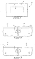
- Fig. 1 shows a top view of a substrate 10 having a memory array region 16 and a peripheral device region 18 surrounding memory array region 16.
- peripheral device region 18 is situated around a periphery of substrate 10, the term “peripheral device” refers primarily to the function of such a device rather than merely to its location.
- the "memory array” portion of a memory device containing memory cells is located centrally on the substrate, such as substrate 10, supporting the memory device.
- “Peripheral devices” including memory cell addressing circuitry and memory cell read circuitry, among other devices, are then located in the periphery around the central memory array.
- alternate positioning of the memory array region and the peripheral device region is conceivable and encompassed by the aspects of the invention described herein.
- the carbonated portions of the semiconductive substrate that contain SiC included in at least some of the individual memory cells may be incorporated into a wide variety of designs for memory devices.
- at least one component of each of the individual memory cells in the array includes one of the carbonated portions.
- none of the peripheral devices include one of the carbonated portions.
- the carbonated portions may be conductively doped.
- the semiconductive substrate may also have a variety of configurations and compositions.
- the semiconductive substrate may include monocystalline silicon.
- the semiconductive substrate may include expitaxial silicon.
- the semiconductive substrate may be part of a bulk silicon wafer or may be part of a semiconductor-on-insulator (SOI) configuration.
- SiC may be incorporated into any semiconductive substrate in conventional memory devices provided at least one of the advantages described herein may be achieved.
- Recent conventional advancements in SiC epitaxial growth present a promising methodology for incorporating SiC into semiconductive substrates. Ion implanting and/or gas diffusing of carbon into a semiconductive substrate, as well as other known methods, present alternatives for incorporating SiC into semiconductive substrates.
- Tetraethyl silane (TES); Si(C 2 H 5 ) 4 ) constitutes one suitable precursor for SiC epitaxial growth.
- TES is liquid at room temperature and easily integrated into a conventional complementary metal-oxide-semiconductor (CMOS) process flow.
- CMOS complementary metal-oxide-semiconductor
- a carbon concentration of from about 0.2 to about 2.5 atomic % carbon in silicon may be suitable to obtain the advantageous SiC properties.
- Preferably, from about 0.5 to about 1.5 atomic % carbon in silicon is provided.
- a memory device forming method includes providing a semiconductive substrate, forming carbonated portions of the semiconductive substrate that contain SiC, forming an array of memory cells over the substrate, and forming peripheral devices including memory cell addressing circuitry and memory cell read circuitry over the substrate. At least some of the individual memory cells include the carbonated portions. At least some of the peripheral devices do not include the carbonated portions.
- Forming the carbonated portions may include forming a masking layer over a memory array region and peripheral device region of the semiconductive substrate, removing the masking layer from over the memory array region, and forming a SiC layer in contact with the memory array region.
- the method includes not forming the SiC layer in contact with the peripheral device region and removing the masking layer from over the peripheral device region.
- Fig. 2 shows a partial sectional view of substrate 10 from Fig. 1 including memory array region 16 and peripheral device region 18.
- Isolation 12 is formed in substrate 10 and a mask 14 is formed over isolation 12 and peripheral device region 18 with the objective of preventing formation of a SiC layer in contact with peripheral device region 18.
- mask 14 may be formed exclusively over peripheral device region 18 and still provide the objective of preventing formation of a SiC layer in contact with peripheral device region 18.
- Silicon nitride constitutes one possibility for a suitable mask 14.
- a SiC layer 8 such as shown in Fig. 3 may be formed in contact with memory array region 16, but not in contact with peripheral device region 18. Selective contact of SiC layer 8 with the respective regions may be accomplished either by selective growth and/or deposition of SiC layer 8 on memory array region 16 or non-selective formation of SiC layer 8 over substrate 10 with mask 14 separating SiC layer 8 from contact with peripheral device region 18.
- SiC layer 8 is shown in Fig. 3 as added material upon memory array region 16. However, SiC layer 8 may instead be formed within substrate 10, for example, by ion implanting and/or gas diffusing carbon. In such case, the elevational level of substrate 10 might not increase as it does in Fig. 3 when the added material of SiC layer 8 increases the original elevational level of substrate 10. Removing mask 14 along with any portion of SiC layer 8 from over isolation 12 and peripheral device region 18 provides the construction shown in Fig. 3 .
- forming the carbonated portions may include forming a SiC layer in contact with a memory array region and a peripheral device region of the semiconductive substrate, removing the SiC layer from over the peripheral device region, and leaving the SiC layer on at least a portion of the memory array region.
- Fig. 4 shows a partial sectional view of substrate 10 in Fig. 1 with SiC layer 8 formed over memory array region 16 as well as peripheral device region 18.
- SiC layer 8 is not shown formed over isolation 12, however, it may be formed thereon depending upon the particular method selected for forming SIC layer 8. Removal of SiC layer 8 from over peripheral device region 18 produces the construction shown in Fig. 3 .
- alternative methods may be used to incorporate SiC into such devices.
- the individual memory cells may contain a planar SiC layer in the semiconductive substrate.
- the individual memory cells may contain a transistor that includes the SiC layer in a first source/drain, a second source/drain, and a channel between the first and second sources/drains.
- Fig. 5 shows a partial, sectional view of selected components of a transistor 20 that may be included in an array of memory cells.
- Transistor 20 includes a SiC layer 22 as a part of substrate 10, a source/drain region 28, and a source/drain region 30 with a channel 29 between the source/drain regions 28, 30.
- a gate dielectric 24 is formed over channel 29 and a gate 26 is formed over gate dielectric 24.
- SiC layer 22 of substrate 10 is included in source/drain region 28, source/drain region 30, and channel 29.
- Transistor 20 also includes a storage node junction 32 formed within source/drain region 28 and a digit node junction 34 formed within source/drain region 30.
- storage/digit node junctions 32 and 34 include SiC layer 22 of source/drain regions 28 and 30.
- a random access memory device in another aspect of the invention, includes a silicon substrate, an array of memory cells over the substrate, and peripheral devices including memory cell addressing circuitry and memory cell read circuitry over the substrate.
- Each of the individual memory cells includes a conductively doped, planar SiC layer in the semiconductive substrate and includes a transistor that contains the SiC layer in a first source/drain, a second source/drain, and a channel between the first and second sources/drains. None of the peripheral devices include any SiC layer in the semiconductive substrate.
- a transistor in further aspect of the invention, includes a semiconductive substrate, a first source/drain, a second source/drain, a channel including a carbonated portion of the semiconductive substrate that contains SiC between the first and second sources/drains and a gate operationally associated with opposing sides of the channel.
- SiC is uniquely provided within the channel of a transistor having a gate operationally associated with opposing sides of the channel in comparison to a gate operationally associated with a single side of the channel.
- the SiC imparts special advantages to such constructions in comparison to transistors with gates on a single side of the channel.
- the transistor of the present aspect of the invention many include a vertical transistor with the channel elevationally above the first source/drain and the second source/drain elevationally above the channel.
- the transistor may include a lateral transistor with some portion of each of the first source/drain, the second source/drain, the gate, and a current path through the channel sharing one common elevational level.
- the transistor may further include a gate dielectric between the gate and the channel.
- the SiC of the channel may be located within a channel periphery proximate an interface with the gate dielectric and not be located within a channel core at least partly surrounded by the SiC.
- the channel core may extend from the first source/drain to the second source/drain.
- the SiC may have a thickness of from about 50 to about 100 Angstroms.
- the transistor may be included in a memory device, for example, a memory device with peripheral devices such as described above that do not include any carbonated portions of the semiconductive substrate.
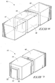
- Figs. 6 and 7 show perspective views of a 3-D transistor that might be referred to by those of ordinary skill as a "FinFET" characterized by a fin-shaped channel.
- 3-D transistor 40 includes a source 42, a drain 46 and a channel 48 extending from source 42 to drain 46.
- a gate 44 over channel 48 can be seen as operationally associated with opposing sides of channel 48.
- Figs. 6 and 7 show only selected components of a 3-D transistor for illustration purposes and intentionally leave out other components, such as the underlying semiconductive substrate, insulation layers, diffusion regions, etc. Also, Figs.
- 3-D transistor 40 may be formed on a semiconductive substrate such that it comprises a lateral transistor and, upon operation of 3-D transistor 40, a current path may be generated through channel 48. Some portion of each of source 42, drain 46, gate 44, and a current path through channel 48 may share one common elevational level.
- Fig. 7 shows the 3-D transistor 40 of Fig. 6 with source 42 removed to reveal details of underlying constructions.
- 3-D transistor 40 includes a gate dielectric 52 between gate 44 and channel 48.
- SiC material 50 is provided within a channel periphery proximate an interface with gate dielectric 52, but is not located within a channel core at least partly surrounded by SiC material 50.
- the channel core extends from source 42 to drain 46.
- One difficulty associated with incorporating SiC into a silicon substrate is that the potential stress and incompatibility at the interface between SiC and Si can produce defects and, hence, leakage currents. Such leakage becomes especially significant when the defects, if any, are in source/drain depletion regions.
- the source/drain depletion regions may be located about the interface of channel 48 with source 42 and with drain 46. With source 42 removed in Fig. 7 , the portion of channel 48 wherein the source depletion region may form is clearly shown. As further known to those of ordinary skill, one part of the source depletion region may extend from the channel 48/source 42 interface into channel 48 to a distance determined by any applied bias.
- Another part of the source depletion region may extend from the channel 48/source 42 interface into source 42 to a distance also determined by any applied bias.
- the depletion regions extend from about 100 to about 800 Angstroms into channel 48 and source 42 for a total depth of from about 200 to about 1600 Angstroms.
- the depletion regions may be far enough away from most defects, if any, at the interface between peripheral SiC material 50 and the channel core of channel 48 not containing SiC so that any defects produced may be of less significance.
- a small part of the peripheral SiC material 50 at either end of channel 48 near source 42 or drain 46 may be within depletion regions.
- the bulk of peripheral SiC material 50 extending along the length of channel 48 between source 42 and drain 46 is advantageously not within depletion regions. Accordingly, the advantages of a SiC-containing channel may still be provided by the configuration shown in Figs. 6 and 7 even in the circumstance when incorporating SiC produces defects at the SiC/Si interface.
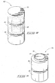
- Figs. 8 and 9 show perspective views of a 3-D transistor 60 oriented vertically instead of laterally.
- Figs. 8 and 9 include only selected components of a typical 3-D transistor for the purposes of illustration as discussed above with regard to 3-D transistor 40.
- the overall configuration of 3-D transistor 60 need not be cylindrical as shown in Figs. 8 and 9 .
- selected components, such as sources/drains and channels may be integral components defined within an underlying semiconductive substrate instead of discrete components as shown.
- 3-D transistor 60 includes a channel 68 elevationally above a drain 66 and a source 62 elevationally above channel 68.
- a gate 64 is operationally associated with opposing sides of channel 68.
- Source 62 is removed in Fig. 9 to reveal the specific construction of channel 68.
- a gate dielectric 72 is provided between gate 64 and channel 68.
- a SiC material 70 is located within a periphery of channel 68 proximate an interface between gate dielectric 72 and channel 68.
- SiC material 70 is not located within a core of channel 68 at least partly surrounded by SiC material 70.
- the channel core extends from source 62 to drain 66.
- the bulk of SiC material 70 is not with a source/drain depletion region.
- the 3-D transistors 40 and 60 of Figs. 6-9 may be produced and/or modified in accordance with any conventional method known for such purpose, except that SiC may be included in the channel of such devices in keeping with the methods described herein. Other than the indicated changes, little if any modification of conventional fabrication methods is expected to accommodate incorporation of SiC.
- a transistor in another aspect of the invention, includes a semiconductive substrate, a first source/drain, a second source/drain, and a gate recessed into the semiconductive substrate between the first and second sources/drains.
- a channel including a carbonated portion of the semiconductive substrate that contains SiC is operationally associated with opposing sides of the gate.
- a gate dielectric may be between the gate and the channel with the SiC of the channel being located within a channel periphery proximate an interface with the gate dielectric.
- the SiC may have a thickness of from about 50 to about 100 Angstroms.
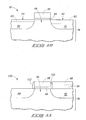
- Transistor 120 includes a SiC layer 130 as a part of a semiconductor substrate 122 and source/drain regions 128 formed within substrate 122.
- a gate dielectric 124 is formed over SiC layer 130 and a gate 126 is formed over gate dielectric 124.
- Gate 126 is referred to as a "recessed gate” since it is located within a recess formed in substrate 122.
- a transistor channel extends between source/drain regions 128 through substrate 122 and includes SiC layer 130.
- SiC layer 130 is also included in source/drain regions 128.
- Transistor 120 with recessed gate 126 represents one example of a structure having a SiC-containing channel operationally associated with opposing sides of a gate.
- a recessed gate device provides a longer gate length for a given feature area.
- a typical planar gate within the same feature area may have a much shorter gate length.
- transistors are often formed with the gate dielectric on a monocrystalline silicon surface exhibiting a ⁇ 100> crystallographic orientation.
- forming the gate dielectric on the ⁇ 100> silicon reduces the interface charge density of the transistor.
- the recess walls may be ⁇ 110> and other orientations depending upon their shape. Accordingly, increased interface charge density may result for a recessed gate device.
- a SiC-containing channel according to the present aspect of the invention may advantageously mitigate the otherwise increased interface charge density because of the SiC material properties described herein.
- a memory cell in a further aspect of the invention, includes a semiconductive substrate, a first transistor source/drain region in the semiconductive substrate, a second transistor source/drain region in the semiconductive substrate, and a transistor channel that does not contain SiC between the first and second source/drain regions.
- a storage node junction is on the first source/drain region and a digit node junction is on the second source/drain region.
- the storage node junction and/or digit node junction include a carbonated portion of the semiconductive substrate that contains SiC. By way of example, if the storage node junction contains SiC, then the SiC has a thickness of from about 200 to about 500 Angstroms.
- the SiC has thickness of from about 50 to about 150 Angstroms.
- the storage and/or digit node junction containing SiC may be on epitaxial silicon of the respective source/drain region.
- the epitaxial silicon may be elevationally above the channel, as in a raised source/drain configuration or other configuration.
- Transistor 80 includes a semiconductive substrate 78, a source/drain region 88 formed within substrate 78, a source/drain region 90 formed within substrate 78, and a transistor channel 89 that does not contain SiC between source/drain regions 88 and 90.
- a storage node junction 94 is on source/drain region 90 and a digit node junction 94 is on source/drain region 88.
- storage node junction 92 includes a SiC layer 82 also within source/drain region 90.
- Digit node junction 94 contains a SiC layer 83 within source/drain region 88.
- the SiC of storage node junction 92 has a greater thickness than the SiC of digit node junction 94.
- Such thickness differences accommodate the general preference for a deeper junction at a storage node in comparison to a digit node.
- a gate dielectric 84 is formed over channel 89 and a gate 86 is formed over gate dielectric 84.
- Transistor 100 includes a raised source/drain 96 that includes a storage/digit node junction 98 therein containing SiC.
- Spacers 102 separate raised source/drain 96 from gate 86.
- Certain conventional configurations for transistors provide a raised source/drain through epitaxial growth of silicon to an elevational level above the channel. Given recent advancements in epitaxial growth techniques of SiC, such epitaxial growth can be combined with epitaxial growth of silicon for a raised source/drain. Process conditions of the growth process may be changed once a desired height for epitaxial silicon is reached such that additional growth provides SiC in the raised source/drain.
- SiC-containing storage/digit node junctions may be included in memory devices with an array of memory cells including carbonated portions of a semiconductive substrate and peripheral devices that do not include any carbonated portions of the semiconductive substrate.
- Possible disadvantages of providing SiC in node junctions includes increased defect density, higher leakage current if defects are not controlled, and some added processing complexity resulting from integrating the SiC.
- possible advantages include reduced junction leakage if defects are controlled and/or their location optimized and shallower junction depths due to less dopant diffusion in the presence of carbon in the SiC. Shallow junction depths are a highly desirable improvement in source/drain regions to control sub-threshold leakage.
- DI BL drain-induced barrier lowering
- SiC-containing channels can reduce DIBL by lessening the dependence of the source injection barrier on drain bias. Even at high drain bias, the source injection barrier is not lowered as significantly compared to a channel lacking the SiC.
- Reducing leakage current may provide a variety of benefits, one of which includes allowing threshold voltage (V t ) and gate-source voltage (V gs ) to be lowered for low-power applications, including DRAM.
- V t threshold voltage
- V gs gate-source voltage
- DRAM dynamic random access memory
- Fig. 13 illustrates generally, by way of example, but not by way of limitation, an embodiment of a computer system 400 according to an aspect of the present invention.
- Computer system 400 includes a monitor 401 or other communication output device, a keyboard 402 or other communication input device, and a motherboard 404.
- Motherboard 404 can carry a microprocessor 406 or other data processing unit, and at least one memory device 408.
- Memory device 408 can comprise various aspects of the invention described above.
- Memory device 408 can comprise an array of memory cells, and such array can be coupled with addressing circuitry for accessing individual memory cells in the array. Further, the memory cell array can be coupled to a read circuit for reading data from the memory cells.
- the addressing and read circuitry can be utilized for conveying information between memory device 408 and processor 406.
- Such is illustrated in the block diagram of the motherboard 404 shown in Fig. 14 . In such block diagram, the addressing circuitry is illustrated as 410 and the read circuitry is illustrated as 412.
- memory device 408 can correspond to a memory module.
- SIMMs single in-line memory modules
- DIMMs dual in-line memory modules
- the memory device can be incorporated into any of a variety of designs that provide different methods of reading from and writing to memory cells of the device.
- One such method is the page mode operation.
- Page mode operations in a DRAM are defined by the method of accessing a row of a memory cell arrays and randomly accessing different columns of the array. Data stored at the row and column intersection can be read and output while that column is accessed.
- An alternative type of device is the extended data output (EDO) memory that allows data stored at a memory array address to be available as output after the addressed column has been closed. This memory can increase some communication speeds by allowing shorter access signals without reducing the time in which memory output data is available on a memory bus.
- EDO extended data output
- Other alternative types of devices include SDRAM, DDR SDRAM, SLDRAM, VRAM and Direct RDRAM, as well as others such as SRAM or Flash memories.
- Fig. 15 illustrates a simplified block diagram of a high-level organization of various embodiments of an exemplary electronic system 700 of the present invention.
- System 700 can correspond to, for example, a computer system, a process control system, or any other system that employs a processor and associated memory.
- Electronic system 700 has functional elements, including a processor or arithmetic/logic unit (ALU) 702, a control unit 704, a memory device unit 706 and an input/output (I/O) device 708.
- ALU arithmetic/logic unit
- control unit 704 controls the memory device unit 706
- I/O input/output
- electronic system 700 will have a native set of instructions that specify operations to be performed on data by the processor 702 and other interactions between the processor 702, the memory device unit 706 and the I/O devices 708.
- the control unit 704 coordinates all operations of the processor 702, the memory device 706 and the I/O devices 708 by continuously cycling through a set of operations that cause instructions to be fetched from the memory device 706 and executed.
- the memory device 706 includes, but is not limited to, random access memory (RAM) devices, read-only memory (ROM) devices, and peripheral devices such as a floppy disk drive and a compact disk CD-ROM drive.
- RAM random access memory
- ROM read-only memory
- peripheral devices such as a floppy disk drive and a compact disk CD-ROM drive.
- Fig. 16 is a simplified block diagram of a high-level organization of various embodiments of an exemplary electronic system 800.
- the system 800 includes a memory device 802 that has an array of memory cells 804, address decoder 806, row access circuitry 808, column access circuitry 810, read/write control circuitry 812 for controlling operations, and input/output circuitry 814.
- the memory device 802 further includes power circuitry 816, and sensors 820, such as current sensors for determining whether a memory cell is in a low-threshold conducting state or in a high-threshold nonconducting state.
- the illustrated power circuitry 816 includes power supply circuitry 880, circuitry 882 for providing a reference voltage, circuitry 884 for providing the first wordline with pulses, circuitry 886 for providing the second wordline with pulses, and circuitry 888 for providing the bitline with pulses.
- the system 800 also includes a processor 822, or memory controller for memory accessing.
- the memory device 802 receives control signals 824 from the processor 822 over wiring or metallization lines.
- the memory device 802 is used to store data that is accessed via I/O lines. It will be appreciated by those skilled in the art that additional circuitry and control signals can be provided, and that the memory device 802 has been simplified to help focus on the invention.
- At least one of the processor 822 or memory device 802 can include a capacitor construction in a memory device of the type described previously herein.
- Applications for memory cells can include electronic systems for use in memory modules, device drivers, power modules, communication modems, processor modules, and application-specific modules, and may include multilayer, multichip modules.
- Such circuitry can further be a subcomponent of a variety of electronic systems, such as a clock, a television, a cell phone, a personal computer, an automobile, an industrial control system, an aircraft, and others.
Landscapes
- Engineering & Computer Science (AREA)
- Manufacturing & Machinery (AREA)
- Semiconductor Memories (AREA)
- Non-Volatile Memory (AREA)
- Insulated Gate Type Field-Effect Transistor (AREA)
- Metal-Oxide And Bipolar Metal-Oxide Semiconductor Integrated Circuits (AREA)
Applications Claiming Priority (2)
| Application Number | Priority Date | Filing Date | Title |
|---|---|---|---|
| US10/902,297 US7598134B2 (en) | 2004-07-28 | 2004-07-28 | Memory device forming methods |
| PCT/US2005/026365 WO2006012626A2 (en) | 2004-07-28 | 2005-07-25 | Memory devices, transistors, memory cells, and methods of making same |
Publications (2)
| Publication Number | Publication Date |
|---|---|
| EP1779425A2 EP1779425A2 (en) | 2007-05-02 |
| EP1779425B1 true EP1779425B1 (en) | 2012-10-03 |
Family
ID=35500865
Family Applications (1)
| Application Number | Title | Priority Date | Filing Date |
|---|---|---|---|
| EP05803899A Expired - Lifetime EP1779425B1 (en) | 2004-07-28 | 2005-07-25 | Memory devices, transistors, memory cells, and methods of making same |
Country Status (7)
| Country | Link |
|---|---|
| US (5) | US7598134B2 (enExample) |
| EP (1) | EP1779425B1 (enExample) |
| JP (1) | JP5207029B2 (enExample) |
| KR (1) | KR100853900B1 (enExample) |
| CN (1) | CN101288166B (enExample) |
| TW (1) | TWI303489B (enExample) |
| WO (1) | WO2006012626A2 (enExample) |
Families Citing this family (25)
| Publication number | Priority date | Publication date | Assignee | Title |
|---|---|---|---|---|
| US7598134B2 (en) | 2004-07-28 | 2009-10-06 | Micron Technology, Inc. | Memory device forming methods |
| US20060194400A1 (en) * | 2005-01-21 | 2006-08-31 | Cooper James A | Method for fabricating a semiconductor device |
| US7465650B2 (en) * | 2005-04-14 | 2008-12-16 | Micron Technology, Inc. | Methods of forming polysilicon-comprising plugs and methods of forming FLASH memory circuitry |
| US7371645B2 (en) * | 2005-12-30 | 2008-05-13 | Infineon Technologies Ag | Method of manufacturing a field effect transistor device with recessed channel and corner gate device |
| US20080283910A1 (en) * | 2007-05-15 | 2008-11-20 | Qimonda Ag | Integrated circuit and method of forming an integrated circuit |
| US7608495B1 (en) * | 2008-09-19 | 2009-10-27 | Micron Technology, Inc. | Transistor forming methods |
| US8816391B2 (en) * | 2009-04-01 | 2014-08-26 | Taiwan Semiconductor Manufacturing Company, Ltd. | Source/drain engineering of devices with high-mobility channels |
| CN101853882B (zh) | 2009-04-01 | 2016-03-23 | 台湾积体电路制造股份有限公司 | 具有改进的开关电流比的高迁移率多面栅晶体管 |
| US8455860B2 (en) | 2009-04-30 | 2013-06-04 | Taiwan Semiconductor Manufacturing Company, Ltd. | Reducing source/drain resistance of III-V based transistors |
| US9768305B2 (en) * | 2009-05-29 | 2017-09-19 | Taiwan Semiconductor Manufacturing Company, Ltd. | Gradient ternary or quaternary multiple-gate transistor |
| JP4530098B1 (ja) | 2009-05-29 | 2010-08-25 | 日本ユニサンティスエレクトロニクス株式会社 | 半導体装置 |
| US8617976B2 (en) * | 2009-06-01 | 2013-12-31 | Taiwan Semiconductor Manufacturing Company, Ltd. | Source/drain re-growth for manufacturing III-V based transistors |
| US8207038B2 (en) * | 2010-05-24 | 2012-06-26 | International Business Machines Corporation | Stressed Fin-FET devices with low contact resistance |
| DE102010040064B4 (de) * | 2010-08-31 | 2012-04-05 | Globalfoundries Inc. | Verringerte Schwellwertspannungs-Breitenabhängigkeit in Transistoren, die Metallgateelektrodenstrukturen mit großem ε aufweisen |
| CN102227001B (zh) * | 2011-06-23 | 2013-03-06 | 北京大学 | 一种锗基nmos器件及其制备方法 |
| ES2686313T3 (es) | 2011-08-22 | 2018-10-17 | Glycotope Gmbh | Microorganismos que portan un antígeno tumoral |
| JP6053490B2 (ja) * | 2011-12-23 | 2016-12-27 | 株式会社半導体エネルギー研究所 | 半導体装置の作製方法 |
| US8647938B1 (en) * | 2012-08-09 | 2014-02-11 | GlobalFoundries, Inc. | SRAM integrated circuits with buried saddle-shaped FINFET and methods for their fabrication |
| EP3080148A2 (en) | 2013-12-11 | 2016-10-19 | Glycotope GmbH | Glycosylated glycophorin peptides |
| US9905648B2 (en) | 2014-02-07 | 2018-02-27 | Stmicroelectronics, Inc. | Silicon on insulator device with partially recessed gate |
| CN109427797B (zh) * | 2017-08-24 | 2020-11-27 | 中芯国际集成电路制造(上海)有限公司 | 半导体结构及其形成方法 |
| US10319424B1 (en) | 2018-01-08 | 2019-06-11 | Spin Memory, Inc. | Adjustable current selectors |
| US10192789B1 (en) * | 2018-01-08 | 2019-01-29 | Spin Transfer Technologies | Methods of fabricating dual threshold voltage devices |
| CN114256245A (zh) * | 2021-12-23 | 2022-03-29 | 波平方科技(杭州)有限公司 | 一种高密度静态随机存储器 |
| WO2023212886A1 (en) * | 2022-05-06 | 2023-11-09 | Yangtze Advanced Memory Industrial Innovation Center Co., Ltd | Memory peripheral circuit having recessed channel transistors and method for forming the same |
Citations (2)
| Publication number | Priority date | Publication date | Assignee | Title |
|---|---|---|---|---|
| EP1104028A2 (en) * | 1999-11-23 | 2001-05-30 | Lucent Technologies Inc. | SiC Nmosfet for use as a power switch and a method of manufacturing the same |
| US20030235076A1 (en) * | 2002-06-21 | 2003-12-25 | Micron Technology, Inc. | Multistate NROM having a storage density much greater than 1 Bit per 1F2 |
Family Cites Families (72)
| Publication number | Priority date | Publication date | Assignee | Title |
|---|---|---|---|---|
| JPS63204766A (ja) | 1987-02-20 | 1988-08-24 | Fujitsu Ltd | 半導体装置 |
| US5289030A (en) * | 1991-03-06 | 1994-02-22 | Semiconductor Energy Laboratory Co., Ltd. | Semiconductor device with oxide layer |
| JP3093011B2 (ja) * | 1991-12-04 | 2000-10-03 | ローム株式会社 | 電界効果トランジスタおよびその製造方法、ならびにそのトランジスタを用いた不揮発性記憶素子および不揮発性記憶装置 |
| US5307305A (en) | 1991-12-04 | 1994-04-26 | Rohm Co., Ltd. | Semiconductor device having field effect transistor using ferroelectric film as gate insulation film |
| US5448081A (en) * | 1993-02-22 | 1995-09-05 | Texas Instruments Incorporated | Lateral power MOSFET structure using silicon carbide |
| US5510630A (en) * | 1993-10-18 | 1996-04-23 | Westinghouse Electric Corporation | Non-volatile random access memory cell constructed of silicon carbide |
| US5514604A (en) | 1993-12-08 | 1996-05-07 | General Electric Company | Vertical channel silicon carbide metal-oxide-semiconductor field effect transistor with self-aligned gate for microwave and power applications, and method of making |
| JPH07235672A (ja) * | 1994-02-21 | 1995-09-05 | Mitsubishi Electric Corp | 絶縁ゲート型半導体装置およびその製造方法 |
| JP3745392B2 (ja) * | 1994-05-26 | 2006-02-15 | 株式会社ルネサステクノロジ | 半導体装置 |
| US5672889A (en) * | 1995-03-15 | 1997-09-30 | General Electric Company | Vertical channel silicon carbide metal-oxide-semiconductor field effect transistor with self-aligned gate for microwave and power applications, and method of making |
| JPH0945692A (ja) * | 1995-07-27 | 1997-02-14 | Sharp Corp | 縦型構造トランジスタ及びその製造方法、並びに半導体装置 |
| JP3305197B2 (ja) * | 1995-09-14 | 2002-07-22 | 株式会社東芝 | 半導体装置 |
| US6150671A (en) * | 1996-04-24 | 2000-11-21 | Abb Research Ltd. | Semiconductor device having high channel mobility and a high breakdown voltage for high power applications |
| US5742076A (en) * | 1996-06-05 | 1998-04-21 | North Carolina State University | Silicon carbide switching devices having near ideal breakdown voltage capability and ultralow on-state resistance |
| JP2910722B2 (ja) | 1997-04-02 | 1999-06-23 | 日本電気株式会社 | 半導体装置 |
| US7154153B1 (en) * | 1997-07-29 | 2006-12-26 | Micron Technology, Inc. | Memory device |
| US6011278A (en) * | 1997-10-28 | 2000-01-04 | Philips Electronics North America Corporation | Lateral silicon carbide semiconductor device having a drift region with a varying doping level |
| JPH11163329A (ja) * | 1997-11-27 | 1999-06-18 | Mitsubishi Electric Corp | 半導体装置およびその製造方法 |
| US6127233A (en) * | 1997-12-05 | 2000-10-03 | Texas Instruments Incorporated | Lateral MOSFET having a barrier between the source/drain regions and the channel region |
| WO1999031719A1 (en) * | 1997-12-17 | 1999-06-24 | Matsushita Electric Industrial Co., Ltd. | Semiconductor thin film, method of producing the same, apparatus for producing the same, semiconductor device and method of producing the same |
| KR100292943B1 (ko) * | 1998-03-25 | 2001-09-17 | 윤종용 | 디램장치의제조방법 |
| JPH11297712A (ja) * | 1998-04-10 | 1999-10-29 | Sanyo Electric Co Ltd | 化合物膜の形成方法及び半導体素子の製造方法 |
| EP1128443B1 (en) * | 1998-10-09 | 2009-12-30 | The Kansai Electric Power Co., Inc. | Field-effect semiconductor device and fabrication method thereof |
| JP2000269496A (ja) * | 1999-03-18 | 2000-09-29 | Toshiba Corp | 半導体装置の製造方法 |
| SE9901440A0 (en) * | 1999-04-22 | 2000-10-23 | Ind Mikroelektronik Centrum Ab | A field effect transistor of SiC for high temperature application, use of such a transistor and a method for production thereof |
| US6281064B1 (en) * | 1999-06-04 | 2001-08-28 | International Business Machines Corporation | Method for providing dual work function doping and protective insulating cap |
| JP2001085685A (ja) * | 1999-09-13 | 2001-03-30 | Shindengen Electric Mfg Co Ltd | トランジスタ |
| US6373076B1 (en) | 1999-12-07 | 2002-04-16 | Philips Electronics North America Corporation | Passivated silicon carbide devices with low leakage current and method of fabricating |
| US6355944B1 (en) * | 1999-12-21 | 2002-03-12 | Philips Electronics North America Corporation | Silicon carbide LMOSFET with gate reach-through protection |
| US6323506B1 (en) * | 1999-12-21 | 2001-11-27 | Philips Electronics North America Corporation | Self-aligned silicon carbide LMOSFET |
| US6372618B2 (en) * | 2000-01-06 | 2002-04-16 | Micron Technology, Inc. | Methods of forming semiconductor structures |
| US6888750B2 (en) | 2000-04-28 | 2005-05-03 | Matrix Semiconductor, Inc. | Nonvolatile memory on SOI and compound semiconductor substrates and method of fabrication |
| JP4632107B2 (ja) * | 2000-06-29 | 2011-02-16 | エルピーダメモリ株式会社 | 半導体記憶装置 |
| JP2004507088A (ja) * | 2000-08-17 | 2004-03-04 | コーニンクレッカ フィリップス エレクトロニクス エヌ ヴィ | トレンチゲート半導体装置の製造方法 |
| US6627924B2 (en) * | 2001-04-30 | 2003-09-30 | Ibm Corporation | Memory system capable of operating at high temperatures and method for fabricating the same |
| US6552363B2 (en) * | 2001-09-18 | 2003-04-22 | International Rectifier Corporation | Polysilicon FET built on silicon carbide diode substrate |
| US6492216B1 (en) * | 2002-02-07 | 2002-12-10 | Taiwan Semiconductor Manufacturing Company | Method of forming a transistor with a strained channel |
| US7176483B2 (en) | 2002-08-12 | 2007-02-13 | Acorn Technologies, Inc. | Method for depinning the Fermi level of a semiconductor at an electrical junction and devices incorporating such junctions |
| US7902029B2 (en) | 2002-08-12 | 2011-03-08 | Acorn Technologies, Inc. | Process for fabricating a self-aligned deposited source/drain insulated gate field-effect transistor |
| US6891234B1 (en) | 2004-01-07 | 2005-05-10 | Acorn Technologies, Inc. | Transistor with workfunction-induced charge layer |
| US6833556B2 (en) | 2002-08-12 | 2004-12-21 | Acorn Technologies, Inc. | Insulated gate field effect transistor having passivated schottky barriers to the channel |
| US7382021B2 (en) | 2002-08-12 | 2008-06-03 | Acorn Technologies, Inc. | Insulated gate field-effect transistor having III-VI source/drain layer(s) |
| US7084423B2 (en) | 2002-08-12 | 2006-08-01 | Acorn Technologies, Inc. | Method for depinning the Fermi level of a semiconductor at an electrical junction and devices incorporating such junctions |
| US6909186B2 (en) * | 2003-05-01 | 2005-06-21 | International Business Machines Corporation | High performance FET devices and methods therefor |
| US7045401B2 (en) * | 2003-06-23 | 2006-05-16 | Sharp Laboratories Of America, Inc. | Strained silicon finFET device |
| US8125003B2 (en) | 2003-07-02 | 2012-02-28 | Micron Technology, Inc. | High-performance one-transistor memory cell |
| US7078742B2 (en) * | 2003-07-25 | 2006-07-18 | Taiwan Semiconductor Manufacturing Co., Ltd. | Strained-channel semiconductor structure and method of fabricating the same |
| TWI313060B (en) * | 2003-07-28 | 2009-08-01 | Japan Science & Tech Agency | Feild effect transisitor and fabricating method thereof |
| US20050067630A1 (en) | 2003-09-25 | 2005-03-31 | Zhao Jian H. | Vertical junction field effect power transistor |
| US20050077574A1 (en) * | 2003-10-08 | 2005-04-14 | Chandra Mouli | 1T/0C RAM cell with a wrapped-around gate device structure |
| US7105390B2 (en) * | 2003-12-30 | 2006-09-12 | Intel Corporation | Nonplanar transistors with metal gate electrodes |
| US7372091B2 (en) * | 2004-01-27 | 2008-05-13 | Micron Technology, Inc. | Selective epitaxy vertical integrated circuit components |
| US7154118B2 (en) * | 2004-03-31 | 2006-12-26 | Intel Corporation | Bulk non-planar transistor having strained enhanced mobility and methods of fabrication |
| US7078723B2 (en) * | 2004-04-06 | 2006-07-18 | Taiwan Semiconductor Manufacturing Company, Ltd. | Microelectronic device with depth adjustable sill |
| US20050230763A1 (en) * | 2004-04-15 | 2005-10-20 | Taiwan Semiconductor Manufacturing Co., Ltd. | Method of manufacturing a microelectronic device with electrode perturbing sill |
| US7452778B2 (en) * | 2004-06-10 | 2008-11-18 | Taiwan Semiconductor Manufacturing Company, Ltd. | Semiconductor nano-wire devices and methods of fabrication |
| US7598134B2 (en) * | 2004-07-28 | 2009-10-06 | Micron Technology, Inc. | Memory device forming methods |
| US7259415B1 (en) | 2004-09-02 | 2007-08-21 | Micron Technology, Inc. | Long retention time single transistor vertical memory gain cell |
| US20060068556A1 (en) * | 2004-09-27 | 2006-03-30 | Matsushita Electric Industrial Co., Ltd. | Semiconductor device and method for fabricating the same |
| US7465976B2 (en) | 2005-05-13 | 2008-12-16 | Intel Corporation | Tunneling field effect transistor using angled implants for forming asymmetric source/drain regions |
| KR100755367B1 (ko) * | 2005-06-08 | 2007-09-04 | 삼성전자주식회사 | 실린더형 게이트를 갖는 나노-라인 반도체 소자 및 그제조방법 |
| KR100724565B1 (ko) * | 2005-07-25 | 2007-06-04 | 삼성전자주식회사 | 코너보호패턴을 갖는 공유콘택구조, 반도체소자, 및 그제조방법들 |
| US20070077739A1 (en) * | 2005-09-30 | 2007-04-05 | Weber Cory E | Carbon controlled fixed charge process |
| JP4592580B2 (ja) | 2005-12-19 | 2010-12-01 | 株式会社東芝 | 不揮発性半導体記憶装置 |
| US7439594B2 (en) | 2006-03-16 | 2008-10-21 | Micron Technology, Inc. | Stacked non-volatile memory with silicon carbide-based amorphous silicon thin film transistors |
| US7843016B2 (en) | 2007-07-16 | 2010-11-30 | International Business Machines Corporation | Asymmetric field effect transistor structure and method |
| US7915670B2 (en) * | 2007-07-16 | 2011-03-29 | International Business Machines Corporation | Asymmetric field effect transistor structure and method |
| US7741658B2 (en) * | 2007-08-21 | 2010-06-22 | International Business Machines Corporation | Self-aligned super stressed PFET |
| JP4798119B2 (ja) * | 2007-11-06 | 2011-10-19 | 株式会社デンソー | 炭化珪素半導体装置およびその製造方法 |
| JP5652939B2 (ja) * | 2010-07-07 | 2015-01-14 | ルネサスエレクトロニクス株式会社 | 半導体装置及び半導体装置の製造方法 |
| US8633096B2 (en) * | 2010-11-11 | 2014-01-21 | International Business Machines Corporation | Creating anisotropically diffused junctions in field effect transistor devices |
| US8513081B2 (en) * | 2011-10-13 | 2013-08-20 | International Business Machines Corporation | Carbon implant for workfunction adjustment in replacement gate transistor |
-
2004
- 2004-07-28 US US10/902,297 patent/US7598134B2/en active Active
-
2005
- 2005-07-25 KR KR1020077001855A patent/KR100853900B1/ko not_active Expired - Lifetime
- 2005-07-25 EP EP05803899A patent/EP1779425B1/en not_active Expired - Lifetime
- 2005-07-25 CN CN200580025205.4A patent/CN101288166B/zh not_active Expired - Lifetime
- 2005-07-25 WO PCT/US2005/026365 patent/WO2006012626A2/en not_active Ceased
- 2005-07-25 JP JP2007523700A patent/JP5207029B2/ja not_active Expired - Lifetime
- 2005-07-27 TW TW094125354A patent/TWI303489B/zh not_active IP Right Cessation
-
2006
- 2006-04-19 US US11/408,874 patent/US8080837B2/en active Active
-
2011
- 2011-11-22 US US13/301,916 patent/US8470666B2/en not_active Expired - Lifetime
- 2011-11-22 US US13/301,921 patent/US8415722B2/en not_active Expired - Lifetime
-
2013
- 2013-05-24 US US13/901,719 patent/US8703566B2/en not_active Expired - Lifetime
Patent Citations (2)
| Publication number | Priority date | Publication date | Assignee | Title |
|---|---|---|---|---|
| EP1104028A2 (en) * | 1999-11-23 | 2001-05-30 | Lucent Technologies Inc. | SiC Nmosfet for use as a power switch and a method of manufacturing the same |
| US20030235076A1 (en) * | 2002-06-21 | 2003-12-25 | Micron Technology, Inc. | Multistate NROM having a storage density much greater than 1 Bit per 1F2 |
Also Published As
| Publication number | Publication date |
|---|---|
| US20060197137A1 (en) | 2006-09-07 |
| US20130248885A1 (en) | 2013-09-26 |
| US20060022239A1 (en) | 2006-02-02 |
| US8470666B2 (en) | 2013-06-25 |
| EP1779425A2 (en) | 2007-05-02 |
| US8080837B2 (en) | 2011-12-20 |
| KR20070029820A (ko) | 2007-03-14 |
| US20120064685A1 (en) | 2012-03-15 |
| TW200629579A (en) | 2006-08-16 |
| US7598134B2 (en) | 2009-10-06 |
| US8415722B2 (en) | 2013-04-09 |
| WO2006012626A3 (en) | 2008-04-17 |
| WO2006012626A2 (en) | 2006-02-02 |
| JP5207029B2 (ja) | 2013-06-12 |
| US8703566B2 (en) | 2014-04-22 |
| KR100853900B1 (ko) | 2008-08-25 |
| CN101288166A (zh) | 2008-10-15 |
| CN101288166B (zh) | 2013-06-26 |
| JP2008508725A (ja) | 2008-03-21 |
| TWI303489B (en) | 2008-11-21 |
| US20120061685A1 (en) | 2012-03-15 |
Similar Documents
| Publication | Publication Date | Title |
|---|---|---|
| US8703566B2 (en) | Transistors comprising a SiC-containing channel | |
| US7569876B2 (en) | DRAM arrays, vertical transistor structures, and methods of forming transistor structures and DRAM arrays | |
| US6881627B2 (en) | Flash memory with ultra thin vertical body transistors | |
| US8803229B2 (en) | Nanowire transistor with surrounding gate | |
| US7224020B2 (en) | Integrated circuit device having non-linear active area pillars | |
| EP2002468B1 (en) | Nanowire transistor with surrounding gate | |
| US7687358B2 (en) | Methods of forming a gated device | |
| JP2008508725A5 (enExample) | ||
| KR20080114806A (ko) | 실리콘 카바이드 기반의 비정질 실리콘 박막 트랜지스터를 구비한 적층형 비휘발성 메모리 및 그 제조 방법 | |
| CN101669200A (zh) | 具有垂直存取装置的存储器 | |
| EP1826819A2 (en) | Semiconductor memory device and manufacturing method thereof | |
| WO2007018967A2 (en) | Methods of forming memory circuitry with different insulative sidewall spacers | |
| CN102473680A (zh) | 存储器单元及形成存储器单元的方法 |
Legal Events
| Date | Code | Title | Description |
|---|---|---|---|
| PUAI | Public reference made under article 153(3) epc to a published international application that has entered the european phase |
Free format text: ORIGINAL CODE: 0009012 |
|
| AK | Designated contracting states |
Kind code of ref document: A2 Designated state(s): AT BE BG CH CY CZ DE DK EE ES FI FR GB GR HU IE IS IT LI LT LU LV MC NL PL PT RO SE SI SK TR |
|
| AX | Request for extension of the european patent |
Extension state: AL BA HR MK YU |
|
| DAX | Request for extension of the european patent (deleted) | ||
| R17D | Deferred search report published (corrected) |
Effective date: 20080417 |
|
| 17P | Request for examination filed |
Effective date: 20070303 |
|
| RIC1 | Information provided on ipc code assigned before grant |
Ipc: H01L 27/06 20060101ALI20080506BHEP Ipc: H01L 27/105 20060101ALI20080506BHEP Ipc: H01L 21/82 20060101AFI20080506BHEP |
|
| 17Q | First examination report despatched |
Effective date: 20090409 |
|
| GRAP | Despatch of communication of intention to grant a patent |
Free format text: ORIGINAL CODE: EPIDOSNIGR1 |
|
| GRAC | Information related to communication of intention to grant a patent modified |
Free format text: ORIGINAL CODE: EPIDOSCIGR1 |
|
| GRAS | Grant fee paid |
Free format text: ORIGINAL CODE: EPIDOSNIGR3 |
|
| GRAA | (expected) grant |
Free format text: ORIGINAL CODE: 0009210 |
|
| AK | Designated contracting states |
Kind code of ref document: B1 Designated state(s): AT BE BG CH CY CZ DE DK EE ES FI FR GB GR HU IE IS IT LI LT LU LV MC NL PL PT RO SE SI SK TR |
|
| REG | Reference to a national code |
Ref country code: GB Ref legal event code: FG4D |
|
| REG | Reference to a national code |
Ref country code: CH Ref legal event code: EP Ref country code: AT Ref legal event code: REF Ref document number: 578331 Country of ref document: AT Kind code of ref document: T Effective date: 20121015 |
|
| REG | Reference to a national code |
Ref country code: IE Ref legal event code: FG4D |
|
| REG | Reference to a national code |
Ref country code: DE Ref legal event code: R096 Ref document number: 602005036428 Country of ref document: DE Effective date: 20121129 |
|
| REG | Reference to a national code |
Ref country code: AT Ref legal event code: MK05 Ref document number: 578331 Country of ref document: AT Kind code of ref document: T Effective date: 20121003 |
|
| PG25 | Lapsed in a contracting state [announced via postgrant information from national office to epo] |
Ref country code: SI Free format text: LAPSE BECAUSE OF FAILURE TO SUBMIT A TRANSLATION OF THE DESCRIPTION OR TO PAY THE FEE WITHIN THE PRESCRIBED TIME-LIMIT Effective date: 20121003 |
|
| REG | Reference to a national code |
Ref country code: NL Ref legal event code: VDEP Effective date: 20121003 |
|
| REG | Reference to a national code |
Ref country code: LT Ref legal event code: MG4D |
|
| PG25 | Lapsed in a contracting state [announced via postgrant information from national office to epo] |
Ref country code: IS Free format text: LAPSE BECAUSE OF FAILURE TO SUBMIT A TRANSLATION OF THE DESCRIPTION OR TO PAY THE FEE WITHIN THE PRESCRIBED TIME-LIMIT Effective date: 20130203 Ref country code: FI Free format text: LAPSE BECAUSE OF FAILURE TO SUBMIT A TRANSLATION OF THE DESCRIPTION OR TO PAY THE FEE WITHIN THE PRESCRIBED TIME-LIMIT Effective date: 20121003 Ref country code: ES Free format text: LAPSE BECAUSE OF FAILURE TO SUBMIT A TRANSLATION OF THE DESCRIPTION OR TO PAY THE FEE WITHIN THE PRESCRIBED TIME-LIMIT Effective date: 20130114 Ref country code: LT Free format text: LAPSE BECAUSE OF FAILURE TO SUBMIT A TRANSLATION OF THE DESCRIPTION OR TO PAY THE FEE WITHIN THE PRESCRIBED TIME-LIMIT Effective date: 20121003 Ref country code: SE Free format text: LAPSE BECAUSE OF FAILURE TO SUBMIT A TRANSLATION OF THE DESCRIPTION OR TO PAY THE FEE WITHIN THE PRESCRIBED TIME-LIMIT Effective date: 20121003 Ref country code: NL Free format text: LAPSE BECAUSE OF FAILURE TO SUBMIT A TRANSLATION OF THE DESCRIPTION OR TO PAY THE FEE WITHIN THE PRESCRIBED TIME-LIMIT Effective date: 20121003 |
|
| PG25 | Lapsed in a contracting state [announced via postgrant information from national office to epo] |
Ref country code: CY Free format text: LAPSE BECAUSE OF FAILURE TO SUBMIT A TRANSLATION OF THE DESCRIPTION OR TO PAY THE FEE WITHIN THE PRESCRIBED TIME-LIMIT Effective date: 20121003 Ref country code: GR Free format text: LAPSE BECAUSE OF FAILURE TO SUBMIT A TRANSLATION OF THE DESCRIPTION OR TO PAY THE FEE WITHIN THE PRESCRIBED TIME-LIMIT Effective date: 20130104 Ref country code: PT Free format text: LAPSE BECAUSE OF FAILURE TO SUBMIT A TRANSLATION OF THE DESCRIPTION OR TO PAY THE FEE WITHIN THE PRESCRIBED TIME-LIMIT Effective date: 20130204 Ref country code: PL Free format text: LAPSE BECAUSE OF FAILURE TO SUBMIT A TRANSLATION OF THE DESCRIPTION OR TO PAY THE FEE WITHIN THE PRESCRIBED TIME-LIMIT Effective date: 20121003 Ref country code: BE Free format text: LAPSE BECAUSE OF FAILURE TO SUBMIT A TRANSLATION OF THE DESCRIPTION OR TO PAY THE FEE WITHIN THE PRESCRIBED TIME-LIMIT Effective date: 20121003 Ref country code: LV Free format text: LAPSE BECAUSE OF FAILURE TO SUBMIT A TRANSLATION OF THE DESCRIPTION OR TO PAY THE FEE WITHIN THE PRESCRIBED TIME-LIMIT Effective date: 20121003 |
|
| PG25 | Lapsed in a contracting state [announced via postgrant information from national office to epo] |
Ref country code: AT Free format text: LAPSE BECAUSE OF FAILURE TO SUBMIT A TRANSLATION OF THE DESCRIPTION OR TO PAY THE FEE WITHIN THE PRESCRIBED TIME-LIMIT Effective date: 20121003 |
|
| PG25 | Lapsed in a contracting state [announced via postgrant information from national office to epo] |
Ref country code: SK Free format text: LAPSE BECAUSE OF FAILURE TO SUBMIT A TRANSLATION OF THE DESCRIPTION OR TO PAY THE FEE WITHIN THE PRESCRIBED TIME-LIMIT Effective date: 20121003 Ref country code: BG Free format text: LAPSE BECAUSE OF FAILURE TO SUBMIT A TRANSLATION OF THE DESCRIPTION OR TO PAY THE FEE WITHIN THE PRESCRIBED TIME-LIMIT Effective date: 20130103 Ref country code: CZ Free format text: LAPSE BECAUSE OF FAILURE TO SUBMIT A TRANSLATION OF THE DESCRIPTION OR TO PAY THE FEE WITHIN THE PRESCRIBED TIME-LIMIT Effective date: 20121003 Ref country code: EE Free format text: LAPSE BECAUSE OF FAILURE TO SUBMIT A TRANSLATION OF THE DESCRIPTION OR TO PAY THE FEE WITHIN THE PRESCRIBED TIME-LIMIT Effective date: 20121003 Ref country code: DK Free format text: LAPSE BECAUSE OF FAILURE TO SUBMIT A TRANSLATION OF THE DESCRIPTION OR TO PAY THE FEE WITHIN THE PRESCRIBED TIME-LIMIT Effective date: 20121003 |
|
| PLBE | No opposition filed within time limit |
Free format text: ORIGINAL CODE: 0009261 |
|
| STAA | Information on the status of an ep patent application or granted ep patent |
Free format text: STATUS: NO OPPOSITION FILED WITHIN TIME LIMIT |
|
| PG25 | Lapsed in a contracting state [announced via postgrant information from national office to epo] |
Ref country code: IT Free format text: LAPSE BECAUSE OF FAILURE TO SUBMIT A TRANSLATION OF THE DESCRIPTION OR TO PAY THE FEE WITHIN THE PRESCRIBED TIME-LIMIT Effective date: 20121003 Ref country code: RO Free format text: LAPSE BECAUSE OF FAILURE TO SUBMIT A TRANSLATION OF THE DESCRIPTION OR TO PAY THE FEE WITHIN THE PRESCRIBED TIME-LIMIT Effective date: 20121003 |
|
| 26N | No opposition filed |
Effective date: 20130704 |
|
| REG | Reference to a national code |
Ref country code: DE Ref legal event code: R097 Ref document number: 602005036428 Country of ref document: DE Effective date: 20130704 |
|
| PG25 | Lapsed in a contracting state [announced via postgrant information from national office to epo] |
Ref country code: MC Free format text: LAPSE BECAUSE OF FAILURE TO SUBMIT A TRANSLATION OF THE DESCRIPTION OR TO PAY THE FEE WITHIN THE PRESCRIBED TIME-LIMIT Effective date: 20121003 |
|
| REG | Reference to a national code |
Ref country code: CH Ref legal event code: PL |
|
| REG | Reference to a national code |
Ref country code: IE Ref legal event code: MM4A |
|
| REG | Reference to a national code |
Ref country code: FR Ref legal event code: ST Effective date: 20140331 |
|
| PG25 | Lapsed in a contracting state [announced via postgrant information from national office to epo] |
Ref country code: LI Free format text: LAPSE BECAUSE OF NON-PAYMENT OF DUE FEES Effective date: 20130731 Ref country code: CH Free format text: LAPSE BECAUSE OF NON-PAYMENT OF DUE FEES Effective date: 20130731 |
|
| PG25 | Lapsed in a contracting state [announced via postgrant information from national office to epo] |
Ref country code: FR Free format text: LAPSE BECAUSE OF NON-PAYMENT OF DUE FEES Effective date: 20130731 |
|
| PG25 | Lapsed in a contracting state [announced via postgrant information from national office to epo] |
Ref country code: IE Free format text: LAPSE BECAUSE OF NON-PAYMENT OF DUE FEES Effective date: 20130725 |
|
| PG25 | Lapsed in a contracting state [announced via postgrant information from national office to epo] |
Ref country code: TR Free format text: LAPSE BECAUSE OF FAILURE TO SUBMIT A TRANSLATION OF THE DESCRIPTION OR TO PAY THE FEE WITHIN THE PRESCRIBED TIME-LIMIT Effective date: 20121003 |
|
| PG25 | Lapsed in a contracting state [announced via postgrant information from national office to epo] |
Ref country code: LU Free format text: LAPSE BECAUSE OF NON-PAYMENT OF DUE FEES Effective date: 20130725 Ref country code: HU Free format text: LAPSE BECAUSE OF FAILURE TO SUBMIT A TRANSLATION OF THE DESCRIPTION OR TO PAY THE FEE WITHIN THE PRESCRIBED TIME-LIMIT; INVALID AB INITIO Effective date: 20050725 |
|
| PGFP | Annual fee paid to national office [announced via postgrant information from national office to epo] |
Ref country code: GB Payment date: 20150722 Year of fee payment: 11 |
|
| GBPC | Gb: european patent ceased through non-payment of renewal fee |
Effective date: 20160725 |
|
| PG25 | Lapsed in a contracting state [announced via postgrant information from national office to epo] |
Ref country code: GB Free format text: LAPSE BECAUSE OF NON-PAYMENT OF DUE FEES Effective date: 20160725 |
|
| PGFP | Annual fee paid to national office [announced via postgrant information from national office to epo] |
Ref country code: DE Payment date: 20240730 Year of fee payment: 20 |
|
| REG | Reference to a national code |
Ref country code: DE Ref legal event code: R079 Ref document number: 602005036428 Country of ref document: DE Free format text: PREVIOUS MAIN CLASS: H01L0021820000 Ipc: H10D0089000000 |
|
| REG | Reference to a national code |
Ref country code: DE Ref legal event code: R071 Ref document number: 602005036428 Country of ref document: DE |