EP1763083A2 - Halbleiteranordnung - Google Patents
Halbleiteranordnung Download PDFInfo
- Publication number
- EP1763083A2 EP1763083A2 EP06019023A EP06019023A EP1763083A2 EP 1763083 A2 EP1763083 A2 EP 1763083A2 EP 06019023 A EP06019023 A EP 06019023A EP 06019023 A EP06019023 A EP 06019023A EP 1763083 A2 EP1763083 A2 EP 1763083A2
- Authority
- EP
- European Patent Office
- Prior art keywords
- diffusion layer
- layer
- region
- type diffusion
- regions
- Prior art date
- Legal status (The legal status is an assumption and is not a legal conclusion. Google has not performed a legal analysis and makes no representation as to the accuracy of the status listed.)
- Granted
Links
- 239000004065 semiconductor Substances 0.000 title claims abstract description 36
- 238000009792 diffusion process Methods 0.000 claims abstract description 168
- 229910052751 metal Inorganic materials 0.000 claims abstract description 32
- 239000002184 metal Substances 0.000 claims abstract description 32
- 239000012535 impurity Substances 0.000 claims description 16
- 230000008878 coupling Effects 0.000 claims description 11
- 238000010168 coupling process Methods 0.000 claims description 11
- 238000005859 coupling reaction Methods 0.000 claims description 11
- 239000010410 layer Substances 0.000 description 212
- 239000000758 substrate Substances 0.000 description 12
- 230000004888 barrier function Effects 0.000 description 7
- 238000002955 isolation Methods 0.000 description 7
- 230000008859 change Effects 0.000 description 6
- 230000005684 electric field Effects 0.000 description 6
- 210000000746 body region Anatomy 0.000 description 4
- 230000006866 deterioration Effects 0.000 description 4
- 238000005516 engineering process Methods 0.000 description 3
- 229910021421 monocrystalline silicon Inorganic materials 0.000 description 3
- CSDREXVUYHZDNP-UHFFFAOYSA-N alumanylidynesilicon Chemical compound [Al].[Si] CSDREXVUYHZDNP-UHFFFAOYSA-N 0.000 description 2
- 230000015572 biosynthetic process Effects 0.000 description 2
- 239000000969 carrier Substances 0.000 description 2
- 239000000463 material Substances 0.000 description 2
- 230000008018 melting Effects 0.000 description 2
- 238000002844 melting Methods 0.000 description 2
- 229910021420 polycrystalline silicon Inorganic materials 0.000 description 2
- 229920005591 polysilicon Polymers 0.000 description 2
- 239000002356 single layer Substances 0.000 description 2
- ZOXJGFHDIHLPTG-UHFFFAOYSA-N Boron Chemical compound [B] ZOXJGFHDIHLPTG-UHFFFAOYSA-N 0.000 description 1
- XPDWGBQVDMORPB-UHFFFAOYSA-N Fluoroform Chemical compound FC(F)F XPDWGBQVDMORPB-UHFFFAOYSA-N 0.000 description 1
- 229910052782 aluminium Inorganic materials 0.000 description 1
- XAGFODPZIPBFFR-UHFFFAOYSA-N aluminium Chemical compound [Al] XAGFODPZIPBFFR-UHFFFAOYSA-N 0.000 description 1
- WPPDFTBPZNZZRP-UHFFFAOYSA-N aluminum copper Chemical compound [Al].[Cu] WPPDFTBPZNZZRP-UHFFFAOYSA-N 0.000 description 1
- -1 aluminum-silicon-copper Chemical compound 0.000 description 1
- 229910052796 boron Inorganic materials 0.000 description 1
- 150000001875 compounds Chemical class 0.000 description 1
- 230000001419 dependent effect Effects 0.000 description 1
- 230000002542 deteriorative effect Effects 0.000 description 1
- 238000001312 dry etching Methods 0.000 description 1
- 230000000694 effects Effects 0.000 description 1
- 239000011521 glass Substances 0.000 description 1
- 230000006872 improvement Effects 0.000 description 1
- 230000003071 parasitic effect Effects 0.000 description 1
- 239000005360 phosphosilicate glass Substances 0.000 description 1
- 238000000206 photolithography Methods 0.000 description 1
- 230000002265 prevention Effects 0.000 description 1
- 230000009467 reduction Effects 0.000 description 1
- WNUPENMBHHEARK-UHFFFAOYSA-N silicon tungsten Chemical compound [Si].[W] WNUPENMBHHEARK-UHFFFAOYSA-N 0.000 description 1
- WFKWXMTUELFFGS-UHFFFAOYSA-N tungsten Chemical compound [W] WFKWXMTUELFFGS-UHFFFAOYSA-N 0.000 description 1
- 229910052721 tungsten Inorganic materials 0.000 description 1
- 239000010937 tungsten Substances 0.000 description 1
Images



Classifications
-
- H—ELECTRICITY
- H10—SEMICONDUCTOR DEVICES; ELECTRIC SOLID-STATE DEVICES NOT OTHERWISE PROVIDED FOR
- H10D—INORGANIC ELECTRIC SEMICONDUCTOR DEVICES
- H10D62/00—Semiconductor bodies, or regions thereof, of devices having potential barriers
- H10D62/10—Shapes, relative sizes or dispositions of the regions of the semiconductor bodies; Shapes of the semiconductor bodies
- H10D62/102—Constructional design considerations for preventing surface leakage or controlling electric field concentration
- H10D62/103—Constructional design considerations for preventing surface leakage or controlling electric field concentration for increasing or controlling the breakdown voltage of reverse-biased devices
- H10D62/105—Constructional design considerations for preventing surface leakage or controlling electric field concentration for increasing or controlling the breakdown voltage of reverse-biased devices by having particular doping profiles, shapes or arrangements of PN junctions; by having supplementary regions, e.g. junction termination extension [JTE]
- H10D62/106—Constructional design considerations for preventing surface leakage or controlling electric field concentration for increasing or controlling the breakdown voltage of reverse-biased devices by having particular doping profiles, shapes or arrangements of PN junctions; by having supplementary regions, e.g. junction termination extension [JTE] having supplementary regions doped oppositely to or in rectifying contact with regions of the semiconductor bodies, e.g. guard rings with PN or Schottky junctions
-
- H—ELECTRICITY
- H10—SEMICONDUCTOR DEVICES; ELECTRIC SOLID-STATE DEVICES NOT OTHERWISE PROVIDED FOR
- H10D—INORGANIC ELECTRIC SEMICONDUCTOR DEVICES
- H10D30/00—Field-effect transistors [FET]
- H10D30/60—Insulated-gate field-effect transistors [IGFET]
- H10D30/64—Double-diffused metal-oxide semiconductor [DMOS] FETs
- H10D30/65—Lateral DMOS [LDMOS] FETs
-
- H—ELECTRICITY
- H10—SEMICONDUCTOR DEVICES; ELECTRIC SOLID-STATE DEVICES NOT OTHERWISE PROVIDED FOR
- H10D—INORGANIC ELECTRIC SEMICONDUCTOR DEVICES
- H10D30/00—Field-effect transistors [FET]
- H10D30/60—Insulated-gate field-effect transistors [IGFET]
- H10D30/64—Double-diffused metal-oxide semiconductor [DMOS] FETs
- H10D30/65—Lateral DMOS [LDMOS] FETs
- H10D30/655—Lateral DMOS [LDMOS] FETs having edge termination structures
-
- H—ELECTRICITY
- H10—SEMICONDUCTOR DEVICES; ELECTRIC SOLID-STATE DEVICES NOT OTHERWISE PROVIDED FOR
- H10D—INORGANIC ELECTRIC SEMICONDUCTOR DEVICES
- H10D62/00—Semiconductor bodies, or regions thereof, of devices having potential barriers
- H10D62/10—Shapes, relative sizes or dispositions of the regions of the semiconductor bodies; Shapes of the semiconductor bodies
- H10D62/124—Shapes, relative sizes or dispositions of the regions of semiconductor bodies or of junctions between the regions
- H10D62/126—Top-view geometrical layouts of the regions or the junctions
- H10D62/127—Top-view geometrical layouts of the regions or the junctions of cellular field-effect devices, e.g. multicellular DMOS transistors or IGBTs
-
- H—ELECTRICITY
- H10—SEMICONDUCTOR DEVICES; ELECTRIC SOLID-STATE DEVICES NOT OTHERWISE PROVIDED FOR
- H10D—INORGANIC ELECTRIC SEMICONDUCTOR DEVICES
- H10D62/00—Semiconductor bodies, or regions thereof, of devices having potential barriers
- H10D62/10—Shapes, relative sizes or dispositions of the regions of the semiconductor bodies; Shapes of the semiconductor bodies
- H10D62/13—Semiconductor regions connected to electrodes carrying current to be rectified, amplified or switched, e.g. source or drain regions
- H10D62/149—Source or drain regions of field-effect devices
- H10D62/151—Source or drain regions of field-effect devices of IGFETs
- H10D62/156—Drain regions of DMOS transistors
- H10D62/157—Impurity concentrations or distributions
-
- H—ELECTRICITY
- H10—SEMICONDUCTOR DEVICES; ELECTRIC SOLID-STATE DEVICES NOT OTHERWISE PROVIDED FOR
- H10D—INORGANIC ELECTRIC SEMICONDUCTOR DEVICES
- H10D62/00—Semiconductor bodies, or regions thereof, of devices having potential barriers
- H10D62/10—Shapes, relative sizes or dispositions of the regions of the semiconductor bodies; Shapes of the semiconductor bodies
- H10D62/17—Semiconductor regions connected to electrodes not carrying current to be rectified, amplified or switched, e.g. channel regions
- H10D62/393—Body regions of DMOS transistors or IGBTs
-
- H—ELECTRICITY
- H10—SEMICONDUCTOR DEVICES; ELECTRIC SOLID-STATE DEVICES NOT OTHERWISE PROVIDED FOR
- H10D—INORGANIC ELECTRIC SEMICONDUCTOR DEVICES
- H10D64/00—Electrodes of devices having potential barriers
- H10D64/111—Field plates
-
- H—ELECTRICITY
- H10—SEMICONDUCTOR DEVICES; ELECTRIC SOLID-STATE DEVICES NOT OTHERWISE PROVIDED FOR
- H10D—INORGANIC ELECTRIC SEMICONDUCTOR DEVICES
- H10D64/00—Electrodes of devices having potential barriers
- H10D64/20—Electrodes characterised by their shapes, relative sizes or dispositions
- H10D64/27—Electrodes not carrying the current to be rectified, amplified, oscillated or switched, e.g. gates
- H10D64/311—Gate electrodes for field-effect devices
- H10D64/411—Gate electrodes for field-effect devices for FETs
- H10D64/511—Gate electrodes for field-effect devices for FETs for IGFETs
- H10D64/514—Gate electrodes for field-effect devices for FETs for IGFETs characterised by the insulating layers
- H10D64/516—Gate electrodes for field-effect devices for FETs for IGFETs characterised by the insulating layers the thicknesses being non-uniform
-
- H—ELECTRICITY
- H10—SEMICONDUCTOR DEVICES; ELECTRIC SOLID-STATE DEVICES NOT OTHERWISE PROVIDED FOR
- H10D—INORGANIC ELECTRIC SEMICONDUCTOR DEVICES
- H10D64/00—Electrodes of devices having potential barriers
- H10D64/60—Electrodes characterised by their materials
- H10D64/66—Electrodes having a conductor capacitively coupled to a semiconductor by an insulator, e.g. MIS electrodes
- H10D64/661—Electrodes having a conductor capacitively coupled to a semiconductor by an insulator, e.g. MIS electrodes the conductor comprising a layer of silicon contacting the insulator, e.g. polysilicon having vertical doping variation
- H10D64/662—Electrodes having a conductor capacitively coupled to a semiconductor by an insulator, e.g. MIS electrodes the conductor comprising a layer of silicon contacting the insulator, e.g. polysilicon having vertical doping variation the conductor further comprising additional layers, e.g. multiple silicon layers having different crystal structures
- H10D64/663—Electrodes having a conductor capacitively coupled to a semiconductor by an insulator, e.g. MIS electrodes the conductor comprising a layer of silicon contacting the insulator, e.g. polysilicon having vertical doping variation the conductor further comprising additional layers, e.g. multiple silicon layers having different crystal structures the additional layers comprising a silicide layer contacting the layer of silicon, e.g. polycide gates
Definitions
- the present invention relates to a semiconductor device of high withstand voltage, which improves withstand voltage characteristics of its inactive region.
- a conventional semiconductor device such as an N channel type MOS transistor, is formed in an elliptical shape.
- the semiconductor device includes an N type drain region disposed in its center region, an N type buffer region disposed circularly surrounding the N type drain region, and an N type drift region disposed circularly surrounding the N type buffer region.
- the semiconductor device also includes a P type well region disposed surrounding the N type drift region, and an N type source region disposed in each of linear regions of the P type well region.
- a conventional semiconductor device such as an N channel type MOS transistor, is formed in an elliptical shape as previously mentioned.
- the semiconductor device includes a P type semiconductor substrate, a semiconductor layer formed on the P type semiconductor substrate, a P type body region formed on the semiconductor layer, and an N type source region and a P type contact region which are formed in the P type body region.
- the semiconductor device also includes a drain region formed on the semiconductor layer, and a field oxide film formed between the drain region and the body region.
- the semiconductor device further includes four P type floating field rings disposed circularly under the field oxide film. This technology is described for instance in Japanese Patent Application Publication No. 2005-93696 , pp. 6 and 7, and Figs. 1 and 2.
- the conventional semiconductor device is formed in the elliptical shape.
- the semiconductor device includes the P type well region in a circular form, which is formed in linear regions and round regions to be used as active regions and inactive regions, respectively.
- the conventional semiconductor device has a problem that it is difficult to achieve desired withstand voltage characteristics, since the inactive regions in particular, with the same structure as that of the linear regions, is prone to convergence of an electric field due to its round shape when the MOS transistor is off.
- the conventional N channel type MOS transistor includes the four P type floating field rings, which are circularly disposed between the drain region and the body region, in order to improve the withstand voltage characteristics of the round region.
- the conventional MOS transistor has a problem that it is difficult to achieve desired current characteristics, since the P type floating field rings form barriers against the flow of free carriers (electrons) between the drain and source regions and thus lead to an increase in the on-state resistance value.
- the conventional semiconductor device includes the field oxide film formed between the drain and source regions, as mentioned above. With this structure, the conventional semiconductor device has a problem that it is difficult to achieve desired current characteristics, since the field oxide film forms a barrier against the flow of free carriers (electrons) between the drain and source regions and thus leads to an increase in the on-state resistance value.
- the invention provides a semiconductor device that includes a semiconductor layer having an active region and an inactive region.
- the active region has a source region, a drain region and a gate electrode formed therein, and the inactive region has neither a source region, a drain region nor a gate electrode.
- the device also includes an insulating layer disposed on the semiconductor layer, a first diffusion layer formed in the inactive region so as to be floating, a second diffusion layer formed in the active and inactive regions so as to be floating, and a metal layer disposed on the insulating film so as to form capacitive coupling with the first and second diffusion layers where the first diffusion layer merges with the second diffusion layer.
- Fig. 1 is a plan view for explaining an N channel type MOS transistor according to the embodiment.
- Fig. 2 is a cross-sectional view taken along the line A-A of Fig. 1, for explaining the N channel type MOS transistor according to the embodiment.
- Fig. 3 is a cross-sectional view taken along the line B-B of Fig. 1, for explaining the N channel type MOS transistor according to the embodiment.
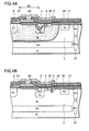
- Fig. 4A is a view for explaining the potential distribution in a reverse state of the N channel type MOS transistor according to the embodiment.
- Fig. 4B is a view for explaining an impact ionization region of the N channel type MOS transistor according to the embodiment.
- Fig. 5A is a view for explaining the potential distribution in a reverse bias state of the N channel type MOS transistor according to the embodiment.
- Fig. 5B is a view for explaining the impact ionization region of the N channel type MOS transistor according to the embodiment.
- the N channel type MOS transistor 1 is formed in an elliptical shape, for example.
- Linear regions L in the elliptical shape include a source region disposed in its center region, and drain regions disposed on both sides of the source region.
- the linear regions L let a current pass between the drain and source regions, i.e., along the x axis.
- the linear regions L are used as active regions which let the current pass.
- round regions R in the elliptical shape are used as inactive regions which do not let the current pass.
- a P type diffusion layer 2 is circularly formed, extending across both the active and inactive regions.
- the P type diffusion layer 2 is disposed in a region shown by the dash-dot line in Fig. 1, and is disposed between the source and drain regions in the active regions.
- P type diffusion layers 3 and 4 respectively shown by the dash-double-dot line and the dotted line in Fig. 1, are formed in order to improve the withstand voltage characteristics in the inactive regions, although the detailed description thereof will be given later with reference to Figs. 4A to 5B.
- the P type diffusion layer 2 in the embodiment corresponds to a "second diffusion layer” of the present invention.
- the P type diffusion layers 3 in the embodiment correspond to "first diffusion layers” of the present invention.
- the P type diffusion layer 4 in the embodiment corresponds to a "third diffusion layer” of the present invention.
- Reference numerals enclosed within parentheses in Fig. 1 correspond to reference numerals given in Figs. 2 and 3.
- a cross-section taken along the line A-A of Fig. 1 shows a cross-section of the active region of the MOS transistor 1.
- the MOS transistor 1 is configured mainly with: the P type diffusion layer 2; a P type single crystal silicon substrate 5; an N type buried diffusion layer 6; an N type epitaxial layer 7; P type diffusion layers 8, 9, 10 and 11 to be used as back gate regions; an N type diffusion layer 12 to be used as the source region; N type diffusion layers 13, 14 and 15 to be used as the drain regions; and a gate electrode 16.
- the P type diffusion layer 2 is formed in the epitaxial layer 7. As mentioned above, the P type diffusion layer 2 is circularly formed as surrounding the P type diffusion layer 8 which is used as the back gate region.
- the P type diffusion layer 2 is formed, for example, under conditions of diffusion where the surface of the P type diffusion layer 2 has an impurity concentration of about 1.0 ⁇ 10 15 to 1.0 ⁇ 10 16 (1/cm 3 ) and a diffusion depth of about 1 to 3 ( ⁇ m).
- the P type diffusion layer 2 is formed as a floating diffusion layer and forms capacitive coupling with metal layers 25 and 26 above the P type diffusion layer 2.
- the P type diffusion layer 2 is designed to have the impurity concentration in consideration of the withstand voltage characteristics and the on-state resistance value, because the on-state resistance value increases when the P type diffusion layer 2 is formed in the active regions.
- the N type epitaxial layer 7 is formed above the P type single crystal silicon substrate 5.
- the N type buried diffusion layer 6 is formed between the substrate 5 and the epitaxial layer 7.
- the substrate 5 and the epitaxial layer 7 in the embodiment correspond to a "semiconductor layer" of the present invention.
- the "semiconductor layer" of the embodiment of the present invention may be formed of the substrate alone or may be formed of the substrate and a plurality of epitaxial layers deposited thereon.
- the substrate may be formed of an N type single crystal silicon substrate or a compound semiconductor substrate.
- the P type diffusion layer 8 is formed in the epitaxial layer 7.
- the P type diffusion layers 9, 10 and 11 are formed in the P type diffusion layer 8 in such a manner that the diffusion layers 9, 10 and 11 are superposed on the diffusion layer 8.
- the P type diffusion layer 9 being superposed on the P type diffusion layer 8 achieves reduction in the resistance value of the back gate region and hence achieves prevention of operation of a parasitic NPN transistor.
- the N type diffusion layer 12 is formed in the P type diffusion layer 9.
- the N type diffusion layer 12 is used as the source region.
- the N type diffusion layer 12 and the P type diffusion layer 11 are connected to source electrodes S and are at the same potential.
- the P type diffusion layers 10 and 11 are disposed as being surrounded by the N type diffusion layer 12, and are used as back gate lead regions.
- the P type diffusion layers 10 and 11 are formed as high-concentration impurity regions, thereby making it possible to reduce contact resistance.
- the N type diffusion layers 13, 14 and 15 are formed in the epitaxial layer 7.
- the N type diffusion layers 13, 14 and 15 are used as the drain regions.
- the N type diffusion layer 13 is circularly disposed, extending across both the active and inactive regions.
- the N type diffusion layers 14 and 15 are disposed in the active regions on both sides of the N type diffusion layer 12 which forms the source region.
- the P type diffusion layers 8 and 9, which are located under the gate electrode 16 and which are located between the N type diffusion layers 12 and 15, are used as channel regions.
- the gate electrode 16 is formed on a top surface of a gate oxide film 17.
- the gate electrode 16 is made of, for example, a polycide film which is a deposited film formed of a polysilicon film and a tungsten silicide (WSi) film.
- the gate electrode 16 is formed with a desired film thickness.
- the gate electrode 16 may be made of a single layer film formed of a polysilicon film, other various single layer films or deposited films, or the like.
- the insulating layer 18 is formed on a top surface of the epitaxial layer 7.
- the insulating layer 18 is made of a BPSG (boron phospho silicate glass) film, an SOG (spin on glass) film, or the like.
- BPSG boron phospho silicate glass
- SOG spin on glass
- photolithography technology is used for, for example, dry etching using CHF 3 +O 2 base gas to form contact holes 19, 20 and 21 in the insulating layer 18.
- Metal layers 22, 23 and 24 are buried in the contact holes 19, 20 and 21, respectively.
- the metal layers 22, 23 and 24 each have a structure formed of, for example, an aluminum-silicon (Al-Si) layer, an aluminum-copper (Al-Cu) layer or an aluminum-silicon-copper (Al-Si-Cu) layer deposited on a barrier metal layer.
- the metal layers 22, 23 and 24 may be each formed of a barrier metal layer and a metal layer in each of the contact holes 19, 20 and 21.
- the metal layer made of a high melting point metal such as tungsten (W) is buried in the barrier metal layer.
- a metal layer composed almost exclusively of aluminum is formed on the metal layer made of the high melting point metal.
- the metal layers 25 and 26 are formed on a top surface of the insulating layer 18 to cover the P type diffusion layer 2.
- the metal layers 25 and 26 are wiring layers, although not shown, connected to the source electrodes S.
- the P type diffusion layer 2 forms capacitive coupling with the metal layers 25 and 26 through the gate oxide film 17, the insulating layer 18, and so on interposed in between. Desired potentials are applied to the P type diffusion layer 2, although the potentials are slightly higher than a source potential.
- the P type diffusion layer 2 is biased in a direction reverse to the N type epitaxial layer 7, thereby improving the withstand voltage characteristics of the MOS transistor 1.
- a cross-section taken along the line B-B of Fig. 1 shows a cross-section of the inactive regions of the MOS transistor 1.
- omitted is the cross-section of the active regions which are the linear regions L in the elliptical shape, and mainly shown is the cross-section of the inactive regions which are the round regions R in the elliptical shape.
- the cross-section shown on the right side of the omitted part corresponds to a lower section along the y axis in Fig. 1.
- the cross-section shown on the left side of the omitted part corresponds to an upper section along the y axis in Fig. 1.
- LOCOS oxide films 27 and 28 are each formed between the P type diffusion layer 8 and the N type diffusion layer 13.
- the LOCOS oxide films 27 and 28 are each formed only in the inactive regions which are the round regions R, and are not formed in the active regions which are the linear regions L.
- respective ends of the gate electrode 16 are disposed on the LOCOS oxide films 27 or 28.
- the LOCOS oxide films 27 and 28 cause the gate electrode 16 to be apart from the surface of the epitaxial layer 7, so that this structure makes it possible to improve the withstand voltage characteristics.
- the LOCOS oxide films 27 and 28 in the embodiment correspond to "field oxide films" of the present invention.
- a metal layer 30 is connected to the gate electrode 16 through a contact hole 29 formed in the insulating layer 18.
- the metal layer 30 extends toward an isolation region 31 to cover the P type diffusion layer 2.
- the P type diffusion layer 2 forms capacitive coupling with the metal layer 30 through the gate oxide film 17, the insulating layer 18, and so on interposed in between.
- metal layer 32 is formed as being located above the P type diffusion layer 2.
- the metal layer 32 is connected to the source electrodes S, and the P type diffusion layer 2 forms capacitive coupling with the metal layer 32 through the gate oxide film 17, the insulating layer 18, and so on interposed in between.
- one of the P type diffusion layers 3 is formed on an end of the LOCOS oxide film 27 and in its vicinity to coincide with the shape of the round regions R, as shown by the dash-double-dot lines in Fig. 1.
- the corresponding P type diffusion layer 3 is formed as a floating diffusion layer in such a manner that a formation region of the P type diffusion layer 2 and a formation region of the P type diffusion layer 3 are superposed on each other.
- the P type diffusion layer 4 is formed to correspond to a region, in a vicinity of the contact hole 29, where a width W1 of the LOCOS oxide film 27 is greater.
- the width W1 of the LOCOS oxide film 27 is greater than a width W2 of the LOCOS oxide film 28.
- the reason is that a flat region is required above the LOCOS oxide film 27 in order to connect the metal layer 30 to the gate electrode 16, as mentioned above.
- the width of the LOCOS oxide film 27 is equal to the width W2 in regions other than the vicinity of the contact hole 29.
- the P type diffusion layers 3 and 4 form capacitive coupling with the metal layer 30 on the top surface of the insulating layer 18, as in the case of the P type diffusion layer 2.
- the P type diffusion layers 3 are formed, for example, under conditions of diffusion where each of the surfaces of the P type diffusion layers 3 has an impurity concentration of about 1.0 ⁇ 10 17 to 1.0 ⁇ 10 18 (1/cm 3 ) and a diffusion depth of about 2 to 4 ( ⁇ m).
- the P type diffusion layer 4 is formed, for example, under conditions of diffusion where the surface of the P type diffusion layer 4 has an impurity concentration of about 1.0 ⁇ 10 16 to 1.0 ⁇ 10 17 (1/cm 3 ) and a diffusion depth of about 5 to 6 ( ⁇ m).
- one of the P type diffusion layers 3 is formed on an end of the LOCOS oxide film 28 and in its vicinity to coincide with the shape of the round regions R.
- the corresponding P type diffusion layer 3 is formed as a floating diffusion layer in such a manner that the P type diffusion layer 2 and the P type diffusion layer 3 are superposed on each other.
- the corresponding P type diffusion layer 3 forms capacitive coupling with the metal layer 32 on the top surface of the insulating layer 18, as in the case of the P type diffusion layer 2.
- each of the inactive regions has a structure which is prone to convergence of an electric field due to its round shape.
- the P type diffusion layers 2, 3 and 4 are disposed in one of the inactive regions, so that it is possible to further improve the withstand voltage characteristics in the corresponding inactive region, as compared to the active regions.
- the P type diffusion layers 3 and 4 are disposed only in the inactive regions and are not disposed in the active regions.
- the active regions are the linear regions whose structure is less prone to convergence of an electric field than the inactive regions.
- the active regions have the structure in which only the P type diffusion layer 2 is disposed, so that the withstand voltage characteristics of the MOS transistor 1 are determined by the withstand voltage characteristics of the active regions.
- the active regions do not have to have P type diffusion layers more than necessary, thus making it possible to prevent an increase in the on-state resistance value of the MOS transistor 1 due to excess P type diffusion layers becoming barriers. This structure also makes it possible to prevent an increase in device size.
- Fig. 4A there is shown a region, near the LOCOS oxide film 27 in the vicinity of the contact hole 29, where the P type diffusion layer 4 is formed.
- the bold solid lines show end regions of a depletion layer
- the dotted lines show equipotential lines
- the dash-dot line shows an equipotential line at 359 V.
- the P type diffusion layers 2, 3 and 4 are formed as the floating diffusion layers, there is a region to which a potential slightly higher than a gate potential is applied.
- the region where the P type diffusion layers 2, 3 and 4 are superposed on one another is a high-concentration impurity region, and an undepleted region is present as shown by the solid line. The reason is that the undepleted P type diffusion layers 2, 3 and 4 form capacitive coupling with the metal layer 30, as mentioned above.
- the P type diffusion layer 4 is diffused to the same depth as the depth of the P type diffusion layer 8.
- a depletion layer which extends from a boundary between the P type diffusion layer 4 and the epitaxial layer 7, extends over a wide region in a horizontal direction, as in the case of a depletion layer which extends from a boundary between the P type diffusion layer 8 and the epitaxial layer 7.
- the P type diffusion layer 2 is formed as extending toward the isolation region 31.
- the region where only the P type diffusion layer 2 is formed is a low-concentration impurity region and is depleted as shown in Fig. 4A.
- distances between each of the equipotential lines change gradually.
- the P type diffusion layer 2 totally depleted is disposed outside the outermost periphery of the source region.
- this structure reduces a change in curvature of the end regions of the depletion layer, thus improving the withstand voltage characteristics of the MOS transistor 1.
- Fig. 5A there is shown a region near the LOCOS oxide film 27 where the P type diffusion layer 4 is not formed, or a region near the LOCOS oxide film 28.
- a bold solid lines show end regions of the depletion layer
- a dotted lines show equipotential lines
- a dash-dot line shows an equipotential line at 344 V.
- the P type diffusion layers 2 and 3 are formed as the floating diffusion layers, there is a region to which a potential slightly higher than the source potential is applied.
- the region where the P type diffusion layers 2 and 3 are superposed on each other is a high-concentration impurity region, and an undepleted region is present as shown by the solid line. The reason is that the undepleted P type diffusion layers 2 and 3 form capacitive coupling with the metal layer 32, as mentioned above.
- each of the P type diffusion layers 3 is formed as having the diffusion depth which is greater than that of the P type diffusion layer 2 and which is shallower than that of the P type diffusion layer 4, so that it is possible to prevent deterioration in the withstand voltage due to the width W2. In other words, it is possible to avoid a state where convergence of an electric field is prone to occur due to shortened distances between each of the equipotential lines under the LOCOS oxide film 28.
- the P type diffusion layer 2 is formed as extending toward the isolation region 31.
- the region where only the P type diffusion layer 2 is formed is the low-concentration impurity region and is depleted as shown in Fig. 5A.
- distances between each of the equipotential lines change gradually.
- the P type diffusion layer 2 totally depleted is disposed outside the outermost periphery of the source region.
- this structure reduces a change in curvature of the end regions of the depletion layer, thus improving the withstand voltage characteristics of the MOS transistor 1.
- a conductive plate 33 (see Fig. 1) having the same potential as that of the epitaxial layer 7 is formed between a device region and an isolation layer near the region where the P type diffusion layer 4 is formed.
- the conductive plate 33 is made of, for example, the same material as that of the gate electrode or the same material as that of the metal layers.
- a wiring layer or the like connected to the source electrode or the gate electrode is disposed above the conductive plate 33 with an insulating layer interposed in between.
- the conductive plate 33 shields a depletion layer extending from the device region, and hence has an effect of shielding the wiring layer.
- the conductive plate 33 relieves convergence of an electric field in a vicinity of an end portion of the isolation region 31 located under the wiring layer, thus it is possible to improve the withstand voltage characteristics of the MOS transistor 1.
- the P type diffusion layer 4 may be disposed to coincide with the shape of the round regions R, as in the case of the P type diffusion layers 3.
- Any change can be made in the design of each of the P type diffusion layers 2, 3 and 4 to be formed as the floating diffusion layers so that the P type diffusion layers 2, 3 and 4 may each have an impurity concentration, a diffusion depth, or the like depending on the withstand voltage characteristics of the MOS transistor 1.
- various changes can be made without departing from the gist of the embodiment of the present invention.
- the N channel type MOS transistor is disposed in the elliptical shape, and round regions are used as the inactive regions.
- P type diffusion layers in the floating state are formed in the epitaxial layer in the inactive regions.
- the P type diffusion layer having a lower impurity concentration is formed on the outermost periphery.
- the P type diffusion layer having a lower impurity concentration and a shallower diffusion depth is circularly formed. This structure makes it possible to improve the withstand voltage characteristics of the MOS transistor.
- LOCOS oxide films are disposed only in the inactive regions, respectively.
- the P type diffusion layer having a greater diffusion depth is formed in a region where one of the LOCOS oxide films has a greater width.
Landscapes
- Insulated Gate Type Field-Effect Transistor (AREA)
Applications Claiming Priority (1)
| Application Number | Priority Date | Filing Date | Title |
|---|---|---|---|
| JP2005263468A JP4791113B2 (ja) | 2005-09-12 | 2005-09-12 | 半導体装置 |
Publications (3)
| Publication Number | Publication Date |
|---|---|
| EP1763083A2 true EP1763083A2 (de) | 2007-03-14 |
| EP1763083A3 EP1763083A3 (de) | 2008-05-28 |
| EP1763083B1 EP1763083B1 (de) | 2010-02-03 |
Family
ID=37568596
Family Applications (1)
| Application Number | Title | Priority Date | Filing Date |
|---|---|---|---|
| EP06019023A Not-in-force EP1763083B1 (de) | 2005-09-12 | 2006-09-12 | Halbleiteranordnung |
Country Status (7)
| Country | Link |
|---|---|
| US (1) | US7652307B2 (de) |
| EP (1) | EP1763083B1 (de) |
| JP (1) | JP4791113B2 (de) |
| KR (1) | KR100749230B1 (de) |
| CN (1) | CN100454580C (de) |
| DE (1) | DE602006012106D1 (de) |
| TW (1) | TW200713580A (de) |
Families Citing this family (13)
| Publication number | Priority date | Publication date | Assignee | Title |
|---|---|---|---|---|
| JP4956351B2 (ja) * | 2007-09-28 | 2012-06-20 | オンセミコンダクター・トレーディング・リミテッド | Dmosトランジスタの製造方法 |
| KR101418396B1 (ko) * | 2007-11-19 | 2014-07-10 | 페어차일드코리아반도체 주식회사 | 전력 반도체 소자 |
| JP5329118B2 (ja) * | 2008-04-21 | 2013-10-30 | セミコンダクター・コンポーネンツ・インダストリーズ・リミテッド・ライアビリティ・カンパニー | Dmosトランジスタ |
| JP2010278312A (ja) * | 2009-05-29 | 2010-12-09 | Sanyo Electric Co Ltd | 半導体装置 |
| KR101800371B1 (ko) * | 2011-05-27 | 2017-11-23 | 삼성전자주식회사 | 반도체 장치 |
| CN102637743B (zh) * | 2012-05-02 | 2015-04-29 | 杭州士兰微电子股份有限公司 | 一种功率器件及其制造方法 |
| DE112013005788B4 (de) * | 2012-12-04 | 2019-02-07 | Denso Corporation | Halbleitervorrichtung und Verfahren zu deren Fertigung |
| JP2016092032A (ja) * | 2014-10-29 | 2016-05-23 | サンケン電気株式会社 | 半導体装置 |
| CN110177560A (zh) * | 2016-12-28 | 2019-08-27 | 智再如股份有限公司 | 活体组织损伤的修复剂以及该修复剂的制造方法 |
| US11049967B2 (en) * | 2018-11-02 | 2021-06-29 | Texas Instruments Incorporated | DMOS transistor having thick gate oxide and STI and method of fabricating |
| KR102291317B1 (ko) * | 2019-07-24 | 2021-08-18 | 주식회사 키 파운드리 | 채널 길이 조정이 용이한 반도체 소자 및 그 제조방법 |
| KR102233049B1 (ko) | 2019-07-24 | 2021-03-26 | 주식회사 키 파운드리 | 채널 길이 조정이 용이한 반도체 소자 및 그 제조방법 |
| TWI818371B (zh) * | 2021-01-12 | 2023-10-11 | 立錡科技股份有限公司 | 高壓元件及其製造方法 |
Citations (2)
| Publication number | Priority date | Publication date | Assignee | Title |
|---|---|---|---|---|
| JP2000156495A (ja) | 1998-11-20 | 2000-06-06 | Fuji Electric Co Ltd | 高耐圧横型半導体装置 |
| JP2005093696A (ja) | 2003-09-17 | 2005-04-07 | Matsushita Electric Ind Co Ltd | 横型mosトランジスタ |
Family Cites Families (20)
| Publication number | Priority date | Publication date | Assignee | Title |
|---|---|---|---|---|
| US4348600A (en) * | 1978-02-14 | 1982-09-07 | Motorola, Inc. | Controlled current source for I2 L to analog interfaces |
| NL8204105A (nl) * | 1982-10-25 | 1984-05-16 | Philips Nv | Halfgeleiderinrichting. |
| US5512774A (en) * | 1988-02-08 | 1996-04-30 | Kabushiki Kaisha Toshiba | Dielectrically isolated substrate and semiconductor device using the same |
| JPH05121738A (ja) * | 1991-10-24 | 1993-05-18 | Fuji Electric Co Ltd | Misfetを有する半導体装置 |
| EP0571027A1 (de) | 1992-05-21 | 1993-11-24 | Koninklijke Philips Electronics N.V. | Halbleiteranordnung, die einen lateralen DMOS-Transistor mit die Durchbruchspannung anhebenden Zonen und Vorkehrungen für den Ladungsaustausch mit dem Backgate-Gebiet enthält |
| JP3203858B2 (ja) * | 1993-02-15 | 2001-08-27 | 富士電機株式会社 | 高耐圧mis電界効果トランジスタ |
| BE1007657A3 (nl) | 1993-10-14 | 1995-09-05 | Philips Electronics Nv | Halfgeleiderinrichting met een snelle laterale dmost voorzien van een hoogspanningsaanvoerelektrode. |
| KR950021600A (ko) * | 1993-12-09 | 1995-07-26 | 가나이 쯔또무 | 반도체 집적회로장치 및 그 제조방법 |
| DE69427904T2 (de) * | 1994-05-31 | 2002-04-04 | Stmicroelectronics S.R.L., Agrate Brianza | Integrierte Halbleiterdiode |
| JP3356586B2 (ja) | 1995-06-01 | 2002-12-16 | 日本電気株式会社 | 高耐圧横型mosfet半導体装置 |
| JPH09120995A (ja) * | 1995-08-22 | 1997-05-06 | Mitsubishi Electric Corp | 半導体装置およびその製造方法 |
| US5708287A (en) * | 1995-11-29 | 1998-01-13 | Kabushiki Kaisha Toshiba | Power semiconductor device having an active layer |
| JPH1050985A (ja) * | 1996-07-31 | 1998-02-20 | Denso Corp | Mis構造を有する半導体装置 |
| KR100332625B1 (ko) * | 1999-11-10 | 2002-04-17 | 곽정소 | 에피층을 이용한 반도체 집적회로의 저항구조 |
| KR100535062B1 (ko) * | 2001-06-04 | 2005-12-07 | 마츠시타 덴끼 산교 가부시키가이샤 | 고내압 반도체장치 |
| JP2003101017A (ja) * | 2001-09-27 | 2003-04-04 | Mitsubishi Electric Corp | 半導体装置 |
| JP2003303961A (ja) | 2002-04-09 | 2003-10-24 | Sanyo Electric Co Ltd | Mos半導体装置 |
| JP2005085975A (ja) * | 2003-09-09 | 2005-03-31 | Matsushita Electric Ind Co Ltd | 半導体装置 |
| US20050145922A1 (en) * | 2003-12-30 | 2005-07-07 | Joseph Farley | EEPROM and flash EEPROM |
| JP4839578B2 (ja) * | 2004-04-26 | 2011-12-21 | 富士電機株式会社 | 横形半導体装置 |
-
2005
- 2005-09-12 JP JP2005263468A patent/JP4791113B2/ja not_active Expired - Fee Related
-
2006
- 2006-09-07 US US11/516,733 patent/US7652307B2/en active Active
- 2006-09-08 TW TW095133192A patent/TW200713580A/zh not_active IP Right Cessation
- 2006-09-11 KR KR1020060087349A patent/KR100749230B1/ko not_active Expired - Fee Related
- 2006-09-12 CN CNB2006101272193A patent/CN100454580C/zh not_active Expired - Fee Related
- 2006-09-12 EP EP06019023A patent/EP1763083B1/de not_active Not-in-force
- 2006-09-12 DE DE602006012106T patent/DE602006012106D1/de active Active
Patent Citations (2)
| Publication number | Priority date | Publication date | Assignee | Title |
|---|---|---|---|---|
| JP2000156495A (ja) | 1998-11-20 | 2000-06-06 | Fuji Electric Co Ltd | 高耐圧横型半導体装置 |
| JP2005093696A (ja) | 2003-09-17 | 2005-04-07 | Matsushita Electric Ind Co Ltd | 横型mosトランジスタ |
Also Published As
| Publication number | Publication date |
|---|---|
| TW200713580A (en) | 2007-04-01 |
| TWI315912B (de) | 2009-10-11 |
| KR20070030142A (ko) | 2007-03-15 |
| US7652307B2 (en) | 2010-01-26 |
| CN100454580C (zh) | 2009-01-21 |
| CN1933179A (zh) | 2007-03-21 |
| EP1763083B1 (de) | 2010-02-03 |
| KR100749230B1 (ko) | 2007-08-13 |
| JP2007080919A (ja) | 2007-03-29 |
| JP4791113B2 (ja) | 2011-10-12 |
| US20070057321A1 (en) | 2007-03-15 |
| EP1763083A3 (de) | 2008-05-28 |
| DE602006012106D1 (de) | 2010-03-25 |
Similar Documents
| Publication | Publication Date | Title |
|---|---|---|
| US10121887B2 (en) | Insulated gate semiconductor device and method | |
| US6593621B2 (en) | LDMOS field effect transistor with improved ruggedness in narrow curved areas | |
| US11362207B2 (en) | Semiconductor device | |
| JP4491875B2 (ja) | トレンチ型mos半導体装置 | |
| US11664448B2 (en) | Semiconductor device | |
| EP1763083B1 (de) | Halbleiteranordnung | |
| WO2001069684A2 (en) | Field-effect semiconductor devices | |
| JP2020061412A (ja) | 半導体装置 | |
| US20160126100A1 (en) | Semiconductor device with equipotential ring contact at curved portion of equipotential ring electrode and method of manufacturing the same | |
| US11189703B2 (en) | Semiconductor device with trench structure having differing widths | |
| JP5269389B2 (ja) | 半導体装置 | |
| US20240387648A1 (en) | Semiconductor device | |
| US12100763B2 (en) | Semiconductor device having cell section with gate structures partly covered with protective film | |
| US20240170569A1 (en) | Semiconductor device and method of manufacturing the same | |
| US20250040223A1 (en) | Semiconductor device | |
| US20250081576A1 (en) | Semiconductor device and method for manufacturing the semiconductor device | |
| US20230146397A1 (en) | Semiconductor device | |
| JP2024170183A (ja) | 半導体装置およびその製造方法 | |
| JP2022018931A (ja) | 半導体装置 | |
| US20250022924A1 (en) | Semiconductor device | |
| US20260090043A1 (en) | Semiconductor device | |
| US20250107141A1 (en) | Semiconductor device | |
| JP3846395B2 (ja) | Mos型半導体装置 | |
| CN121621025A (zh) | 竖直半导体功率器件和用于制造该器件的方法 | |
| JP2007294556A (ja) | 半導体装置 |
Legal Events
| Date | Code | Title | Description |
|---|---|---|---|
| PUAI | Public reference made under article 153(3) epc to a published international application that has entered the european phase |
Free format text: ORIGINAL CODE: 0009012 |
|
| AK | Designated contracting states |
Kind code of ref document: A2 Designated state(s): AT BE BG CH CY CZ DE DK EE ES FI FR GB GR HU IE IS IT LI LT LU LV MC NL PL PT RO SE SI SK TR |
|
| AX | Request for extension of the european patent |
Extension state: AL BA HR MK YU |
|
| PUAL | Search report despatched |
Free format text: ORIGINAL CODE: 0009013 |
|
| AK | Designated contracting states |
Kind code of ref document: A3 Designated state(s): AT BE BG CH CY CZ DE DK EE ES FI FR GB GR HU IE IS IT LI LT LU LV MC NL PL PT RO SE SI SK TR |
|
| AX | Request for extension of the european patent |
Extension state: AL BA HR MK RS |
|
| 17P | Request for examination filed |
Effective date: 20081126 |
|
| 17Q | First examination report despatched |
Effective date: 20090105 |
|
| AKX | Designation fees paid |
Designated state(s): DE FR GB NL |
|
| RIC1 | Information provided on ipc code assigned before grant |
Ipc: H01L 29/40 20060101ALI20090624BHEP Ipc: H01L 29/78 20060101AFI20090624BHEP Ipc: H01L 29/06 20060101ALI20090624BHEP Ipc: H01L 29/08 20060101ALN20090624BHEP Ipc: H01L 29/10 20060101ALN20090624BHEP |
|
| GRAP | Despatch of communication of intention to grant a patent |
Free format text: ORIGINAL CODE: EPIDOSNIGR1 |
|
| GRAS | Grant fee paid |
Free format text: ORIGINAL CODE: EPIDOSNIGR3 |
|
| GRAA | (expected) grant |
Free format text: ORIGINAL CODE: 0009210 |
|
| AK | Designated contracting states |
Kind code of ref document: B1 Designated state(s): DE FR GB NL |
|
| REG | Reference to a national code |
Ref country code: GB Ref legal event code: FG4D |
|
| REF | Corresponds to: |
Ref document number: 602006012106 Country of ref document: DE Date of ref document: 20100325 Kind code of ref document: P |
|
| REG | Reference to a national code |
Ref country code: NL Ref legal event code: T3 |
|
| PLBE | No opposition filed within time limit |
Free format text: ORIGINAL CODE: 0009261 |
|
| STAA | Information on the status of an ep patent application or granted ep patent |
Free format text: STATUS: NO OPPOSITION FILED WITHIN TIME LIMIT |
|
| 26N | No opposition filed |
Effective date: 20101104 |
|
| PGFP | Annual fee paid to national office [announced via postgrant information from national office to epo] |
Ref country code: NL Payment date: 20130912 Year of fee payment: 8 |
|
| PGFP | Annual fee paid to national office [announced via postgrant information from national office to epo] |
Ref country code: GB Payment date: 20130827 Year of fee payment: 8 Ref country code: FR Payment date: 20130826 Year of fee payment: 8 |
|
| PGFP | Annual fee paid to national office [announced via postgrant information from national office to epo] |
Ref country code: DE Payment date: 20130930 Year of fee payment: 8 |
|
| REG | Reference to a national code |
Ref country code: DE Ref legal event code: R082 Ref document number: 602006012106 Country of ref document: DE |
|
| REG | Reference to a national code |
Ref country code: DE Ref legal event code: R119 Ref document number: 602006012106 Country of ref document: DE |
|
| GBPC | Gb: european patent ceased through non-payment of renewal fee |
Effective date: 20140912 |
|
| REG | Reference to a national code |
Ref country code: DE Ref legal event code: R119 Ref document number: 602006012106 Country of ref document: DE Effective date: 20150401 |
|
| REG | Reference to a national code |
Ref country code: FR Ref legal event code: ST Effective date: 20150529 |
|
| PG25 | Lapsed in a contracting state [announced via postgrant information from national office to epo] |
Ref country code: NL Free format text: LAPSE BECAUSE OF NON-PAYMENT OF DUE FEES Effective date: 20150401 |
|
| PG25 | Lapsed in a contracting state [announced via postgrant information from national office to epo] |
Ref country code: GB Free format text: LAPSE BECAUSE OF NON-PAYMENT OF DUE FEES Effective date: 20140912 Ref country code: DE Free format text: LAPSE BECAUSE OF NON-PAYMENT OF DUE FEES Effective date: 20150401 |
|
| PG25 | Lapsed in a contracting state [announced via postgrant information from national office to epo] |
Ref country code: FR Free format text: LAPSE BECAUSE OF NON-PAYMENT OF DUE FEES Effective date: 20140930 |