EP1763003A2 - Module de commande de ligne de contrôle d'émission et affichage électroluminescent organique utilisant le module de commande de ligne de contrôle d'émission - Google Patents
Module de commande de ligne de contrôle d'émission et affichage électroluminescent organique utilisant le module de commande de ligne de contrôle d'émission Download PDFInfo
- Publication number
- EP1763003A2 EP1763003A2 EP06254758A EP06254758A EP1763003A2 EP 1763003 A2 EP1763003 A2 EP 1763003A2 EP 06254758 A EP06254758 A EP 06254758A EP 06254758 A EP06254758 A EP 06254758A EP 1763003 A2 EP1763003 A2 EP 1763003A2
- Authority
- EP
- European Patent Office
- Prior art keywords
- emission control
- transistor
- clock
- signal
- input
- Prior art date
- Legal status (The legal status is an assumption and is not a legal conclusion. Google has not performed a legal analysis and makes no representation as to the accuracy of the status listed.)
- Granted
Links
- 239000003990 capacitor Substances 0.000 claims description 48
- 230000001419 dependent effect Effects 0.000 claims 2
- 101100328957 Caenorhabditis elegans clk-1 gene Proteins 0.000 description 27
- 101100113692 Caenorhabditis elegans clk-2 gene Proteins 0.000 description 8
- 238000010586 diagram Methods 0.000 description 6
- 230000009977 dual effect Effects 0.000 description 4
- 238000004519 manufacturing process Methods 0.000 description 3
- 238000000034 method Methods 0.000 description 2
- 230000003068 static effect Effects 0.000 description 2
- -1 Clklb Proteins 0.000 description 1
- 238000003491 array Methods 0.000 description 1
- 239000004973 liquid crystal related substance Substances 0.000 description 1
- 230000003071 parasitic effect Effects 0.000 description 1
Images


Classifications
-
- G—PHYSICS
- G09—EDUCATION; CRYPTOGRAPHY; DISPLAY; ADVERTISING; SEALS
- G09G—ARRANGEMENTS OR CIRCUITS FOR CONTROL OF INDICATING DEVICES USING STATIC MEANS TO PRESENT VARIABLE INFORMATION
- G09G3/00—Control arrangements or circuits, of interest only in connection with visual indicators other than cathode-ray tubes
- G09G3/20—Control arrangements or circuits, of interest only in connection with visual indicators other than cathode-ray tubes for presentation of an assembly of a number of characters, e.g. a page, by composing the assembly by combination of individual elements arranged in a matrix no fixed position being assigned to or needed to be assigned to the individual characters or partial characters
- G09G3/22—Control arrangements or circuits, of interest only in connection with visual indicators other than cathode-ray tubes for presentation of an assembly of a number of characters, e.g. a page, by composing the assembly by combination of individual elements arranged in a matrix no fixed position being assigned to or needed to be assigned to the individual characters or partial characters using controlled light sources
- G09G3/30—Control arrangements or circuits, of interest only in connection with visual indicators other than cathode-ray tubes for presentation of an assembly of a number of characters, e.g. a page, by composing the assembly by combination of individual elements arranged in a matrix no fixed position being assigned to or needed to be assigned to the individual characters or partial characters using controlled light sources using electroluminescent panels
- G09G3/32—Control arrangements or circuits, of interest only in connection with visual indicators other than cathode-ray tubes for presentation of an assembly of a number of characters, e.g. a page, by composing the assembly by combination of individual elements arranged in a matrix no fixed position being assigned to or needed to be assigned to the individual characters or partial characters using controlled light sources using electroluminescent panels semiconductive, e.g. using light-emitting diodes [LED]
- G09G3/3208—Control arrangements or circuits, of interest only in connection with visual indicators other than cathode-ray tubes for presentation of an assembly of a number of characters, e.g. a page, by composing the assembly by combination of individual elements arranged in a matrix no fixed position being assigned to or needed to be assigned to the individual characters or partial characters using controlled light sources using electroluminescent panels semiconductive, e.g. using light-emitting diodes [LED] organic, e.g. using organic light-emitting diodes [OLED]
- G09G3/3266—Details of drivers for scan electrodes
-
- G—PHYSICS
- G09—EDUCATION; CRYPTOGRAPHY; DISPLAY; ADVERTISING; SEALS
- G09G—ARRANGEMENTS OR CIRCUITS FOR CONTROL OF INDICATING DEVICES USING STATIC MEANS TO PRESENT VARIABLE INFORMATION
- G09G3/00—Control arrangements or circuits, of interest only in connection with visual indicators other than cathode-ray tubes
- G09G3/20—Control arrangements or circuits, of interest only in connection with visual indicators other than cathode-ray tubes for presentation of an assembly of a number of characters, e.g. a page, by composing the assembly by combination of individual elements arranged in a matrix no fixed position being assigned to or needed to be assigned to the individual characters or partial characters
-
- G—PHYSICS
- G11—INFORMATION STORAGE
- G11C—STATIC STORES
- G11C19/00—Digital stores in which the information is moved stepwise, e.g. shift registers
- G11C19/18—Digital stores in which the information is moved stepwise, e.g. shift registers using capacitors as main elements of the stages
- G11C19/182—Digital stores in which the information is moved stepwise, e.g. shift registers using capacitors as main elements of the stages in combination with semiconductor elements, e.g. bipolar transistors, diodes
- G11C19/184—Digital stores in which the information is moved stepwise, e.g. shift registers using capacitors as main elements of the stages in combination with semiconductor elements, e.g. bipolar transistors, diodes with field-effect transistors, e.g. MOS-FET
-
- G—PHYSICS
- G11—INFORMATION STORAGE
- G11C—STATIC STORES
- G11C19/00—Digital stores in which the information is moved stepwise, e.g. shift registers
- G11C19/28—Digital stores in which the information is moved stepwise, e.g. shift registers using semiconductor elements
-
- G—PHYSICS
- G09—EDUCATION; CRYPTOGRAPHY; DISPLAY; ADVERTISING; SEALS
- G09G—ARRANGEMENTS OR CIRCUITS FOR CONTROL OF INDICATING DEVICES USING STATIC MEANS TO PRESENT VARIABLE INFORMATION
- G09G2320/00—Control of display operating conditions
- G09G2320/02—Improving the quality of display appearance
- G09G2320/0252—Improving the response speed
-
- G—PHYSICS
- G09—EDUCATION; CRYPTOGRAPHY; DISPLAY; ADVERTISING; SEALS
- G09G—ARRANGEMENTS OR CIRCUITS FOR CONTROL OF INDICATING DEVICES USING STATIC MEANS TO PRESENT VARIABLE INFORMATION
- G09G2330/00—Aspects of power supply; Aspects of display protection and defect management
- G09G2330/02—Details of power systems and of start or stop of display operation
- G09G2330/021—Power management, e.g. power saving
Definitions
- the invention relates to organic light emitting displays and more particularly to an emission control line driver for use in an organic light emitting display, the driver capable of being mounted on a panel, of improving display driving speed, and of minimizing display power consumption.
- FPDs flat panel displays
- CRTs cathode ray tubes
- the FPDs include liquid crystal displays (LCD), field emission displays (FED), plasma display panels (PDP), and organic light emitting displays.
- the organic light emitting displays display images using organic light emitting diodes (OLED) that generate light as a result of the re-combination of electrons and holes.
- OLED organic light emitting diodes
- the organic light emitting display has high response speed and is driven with low power consumption.
- a common organic light emitting display supplies currents corresponding to data signals to an array of OLEDs using transistors formed in pixel circuits such that light is generated by the OLEDs.
- a conventional organic light emitting display includes a data driver for supplying data signals to data lines, a scan driver for sequentially supplying scan signals to scan lines, an emission control line driver for supplying emission control signals to emission control lines, and a pixel array including a plurality of pixels connected to the data lines, the scan lines, and the emission control lines.
- the pixels included in the pixel array are selected when the scan signals are supplied to the scan lines and in response, the selected pixels receive the data signals from the data lines.
- the pixels that received the data signals generate light components of predetermined brightness corresponding to the data signals so as to display images.
- the emission duration of the pixels is controlled by the emission control signals supplied from the emission control lines.
- the emission control signals set the pixels into a non-emitting state during a period when the data signals are supplied to the pixels. Also, the emission control signal supplied to a previous emission control line and the emission control signal supplied to a current emission control line are supplied so as to overlap each other for a certain duration of time.
- the conventional emission control line driver is formed of a PMOS transistor and an NMOS transistor, the conventional emission control line driver cannot be easily mounted on the panel. Also, because the conventional emission control line driver generates an output signal every one or more periods of a clock signal, the conventional emission control line driver cannot be easily driven at high speed. In addition, because a certain static current flows through the conventional emission control line driver formed of the PMOS transistor and the NMOS transistor when the output signals are generated, a large amount of power is consumed in operation of the display.
- an emission control line driver capable of being mounted on a panel, of improving driving speed, and of minimizing power consumption is presented. Also presented is an organic light emitting display using the emission control line driver.
- an emission control line driver as set out in Claim 1.
- Preferred features of this aspect are set out in Claims 2 to 20.
- an organic light emitting display as set out in Claim 20.
- a control signal driving circuit configured to provide a control signal pulse substantially aligned with a clock input signal, wherein the control signal pulse is provided in response to a start pulse input signal
- the circuit comprising transistors of a single conductivity type.
- the circuit may comprise an input configured to provide a single pulse substantially aligned with the clock input signal, wherein the single pulse is provided in response to a start pulse input signal; and an output unit configured to provide the control signal pulse, wherein the control signal pulse is an inverted version of the single pulse.
- the input unit may comprise no more than three transistors. Furthermore, the input unit may comprise no more than six transistors.
- a control signal driving circuit configured to provide a control signal pulse substantially aligned with a clock input signal, wherein the control signal pulse is provided in response to a start pulse input signal
- the circuit comprising: means for generating a single pulse substantially aligned with the clock input signal, wherein the single pulse is provided in response to a start pulse input signal; and means for generating the control signal pulse, wherein the control signal pulse is an inverted version of the single pulse.
- the means for generating a single pulse may comprise no more than three transistors or no more than six transistors.
- the circuit comprises transistors of only PMOS conductivity type, and in other embodiments the circuit comprises transistors only of NMOS conductivity type.
- FIG. 1 illustrates an embodiment of an organic light emitting display
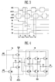
- FIG. 2 schematically illustrates the emission control line driver illustrated as part of the organic light emitting display of FIG. 1;
- FIG. 3 is a timing diagram illustrating waveforms used to drive the stages of the display illustrated in FIG. 2;
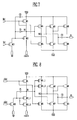
- FIG. 4 is a circuit diagram illustrating a circuit included in a stage of the display illustrated in FIG. 2;
- FIGs. 5A to 5D are circuit diagrams illustrating processes of driving the circuit illustrated in FIG. 4;
- FIG. 6 illustrates circuits included in the first to fourth stages of the driver illustrated in FIG. 2;
- FIG. 7 is a circuit diagram of another embodiment of the stage illustrated in FIG. 2;
- FIG. 8 is a circuit diagram of the stage illustrated in FIG. 2;
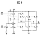
- FIG. 9 is a circuit diagram of the stage illustrated in FIG. 2..
- FIG. 1 illustrates an embodiment of an organic light emitting display.
- a scan driver 10 and an emission control line driver 30 are separate circuit elements.
- the emission control line driver 30 may be integrated with the scan driver 10.
- the organic light emitting display includes a pixel portion 40 having a plurality of pixels 50 connected to scan lines S 1 to Sn, data lines D 1 to Dm, and emission control lines E1 to En,.
- the display also includes the scan driver 10 configured to drive the scan lines S 1 to Sn, a data driver 20 configured to drive the data lines D 1 to Dm, the emission control line driver 30 configured to drive the emission control lines E1 to En, and a timing controller 60 configured to control the scan driver 10, the data driver 20, and the emission control signal driver 30.
- the scan driver 10 is controlled by the timing controller 60 such that scan driver 10sequentially supplies the scan signals to the scan lines Sl to Sn. Accordingly, the pixels 50 connected to the scan lines S1 to Sn are sequentially selected.
- the data driver 20 is controlled by the timing controller 60 so as to supply data signals to the data lines D1 to Dm during periods when the scan signals are supplied. Consequently, the data signals are supplied to the pixels 50 selected by the scan signals and the selected pixels 50 charge voltages corresponding to the data signals supplied thereto.
- the emission control line driver 30 is controlled by the timing controller 60 so as to sequentially supply the emission control signals to the emission control lines E1 to En.
- the emission control line driver 30 supplies the emission control signals so that the pixels 50 do not emit light while the data signals are supplied to the pixels 50 and so that the pixels 50 do emit light otherwise.
- the emission control line driver 30 supplies the emission control signals so that the emission control signal supplied to a jth (j is a positive integer) the emission control line Ej and the emission control signal supplied to a (j+1)th emission control line Ej+1 at least partially overlap.
- FIG. 2 schematically illustrates the emission control line driver illustrated as part of the organic light emitting display of FIG. 1;
- the emission control line driver includes n stages 321, 322, 323, 324, 325, ... configured to supply the emission control signals to the n emission control lines E 1 to En.
- the stages 321, 322, 323, 324, 325, ... are connected to the emission control lines E and are driven by two clock signals.
- the timing controller 60 supplies four clock signals Clk1, Clklb, Clk2, and Clk2b and a start signal SP to the emission control line driver 30.
- the first clock signal Clk1 and the inverted first clock signal Clklb are supplied to the odd stages 321, 323, 325, ... and the second clock signal Clk2 and the inverted second clock signal Clk2b are supplied to the even stages 322, 324, ....
- the start signal SP is supplied to the first stage 321 and the second stage 322.
- the first clock signal Clk1 and the second clock signal Clk2 have the same period and are supplied so that the high level (or low level) of the first clock signal Clk1 and the high level (or low level) of the second clock signal Clk2 overlap each other by about 1/4 period, and accordingly are about 90 degrees out of phase.
- the inverted output of an i th stage 32i (i is a positive integer) is supplied to an (i+2)th stage 32i+2 via an inverter INi. That is, the inverted output of the first stage 321 is supplied to the third stage 323 via the inverter IN1 and the inverted output of the third stage 323 is supplied to the fifth stage 325 via the inverter IN3. That is, each of the odd stages 323, 325, ... receives the inverted output of the previous odd stage.
- the inverted output of the second stage 322 is supplied to the fourth stage 324 via the inverter IN2 and the inverted output of the fourth stage 324 is supplied to the sixth stage via the inverter IN4. That is, each of the even stages 324, ... receives the inverted output of the previous even stage.
- the stages 321, 322, 323, 324, 325, ... included in the emission control line driver 30 are divided into the odd stages and the even stages.
- the stages 321, 322, 323, 324, 325, ... are driven by the two clock signals among the four clock signals supplied from the outside. That is, each of the clock signals is supplied to half of the stages in the emission control line driver 30. Accordingly, because the clock signals are supplied to only a portion of the stages included in the emission control line driver 30, the load for each clock driving circuit in the timing controller is reduced. For example, the load of the clock signals of this embodiment is reduced to about 1/2 the load for the case in which the clock signals are supplied to all of the stages.
- FIG. 2 also shows that the clock inputs of every other odd stage are connected to the first clock signal Clk1 and the inverted first clock signal Clklb in the same arrangement, while clock inputs of the other odd stages are connected to the first clock signal Clkl and the inverted first clock signal Clklb in the opposite arrangement.
- the first and second clock inputs of the first stage 321 and the fifth stage 325 are each connected to the first clock signal Clk1 and the third clock inputs of the first stage 321 and the fifth stage 325 are each connected to the inverted first clock signal Clklb.
- the first and second clock input of the third stage 323 is connected to the inverted first clock signal Clklb and the third clock input of the third stage 323 is connected to the first clock signal Clkl.
- the clock inputs of the even stages are similarly arranged with respect to the second clock signal Clk2 and the inverted second clock signal Clk2b.
- the emission control line driver 30 outputs an emission control signal every 1/4 period of each of the clock signals as illustrated in FIG. 3. Also, as illustrated in FIG. 3, two emission control signals are output while the first clock signal Clk1 maintains a high level and two emission control signals are output while the first clock signal Clk1 maintains a low level. As described above, when the emission control signal is output every 1/4 period of each of the clock signals, the emission control line driver 30 may be driven at high speed.
- FIG. 4 illustrates the internal circuit of an embodiment of each stage.
- the first stage 321 connected to the first clock signal Clk1 and the inverted first clock signal Clklb is illustrated.
- the first stage 321 includes an input unit 34 configured to generate a first signal on first node N1 in response to the clock signals Clk1 and Clklb and the start signal SP.
- the first stage 321 also includes an output unit 36 configured to generate the emission control signal in response to the first signal and the first clock signal Clk1.
- the input unit 34 includes a first transistor M1 connected to a first power source VDD and the first input terminal, a third transistor M3 connected to the second input terminal and the fourth input terminal, a second transistor M2 connected to the third transistor M3 and the third input terminal, and a first capacitor C1 connected between the gate electrode of the second transistor M2 and a first electrode (a source electrode).
- the first electrode of the first transistor M1 is connected to the first power source VDD and the gate electrode of the first transistor M1 is connected to the first input terminal.
- a second electrode (a drain electrode) of the first transistor M1 is connected to the first node N1.
- the first transistor M1 is turned on when the first clock signal Clk1 is supplied to the first input terminal. In response, the first transistor M1 supplies the voltage of the first power source VDD to the first node N1.
- the first electrode of the second transistor M2 is connected to the first node N1 and the second electrode of the second transistor M2 is connected to the third input terminal.
- the gate electrode of the second transistor M2 is connected to the first electrode of the third transistor M3.
- the second transistor M2 is turned on or off according to the voltage charged in the first capacitor C1.
- the third input terminal receives the inverted first clock signal Clklb.
- the first electrode of the third transistor M3 is connected to the gate electrode of the second transistor M2 and the second electrode of the third transistor M3 is connected to the fourth input terminal SP.
- the gate electrode of the third transistor M3 is connected to the second input terminal Clk1.
- the third transistor M3 is turned on when the first clock signal Clkl is supplied to the second input terminal.
- the first capacitor C 1 is connected between the gate electrode and the first electrode of the second transistor M2.
- the first capacitor C1 stores a voltage that turns on the second transistor M2 when a low start signal SP is supplied to the fourth input terminal and does not charge a voltage otherwise.
- the output unit 36 outputs a high emission control signal when the first signal having a low level is applied to the first node N1 and outputs a low emission control signal otherwise (that is, when the first signal having a high level is supplied to the first node N1).
- the output unit 36 includes a fourth transistor M4, a sixth transistor M6, and an eighth transistor M8, a fifth transistor M5, a seventh transistor M7, and a ninth transistor M9.
- the output unit 36 also includes a second capacitor C2, which is connected between the gate electrode and the first electrode of the ninth transistor M9.
- the first electrode of the fourth transistor M4 is connected to the first power source VDD and the second electrode of the fourth transistor M4 is connected to a second node N2.
- the gate electrode of the fourth transistor M4 is connected to the first node N1.
- the first electrode of the fifth transistor M5 is connected to the second node N2 and the second electrode of the fifth transistor M5 is connected to the second power source VSS.
- the gate electrode of the fifth transistor M5 receives the first clock signal Clk1.
- the first electrode of the sixth transistor M6 is connected to the first power source VDD and the second electrode of the sixth transistor M6 is connected to the first electrode of the seventh transistor M7.
- the gate electrode of the sixth transistor M6 is connected to the second node N2.
- the first electrode of the seventh transistor M7 is connected to the second electrode of the sixth transistor M6 and the second electrode of the seventh transistor M7 is connected to the second power source VSS.
- the gate electrode of the seventh transistor M7 is connected to the first node N1.
- the first electrode of the eighth transistor M8 is connected to the first power source VDD and the second electrode of the eighth transistor M8 is connected to the emission control line E.
- the gate electrode of the eighth transistor M8 is connected to the second electrode of the sixth transistor M6.
- the first electrode of the ninth transistor M9 is connected to the emission control line E and the second electrode of the ninth transistor M9 is connected to the second power source VSS.
- the gate electrode of the ninth transistor M9 is connected to the second node N2.
- the second capacitor C2 is connected between the gate electrode and the first electrode of the ninth transistor M9.
- the second capacitor C2 affects the turn on and off of the ninth transistor M9.
- the first clock signal Clk1 is set to be in the low level and the inverted first clock signal Clklb is set to be in the high level in a first period T1.
- the first transistor M1 is turned on by the first clock signal Clkl and the third transistor M3 is turned on by the first clock signal Clk1.
- the voltage level of the first node N1 becomes the voltage level of the first power source VDD. That is, the voltage of the first signal is in the high level and is applied to the first node N1.
- the third transistor M3 is on, the voltage level of the gate electrode of the second transistor M2 becomes the low level because the start signal SP is low during the first period T1, as shown in FIG. 4.
- the first capacitor C1 stores a voltage corresponding to the difference between the voltage of the first power source VDD applied to the first node N1 and the voltage in the low level applied to the gate electrode of the second transistor M2.
- the voltage in the low level of the start signal SP may be set to the voltage of the second power source VSS, which is lower than the voltage of the first power source VDD.
- the voltage of the inverted first clock signal Clklb is high and is supplied to the first node N1.
- the high level voltage of the inverted first clock signal Clklb is set to be the same as the voltage of the first power source VDD. Accordingly, the voltage of the first node N1 is stably maintained high even when the first transistor M1 and the second transistor M2 are simultaneously on.
- the fourth transistor M4 and the seventh transistor M7 are off.
- the fifth transistor M5 is off because of the voltage stored in the second capacitor C2 although the first clock signal Clk1 maintains the low level (the process of charging a voltage in the second capacitor C2 will be described later).
- a voltage no less than VDD- ( VSS+
- the sixth transistor M6 is turned on by the low voltage applied to the second node N2 (that is, the voltage stored in the second capacitor C2.
- the voltage of the first power source VDD is supplied to the gate electrode of the eighth transistor M8.
- the eighth transistor M8 is off.
- the ninth transistor M9 is maintained on by the voltage stored in the second capacitor C2 such that the emission control line E is supplied with an output voltage of the second power source VSS. Since a voltage no less than VDD - ( VSS +
- the first clock signal Clk1 is set to be in the high level and the inverted first clock signal Clklb is set to be in the low level during a second period T2.
- the first clock signal Clk1 When the first clock signal Clk1 is set to be in the high level, as illustrated in FIG. 5C, the first transistor M1, the third transistor M3, and the fifth transistor M5 are turned off.
- the second transistor M2 is on because of the voltage stored in the first capacitor C1 during period T1. Because the second transistor M2 is on, the voltage level of the first node N1 becomes the level of the inverted first clock signal Clklb (for example, the second power source VSS), that is, the low level.
- the fourth transistor M4 and the seventh transistor M7 are turned on.
- the voltage level of the second node N2 becomes the voltage level of the first power source VDD.
- the sixth transistor M6 and the ninth transistor M9 turn off.
- the seventh transistor M7 is turned on
- the voltage level of the gate electrode of the eighth transistor M8 becomes the voltage level of the second power source VSS so that the eighth transistor M8 is turned on.
- the eighth transistor M8 is turned on, the voltage of the first power source VDD is supplied to the emission control line E. That is, the emission control signal goes high during the second period T2. Since the voltage of the first power source VDD is supplied to the both ends of the second capacitor C2 in the second period T2, the second capacitor C2 is substantially discharged.
- the first clock signal Clk1 is set to be in the low level and the inverted first clock signal Clklb is set to be in the high level during a third period T3.
- the first transistor M1, the third transistor M3, and the fifth transistor M5 are turned on by the first clock signal Clk1.
- the voltage level of the first node N1 is becomes the voltage level of the first power source VDD. That is, the voltage of the first signal is high and is applied to the first node N1.
- the third transistor M3 Because the third transistor M3 is turned on, the voltage of the start signal SP is supplied to the gate of the second transistor M2. Because the start signal SP has a high voltage (for example, the voltage of the first power source VDD) during the third period T3, the second transistor M2 is turned off. Since the voltage of both ends of the first capacitor C1 are the voltage of the first power source VDD, the first capacitor C1 is substantially discharged. Accordingly, the first capacitor C1 stores a voltage only when the start signal SP is low.
- the start signal SP has a high voltage (for example, the voltage of the first power source VDD) during the third period T3, the second transistor M2 is turned off. Since the voltage of both ends of the first capacitor C1 are the voltage of the first power source VDD, the first capacitor C1 is substantially discharged. Accordingly, the first capacitor C1 stores a voltage only when the start signal SP is low.
- the second transistor M2 is turned off, the high valued voltage of the first signal is applied to the first node N1, and the inverted first clock signal Clklb is high. Therefore, although the first node N1 is high, because the second transistor M2 is off, current does not flow from the first node N1. This results in minimized power consumption.
- the fifth transistor M5 when the fifth transistor M5 is turned on, the voltage of the second node N2 is pulled down to the voltage of VSS+
- the fourth transistor M4 and the seventh transistor M7 are turned off by the high voltage applied to the first node N1 and the sixth transistor M6 and the ninth transistor M9 are turned on by the voltage charged in the second capacitor C2.
- the sixth transistor M6 When the sixth transistor M6 is turned on, the voltage of the first power source VDD is applied to the gate electrode of the eighth transistor M8 so that the eighth transistor M8 is turned off.
- the ninth transistor M9 When the ninth transistor M9 is turned on, the voltage level of the emission control line E1 that was high during the second period T2 becomes the voltage level of the second power source VSS. Because the voltage at the second node N2 is low, the second capacitor C2 is substantially discharged. Accordingly, the voltage of the emission control line E1 is pulled down to the voltage of the second power source VSS.
- the emission control line E is supplied with a single pulse corresponding to the next pulse of first clock signal Clk1, as desired and as shown in FIG. 3.
- FIG. 6 illustrates an embodiment of the first to fourth stages of an emission control line driver.
- the first clock input and the second clock input of the first stage 321 receive the first clock signal Clk1 and the third clock input receives the inverted first clock signal Clklb.
- the fourth input terminal receives the start signal SP.
- the first clock input and the second clock input of the third stage 323 receive the inverted first clock signal Clklb and the third clock input receives the first clock signal Clk1.
- the fourth input terminal receives the inverted output signal of the first stage 321 via the inverter IN1.
- the first clock input and the second clock input of the second stage 322 receive the second clock signal Clk2 and the third clock input receives the inverted second clock signal Clk2b.
- the fourth input terminal receives the start signal SP.
- the first clock input and the second clock input of the fourth stage 324 receive the inverted second clock signal Clk2b and the third clock input receives the second clock signal Clk2.
- the fourth input terminal receives the inverted output signal of the second stage 322 via the inverter IN2.
- the first stage 321 stores a voltage in the first capacitor C1 in response to the low start signal SP supplied in the first period T1 and supplies a high emission control signal to the first emission control line E1 in the second period T2 using the stored voltage.
- the third stage 323 stores a voltage in its first capacitor C1 according to the inverted first emission control signal supplied in the second period T2 and supplies a high emission control signal to the third emission control line E3 in the third period T3 using the stored voltage. Accordingly, the inverted first emission control signal becomes a start signal for the third stage 323.
- the second stage 322 stores a voltage in its first capacitor C1 in response to the low start signal SP supplied in the second half of the first period T1 and the first half of the second period T2 (the low start signal SP is supplied to overlap the low period of the first clock signal Clk1 and the low period of the second clock signal Clk2) and supplies a high emission control signal to the second emission control line E2 in the second half of the second period T2 and the first half of the third period T3 using the stored voltage. Therefore, the high emission control signal supplied to the second emission control line E2 partially overlaps the high emission control signals supplied to each of the first emission control line E1 and the third emission control line E3.
- the fourth stage 324 receives the inverted emission control signal supplied to the second emission control line E2 via the inverter IN2 and stores a voltage in its first capacitor C1. Thus, the inverted second emission control signal becomes a start signal for the fourth stage 324.
- the fourth stage 324 supplies a high emission control signal to the fourth emission control line E4 in the second half of the third period T3 and the first half of a fourth period T4 using the voltage stored in its first capacitor C1.
- the emission control line driver 30 uses PMOS transistors, although NMOS and CMOS configurations are also possible. When PMOS transistors are exclusively used, the emission control line driver can be mounted on a panel.
- the emission control line driver 30 When the emission control line driver 30 is mounted on the panel, it is possible to reduce the size, weight, and manufacturing cost of the panel. Also, because the emission control line driver 30 generates an emission control signal every 1/4 period of each clock signal, the emission control line driver 30 can produce emission control signals for use in high speed pixel arrays.
- FIG. 7 illustrates a circuit feature included in each stage according to some embodiments.
- the structure of the first stage 321 of FIG. 7 substantially identical the structure of the stage illustrated in FIG. 4 will be omitted.
- the stage 321 with this circuit feature further include a third capacitor C3 provided between the first power source VDD and one end of the storage capacitor C1 (the terminal connected to the gate electrode of the second transistor M2).
- the third transistor M3 When the first clock signal Clk1 is in the high level, the third transistor M3 is turned off. As a result, one end of the first capacitor C1 floats.
- the voltage of the gate electrode of the second transistor M2 may change according to the parasitic capacitor such as Cgs and Cgd of the second transistor M2 in response to a change in voltage at the first node N1.
- the third capacitor C3 is provided between the first power source VDD that maintains a uniform voltage and one end of the first capacitor C1 to reduce the change in the voltage of the gate electrode of the second transistor M2.
- FIG. 8 illustrates a circuit feature included in each stage according to some embodiments.
- the discussion of structure of the stage of FIG. 8 which is substantially identical to the structure of the stage illustrated in FIG. 4 will be omitted.
- the second transistor that receives the inverted clock signal Clklb is formed as dual gates M2_1 and M2_2.
- the fourth transistor formed between the second node N2 and the first power source VDD may be formed as dual gates M4_1 and M4_2.
- the second transistor M2_1 and M2_2 is formed as dual gates
- a lower voltage change will occur on the gate of the second transistor M2_1 and M2_2 than if a second transistor were formed as a single gate. This occurs because only the gate capacitance of the second transistor M2_2 injects charge onto the gate of the second transistor M2_1 and M2, and the gate capacitance of the second transistor M2_2 is added to the capacitance of the first capacitor C1 to stabilize the gate voltage.
- the fourth transistor M4_1 and M4_2 are formed as dual gates, although the second node N2 maintains a low voltage, the amount of leakage current that flows from the first power source VDD to the second node N2 via the fourth transistor M4 is reduced, and power consumption is accordingly reduced.
- two transistors are serially formed in each of the second transistor and the fourth transistor.
- two or more transistors may be serially formed to further enhance the performance of each of the second transistor and the fourth transistor for reasons analogous to those discussed above.
- the third capacitor C3 may be formed between one terminal of the first capacitor C1 and the first power source VDD, and one or more of the second transistor M2 and the fourth transistor M4 may be formed as two or more gates.
- the emission control line driver of the embodiments described herein since all of the transistors included in the emission control line driver are realized as PMOS, the emission control line driver can be mounted on the panel so that it is possible to reduce the size, weight, and manufacturing cost of the panel. Also, because the emission control line driver according to embodiments described herein generates an emission control signal every 1/4 period of each clock signal, the emission control line driver can be used to drive high speed displays.
- stage circuits included in the emission control line driver according to embodiments described herein have active pull up and active pull down output stages, high speed stable driving is achieved. Also, since the stage circuits included in the emission control line driver according to embodiments described herein minimize static current, power consumption is reduced.
Applications Claiming Priority (1)
| Application Number | Priority Date | Filing Date | Title |
|---|---|---|---|
| KR1020050085414A KR100646992B1 (ko) | 2005-09-13 | 2005-09-13 | 발광제어선 구동부 및 이를 이용한 유기 발광 표시장치 |
Publications (3)
| Publication Number | Publication Date |
|---|---|
| EP1763003A2 true EP1763003A2 (fr) | 2007-03-14 |
| EP1763003A3 EP1763003A3 (fr) | 2009-03-04 |
| EP1763003B1 EP1763003B1 (fr) | 2014-01-08 |
Family
ID=37698295
Family Applications (1)
| Application Number | Title | Priority Date | Filing Date |
|---|---|---|---|
| EP06254758.3A Active EP1763003B1 (fr) | 2005-09-13 | 2006-09-13 | Module de commande de ligne de contrôle d'émission et affichage électroluminescent organique utilisant le module de commande de ligne de contrôle d'émission |
Country Status (3)
| Country | Link |
|---|---|
| US (1) | US8299982B2 (fr) |
| EP (1) | EP1763003B1 (fr) |
| KR (1) | KR100646992B1 (fr) |
Cited By (9)
| Publication number | Priority date | Publication date | Assignee | Title |
|---|---|---|---|---|
| EP1903552A2 (fr) | 2006-09-22 | 2008-03-26 | Samsung SDI Co., Ltd. | Lecteur de capture, procédé de commande du signal de capture et affichage à diodes électroluminescentes organiques l'utilisant |
| EP2099018A1 (fr) * | 2008-03-04 | 2009-09-09 | Samsung Mobile Display Co., Ltd. | Commande d'émission et affichage électroluminescent organique l'utilisant |
| EP2814062A3 (fr) * | 2013-06-12 | 2015-04-08 | Samsung Display Co., Ltd. | Condensateur, circuit d'attaque comprenant le condensateur et dispositif d'affichage comprenant le circuit de commande |
| CN104751770A (zh) * | 2013-12-25 | 2015-07-01 | 昆山国显光电有限公司 | 发射控制驱动电路及使用该电路的有机发光显示器 |
| EP2874140A4 (fr) * | 2012-07-13 | 2016-03-09 | Boe Technology Group Co Ltd | Circuit de commande d'émission de lumière, procédé de commande d'émission de lumière et registre à décalage |
| US9311849B2 (en) | 2012-11-21 | 2016-04-12 | Shanghai Tianma Micro-electronics Co., Ltd. | Inverter, AMOLED compensation circuit and display panel |
| KR20160078743A (ko) * | 2014-12-24 | 2016-07-05 | 엘지디스플레이 주식회사 | 유기 발광 표시장치 |
| WO2016188367A1 (fr) * | 2015-05-22 | 2016-12-01 | 京东方科技集团股份有限公司 | Unité de registre à décalage et procédé de pilotage correspondant, circuit de pilotage de grille et dispositif d'affichage |
| EP3091532A4 (fr) * | 2013-12-30 | 2017-08-30 | Kunshan New Flat Panel Display Technology Center Co. Ltd | Circuit d'entraînement de balayage et dispositif d'affichage électroluminescent organique |
Families Citing this family (40)
| Publication number | Priority date | Publication date | Assignee | Title |
|---|---|---|---|---|
| TWI371018B (en) * | 2006-05-09 | 2012-08-21 | Chimei Innolux Corp | System for displaying image and driving display element method |
| JP4932415B2 (ja) | 2006-09-29 | 2012-05-16 | 株式会社半導体エネルギー研究所 | 半導体装置 |
| KR101489968B1 (ko) * | 2008-04-18 | 2015-02-04 | 삼성디스플레이 주식회사 | 유기전계발광 표시장치 |
| KR100969784B1 (ko) * | 2008-07-16 | 2010-07-13 | 삼성모바일디스플레이주식회사 | 유기전계발광표시장치 및 그의 구동방법 |
| KR100986862B1 (ko) | 2009-01-29 | 2010-10-08 | 삼성모바일디스플레이주식회사 | 발광제어선 구동부 및 이를 이용한 유기전계발광 표시장치 |
| KR101040855B1 (ko) | 2009-01-29 | 2011-06-14 | 삼성모바일디스플레이주식회사 | 발광 제어선 구동부 및 이를 이용한 유기전계발광 표시장치 |
| KR100986887B1 (ko) | 2009-02-17 | 2010-10-08 | 삼성모바일디스플레이주식회사 | 발광제어선 구동부 및 이를 이용한 유기전계발광 표시장치 |
| KR101056228B1 (ko) * | 2009-03-02 | 2011-08-11 | 삼성모바일디스플레이주식회사 | 유기전계발광 표시장치 |
| KR101142636B1 (ko) * | 2009-04-23 | 2012-05-03 | 삼성모바일디스플레이주식회사 | 유기전계발광 표시장치 및 그의 구동방법 |
| JP2010266715A (ja) * | 2009-05-15 | 2010-11-25 | Seiko Epson Corp | 電気光学装置及び電子機器 |
| KR101073556B1 (ko) | 2009-07-31 | 2011-10-17 | 삼성모바일디스플레이주식회사 | 표시 장치 |
| KR101101105B1 (ko) | 2009-11-04 | 2012-01-03 | 삼성모바일디스플레이주식회사 | 발광제어선 구동부 및 이를 이용한 유기전계발광 표시장치 |
| KR101108172B1 (ko) | 2010-03-16 | 2012-01-31 | 삼성모바일디스플레이주식회사 | 스캔 드라이버 및 이를 이용한 유기 발광 표시 장치 |
| KR101097351B1 (ko) * | 2010-05-06 | 2011-12-23 | 삼성모바일디스플레이주식회사 | 주사 구동 회로 및 이를 이용한 표시 장치 |
| KR101094286B1 (ko) | 2010-05-10 | 2011-12-19 | 삼성모바일디스플레이주식회사 | 발광 제어 구동부, 이를 이용한 발광 표시 장치, 및 발광 제어 신호 구동 방법 |
| KR101073569B1 (ko) | 2010-05-20 | 2011-10-14 | 삼성모바일디스플레이주식회사 | 발광 제어 구동부, 이를 이용한 발광 표시 장치, 및 발광 제어 신호 구동 방법 |
| KR101739575B1 (ko) | 2010-09-28 | 2017-05-25 | 삼성디스플레이 주식회사 | 주사 구동 장치 및 그 구동 방법 |
| KR101944465B1 (ko) * | 2011-01-06 | 2019-02-07 | 삼성디스플레이 주식회사 | 발광 제어선 구동부 및 이를 이용한 유기전계발광 표시장치 |
| KR101839953B1 (ko) | 2011-01-21 | 2018-03-20 | 삼성디스플레이 주식회사 | 구동 장치 및 이를 이용한 표시 장치 |
| KR101871188B1 (ko) * | 2011-02-17 | 2018-06-28 | 삼성디스플레이 주식회사 | 유기전계발광 표시장치 및 그의 구동방법 |
| KR20130000020A (ko) * | 2011-06-22 | 2013-01-02 | 삼성디스플레이 주식회사 | 스테이지 회로 및 이를 이용한 발광 제어선 구동부 |
| US9036766B2 (en) | 2012-02-29 | 2015-05-19 | Semiconductor Energy Laboratory Co., Ltd. | Semiconductor device |
| CN102760407B (zh) * | 2012-07-13 | 2015-11-25 | 京东方科技集团股份有限公司 | 发光控制电路、发光控制方法和移位寄存器 |
| CN103151010B (zh) * | 2013-02-27 | 2014-12-10 | 京东方科技集团股份有限公司 | 一种移位寄存器和显示装置 |
| KR20150141285A (ko) * | 2014-06-09 | 2015-12-18 | 삼성디스플레이 주식회사 | 게이트 구동 회로 및 이를 포함하는 유기 발광 표시 장치 |
| CN104599630B (zh) * | 2014-12-16 | 2017-04-19 | 上海天马有机发光显示技术有限公司 | 一种驱动电路及发光控制电路、显示面板、显示装置 |
| KR102287194B1 (ko) * | 2015-03-30 | 2021-08-09 | 삼성디스플레이 주식회사 | 게이트 구동회로 및 이를 포함하는 표시 장치 |
| KR102413874B1 (ko) * | 2015-07-02 | 2022-06-29 | 삼성디스플레이 주식회사 | 발광제어 구동부 및 이를 포함하는 표시장치 |
| US10777116B1 (en) * | 2015-09-25 | 2020-09-15 | Apple Inc. | Electronic display emission scanning |
| KR102330860B1 (ko) * | 2015-10-05 | 2021-11-25 | 엘지디스플레이 주식회사 | 유기발광 표시장치와 그 구동방법 |
| CN105529000B (zh) * | 2016-02-18 | 2018-01-23 | 京东方科技集团股份有限公司 | 信号生成单元、移位寄存器、显示装置及信号生成方法 |
| CN105609054B (zh) * | 2016-02-29 | 2018-05-08 | 信利(惠州)智能显示有限公司 | 一种发光控制电路及移位寄存器 |
| KR102578712B1 (ko) * | 2016-12-22 | 2023-09-15 | 엘지디스플레이 주식회사 | 발광 제어 드라이버 및 그를 이용한 유기 발광 다이오드 표시 장치 |
| KR20180096843A (ko) | 2017-02-20 | 2018-08-30 | 삼성디스플레이 주식회사 | 스테이지 회로 및 이를 이용한 주사 구동부 |
| CN107331348B (zh) * | 2017-08-31 | 2019-11-08 | 京东方科技集团股份有限公司 | 移位寄存器单元及其驱动方法、阵列基板和显示装置 |
| CN110136652B (zh) * | 2019-05-24 | 2020-10-16 | 深圳市华星光电半导体显示技术有限公司 | 一种goa电路及阵列基板 |
| CN110706656B (zh) * | 2019-10-21 | 2021-02-02 | 京东方科技集团股份有限公司 | 一种移位寄存器、其驱动方法、驱动电路及显示装置 |
| KR20210081507A (ko) * | 2019-12-23 | 2021-07-02 | 삼성디스플레이 주식회사 | 발광 구동부 및 이를 포함하는 표시 장치 |
| US11074854B1 (en) * | 2020-03-09 | 2021-07-27 | Novatek Microelectronics Corp. | Driving device and operation method thereof |
| KR20220016420A (ko) * | 2020-07-31 | 2022-02-09 | 삼성디스플레이 주식회사 | 표시 장치 |
Citations (3)
| Publication number | Priority date | Publication date | Assignee | Title |
|---|---|---|---|---|
| US5633653A (en) | 1994-08-31 | 1997-05-27 | David Sarnoff Research Center, Inc. | Simultaneous sampling of demultiplexed data and driving of an LCD pixel array with ping-pong effect |
| US20040164978A1 (en) | 2003-02-24 | 2004-08-26 | Dong-Yong Shin | Buffer circuit and active matrix display using the same |
| US20050036581A1 (en) | 2003-08-13 | 2005-02-17 | Toppoly Optoelectronics Corp. | Shift register unit and signal driving circuit using the same |
Family Cites Families (15)
| Publication number | Priority date | Publication date | Assignee | Title |
|---|---|---|---|---|
| KR100430099B1 (ko) * | 1999-03-02 | 2004-05-03 | 엘지.필립스 엘시디 주식회사 | 쉬프트 레지스터 회로 |
| US6580657B2 (en) * | 2001-01-04 | 2003-06-17 | International Business Machines Corporation | Low-power organic light emitting diode pixel circuit |
| TW582005B (en) * | 2001-05-29 | 2004-04-01 | Semiconductor Energy Lab | Pulse output circuit, shift register, and display device |
| US7050036B2 (en) * | 2001-12-12 | 2006-05-23 | Lg.Philips Lcd Co., Ltd. | Shift register with a built in level shifter |
| JP3671012B2 (ja) | 2002-03-07 | 2005-07-13 | 三洋電機株式会社 | 表示装置 |
| KR100524122B1 (ko) | 2003-06-26 | 2005-10-25 | 하나 마이크론(주) | 저소비 전력 유기 전계 발광 디바이스 디스플레이 구동 장치 |
| US7486269B2 (en) * | 2003-07-09 | 2009-02-03 | Samsung Electronics Co., Ltd. | Shift register, scan driving circuit and display apparatus having the same |
| KR100566814B1 (ko) * | 2003-07-24 | 2006-04-03 | 엘지.필립스 엘시디 주식회사 | 쉬프트 레지스터 |
| US7289594B2 (en) * | 2004-03-31 | 2007-10-30 | Lg.Philips Lcd Co., Ltd. | Shift registrer and driving method thereof |
| KR101030528B1 (ko) * | 2004-05-27 | 2011-04-26 | 엘지디스플레이 주식회사 | 쉬프트 레지스터 및 이를 사용한 액정표시장치 |
| KR100658616B1 (ko) * | 2004-05-31 | 2006-12-15 | 삼성에스디아이 주식회사 | 발광 표시 장치 및 그 표시 패널과 구동 방법 |
| US7639226B2 (en) * | 2004-05-31 | 2009-12-29 | Lg Display Co., Ltd. | Liquid crystal display panel with built-in driving circuit |
| WO2005122178A1 (fr) | 2004-06-14 | 2005-12-22 | Semiconductor Energy Laboratory Co., Ltd. | Registre à décalage et dispositif d’affichage semi-conducteur |
| KR100578812B1 (ko) * | 2004-06-29 | 2006-05-11 | 삼성에스디아이 주식회사 | 발광 표시 장치 |
| KR100846954B1 (ko) * | 2004-08-30 | 2008-07-17 | 삼성에스디아이 주식회사 | 발광 표시장치와 그의 구동방법 |
-
2005
- 2005-09-13 KR KR1020050085414A patent/KR100646992B1/ko active IP Right Grant
-
2006
- 2006-09-12 US US11/520,068 patent/US8299982B2/en active Active
- 2006-09-13 EP EP06254758.3A patent/EP1763003B1/fr active Active
Patent Citations (3)
| Publication number | Priority date | Publication date | Assignee | Title |
|---|---|---|---|---|
| US5633653A (en) | 1994-08-31 | 1997-05-27 | David Sarnoff Research Center, Inc. | Simultaneous sampling of demultiplexed data and driving of an LCD pixel array with ping-pong effect |
| US20040164978A1 (en) | 2003-02-24 | 2004-08-26 | Dong-Yong Shin | Buffer circuit and active matrix display using the same |
| US20050036581A1 (en) | 2003-08-13 | 2005-02-17 | Toppoly Optoelectronics Corp. | Shift register unit and signal driving circuit using the same |
Cited By (18)
| Publication number | Priority date | Publication date | Assignee | Title |
|---|---|---|---|---|
| EP1903552A3 (fr) * | 2006-09-22 | 2009-05-27 | Samsung Mobile Display Co., Ltd. | Lecteur de capture, procédé de commande du signal de capture et affichage à diodes électroluminescentes organiques l'utilisant |
| US8130183B2 (en) | 2006-09-22 | 2012-03-06 | Samsung Mobile Display Co., Ltd. | Scan driver and scan signal driving method and organic light emitting display using the same |
| EP1903552A2 (fr) | 2006-09-22 | 2008-03-26 | Samsung SDI Co., Ltd. | Lecteur de capture, procédé de commande du signal de capture et affichage à diodes électroluminescentes organiques l'utilisant |
| EP2099018A1 (fr) * | 2008-03-04 | 2009-09-09 | Samsung Mobile Display Co., Ltd. | Commande d'émission et affichage électroluminescent organique l'utilisant |
| JP2009211028A (ja) * | 2008-03-04 | 2009-09-17 | Samsung Mobile Display Co Ltd | エミッション駆動部及び有機電界発光表示装置 |
| CN101527110B (zh) * | 2008-03-04 | 2011-06-15 | 三星移动显示器株式会社 | 发射驱动器和利用所述发射驱动器的有机发光显示器 |
| US8339424B2 (en) | 2008-03-04 | 2012-12-25 | Samsung Display Co., Ltd. | Emission driver and organic light emitting display using the same |
| EP2874140A4 (fr) * | 2012-07-13 | 2016-03-09 | Boe Technology Group Co Ltd | Circuit de commande d'émission de lumière, procédé de commande d'émission de lumière et registre à décalage |
| US9311849B2 (en) | 2012-11-21 | 2016-04-12 | Shanghai Tianma Micro-electronics Co., Ltd. | Inverter, AMOLED compensation circuit and display panel |
| US9548025B2 (en) | 2013-06-12 | 2017-01-17 | Samsung Display Co., Ltd. | Capacitor, driving circuit comprising the capacitor, and display device comprising the driving circuit |
| EP2814062A3 (fr) * | 2013-06-12 | 2015-04-08 | Samsung Display Co., Ltd. | Condensateur, circuit d'attaque comprenant le condensateur et dispositif d'affichage comprenant le circuit de commande |
| CN104751770A (zh) * | 2013-12-25 | 2015-07-01 | 昆山国显光电有限公司 | 发射控制驱动电路及使用该电路的有机发光显示器 |
| EP3091532A4 (fr) * | 2013-12-30 | 2017-08-30 | Kunshan New Flat Panel Display Technology Center Co. Ltd | Circuit d'entraînement de balayage et dispositif d'affichage électroluminescent organique |
| US10013919B2 (en) | 2013-12-30 | 2018-07-03 | Kunshan New Flat Panel Display Technology Center Co. Ltd. | Scanning drive circuit and organic light-emitting display |
| KR101878380B1 (ko) * | 2013-12-30 | 2018-07-13 | 쿤산 뉴 플랫 패널 디스플레이 테크놀로지 센터 씨오., 엘티디. | 스캐닝 구동 회로와 유기 발광 디스플레이 |
| KR20160078743A (ko) * | 2014-12-24 | 2016-07-05 | 엘지디스플레이 주식회사 | 유기 발광 표시장치 |
| WO2016188367A1 (fr) * | 2015-05-22 | 2016-12-01 | 京东方科技集团股份有限公司 | Unité de registre à décalage et procédé de pilotage correspondant, circuit de pilotage de grille et dispositif d'affichage |
| US9786228B2 (en) | 2015-05-22 | 2017-10-10 | Boe Technology Group Co., Ltd. | Shift register unit and control method thereof, gate driving circuit, and display device |
Also Published As
| Publication number | Publication date |
|---|---|
| US8299982B2 (en) | 2012-10-30 |
| US20070063933A1 (en) | 2007-03-22 |
| EP1763003A3 (fr) | 2009-03-04 |
| EP1763003B1 (fr) | 2014-01-08 |
| KR100646992B1 (ko) | 2006-11-23 |
Similar Documents
| Publication | Publication Date | Title |
|---|---|---|
| EP1763003B1 (fr) | Module de commande de ligne de contrôle d'émission et affichage électroluminescent organique utilisant le module de commande de ligne de contrôle d'émission | |
| US11100856B2 (en) | Stage and organic light emitting display device using the same | |
| EP2099018B1 (fr) | Affichage électroluminescent organique utilisant un module de commande d'émission | |
| KR100729099B1 (ko) | 주사 구동회로와 이를 이용한 유기 전계발광 장치 | |
| US9330593B2 (en) | Stage circuit and organic light emitting display using the same | |
| US9443464B2 (en) | Stage circuit and organic light emitting display device using the same | |
| KR102061256B1 (ko) | 스테이지 회로 및 이를 이용한 유기전계발광 표시장치 | |
| US9183781B2 (en) | Stage circuit and bidirectional emission control driver using the same | |
| US8665182B2 (en) | Emission control driver and organic light emitting display device using the same | |
| US8451259B2 (en) | Emission driver and organic light emitting display device including the same | |
| US8803562B2 (en) | Stage circuit and scan driver using the same | |
| US7907104B2 (en) | Luminescent display device and method that drives the same | |
| JP7071318B2 (ja) | ゲート駆動部およびこれを用いた電界発光表示装置 | |
| KR20080027062A (ko) | 주사구동부, 주사신호의 구동방법 및 그를 이용한유기전계발광표시장치 | |
| KR20130003252A (ko) | 스테이지 회로 및 이를 이용한 주사 구동부 | |
| US8354979B2 (en) | Logic gate, scan driver and organic light emitting diode display using the same | |
| CN113066422B (zh) | 扫描与发光驱动电路、扫描与发光驱动系统、显示面板 | |
| US7528631B2 (en) | Logic gate, scan driver and organic light emitting diode display using the same | |
| US7978188B2 (en) | Data driver and organic light emitting display using the same | |
| KR102174833B1 (ko) | 게이트 구동회로 및 이를 포함한 표시장치 | |
| US20080170059A1 (en) | Buffer and organic light emitting display using the buffer | |
| KR100796125B1 (ko) | 쉬프트 레지스터 및 데이터 구동회로와 이를 이용한 유기전계발광 표시장치 | |
| US11893942B2 (en) | GOA unit circuit, driving method, GOA circuit, and display apparatus |
Legal Events
| Date | Code | Title | Description |
|---|---|---|---|
| PUAI | Public reference made under article 153(3) epc to a published international application that has entered the european phase |
Free format text: ORIGINAL CODE: 0009012 |
|
| 17P | Request for examination filed |
Effective date: 20060922 |
|
| AK | Designated contracting states |
Kind code of ref document: A2 Designated state(s): AT BE BG CH CY CZ DE DK EE ES FI FR GB GR HU IE IS IT LI LT LU LV MC NL PL PT RO SE SI SK TR |
|
| AX | Request for extension of the european patent |
Extension state: AL BA HR MK YU |
|
| PUAL | Search report despatched |
Free format text: ORIGINAL CODE: 0009013 |
|
| RAP1 | Party data changed (applicant data changed or rights of an application transferred) |
Owner name: SAMSUNG MOBILE DISPLAY CO., LTD. |
|
| AK | Designated contracting states |
Kind code of ref document: A3 Designated state(s): AT BE BG CH CY CZ DE DK EE ES FI FR GB GR HU IE IS IT LI LT LU LV MC NL PL PT RO SE SI SK TR |
|
| AX | Request for extension of the european patent |
Extension state: AL BA HR MK RS |
|
| 17Q | First examination report despatched |
Effective date: 20090717 |
|
| AKX | Designation fees paid |
Designated state(s): DE FR GB |
|
| RAP1 | Party data changed (applicant data changed or rights of an application transferred) |
Owner name: SAMSUNG DISPLAY CO., LTD. |
|
| REG | Reference to a national code |
Ref country code: DE Ref legal event code: R079 Ref document number: 602006039941 Country of ref document: DE Free format text: PREVIOUS MAIN CLASS: G09G0003000000 Ipc: G09G0003320000 |
|
| GRAP | Despatch of communication of intention to grant a patent |
Free format text: ORIGINAL CODE: EPIDOSNIGR1 |
|
| RIC1 | Information provided on ipc code assigned before grant |
Ipc: G11C 19/28 20060101ALI20130214BHEP Ipc: G09G 3/32 20060101AFI20130214BHEP Ipc: G11C 19/18 20060101ALI20130214BHEP |
|
| GRAP | Despatch of communication of intention to grant a patent |
Free format text: ORIGINAL CODE: EPIDOSNIGR1 |
|
| INTG | Intention to grant announced |
Effective date: 20131016 |
|
| GRAS | Grant fee paid |
Free format text: ORIGINAL CODE: EPIDOSNIGR3 |
|
| GRAA | (expected) grant |
Free format text: ORIGINAL CODE: 0009210 |
|
| AK | Designated contracting states |
Kind code of ref document: B1 Designated state(s): DE FR GB |
|
| REG | Reference to a national code |
Ref country code: GB Ref legal event code: FG4D |
|
| REG | Reference to a national code |
Ref country code: DE Ref legal event code: R096 Ref document number: 602006039941 Country of ref document: DE Effective date: 20140220 |
|
| REG | Reference to a national code |
Ref country code: DE Ref legal event code: R097 Ref document number: 602006039941 Country of ref document: DE |
|
| PLBE | No opposition filed within time limit |
Free format text: ORIGINAL CODE: 0009261 |
|
| STAA | Information on the status of an ep patent application or granted ep patent |
Free format text: STATUS: NO OPPOSITION FILED WITHIN TIME LIMIT |
|
| 26N | No opposition filed |
Effective date: 20141009 |
|
| REG | Reference to a national code |
Ref country code: DE Ref legal event code: R097 Ref document number: 602006039941 Country of ref document: DE Effective date: 20141009 |
|
| REG | Reference to a national code |
Ref country code: FR Ref legal event code: PLFP Year of fee payment: 11 |
|
| REG | Reference to a national code |
Ref country code: FR Ref legal event code: PLFP Year of fee payment: 12 |
|
| REG | Reference to a national code |
Ref country code: FR Ref legal event code: PLFP Year of fee payment: 13 |
|
| P01 | Opt-out of the competence of the unified patent court (upc) registered |
Effective date: 20230515 |
|
| PGFP | Annual fee paid to national office [announced via postgrant information from national office to epo] |
Ref country code: GB Payment date: 20230821 Year of fee payment: 18 |
|
| PGFP | Annual fee paid to national office [announced via postgrant information from national office to epo] |
Ref country code: FR Payment date: 20230821 Year of fee payment: 18 Ref country code: DE Payment date: 20230822 Year of fee payment: 18 |