EP1748478A2 - Particules d'interconnexion auto-assemblées - Google Patents
Particules d'interconnexion auto-assemblées Download PDFInfo
- Publication number
- EP1748478A2 EP1748478A2 EP20060117534 EP06117534A EP1748478A2 EP 1748478 A2 EP1748478 A2 EP 1748478A2 EP 20060117534 EP20060117534 EP 20060117534 EP 06117534 A EP06117534 A EP 06117534A EP 1748478 A2 EP1748478 A2 EP 1748478A2
- Authority
- EP
- European Patent Office
- Prior art keywords
- particles
- contact pad
- contact
- particle
- self
- Prior art date
- Legal status (The legal status is an assumption and is not a legal conclusion. Google has not performed a legal analysis and makes no representation as to the accuracy of the status listed.)
- Granted
Links
Images


Classifications
-
- H—ELECTRICITY
- H05—ELECTRIC TECHNIQUES NOT OTHERWISE PROVIDED FOR
- H05K—PRINTED CIRCUITS; CASINGS OR CONSTRUCTIONAL DETAILS OF ELECTRIC APPARATUS; MANUFACTURE OF ASSEMBLAGES OF ELECTRICAL COMPONENTS
- H05K3/00—Apparatus or processes for manufacturing printed circuits
- H05K3/30—Assembling printed circuits with electric components, e.g. with resistor
- H05K3/32—Assembling printed circuits with electric components, e.g. with resistor electrically connecting electric components or wires to printed circuits
- H05K3/321—Assembling printed circuits with electric components, e.g. with resistor electrically connecting electric components or wires to printed circuits by conductive adhesives
-
- B—PERFORMING OPERATIONS; TRANSPORTING
- B82—NANOTECHNOLOGY
- B82Y—SPECIFIC USES OR APPLICATIONS OF NANOSTRUCTURES; MEASUREMENT OR ANALYSIS OF NANOSTRUCTURES; MANUFACTURE OR TREATMENT OF NANOSTRUCTURES
- B82Y30/00—Nanotechnology for materials or surface science, e.g. nanocomposites
-
- H—ELECTRICITY
- H01—ELECTRIC ELEMENTS
- H01L—SEMICONDUCTOR DEVICES NOT COVERED BY CLASS H10
- H01L21/00—Processes or apparatus adapted for the manufacture or treatment of semiconductor or solid state devices or of parts thereof
- H01L21/02—Manufacture or treatment of semiconductor devices or of parts thereof
- H01L21/04—Manufacture or treatment of semiconductor devices or of parts thereof the devices having at least one potential-jump barrier or surface barrier, e.g. PN junction, depletion layer or carrier concentration layer
- H01L21/48—Manufacture or treatment of parts, e.g. containers, prior to assembly of the devices, using processes not provided for in a single one of the subgroups H01L21/06 - H01L21/326
- H01L21/4814—Conductive parts
- H01L21/4846—Leads on or in insulating or insulated substrates, e.g. metallisation
- H01L21/4853—Connection or disconnection of other leads to or from a metallisation, e.g. pins, wires, bumps
-
- H—ELECTRICITY
- H01—ELECTRIC ELEMENTS
- H01L—SEMICONDUCTOR DEVICES NOT COVERED BY CLASS H10
- H01L21/00—Processes or apparatus adapted for the manufacture or treatment of semiconductor or solid state devices or of parts thereof
- H01L21/67—Apparatus specially adapted for handling semiconductor or electric solid state devices during manufacture or treatment thereof; Apparatus specially adapted for handling wafers during manufacture or treatment of semiconductor or electric solid state devices or components ; Apparatus not specifically provided for elsewhere
- H01L21/683—Apparatus specially adapted for handling semiconductor or electric solid state devices during manufacture or treatment thereof; Apparatus specially adapted for handling wafers during manufacture or treatment of semiconductor or electric solid state devices or components ; Apparatus not specifically provided for elsewhere for supporting or gripping
- H01L21/6835—Apparatus specially adapted for handling semiconductor or electric solid state devices during manufacture or treatment thereof; Apparatus specially adapted for handling wafers during manufacture or treatment of semiconductor or electric solid state devices or components ; Apparatus not specifically provided for elsewhere for supporting or gripping using temporarily an auxiliary support
-
- H—ELECTRICITY
- H01—ELECTRIC ELEMENTS
- H01L—SEMICONDUCTOR DEVICES NOT COVERED BY CLASS H10
- H01L24/00—Arrangements for connecting or disconnecting semiconductor or solid-state bodies; Methods or apparatus related thereto
- H01L24/01—Means for bonding being attached to, or being formed on, the surface to be connected, e.g. chip-to-package, die-attach, "first-level" interconnects; Manufacturing methods related thereto
- H01L24/02—Bonding areas ; Manufacturing methods related thereto
- H01L24/03—Manufacturing methods
-
- H—ELECTRICITY
- H01—ELECTRIC ELEMENTS
- H01L—SEMICONDUCTOR DEVICES NOT COVERED BY CLASS H10
- H01L24/00—Arrangements for connecting or disconnecting semiconductor or solid-state bodies; Methods or apparatus related thereto
- H01L24/01—Means for bonding being attached to, or being formed on, the surface to be connected, e.g. chip-to-package, die-attach, "first-level" interconnects; Manufacturing methods related thereto
- H01L24/02—Bonding areas ; Manufacturing methods related thereto
- H01L24/04—Structure, shape, material or disposition of the bonding areas prior to the connecting process
- H01L24/05—Structure, shape, material or disposition of the bonding areas prior to the connecting process of an individual bonding area
-
- H—ELECTRICITY
- H01—ELECTRIC ELEMENTS
- H01L—SEMICONDUCTOR DEVICES NOT COVERED BY CLASS H10
- H01L24/00—Arrangements for connecting or disconnecting semiconductor or solid-state bodies; Methods or apparatus related thereto
- H01L24/01—Means for bonding being attached to, or being formed on, the surface to be connected, e.g. chip-to-package, die-attach, "first-level" interconnects; Manufacturing methods related thereto
- H01L24/10—Bump connectors ; Manufacturing methods related thereto
- H01L24/11—Manufacturing methods
-
- H—ELECTRICITY
- H01—ELECTRIC ELEMENTS
- H01L—SEMICONDUCTOR DEVICES NOT COVERED BY CLASS H10
- H01L24/00—Arrangements for connecting or disconnecting semiconductor or solid-state bodies; Methods or apparatus related thereto
- H01L24/01—Means for bonding being attached to, or being formed on, the surface to be connected, e.g. chip-to-package, die-attach, "first-level" interconnects; Manufacturing methods related thereto
- H01L24/10—Bump connectors ; Manufacturing methods related thereto
- H01L24/12—Structure, shape, material or disposition of the bump connectors prior to the connecting process
-
- H—ELECTRICITY
- H01—ELECTRIC ELEMENTS
- H01L—SEMICONDUCTOR DEVICES NOT COVERED BY CLASS H10
- H01L24/00—Arrangements for connecting or disconnecting semiconductor or solid-state bodies; Methods or apparatus related thereto
- H01L24/01—Means for bonding being attached to, or being formed on, the surface to be connected, e.g. chip-to-package, die-attach, "first-level" interconnects; Manufacturing methods related thereto
- H01L24/26—Layer connectors, e.g. plate connectors, solder or adhesive layers; Manufacturing methods related thereto
- H01L24/28—Structure, shape, material or disposition of the layer connectors prior to the connecting process
- H01L24/29—Structure, shape, material or disposition of the layer connectors prior to the connecting process of an individual layer connector
-
- H—ELECTRICITY
- H01—ELECTRIC ELEMENTS
- H01L—SEMICONDUCTOR DEVICES NOT COVERED BY CLASS H10
- H01L24/00—Arrangements for connecting or disconnecting semiconductor or solid-state bodies; Methods or apparatus related thereto
- H01L24/80—Methods for connecting semiconductor or other solid state bodies using means for bonding being attached to, or being formed on, the surface to be connected
- H01L24/83—Methods for connecting semiconductor or other solid state bodies using means for bonding being attached to, or being formed on, the surface to be connected using a layer connector
-
- H—ELECTRICITY
- H01—ELECTRIC ELEMENTS
- H01L—SEMICONDUCTOR DEVICES NOT COVERED BY CLASS H10
- H01L24/00—Arrangements for connecting or disconnecting semiconductor or solid-state bodies; Methods or apparatus related thereto
- H01L24/90—Methods for connecting semiconductor or solid state bodies using means for bonding not being attached to, or not being formed on, the body surface to be connected, e.g. pressure contacts using springs or clips
-
- H—ELECTRICITY
- H01—ELECTRIC ELEMENTS
- H01L—SEMICONDUCTOR DEVICES NOT COVERED BY CLASS H10
- H01L2224/00—Indexing scheme for arrangements for connecting or disconnecting semiconductor or solid-state bodies and methods related thereto as covered by H01L24/00
- H01L2224/01—Means for bonding being attached to, or being formed on, the surface to be connected, e.g. chip-to-package, die-attach, "first-level" interconnects; Manufacturing methods related thereto
- H01L2224/02—Bonding areas; Manufacturing methods related thereto
- H01L2224/03—Manufacturing methods
- H01L2224/039—Methods of manufacturing bonding areas involving a specific sequence of method steps
- H01L2224/03912—Methods of manufacturing bonding areas involving a specific sequence of method steps the bump being used as a mask for patterning the bonding area
-
- H—ELECTRICITY
- H01—ELECTRIC ELEMENTS
- H01L—SEMICONDUCTOR DEVICES NOT COVERED BY CLASS H10
- H01L2224/00—Indexing scheme for arrangements for connecting or disconnecting semiconductor or solid-state bodies and methods related thereto as covered by H01L24/00
- H01L2224/01—Means for bonding being attached to, or being formed on, the surface to be connected, e.g. chip-to-package, die-attach, "first-level" interconnects; Manufacturing methods related thereto
- H01L2224/02—Bonding areas; Manufacturing methods related thereto
- H01L2224/04—Structure, shape, material or disposition of the bonding areas prior to the connecting process
- H01L2224/0401—Bonding areas specifically adapted for bump connectors, e.g. under bump metallisation [UBM]
-
- H—ELECTRICITY
- H01—ELECTRIC ELEMENTS
- H01L—SEMICONDUCTOR DEVICES NOT COVERED BY CLASS H10
- H01L2224/00—Indexing scheme for arrangements for connecting or disconnecting semiconductor or solid-state bodies and methods related thereto as covered by H01L24/00
- H01L2224/01—Means for bonding being attached to, or being formed on, the surface to be connected, e.g. chip-to-package, die-attach, "first-level" interconnects; Manufacturing methods related thereto
- H01L2224/02—Bonding areas; Manufacturing methods related thereto
- H01L2224/04—Structure, shape, material or disposition of the bonding areas prior to the connecting process
- H01L2224/05—Structure, shape, material or disposition of the bonding areas prior to the connecting process of an individual bonding area
- H01L2224/0554—External layer
- H01L2224/05599—Material
- H01L2224/056—Material with a principal constituent of the material being a metal or a metalloid, e.g. boron [B], silicon [Si], germanium [Ge], arsenic [As], antimony [Sb], tellurium [Te] and polonium [Po], and alloys thereof
- H01L2224/05617—Material with a principal constituent of the material being a metal or a metalloid, e.g. boron [B], silicon [Si], germanium [Ge], arsenic [As], antimony [Sb], tellurium [Te] and polonium [Po], and alloys thereof the principal constituent melting at a temperature of greater than or equal to 400°C and less than 950°C
- H01L2224/05624—Aluminium [Al] as principal constituent
-
- H—ELECTRICITY
- H01—ELECTRIC ELEMENTS
- H01L—SEMICONDUCTOR DEVICES NOT COVERED BY CLASS H10
- H01L2224/00—Indexing scheme for arrangements for connecting or disconnecting semiconductor or solid-state bodies and methods related thereto as covered by H01L24/00
- H01L2224/01—Means for bonding being attached to, or being formed on, the surface to be connected, e.g. chip-to-package, die-attach, "first-level" interconnects; Manufacturing methods related thereto
- H01L2224/02—Bonding areas; Manufacturing methods related thereto
- H01L2224/04—Structure, shape, material or disposition of the bonding areas prior to the connecting process
- H01L2224/05—Structure, shape, material or disposition of the bonding areas prior to the connecting process of an individual bonding area
- H01L2224/0554—External layer
- H01L2224/05599—Material
- H01L2224/056—Material with a principal constituent of the material being a metal or a metalloid, e.g. boron [B], silicon [Si], germanium [Ge], arsenic [As], antimony [Sb], tellurium [Te] and polonium [Po], and alloys thereof
- H01L2224/05638—Material with a principal constituent of the material being a metal or a metalloid, e.g. boron [B], silicon [Si], germanium [Ge], arsenic [As], antimony [Sb], tellurium [Te] and polonium [Po], and alloys thereof the principal constituent melting at a temperature of greater than or equal to 950°C and less than 1550°C
- H01L2224/05644—Gold [Au] as principal constituent
-
- H—ELECTRICITY
- H01—ELECTRIC ELEMENTS
- H01L—SEMICONDUCTOR DEVICES NOT COVERED BY CLASS H10
- H01L2224/00—Indexing scheme for arrangements for connecting or disconnecting semiconductor or solid-state bodies and methods related thereto as covered by H01L24/00
- H01L2224/01—Means for bonding being attached to, or being formed on, the surface to be connected, e.g. chip-to-package, die-attach, "first-level" interconnects; Manufacturing methods related thereto
- H01L2224/02—Bonding areas; Manufacturing methods related thereto
- H01L2224/04—Structure, shape, material or disposition of the bonding areas prior to the connecting process
- H01L2224/05—Structure, shape, material or disposition of the bonding areas prior to the connecting process of an individual bonding area
- H01L2224/0554—External layer
- H01L2224/05599—Material
- H01L2224/056—Material with a principal constituent of the material being a metal or a metalloid, e.g. boron [B], silicon [Si], germanium [Ge], arsenic [As], antimony [Sb], tellurium [Te] and polonium [Po], and alloys thereof
- H01L2224/05638—Material with a principal constituent of the material being a metal or a metalloid, e.g. boron [B], silicon [Si], germanium [Ge], arsenic [As], antimony [Sb], tellurium [Te] and polonium [Po], and alloys thereof the principal constituent melting at a temperature of greater than or equal to 950°C and less than 1550°C
- H01L2224/05647—Copper [Cu] as principal constituent
-
- H—ELECTRICITY
- H01—ELECTRIC ELEMENTS
- H01L—SEMICONDUCTOR DEVICES NOT COVERED BY CLASS H10
- H01L2224/00—Indexing scheme for arrangements for connecting or disconnecting semiconductor or solid-state bodies and methods related thereto as covered by H01L24/00
- H01L2224/01—Means for bonding being attached to, or being formed on, the surface to be connected, e.g. chip-to-package, die-attach, "first-level" interconnects; Manufacturing methods related thereto
- H01L2224/10—Bump connectors; Manufacturing methods related thereto
- H01L2224/11—Manufacturing methods
- H01L2224/113—Manufacturing methods by local deposition of the material of the bump connector
- H01L2224/1133—Manufacturing methods by local deposition of the material of the bump connector in solid form
- H01L2224/11332—Manufacturing methods by local deposition of the material of the bump connector in solid form using a powder
-
- H—ELECTRICITY
- H01—ELECTRIC ELEMENTS
- H01L—SEMICONDUCTOR DEVICES NOT COVERED BY CLASS H10
- H01L2224/00—Indexing scheme for arrangements for connecting or disconnecting semiconductor or solid-state bodies and methods related thereto as covered by H01L24/00
- H01L2224/01—Means for bonding being attached to, or being formed on, the surface to be connected, e.g. chip-to-package, die-attach, "first-level" interconnects; Manufacturing methods related thereto
- H01L2224/10—Bump connectors; Manufacturing methods related thereto
- H01L2224/11—Manufacturing methods
- H01L2224/113—Manufacturing methods by local deposition of the material of the bump connector
- H01L2224/1133—Manufacturing methods by local deposition of the material of the bump connector in solid form
- H01L2224/11334—Manufacturing methods by local deposition of the material of the bump connector in solid form using preformed bumps
-
- H—ELECTRICITY
- H01—ELECTRIC ELEMENTS
- H01L—SEMICONDUCTOR DEVICES NOT COVERED BY CLASS H10
- H01L2224/00—Indexing scheme for arrangements for connecting or disconnecting semiconductor or solid-state bodies and methods related thereto as covered by H01L24/00
- H01L2224/01—Means for bonding being attached to, or being formed on, the surface to be connected, e.g. chip-to-package, die-attach, "first-level" interconnects; Manufacturing methods related thereto
- H01L2224/10—Bump connectors; Manufacturing methods related thereto
- H01L2224/11—Manufacturing methods
- H01L2224/114—Manufacturing methods by blanket deposition of the material of the bump connector
- H01L2224/1143—Manufacturing methods by blanket deposition of the material of the bump connector in solid form
- H01L2224/11442—Manufacturing methods by blanket deposition of the material of the bump connector in solid form using a powder
-
- H—ELECTRICITY
- H01—ELECTRIC ELEMENTS
- H01L—SEMICONDUCTOR DEVICES NOT COVERED BY CLASS H10
- H01L2224/00—Indexing scheme for arrangements for connecting or disconnecting semiconductor or solid-state bodies and methods related thereto as covered by H01L24/00
- H01L2224/01—Means for bonding being attached to, or being formed on, the surface to be connected, e.g. chip-to-package, die-attach, "first-level" interconnects; Manufacturing methods related thereto
- H01L2224/10—Bump connectors; Manufacturing methods related thereto
- H01L2224/11—Manufacturing methods
- H01L2224/1147—Manufacturing methods using a lift-off mask
- H01L2224/1148—Permanent masks, i.e. masks left in the finished device, e.g. passivation layers
-
- H—ELECTRICITY
- H01—ELECTRIC ELEMENTS
- H01L—SEMICONDUCTOR DEVICES NOT COVERED BY CLASS H10
- H01L2224/00—Indexing scheme for arrangements for connecting or disconnecting semiconductor or solid-state bodies and methods related thereto as covered by H01L24/00
- H01L2224/01—Means for bonding being attached to, or being formed on, the surface to be connected, e.g. chip-to-package, die-attach, "first-level" interconnects; Manufacturing methods related thereto
- H01L2224/10—Bump connectors; Manufacturing methods related thereto
- H01L2224/11—Manufacturing methods
- H01L2224/118—Post-treatment of the bump connector
- H01L2224/1182—Applying permanent coating, e.g. in-situ coating
-
- H—ELECTRICITY
- H01—ELECTRIC ELEMENTS
- H01L—SEMICONDUCTOR DEVICES NOT COVERED BY CLASS H10
- H01L2224/00—Indexing scheme for arrangements for connecting or disconnecting semiconductor or solid-state bodies and methods related thereto as covered by H01L24/00
- H01L2224/01—Means for bonding being attached to, or being formed on, the surface to be connected, e.g. chip-to-package, die-attach, "first-level" interconnects; Manufacturing methods related thereto
- H01L2224/10—Bump connectors; Manufacturing methods related thereto
- H01L2224/11—Manufacturing methods
- H01L2224/119—Methods of manufacturing bump connectors involving a specific sequence of method steps
- H01L2224/11901—Methods of manufacturing bump connectors involving a specific sequence of method steps with repetition of the same manufacturing step
-
- H—ELECTRICITY
- H01—ELECTRIC ELEMENTS
- H01L—SEMICONDUCTOR DEVICES NOT COVERED BY CLASS H10
- H01L2224/00—Indexing scheme for arrangements for connecting or disconnecting semiconductor or solid-state bodies and methods related thereto as covered by H01L24/00
- H01L2224/01—Means for bonding being attached to, or being formed on, the surface to be connected, e.g. chip-to-package, die-attach, "first-level" interconnects; Manufacturing methods related thereto
- H01L2224/10—Bump connectors; Manufacturing methods related thereto
- H01L2224/12—Structure, shape, material or disposition of the bump connectors prior to the connecting process
- H01L2224/13—Structure, shape, material or disposition of the bump connectors prior to the connecting process of an individual bump connector
- H01L2224/13001—Core members of the bump connector
- H01L2224/1302—Disposition
- H01L2224/13022—Disposition the bump connector being at least partially embedded in the surface
-
- H—ELECTRICITY
- H01—ELECTRIC ELEMENTS
- H01L—SEMICONDUCTOR DEVICES NOT COVERED BY CLASS H10
- H01L2224/00—Indexing scheme for arrangements for connecting or disconnecting semiconductor or solid-state bodies and methods related thereto as covered by H01L24/00
- H01L2224/01—Means for bonding being attached to, or being formed on, the surface to be connected, e.g. chip-to-package, die-attach, "first-level" interconnects; Manufacturing methods related thereto
- H01L2224/10—Bump connectors; Manufacturing methods related thereto
- H01L2224/12—Structure, shape, material or disposition of the bump connectors prior to the connecting process
- H01L2224/13—Structure, shape, material or disposition of the bump connectors prior to the connecting process of an individual bump connector
- H01L2224/13001—Core members of the bump connector
- H01L2224/13075—Plural core members
- H01L2224/13078—Plural core members being disposed next to each other, e.g. side-to-side arrangements
-
- H—ELECTRICITY
- H01—ELECTRIC ELEMENTS
- H01L—SEMICONDUCTOR DEVICES NOT COVERED BY CLASS H10
- H01L2224/00—Indexing scheme for arrangements for connecting or disconnecting semiconductor or solid-state bodies and methods related thereto as covered by H01L24/00
- H01L2224/01—Means for bonding being attached to, or being formed on, the surface to be connected, e.g. chip-to-package, die-attach, "first-level" interconnects; Manufacturing methods related thereto
- H01L2224/10—Bump connectors; Manufacturing methods related thereto
- H01L2224/12—Structure, shape, material or disposition of the bump connectors prior to the connecting process
- H01L2224/13—Structure, shape, material or disposition of the bump connectors prior to the connecting process of an individual bump connector
- H01L2224/13001—Core members of the bump connector
- H01L2224/13099—Material
- H01L2224/131—Material with a principal constituent of the material being a metal or a metalloid, e.g. boron [B], silicon [Si], germanium [Ge], arsenic [As], antimony [Sb], tellurium [Te] and polonium [Po], and alloys thereof
- H01L2224/13138—Material with a principal constituent of the material being a metal or a metalloid, e.g. boron [B], silicon [Si], germanium [Ge], arsenic [As], antimony [Sb], tellurium [Te] and polonium [Po], and alloys thereof the principal constituent melting at a temperature of greater than or equal to 950°C and less than 1550°C
- H01L2224/13144—Gold [Au] as principal constituent
-
- H—ELECTRICITY
- H01—ELECTRIC ELEMENTS
- H01L—SEMICONDUCTOR DEVICES NOT COVERED BY CLASS H10
- H01L2224/00—Indexing scheme for arrangements for connecting or disconnecting semiconductor or solid-state bodies and methods related thereto as covered by H01L24/00
- H01L2224/01—Means for bonding being attached to, or being formed on, the surface to be connected, e.g. chip-to-package, die-attach, "first-level" interconnects; Manufacturing methods related thereto
- H01L2224/10—Bump connectors; Manufacturing methods related thereto
- H01L2224/12—Structure, shape, material or disposition of the bump connectors prior to the connecting process
- H01L2224/13—Structure, shape, material or disposition of the bump connectors prior to the connecting process of an individual bump connector
- H01L2224/1354—Coating
- H01L2224/1357—Single coating layer
-
- H—ELECTRICITY
- H01—ELECTRIC ELEMENTS
- H01L—SEMICONDUCTOR DEVICES NOT COVERED BY CLASS H10
- H01L2224/00—Indexing scheme for arrangements for connecting or disconnecting semiconductor or solid-state bodies and methods related thereto as covered by H01L24/00
- H01L2224/01—Means for bonding being attached to, or being formed on, the surface to be connected, e.g. chip-to-package, die-attach, "first-level" interconnects; Manufacturing methods related thereto
- H01L2224/10—Bump connectors; Manufacturing methods related thereto
- H01L2224/12—Structure, shape, material or disposition of the bump connectors prior to the connecting process
- H01L2224/13—Structure, shape, material or disposition of the bump connectors prior to the connecting process of an individual bump connector
- H01L2224/1354—Coating
- H01L2224/13599—Material
- H01L2224/136—Material with a principal constituent of the material being a metal or a metalloid, e.g. boron [B], silicon [Si], germanium [Ge], arsenic [As], antimony [Sb], tellurium [Te] and polonium [Po], and alloys thereof
-
- H—ELECTRICITY
- H01—ELECTRIC ELEMENTS
- H01L—SEMICONDUCTOR DEVICES NOT COVERED BY CLASS H10
- H01L2224/00—Indexing scheme for arrangements for connecting or disconnecting semiconductor or solid-state bodies and methods related thereto as covered by H01L24/00
- H01L2224/01—Means for bonding being attached to, or being formed on, the surface to be connected, e.g. chip-to-package, die-attach, "first-level" interconnects; Manufacturing methods related thereto
- H01L2224/26—Layer connectors, e.g. plate connectors, solder or adhesive layers; Manufacturing methods related thereto
- H01L2224/28—Structure, shape, material or disposition of the layer connectors prior to the connecting process
- H01L2224/29—Structure, shape, material or disposition of the layer connectors prior to the connecting process of an individual layer connector
- H01L2224/29001—Core members of the layer connector
- H01L2224/29099—Material
- H01L2224/291—Material with a principal constituent of the material being a metal or a metalloid, e.g. boron [B], silicon [Si], germanium [Ge], arsenic [As], antimony [Sb], tellurium [Te] and polonium [Po], and alloys thereof
- H01L2224/29101—Material with a principal constituent of the material being a metal or a metalloid, e.g. boron [B], silicon [Si], germanium [Ge], arsenic [As], antimony [Sb], tellurium [Te] and polonium [Po], and alloys thereof the principal constituent melting at a temperature of less than 400°C
-
- H—ELECTRICITY
- H01—ELECTRIC ELEMENTS
- H01L—SEMICONDUCTOR DEVICES NOT COVERED BY CLASS H10
- H01L2224/00—Indexing scheme for arrangements for connecting or disconnecting semiconductor or solid-state bodies and methods related thereto as covered by H01L24/00
- H01L2224/01—Means for bonding being attached to, or being formed on, the surface to be connected, e.g. chip-to-package, die-attach, "first-level" interconnects; Manufacturing methods related thereto
- H01L2224/26—Layer connectors, e.g. plate connectors, solder or adhesive layers; Manufacturing methods related thereto
- H01L2224/28—Structure, shape, material or disposition of the layer connectors prior to the connecting process
- H01L2224/29—Structure, shape, material or disposition of the layer connectors prior to the connecting process of an individual layer connector
- H01L2224/29001—Core members of the layer connector
- H01L2224/29099—Material
- H01L2224/29198—Material with a principal constituent of the material being a combination of two or more materials in the form of a matrix with a filler, i.e. being a hybrid material, e.g. segmented structures, foams
- H01L2224/29298—Fillers
- H01L2224/29399—Coating material
-
- H—ELECTRICITY
- H01—ELECTRIC ELEMENTS
- H01L—SEMICONDUCTOR DEVICES NOT COVERED BY CLASS H10
- H01L2224/00—Indexing scheme for arrangements for connecting or disconnecting semiconductor or solid-state bodies and methods related thereto as covered by H01L24/00
- H01L2224/80—Methods for connecting semiconductor or other solid state bodies using means for bonding being attached to, or being formed on, the surface to be connected
- H01L2224/81—Methods for connecting semiconductor or other solid state bodies using means for bonding being attached to, or being formed on, the surface to be connected using a bump connector
- H01L2224/818—Bonding techniques
- H01L2224/81801—Soldering or alloying
-
- H—ELECTRICITY
- H01—ELECTRIC ELEMENTS
- H01L—SEMICONDUCTOR DEVICES NOT COVERED BY CLASS H10
- H01L2224/00—Indexing scheme for arrangements for connecting or disconnecting semiconductor or solid-state bodies and methods related thereto as covered by H01L24/00
- H01L2224/80—Methods for connecting semiconductor or other solid state bodies using means for bonding being attached to, or being formed on, the surface to be connected
- H01L2224/83—Methods for connecting semiconductor or other solid state bodies using means for bonding being attached to, or being formed on, the surface to be connected using a layer connector
- H01L2224/838—Bonding techniques
-
- H—ELECTRICITY
- H01—ELECTRIC ELEMENTS
- H01L—SEMICONDUCTOR DEVICES NOT COVERED BY CLASS H10
- H01L2924/00—Indexing scheme for arrangements or methods for connecting or disconnecting semiconductor or solid-state bodies as covered by H01L24/00
- H01L2924/0001—Technical content checked by a classifier
- H01L2924/00013—Fully indexed content
-
- H—ELECTRICITY
- H01—ELECTRIC ELEMENTS
- H01L—SEMICONDUCTOR DEVICES NOT COVERED BY CLASS H10
- H01L2924/00—Indexing scheme for arrangements or methods for connecting or disconnecting semiconductor or solid-state bodies as covered by H01L24/00
- H01L2924/01—Chemical elements
- H01L2924/01004—Beryllium [Be]
-
- H—ELECTRICITY
- H01—ELECTRIC ELEMENTS
- H01L—SEMICONDUCTOR DEVICES NOT COVERED BY CLASS H10
- H01L2924/00—Indexing scheme for arrangements or methods for connecting or disconnecting semiconductor or solid-state bodies as covered by H01L24/00
- H01L2924/01—Chemical elements
- H01L2924/01006—Carbon [C]
-
- H—ELECTRICITY
- H01—ELECTRIC ELEMENTS
- H01L—SEMICONDUCTOR DEVICES NOT COVERED BY CLASS H10
- H01L2924/00—Indexing scheme for arrangements or methods for connecting or disconnecting semiconductor or solid-state bodies as covered by H01L24/00
- H01L2924/01—Chemical elements
- H01L2924/01013—Aluminum [Al]
-
- H—ELECTRICITY
- H01—ELECTRIC ELEMENTS
- H01L—SEMICONDUCTOR DEVICES NOT COVERED BY CLASS H10
- H01L2924/00—Indexing scheme for arrangements or methods for connecting or disconnecting semiconductor or solid-state bodies as covered by H01L24/00
- H01L2924/01—Chemical elements
- H01L2924/01014—Silicon [Si]
-
- H—ELECTRICITY
- H01—ELECTRIC ELEMENTS
- H01L—SEMICONDUCTOR DEVICES NOT COVERED BY CLASS H10
- H01L2924/00—Indexing scheme for arrangements or methods for connecting or disconnecting semiconductor or solid-state bodies as covered by H01L24/00
- H01L2924/01—Chemical elements
- H01L2924/01019—Potassium [K]
-
- H—ELECTRICITY
- H01—ELECTRIC ELEMENTS
- H01L—SEMICONDUCTOR DEVICES NOT COVERED BY CLASS H10
- H01L2924/00—Indexing scheme for arrangements or methods for connecting or disconnecting semiconductor or solid-state bodies as covered by H01L24/00
- H01L2924/01—Chemical elements
- H01L2924/01027—Cobalt [Co]
-
- H—ELECTRICITY
- H01—ELECTRIC ELEMENTS
- H01L—SEMICONDUCTOR DEVICES NOT COVERED BY CLASS H10
- H01L2924/00—Indexing scheme for arrangements or methods for connecting or disconnecting semiconductor or solid-state bodies as covered by H01L24/00
- H01L2924/01—Chemical elements
- H01L2924/01029—Copper [Cu]
-
- H—ELECTRICITY
- H01—ELECTRIC ELEMENTS
- H01L—SEMICONDUCTOR DEVICES NOT COVERED BY CLASS H10
- H01L2924/00—Indexing scheme for arrangements or methods for connecting or disconnecting semiconductor or solid-state bodies as covered by H01L24/00
- H01L2924/01—Chemical elements
- H01L2924/0103—Zinc [Zn]
-
- H—ELECTRICITY
- H01—ELECTRIC ELEMENTS
- H01L—SEMICONDUCTOR DEVICES NOT COVERED BY CLASS H10
- H01L2924/00—Indexing scheme for arrangements or methods for connecting or disconnecting semiconductor or solid-state bodies as covered by H01L24/00
- H01L2924/01—Chemical elements
- H01L2924/01033—Arsenic [As]
-
- H—ELECTRICITY
- H01—ELECTRIC ELEMENTS
- H01L—SEMICONDUCTOR DEVICES NOT COVERED BY CLASS H10
- H01L2924/00—Indexing scheme for arrangements or methods for connecting or disconnecting semiconductor or solid-state bodies as covered by H01L24/00
- H01L2924/01—Chemical elements
- H01L2924/01046—Palladium [Pd]
-
- H—ELECTRICITY
- H01—ELECTRIC ELEMENTS
- H01L—SEMICONDUCTOR DEVICES NOT COVERED BY CLASS H10
- H01L2924/00—Indexing scheme for arrangements or methods for connecting or disconnecting semiconductor or solid-state bodies as covered by H01L24/00
- H01L2924/01—Chemical elements
- H01L2924/01047—Silver [Ag]
-
- H—ELECTRICITY
- H01—ELECTRIC ELEMENTS
- H01L—SEMICONDUCTOR DEVICES NOT COVERED BY CLASS H10
- H01L2924/00—Indexing scheme for arrangements or methods for connecting or disconnecting semiconductor or solid-state bodies as covered by H01L24/00
- H01L2924/01—Chemical elements
- H01L2924/01049—Indium [In]
-
- H—ELECTRICITY
- H01—ELECTRIC ELEMENTS
- H01L—SEMICONDUCTOR DEVICES NOT COVERED BY CLASS H10
- H01L2924/00—Indexing scheme for arrangements or methods for connecting or disconnecting semiconductor or solid-state bodies as covered by H01L24/00
- H01L2924/01—Chemical elements
- H01L2924/0105—Tin [Sn]
-
- H—ELECTRICITY
- H01—ELECTRIC ELEMENTS
- H01L—SEMICONDUCTOR DEVICES NOT COVERED BY CLASS H10
- H01L2924/00—Indexing scheme for arrangements or methods for connecting or disconnecting semiconductor or solid-state bodies as covered by H01L24/00
- H01L2924/01—Chemical elements
- H01L2924/01078—Platinum [Pt]
-
- H—ELECTRICITY
- H01—ELECTRIC ELEMENTS
- H01L—SEMICONDUCTOR DEVICES NOT COVERED BY CLASS H10
- H01L2924/00—Indexing scheme for arrangements or methods for connecting or disconnecting semiconductor or solid-state bodies as covered by H01L24/00
- H01L2924/01—Chemical elements
- H01L2924/01079—Gold [Au]
-
- H—ELECTRICITY
- H01—ELECTRIC ELEMENTS
- H01L—SEMICONDUCTOR DEVICES NOT COVERED BY CLASS H10
- H01L2924/00—Indexing scheme for arrangements or methods for connecting or disconnecting semiconductor or solid-state bodies as covered by H01L24/00
- H01L2924/013—Alloys
- H01L2924/014—Solder alloys
-
- H—ELECTRICITY
- H01—ELECTRIC ELEMENTS
- H01L—SEMICONDUCTOR DEVICES NOT COVERED BY CLASS H10
- H01L2924/00—Indexing scheme for arrangements or methods for connecting or disconnecting semiconductor or solid-state bodies as covered by H01L24/00
- H01L2924/10—Details of semiconductor or other solid state devices to be connected
- H01L2924/11—Device type
- H01L2924/14—Integrated circuits
-
- H—ELECTRICITY
- H01—ELECTRIC ELEMENTS
- H01L—SEMICONDUCTOR DEVICES NOT COVERED BY CLASS H10
- H01L2924/00—Indexing scheme for arrangements or methods for connecting or disconnecting semiconductor or solid-state bodies as covered by H01L24/00
- H01L2924/15—Details of package parts other than the semiconductor or other solid state devices to be connected
- H01L2924/151—Die mounting substrate
- H01L2924/156—Material
- H01L2924/15786—Material with a principal constituent of the material being a non metallic, non metalloid inorganic material
- H01L2924/15788—Glasses, e.g. amorphous oxides, nitrides or fluorides
-
- H—ELECTRICITY
- H05—ELECTRIC TECHNIQUES NOT OTHERWISE PROVIDED FOR
- H05K—PRINTED CIRCUITS; CASINGS OR CONSTRUCTIONAL DETAILS OF ELECTRIC APPARATUS; MANUFACTURE OF ASSEMBLAGES OF ELECTRICAL COMPONENTS
- H05K2203/00—Indexing scheme relating to apparatus or processes for manufacturing printed circuits covered by H05K3/00
- H05K2203/12—Using specific substances
- H05K2203/122—Organic non-polymeric compounds, e.g. oil, wax, thiol
-
- H—ELECTRICITY
- H05—ELECTRIC TECHNIQUES NOT OTHERWISE PROVIDED FOR
- H05K—PRINTED CIRCUITS; CASINGS OR CONSTRUCTIONAL DETAILS OF ELECTRIC APPARATUS; MANUFACTURE OF ASSEMBLAGES OF ELECTRICAL COMPONENTS
- H05K3/00—Apparatus or processes for manufacturing printed circuits
- H05K3/10—Apparatus or processes for manufacturing printed circuits in which conductive material is applied to the insulating support in such a manner as to form the desired conductive pattern
- H05K3/102—Apparatus or processes for manufacturing printed circuits in which conductive material is applied to the insulating support in such a manner as to form the desired conductive pattern by bonding of conductive powder, i.e. metallic powder
Definitions
- Flat panel display assembly is a complicated process that involves coupling electronic driver chips to circuitry mounted on a glass substrate.
- COG chip-on-glass
- COG bonding often utilizes an anisotropic conducting film (ACF) tape containing a dispersion of conducting particles held together by an adhesive.
- ACF anisotropic conducting film
- bumps to the wafer is typically an expensive process that involves numerous process steps including sputtering thin metal films, photolithographic masking, electroplating and chemical etching. These methods are used to produce bumps at the fine pitches needed for displays with small pixels such as those used in portable devices. For coarser pitch bumps electroless plating avoids photolithographic masking and offers a simpler and less expensive method of bump deposition. However, electroless plating offers limited pitch and involves plating a substantial quantity of metal.
- the ACF tape is applied to bonding pads or contacts on the display edge.
- Driver chips are pressed and bonded to the other side of the ACF tape.
- Heat and pressure applied during bonding causes melting and flowing of the tape adhesive.
- particles are sandwiched between the display contacts and the driver chip contacts to form an electrical contact.
- the adhesive flowing can "wash out” some particles in the ACF film. The washed out particles can accumulate between adjacent pads and cause electrical shorts.
- a second problem results from the limited compliance of anisotropic particles in ACF tape.
- Incompressible, larger anisotropic particles can create large gaps between the driver chips and a contact pad.
- a large gap between a display contact pad and a driver chip contact can produce open adjacent contacts between an adjacent display contact pad and a corresponding adjacent driver chip contact.
- solder bumping Another type of electronic interconnection is solder bumping.
- solder bump wafer level packaging a solder bump or ball is placed onto the electrical contact pads of a wafer by electroplating, screen printing or vacuum ball placement
- solder bumps avoid ACF tape problems
- solder bump fabrication involves non-recurring engineering expenses for the creation of masks, screens or vacuum receptacles.
- a method of forming a self-assembled interconnect structure is described.
- a contact pad is formed on a substrate.
- the contact pad is exposed to a plurality of particles.
- the contact pad surface and the solution particles are selected such that at least one of the particles bonds to the contact pad. Particles that do not bond to the contact pad are subsequently removed. Pressing an opposite contact pad into the particles bonded to the contact pad forms an electrical connection between the two contact pads.
- the described method can be used to connect driver chips to display device address lines, especially address lines mounted on a transparent substrate such as glass.
- Another use for the described self-assembled interconnect structure is a replacement for solder bumping.
- the described method can be used to attach bumps either containing solder, or subsequently coated with solder to integrated circuit contact pads.
- a novel method of interconnecting electronic components uses self-assembled interconnect particles to couple electronic components together to form an electronic assembly.
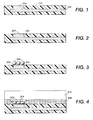
- Figures 1-4 show a basic interconnect formation process.
- an electrical contact or contact pad 104 couples to an electrical wire 108.
- wire and “electrical wire” are broadly defined as any conductor designed to carry an electrical current, including but not limited to printed and integrated circuit traces, wires and flexible interconnects.
- contact pad is broadly defined as any point to which another electrical conductor may be connected such that electricity may flow between the contact pad and the other conductor.
- the contact pad itself may be made from any conductor, but is typically made from a metal, such as gold, copper, aluminum or indium-tin oxide.
- Electrical wire or trace 108 couples contact pad 104 to additional electronic components (not shown).
- the wire may rest adjacent a substrate or be embedded in an insulating substrate 112.
- the wire or trace couples a contact pad to a display driver integrated circuit chip.
- a second wire or trace connects a second contact pad to an address line of a display system.
- the address line couples to transistors or pixel elements in the display system.
- a binding layer 204 selectively adheres to contact pad 104.
- contact pad 104 is a gold contact pad with a thiol compound binding layer.
- RSH represents an organic moiety with a substituent thiol group.
- the thiol group can react with the gold contact pad to form a covalently attached binding layer 204.
- the organothiol can react with the surface to form a layer that is the thickness of a single molecule, commonly referred to as a self-assembled monolayer.
- Example steps for aluminum and copper based pad metallurgies can include (1) Using solvents and acids to clean the pad of organics, silicon oxides, and/or nitrides, (2) Removing aluminum oxide or copper oxide with an alkaline or acid based etch, (3) activating the aluminum or copper with zincate or palladium, (4) electroless nickel plating a thin Ni layer using ammonia based plating solution and (5) Plating a thin gold layer using a cyanide or sulfate based solution.
- an optional layer may be selectively applied to substrate 112 surface, (and not to contact pad 104).
- the optional layer inhibits particle attachment to non contact pad regions.
- contact pad 104 may be rinsed to remove any non-bonded residues. The contact pad 104 may then be exposed to freely moving particles that selectively attach to the contact pad.
- freely moving is broadly defined as any particle that is not bound in a solid. Thus, “freely moving particles” may be introduced for example in an aerosol, in a particulate cloud, or in a fluid containing the particles. The fluid containing the particles may be a colloidal suspension solution or other techniques, such as agitation, may be used to keep the particles suspended in solution.
- particles as used herein, are broadly defined as solid entities ranging in size from tens of nanometers to hundreds of microns.
- Particle as used herein are made up of more than one atom and more than one molecule, thus a single atom and/or molecule by itself shall not be considered a particle. Typically, particles will be made up of well over a hundred atoms. A “Particle” as used herein shall have at least one dimension exceeding one nanometer. A “Dimension” is commonly understood to be the height, length or width of an arbitrary object positioned at an arbitrary orientation. Another way of looking at it, and a definition that is used herein, is that a dimension is the straight line distance between any two selected points on the surface of the particle.
- binding layer 204 may be at least partially removed prior to the plating step by procedures such as ultraviolet ozone exposure or oxygen plasma ashing. Directional methods for the partial removal of binding layer 204 that leave intact the binding layer portion beneath particles 304 may help to keep the particles 304 attached during transferal of the substrate into a plating bath.
- Figure 4 shows a completed interconnect structure where a second contact 404 is brought into contact with bonded particles 304.
- upper layer 412 may be part of a display and the lower contact pad 104 couples to driver chips that control the display.
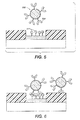
- the particles and contact pad can be coated with a layer comprising one of a pair of reactive molecules (504 and 511) (Fig 5).
- the layer on the particle comprises acetylene functional groups and the layer on the contact pad comprises azide groups. In the presence of a copper-based catalyst, these groups will bond to form a triazole through a dipolar addition reaction.
- the reactive pair comprises a carboxylic acid anhydride and an amine.
- Figure 6 shows excess particle removal using a wash step.
- wash steps might include light sonification, ozone cleaning as well as other known wash methods.
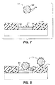
- Figure 7 illustrates using a low melting point (less than 200 degrees Centigrade) silver nanoparticles 704 attached to a microsphere 712 coating 708.
- coating 708 is a gold coating on a polymer microsphere 712.
- the contact pad surface may be treated such that silver nanoparticles 716 adhere to a metallic contact 720 but not to adjacent nitride/polymer passivation layers 724.
- Figure 8 shows nanoparticles loosely adhering to nanoparticles 716 on metallic contact 720. When heated, the nanoparticles 804 melt and fuse producing a strong bond between microsphere 712 and metallic contact 720. Microspheres on passivation layers 724 form a weak, easily broken adhesion that breaks during washing.
- Figures 6-8 show chemical techniques of placing and forming bonds, however interconnect self assembly should not be limited to chemical bonding techniques.
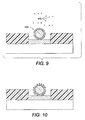
- Figures 9 and 10 show using magnetic micro-particles 904 to control the movement of smaller magnetic particles.
- Figure 9 shows a larger magnetic micro-particle 904 attached to a contact pad.
- the magnetic micro-particle could for example be a polymer sphere coated with a layer of Ni to provide magnetic properties, and a subsequent Au layer.
- Also shown in Figure 9 are smaller magnetic particles 908 in proximity to the larger particle.
- Figure 10 shows using magnetized larger particles to attract smaller particles to the larger particles.
- Application of a magnetic field induces magnetic dipoles in the particles, resulting in mutual attraction. Once brought into contact the particles stick to one another by virtue of their surface properties, and remain stuck to one another in the absence of an externally applied magnetic field.
- Figures 1-4 describe a method of forming an interconnect from a contact pad that is approximately planar with a supporting substrate.
- the described interconnect relies on adhering particles to form the contact above the surrounding substrate.
- particle sizes are too small to create sufficient spacing between the two contacting surfaces and a raised contact, often referred to as a bump, may be preferred.
- Figures 11-19 describe using self assembly techniques in conjunction with traditional fabrication techniques to form raised contact bumps. Raised contact bumps increase the spacing between substrates supporting each contact. Thus, raised contacts are particularly suitable to form a display.
- contact pad base 1108 couples to a metal conductor 1104 supported by substrate material 1112.
- display driver circuitry is typically formed on silicon wafer chips, thus silicon is a common substrate material, although other materials may also be used.
- Dielectric passivation layer 1116 protects the electronic circuitry.
- contact pad base 1108 serves as the contact pad upon which particles are deposited.
- additional contact pad material is deposited to form a raised contact bump.
- a plating cathode seed layer 1120 is formed over contact pad base 1108. Seed layer 1120 is typically made from Au but may be any material upon which a contact pad may be formed.
- Figures 12 and 13 show the formation of contact bump 1304.
- a photoresist layer 1204 is patterned around contact pad base 1108.
- a conductor material deposited in the photoresist gap forms contact bump 1304.
- Figures 14-16 illustrate the attachment of particles to the contact pad. Attachment may be done using a variety of self assembling procedures, including, but not limited to the attachment procedures described in Figures 5-10.
- a particle bonding coating 1404 is added to a contact 1304 top surface 1308. When exposed to a liquid or gas containing particles, particles 1504 adhere to bonding coating 1404 as shown in Figure 15.
- the particles 1504 may be conducting at the time they are self-assembled onto the top surface 1308.
- Conducting particles may be made from a variety of techniques used for making the particles employed in ACF tape and are commercially available for example from JCI USA Inc. (a subsidiary of Nippon Chemical Industrial Co., Ltd.) 1311 Mamaroneck Avenue, Suite 145, White Plains, NY 10605.
- These particles may consist of a core and a cladding material.
- the core material may be organic, for example polystyrene, polymethyl methacrylate, benzoguanamine, etc. or may also be inorganic for example nickel, copper, silica or graphite.
- the cladding material may be a metal, such as an Au film, or a bilayer of Au on Ni. Typical particle sizes range from 1 to 50 microns.
- the particles 1504 may also be non-conducting at the time they are self-assembled onto the top surface 1308.
- two and three dimensional colloidal crystals can be assembled from organic particles, (polystyrene, latex) inorganic particles (silicon oxides) and biomolecules (proteins, DNA). Typical particles sizes range from 5 nm to 5mm.
- Lee et. al, Adv. Mater. 2002, 14, No. 8 pp. 572-7 describes the formation of clusters of carboxylated latex spheres that self-organize onto patterned polymer multilayers.
- it is possible to self-assemble non conducting particles for example SiO2 or polystyrene
- selective electroless metal plating on to the particles.
- bonding particles 1504 to bonding coating 1404 may be used.
- hydrophobic particles such as latex or teflon are suspended in a hydrophilic (aqueous) solution. Bonding coating 1404 produces a hydrophobic region that attracts the hydrophobic particles out of the aqueous solution.
- the structure of Figure 13 is exposed to a bath containing thiol compounds, usually with a general formula RSH, that have a high affinity for gold.
- thiol compounds usually with a general formula RSH, that have a high affinity for gold.
- contact bump 1304 is made from gold
- the thiol compounds adhere to the gold contact pad.
- Rinsing the wafer removes the thiol compound from other wafer regions including photoresist layer 1204.
- the wafer is then exposed to a solution containing a colloidal suspension of gold surfaced particles. The gold surfaced particles then bond to the thiol bonding layer, but not to the other wafer regions.
- conducting anchoring or bonding molecules facilitates the plating step that reinforces the attachment of a particle to its respective bump or pad.
- a conducting polymer comprising a poly(thiophene) backbone and sidechains comprising chemically binding functionalities, such as thiols or amines, can be used to form the binding layer 1404 on the contact pad 1304.
- the binding layer 1404 can be composed of an electroplated conducting polymer.
- Appropriate conducting polymers include those based on ethylenedioxythiophene known as PEDOT. Electrochemical methods to form films of PEDOT derivatives are known and may also be used.
- bonding coating 1404 is at least partially removed.
- additional metal plating of the particles 1504 can further anchor the particles to the contact bump.
- the plating forms an electroless plated or electroplated metal connection between the particles 1504 and the bump 1304. The plating firmly anchors particles 1504 to the top of bump 1304, but not to the sides of the bump.
- the plating forms a conformal layer 1508 on the bump and the particles on the bump.
- a conformal layer is broadly defined as a coating or layer in which the growth is non-directional.
- a conformal layer is usually of relatively uniform thickness because the layers typically grow an approximately equal rate upon all surfaces to which the conformal layer grows (or bonds). Thus the contours of the bump and the particles is typically maintained.
- This conformal layer 1508 forms substantially a continuous coating over the contact bump surface and particle surface exposed to the plating bath. As a result, the particles 1504 become joined to bump 1304 both mechanically and electrically.
- plating only occurs where current can flow, that is where there is a conducting path to the plating electrodes attached to the substrate.
- plating only occurs on surfaces where the plating solution reacts. Typically, this reaction is limited to materials in the contact area (the contact itself and the particles bonded to the contact).
- contact pad 1904 mounts on a glass substrate 1908 and couples to display address or data lines.
- the address lines may couple to electronics or circuit elements such as thin film transistors (TFTs) in a liquid crystal display or other pixel elements that change light transmissivity, light output or light reflectivity in a display system.
- Driver circuitry such as circuitry on a video processing card to control switching the pixel elements couples to contact bump 1304.
- FIG. 18-19 shows an elevated contact bump 1304 that rises above the substrate surface. Elevated contact pads are not always necessary, as shown in the more generic example of Figure 4. Elevated contact pads provide additional tolerances, but also are more difficult to fabricate. Using larger particles such as shown in Figures 20-22 minimizes the need for elevated contact pads. Figures 20-22 show use of a large solder ball as the "conducting particle.”
- Figures 20-22 may be used to place solder bumps or balls onto substrates and chips.
- a gold surfaced solder ball may be used for self-assembly since as previously described, there are many surface treatments for promoting the self-assembly of particles with gold surfaces.
- a surface treatment 2004 applied to contact 2008 may hold solder ball 2103 in place.
- Figure 21 shows surface treatment 2004 causing solder ball 2103 to adhere to contact 2008. Once solder ball 2103 is attached, heating to reflow the solder tightens the solder-contact pad bond as shown in Figure 22.
- the described method for attaching solder may be used in cooperation with standard surface mount technology (SMT) processes to attach components to a printed circuit board.
- SMT surface mount technology
- the described process minimizes non-recurring engineering cost, in particular, the engineering cost associated with creating a screening stencil or a plating mask.
- particles used during self-assembled interconnect fabrication may be the same particles used in making anisotropic conducting film (ACF) tape. However, it is not necessary that such particles be used, nor are the particles necessarily spherical. Specially made elliptical shapes, anisotropic shapes, pyramidal shapes and as well as other shapes with pointed tips may also be used. Pointed tips may provide crushable or compliant structures designed to improve electrical contact when the second contact pad sandwiches the particles between the first contact pad and the second contact pad. Larger elastomer filled particles that are more compliant than typical smaller particles may be particularly desirable. In particular, when a 20 micron pad-pitch chip on glass structure is desired, it may be particularly useful to have pads that are approximately 10 microns in size and pads that rise approximately 10 microns.
- Figures 23-28 show one method for forming specialized particles.
- a release layer 2304 and seed layer 2302 are applied to a substrate 2308.
- Substrate 2308 includes pits 2312 in the desired particle shape.
- pyramidal shaped pits may be formed on a silicon substrate by anisotropic silicon etching using etchants such as potassium hydroxide.
- a patterned photoresist 2404 defines where particles will be located.
- Figure 25 shows particles 2504 plated into substrate 2308 pits 2312.
- Figure 26 shows photoresist 2404 removal.
- the exposed particles 2504 surface are planarized using techniques such as chemical mechanical polishing. Excess seed metal layers are etched away (this step not shawn), In one embodiment, the etch exposes a different material in particle 2504 bottom surfaces 2704 compared to other particle surfaces. The different materials exposed on different surfaces makes possible selective adherence of the bottom surface to contact pad bonding surfaces.
- the particle orientation may be controlled during self assembly.
- a pyramid structure may be designed such that the pyramid base is made of a different material such that only the pyramid base adheres to the contact pad. Thus the pyramid self-assembles such that a crushable pyramid tip usually orients upwards.
- a release etch releases the particles 2504 from the substrate. The particles may then be collected and used in previously described self-assembly processes.
- Different size particles may be used during interconnect fabrication.
- a first size of larger particles creates a bump that is elevated above the substrate surface.
- Introduction of smaller sized particles coarsens the surface providing penetrating asperities that make or improve electrical contact.
- the second size particles function in a fashion analogous to the particles that are embedded in an anisotropic conducting film (ACF) used for chip on glass bonding.
- Figures 29-34 show a system to self-assemble both the bump structure as well as the contact pressure concentrating asperities.
- Figure 29-32 shows the formation of a raised bump structure by self assembling a raised bump structure onto a contact pad.
- Figure 29 shows the formation of a contact pad 2904 while
- Figure 30 shows the deposition of a bonding layer 3004 onto the contact pad 2904.
- a large particle 3104 with a surface that has a chemical affinity for bonding layer 3004 adheres to bonding layer 3004 in figure 31.
- a number of mechanisms for such chemical affinity have been previously described, including but not limited to poly(thiophene) - thiol and amine interactions.
- large particles 3104 are optionally plated in place, for example by immersing the structure in an electroless plating bath, creating a conformal layer of metal 3204 over the particle and pad.
- a second particle bonding layer (not shown) is then applied to the plated surface.
- Figure 33 shows a smaller second set of particles 3304 "self assembling" or bonding to said second particle bonding layer.
- the smaller particles are typically 1 to 10 micrometers in diameter.
- Figure 34 shows optionally plating the smaller particles in place by forming an additional conformal plated metal layer 3404 by for example the method of electroless plating.
- the shown structure provides a completely self-assembled "contact bump" with contact pressure asperities.
- the large particle 3104 may first be covered with and bonded to smaller particles prior to bonding to the contact pad.
- the large "bump” particle is covered with smaller “contact asperity” particles to form a "coarse bump structure”
- the entire coarse bump structure is self-assembled onto the contact pad.
Applications Claiming Priority (1)
| Application Number | Priority Date | Filing Date | Title |
|---|---|---|---|
| US11/191,435 US7662708B2 (en) | 2005-07-27 | 2005-07-27 | Self-assembled interconnection particles |
Publications (3)
| Publication Number | Publication Date |
|---|---|
| EP1748478A2 true EP1748478A2 (fr) | 2007-01-31 |
| EP1748478A3 EP1748478A3 (fr) | 2007-05-09 |
| EP1748478B1 EP1748478B1 (fr) | 2019-05-01 |
Family
ID=37441343
Family Applications (1)
| Application Number | Title | Priority Date | Filing Date |
|---|---|---|---|
| EP06117534.5A Expired - Fee Related EP1748478B1 (fr) | 2005-07-27 | 2006-07-20 | Particules d'interconnexion auto-assemblées |
Country Status (5)
| Country | Link |
|---|---|
| US (1) | US7662708B2 (fr) |
| EP (1) | EP1748478B1 (fr) |
| JP (1) | JP4948067B2 (fr) |
| KR (1) | KR101262685B1 (fr) |
| TW (1) | TWI425582B (fr) |
Cited By (2)
| Publication number | Priority date | Publication date | Assignee | Title |
|---|---|---|---|---|
| WO2007113182A1 (fr) * | 2006-03-31 | 2007-10-11 | Siemens Aktiengesellschaft | procédé pour appliquer des particules de brasure sur des surfaces de contact, particules de brasure convenant dans ce but et composants dotés de surfaces de contact |
| GB2523983A (en) * | 2013-12-17 | 2015-09-16 | Conpart As | Bonded assemblies with pre-deposited polymer balls on demarcated areas and methods of forming such bonded assemblies |
Families Citing this family (13)
| Publication number | Priority date | Publication date | Assignee | Title |
|---|---|---|---|---|
| US7550846B2 (en) * | 2005-12-21 | 2009-06-23 | Palo Alto Research Center | Conductive bump with a plurality of contact elements |
| US7749327B2 (en) * | 2007-11-01 | 2010-07-06 | Micron Technology, Inc. | Methods for treating surfaces |
| US8618647B2 (en) | 2011-08-01 | 2013-12-31 | Tessera, Inc. | Packaged microelectronic elements having blind vias for heat dissipation |
| EP2701189B1 (fr) * | 2012-08-24 | 2016-01-20 | Imec | Substrat, méthode de préparation de ce substrat, procédé d'auto-assemblage de tels substrats et dispositif ainsi obtenu |
| KR102006637B1 (ko) | 2013-03-20 | 2019-10-01 | 한국전자통신연구원 | 범프의 형성 방법 및 이를 포함하는 반도체 소자의 형성방법 |
| JP5456214B1 (ja) * | 2013-06-12 | 2014-03-26 | 株式会社メイコー | 放熱基板の製造方法 |
| KR102032271B1 (ko) | 2013-08-09 | 2019-10-16 | 한국전자통신연구원 | 전자기기의 접합구조 |
| US9142475B2 (en) | 2013-08-13 | 2015-09-22 | Intel Corporation | Magnetic contacts |
| KR200475949Y1 (ko) * | 2014-08-28 | 2015-01-19 | 주식회사앤제이컴퍼니 | 실내오락용 블록형 패드 |
| KR102157942B1 (ko) | 2014-09-26 | 2020-09-21 | 인텔 코포레이션 | 플렉시블 패키징 아키텍처 |
| US9942986B1 (en) | 2016-09-23 | 2018-04-10 | Apple Inc. | System with field-assisted conductive adhesive bonds |
| CN110098199B (zh) * | 2019-05-05 | 2022-04-05 | 深圳市华星光电半导体显示技术有限公司 | 显示面板及显示装置 |
| DE102020124955A1 (de) * | 2020-09-24 | 2022-03-24 | Sphera Technology Gmbh | Elektronikeinheit mit einem integrierten Schaltkreis und Verfahren zu deren Herstellung |
Citations (8)
| Publication number | Priority date | Publication date | Assignee | Title |
|---|---|---|---|---|
| EP0372880A2 (fr) * | 1988-12-05 | 1990-06-13 | Hitachi Chemical Co., Ltd. | Composition pour connexion de circuits, procédé de connexion utilisant cette composition, et structure connectée de puces semi-conductrices |
| US5616206A (en) * | 1993-06-15 | 1997-04-01 | Ricoh Company, Ltd. | Method for arranging conductive particles on electrodes of substrate |
| WO2003028094A2 (fr) * | 2001-09-28 | 2003-04-03 | Hrl Laboratories, Llc | Procede de verrouillage automatique permettant l'adherence au cours du montage automatique de composants electroniques ou optiques |
| WO2003060995A2 (fr) * | 2002-01-18 | 2003-07-24 | Fraunhofer-Gesellschaft zur Förderung der angewandten Forschung e.V. | Dispositif d'interconnexion et procede pour le produire |
| US20050048697A1 (en) * | 2003-09-03 | 2005-03-03 | Industrial Technology Research Institute | Self-assembled nanometer conductive bumps and method for fabricating |
| EP1524695A2 (fr) * | 1996-12-06 | 2005-04-20 | Nanotronics, Inc. | Systèmes et dispositifs d'auto-assemblage fondés sur l'affinité pour applications photoniques et électroniques |
| US20050150684A1 (en) * | 2004-01-14 | 2005-07-14 | Nobuaki Hashimoto | Electronic device and method for producing the same |
| US20050227475A1 (en) * | 2004-03-18 | 2005-10-13 | Yu-Chih Chen | Method of conductive particles dispersing |
Family Cites Families (27)
| Publication number | Priority date | Publication date | Assignee | Title |
|---|---|---|---|---|
| JPS6045219A (ja) * | 1983-08-23 | 1985-03-11 | Toshiba Corp | アクテイブマトリクス型表示装置 |
| US5083697A (en) * | 1990-02-14 | 1992-01-28 | Difrancesco Louis | Particle-enhanced joining of metal surfaces |
| JPH04364734A (ja) * | 1991-06-12 | 1992-12-17 | Seiko Epson Corp | 突起電極の形成方法 |
| JPH0562981A (ja) * | 1991-06-18 | 1993-03-12 | Oki Electric Ind Co Ltd | 半導体素子の突起電極形成方法とその接続方法 |
| US5225966A (en) * | 1991-07-24 | 1993-07-06 | At&T Bell Laboratories | Conductive adhesive film techniques |
| JPH0669278A (ja) * | 1992-08-18 | 1994-03-11 | Toshiba Corp | 半導体素子の接続方法 |
| US5508144A (en) * | 1993-11-19 | 1996-04-16 | At&T Corp. | Process for fabricating a device |
| US5834335A (en) * | 1995-09-28 | 1998-11-10 | Texas Instruments Incorporated | Non-metallurgical connection between an integrated circuit and a circuit board or another integrated circuit |
| US6326241B1 (en) * | 1997-12-29 | 2001-12-04 | Visteon Global Technologies, Inc. | Solderless flip-chip assembly and method and material for same |
| US6569496B1 (en) * | 1998-03-30 | 2003-05-27 | International Business Machines Corporation | CVD of metals capable of receiving nickel or alloys thereof using inert contact |
| JP3696429B2 (ja) * | 1999-02-22 | 2005-09-21 | 日本化学工業株式会社 | 導電性無電解めっき粉体とその製造方法並びに該めっき粉体からなる導電性材料 |
| JP3570280B2 (ja) * | 1999-03-18 | 2004-09-29 | セイコーエプソン株式会社 | 半導体素子の突起電極構造およびその形成方法 |
| WO2002009175A2 (fr) * | 2000-07-20 | 2002-01-31 | President And Fellows Of Harvard College | Reseaux electriques auto-assembles |
| US6991958B2 (en) * | 2001-03-05 | 2006-01-31 | The Trustees Of Columbia University In The City Of New York | Solid-state electric device |
| US6417025B1 (en) * | 2001-04-02 | 2002-07-09 | Alien Technology Corporation | Integrated circuit packages assembled utilizing fluidic self-assembly |
| US6858481B2 (en) * | 2001-08-13 | 2005-02-22 | Advanced Micro Devices, Inc. | Memory device with active and passive layers |
| US6693384B1 (en) * | 2002-02-01 | 2004-02-17 | Alien Technology Corporation | Interconnect structure for electronic devices |
| AU2003302117A1 (en) * | 2002-02-01 | 2004-06-15 | William Marsh Rice University | Method of making a molecule-surface interface |
| JP4010846B2 (ja) * | 2002-03-29 | 2007-11-21 | 富士通日立プラズマディスプレイ株式会社 | フラットディスプレイパネル用前面フィルム及びこれを用いたフラットディスプレイ装置、並びに、プラズマディスプレイパネル用前面フィルム及びこれを用いたプラズマディスプレイ装置 |
| EP1553621A4 (fr) * | 2002-08-09 | 2005-08-10 | Jsr Corp | Connecteur a conductivite anisotrope, composition de pate conductrice, element de sonde, dispositif et procede d'inspection de plaquettes |
| KR100939615B1 (ko) * | 2002-12-13 | 2010-02-01 | 엘지디스플레이 주식회사 | 색재현성과 휘도를 증가시킨 반투과형 액정표시장치 및이의 구동방법 |
| US6923891B2 (en) * | 2003-01-10 | 2005-08-02 | Nanofilm Technologies International Pte Ltd. | Copper interconnects |
| US20040156177A1 (en) * | 2003-02-12 | 2004-08-12 | Matsushita Electric Industrial Co., Ltd. | Package of electronic components and method for producing the same |
| TW584934B (en) * | 2003-03-05 | 2004-04-21 | Au Optronics Corp | Method of forming a contact and structure thereof |
| US6858527B2 (en) * | 2003-04-14 | 2005-02-22 | Intel Corporation | Method to increase electromigration resistance of copper using self-assembled organic thiolate monolayers |
| JP2005054240A (ja) * | 2003-08-05 | 2005-03-03 | Fuji Photo Film Co Ltd | 導電性フィルムおよびその作製方法 |
| JP2005108870A (ja) * | 2003-09-26 | 2005-04-21 | Sekisui Chem Co Ltd | Icチップ、icチップの製造方法、半導体パッケージ及び液晶表示装置 |
-
2005
- 2005-07-27 US US11/191,435 patent/US7662708B2/en not_active Expired - Fee Related
-
2006
- 2006-07-20 EP EP06117534.5A patent/EP1748478B1/fr not_active Expired - Fee Related
- 2006-07-21 JP JP2006199453A patent/JP4948067B2/ja not_active Expired - Fee Related
- 2006-07-26 KR KR1020060070116A patent/KR101262685B1/ko active IP Right Grant
- 2006-07-26 TW TW95127201A patent/TWI425582B/zh not_active IP Right Cessation
Patent Citations (8)
| Publication number | Priority date | Publication date | Assignee | Title |
|---|---|---|---|---|
| EP0372880A2 (fr) * | 1988-12-05 | 1990-06-13 | Hitachi Chemical Co., Ltd. | Composition pour connexion de circuits, procédé de connexion utilisant cette composition, et structure connectée de puces semi-conductrices |
| US5616206A (en) * | 1993-06-15 | 1997-04-01 | Ricoh Company, Ltd. | Method for arranging conductive particles on electrodes of substrate |
| EP1524695A2 (fr) * | 1996-12-06 | 2005-04-20 | Nanotronics, Inc. | Systèmes et dispositifs d'auto-assemblage fondés sur l'affinité pour applications photoniques et électroniques |
| WO2003028094A2 (fr) * | 2001-09-28 | 2003-04-03 | Hrl Laboratories, Llc | Procede de verrouillage automatique permettant l'adherence au cours du montage automatique de composants electroniques ou optiques |
| WO2003060995A2 (fr) * | 2002-01-18 | 2003-07-24 | Fraunhofer-Gesellschaft zur Förderung der angewandten Forschung e.V. | Dispositif d'interconnexion et procede pour le produire |
| US20050048697A1 (en) * | 2003-09-03 | 2005-03-03 | Industrial Technology Research Institute | Self-assembled nanometer conductive bumps and method for fabricating |
| US20050150684A1 (en) * | 2004-01-14 | 2005-07-14 | Nobuaki Hashimoto | Electronic device and method for producing the same |
| US20050227475A1 (en) * | 2004-03-18 | 2005-10-13 | Yu-Chih Chen | Method of conductive particles dispersing |
Cited By (2)
| Publication number | Priority date | Publication date | Assignee | Title |
|---|---|---|---|---|
| WO2007113182A1 (fr) * | 2006-03-31 | 2007-10-11 | Siemens Aktiengesellschaft | procédé pour appliquer des particules de brasure sur des surfaces de contact, particules de brasure convenant dans ce but et composants dotés de surfaces de contact |
| GB2523983A (en) * | 2013-12-17 | 2015-09-16 | Conpart As | Bonded assemblies with pre-deposited polymer balls on demarcated areas and methods of forming such bonded assemblies |
Also Published As
| Publication number | Publication date |
|---|---|
| KR101262685B1 (ko) | 2013-05-15 |
| US7662708B2 (en) | 2010-02-16 |
| TWI425582B (zh) | 2014-02-01 |
| JP4948067B2 (ja) | 2012-06-06 |
| JP2007036236A (ja) | 2007-02-08 |
| KR20070014061A (ko) | 2007-01-31 |
| TW200729365A (en) | 2007-08-01 |
| EP1748478A3 (fr) | 2007-05-09 |
| US20070023907A1 (en) | 2007-02-01 |
| EP1748478B1 (fr) | 2019-05-01 |
Similar Documents
| Publication | Publication Date | Title |
|---|---|---|
| US7662708B2 (en) | Self-assembled interconnection particles | |
| US7504331B2 (en) | Method of fabricating self-assembled electrical interconnections | |
| US7525194B2 (en) | System including self-assembled interconnections | |
| EP2057006B1 (fr) | Procédé de fabrication d'un dispositif électronique | |
| KR100702743B1 (ko) | 전자 장치 및 그 제조 방법 | |
| TWI511208B (zh) | 以奈米結構連接和結合相鄰層 | |
| US20140312501A1 (en) | Non-random array anisotropic conductive film (acf) and manufacturing processes | |
| US7651021B2 (en) | Microball attachment using self-assembly for substrate bumping | |
| JP2006189430A (ja) | マイクロマシンプローブを搭載した薄膜回路及びその製造法と応用 | |
| JPH07336034A (ja) | 移転可能なハンダ運搬媒体を用いる電子デバイスの相互接続方法 | |
| KR100610988B1 (ko) | 부재의 접합 구조 및 접합 방법 | |
| JP2002501821A (ja) | 粒子の非ランダム単層にコーティングを形成する方法、及びそれによって形成された製品 | |
| EP0385787A2 (fr) | Procédé pour la fabrication d'électrodes de connexion | |
| US7163885B2 (en) | Method of migrating and fixing particles in a solution to bumps on a chip | |
| US20040244906A1 (en) | Laminated structure | |
| US20090057921A1 (en) | Flip chip for electrical function test and manufacturing method thereof | |
| JP2007073817A (ja) | 半導体装置の製造方法 | |
| GB2523983A (en) | Bonded assemblies with pre-deposited polymer balls on demarcated areas and methods of forming such bonded assemblies | |
| TWI250594B (en) | Method for self-assembling microstructure | |
| TW200930166A (en) | Flexible film and display device comprising the same | |
| US20080160177A1 (en) | Methods for electroless plating of metal traces on a substrate and devices and systems thereof | |
| JP2005347673A (ja) | 導電性ボールの搭載方法および搭載装置 | |
| CN115882319A (zh) | 一种电子器件的连接方法 | |
| JPH09160064A (ja) | 異方性シートおよび配線基板 | |
| JP2008200720A (ja) | はんだ接着材料及びはんだ供給方法 |
Legal Events
| Date | Code | Title | Description |
|---|---|---|---|
| PUAI | Public reference made under article 153(3) epc to a published international application that has entered the european phase |
Free format text: ORIGINAL CODE: 0009012 |
|
| AK | Designated contracting states |
Kind code of ref document: A2 Designated state(s): AT BE BG CH CY CZ DE DK EE ES FI FR GB GR HU IE IS IT LI LT LU LV MC NL PL PT RO SE SI SK TR |
|
| AX | Request for extension of the european patent |
Extension state: AL BA HR MK YU |
|
| PUAL | Search report despatched |
Free format text: ORIGINAL CODE: 0009013 |
|
| AK | Designated contracting states |
Kind code of ref document: A3 Designated state(s): AT BE BG CH CY CZ DE DK EE ES FI FR GB GR HU IE IS IT LI LT LU LV MC NL PL PT RO SE SI SK TR |
|
| AX | Request for extension of the european patent |
Extension state: AL BA HR MK YU |
|
| 17P | Request for examination filed |
Effective date: 20071109 |
|
| AKX | Designation fees paid |
Designated state(s): DE FR GB |
|
| 17Q | First examination report despatched |
Effective date: 20071221 |
|
| GRAP | Despatch of communication of intention to grant a patent |
Free format text: ORIGINAL CODE: EPIDOSNIGR1 |
|
| RIC1 | Information provided on ipc code assigned before grant |
Ipc: B82Y 30/00 20070131ALI20181024BHEP Ipc: H05K 3/32 20060101ALI20181024BHEP Ipc: H05K 3/10 20060101ALN20181024BHEP Ipc: H01L 21/48 20060101AFI20181024BHEP |
|
| RIC1 | Information provided on ipc code assigned before grant |
Ipc: B82Y 30/00 20110101ALI20181112BHEP Ipc: H05K 3/32 20060101ALI20181112BHEP Ipc: H05K 3/10 20060101ALN20181112BHEP Ipc: H01L 21/48 20060101AFI20181112BHEP |
|
| INTG | Intention to grant announced |
Effective date: 20181129 |
|
| RIC1 | Information provided on ipc code assigned before grant |
Ipc: H01L 21/48 20060101AFI20181112BHEP Ipc: B82Y 30/00 20110101ALI20181112BHEP Ipc: H05K 3/32 20060101ALI20181112BHEP Ipc: H05K 3/10 20060101ALN20181112BHEP |
|
| RIC1 | Information provided on ipc code assigned before grant |
Ipc: H01L 21/48 20060101AFI20181112BHEP Ipc: H05K 3/32 20060101ALI20181112BHEP Ipc: B82Y 30/00 20110101ALI20181112BHEP Ipc: H05K 3/10 20060101ALN20181112BHEP |
|
| GRAS | Grant fee paid |
Free format text: ORIGINAL CODE: EPIDOSNIGR3 |
|
| GRAA | (expected) grant |
Free format text: ORIGINAL CODE: 0009210 |
|
| AK | Designated contracting states |
Kind code of ref document: B1 Designated state(s): DE FR GB |
|
| REG | Reference to a national code |
Ref country code: GB Ref legal event code: FG4D |
|
| REG | Reference to a national code |
Ref country code: DE Ref legal event code: R096 Ref document number: 602006057859 Country of ref document: DE |
|
| REG | Reference to a national code |
Ref country code: DE Ref legal event code: R097 Ref document number: 602006057859 Country of ref document: DE |
|
| PLBE | No opposition filed within time limit |
Free format text: ORIGINAL CODE: 0009261 |
|
| STAA | Information on the status of an ep patent application or granted ep patent |
Free format text: STATUS: NO OPPOSITION FILED WITHIN TIME LIMIT |
|
| 26N | No opposition filed |
Effective date: 20200204 |
|
| PGFP | Annual fee paid to national office [announced via postgrant information from national office to epo] |
Ref country code: FR Payment date: 20200623 Year of fee payment: 15 |
|
| PGFP | Annual fee paid to national office [announced via postgrant information from national office to epo] |
Ref country code: GB Payment date: 20200624 Year of fee payment: 15 |
|
| PGFP | Annual fee paid to national office [announced via postgrant information from national office to epo] |
Ref country code: DE Payment date: 20200622 Year of fee payment: 15 |
|
| REG | Reference to a national code |
Ref country code: DE Ref legal event code: R119 Ref document number: 602006057859 Country of ref document: DE |
|
| GBPC | Gb: european patent ceased through non-payment of renewal fee |
Effective date: 20210720 |
|
| PG25 | Lapsed in a contracting state [announced via postgrant information from national office to epo] |
Ref country code: GB Free format text: LAPSE BECAUSE OF NON-PAYMENT OF DUE FEES Effective date: 20210720 Ref country code: DE Free format text: LAPSE BECAUSE OF NON-PAYMENT OF DUE FEES Effective date: 20220201 |
|
| PG25 | Lapsed in a contracting state [announced via postgrant information from national office to epo] |
Ref country code: FR Free format text: LAPSE BECAUSE OF NON-PAYMENT OF DUE FEES Effective date: 20210731 |