EP1746591A2 - Spiegelschichten aus Silberlegierung für ein optisches Aufzeichnungsmedium, Zerstäubungskathoden aus Silberlegierung hierfür und optisches Aufzeichnungsmedium - Google Patents
Spiegelschichten aus Silberlegierung für ein optisches Aufzeichnungsmedium, Zerstäubungskathoden aus Silberlegierung hierfür und optisches Aufzeichnungsmedium Download PDFInfo
- Publication number
- EP1746591A2 EP1746591A2 EP06012281A EP06012281A EP1746591A2 EP 1746591 A2 EP1746591 A2 EP 1746591A2 EP 06012281 A EP06012281 A EP 06012281A EP 06012281 A EP06012281 A EP 06012281A EP 1746591 A2 EP1746591 A2 EP 1746591A2
- Authority
- EP
- European Patent Office
- Prior art keywords
- alloy
- information recording
- optical information
- recording media
- laser
- Prior art date
- Legal status (The legal status is an assumption and is not a legal conclusion. Google has not performed a legal analysis and makes no representation as to the accuracy of the status listed.)
- Granted
Links
- 229910001316 Ag alloy Inorganic materials 0.000 title claims abstract description 96
- 230000003287 optical effect Effects 0.000 title claims abstract description 61
- 238000005477 sputtering target Methods 0.000 title claims abstract description 31
- 229910052744 lithium Inorganic materials 0.000 claims abstract description 22
- 229910052782 aluminium Inorganic materials 0.000 claims abstract description 20
- 229910052697 platinum Inorganic materials 0.000 claims abstract description 20
- 229910052688 Gadolinium Inorganic materials 0.000 claims abstract description 19
- 229910052802 copper Inorganic materials 0.000 claims abstract description 19
- 229910052749 magnesium Inorganic materials 0.000 claims abstract description 19
- 229910052763 palladium Inorganic materials 0.000 claims abstract description 19
- 229910052703 rhodium Inorganic materials 0.000 claims abstract description 19
- 229910052707 ruthenium Inorganic materials 0.000 claims abstract description 19
- 229910052725 zinc Inorganic materials 0.000 claims abstract description 19
- 229910052684 Cerium Inorganic materials 0.000 claims abstract description 18
- 229910052772 Samarium Inorganic materials 0.000 claims abstract description 18
- 229910052737 gold Inorganic materials 0.000 claims abstract description 18
- 229910052746 lanthanum Inorganic materials 0.000 claims abstract description 18
- 229910052727 yttrium Inorganic materials 0.000 claims abstract description 18
- 229910052718 tin Inorganic materials 0.000 claims abstract description 17
- 239000000203 mixture Substances 0.000 claims abstract description 16
- 229910052745 lead Inorganic materials 0.000 claims abstract description 15
- 229910052787 antimony Inorganic materials 0.000 claims abstract description 14
- 229910052779 Neodymium Inorganic materials 0.000 claims abstract description 13
- 229910052738 indium Inorganic materials 0.000 claims abstract description 12
- 229910052797 bismuth Inorganic materials 0.000 claims abstract description 11
- 229910045601 alloy Inorganic materials 0.000 claims description 24
- 239000000956 alloy Substances 0.000 claims description 24
- 238000000151 deposition Methods 0.000 claims description 10
- 230000008021 deposition Effects 0.000 claims description 10
- 241001013262 Theages Species 0.000 claims 1
- 239000010408 film Substances 0.000 description 66
- 239000010409 thin film Substances 0.000 description 48
- 238000002310 reflectometry Methods 0.000 description 41
- 238000010330 laser marking Methods 0.000 description 30
- 230000001965 increasing effect Effects 0.000 description 20
- 239000010410 layer Substances 0.000 description 16
- 239000000758 substrate Substances 0.000 description 14
- 230000003247 decreasing effect Effects 0.000 description 13
- 239000004417 polycarbonate Substances 0.000 description 9
- 229920000515 polycarbonate Polymers 0.000 description 9
- 238000005275 alloying Methods 0.000 description 7
- 230000007797 corrosion Effects 0.000 description 7
- 238000005260 corrosion Methods 0.000 description 7
- 230000007423 decrease Effects 0.000 description 6
- 238000000034 method Methods 0.000 description 6
- 229910000838 Al alloy Inorganic materials 0.000 description 4
- 239000000463 material Substances 0.000 description 4
- 238000002844 melting Methods 0.000 description 4
- 230000008018 melting Effects 0.000 description 4
- 229910000846 In alloy Inorganic materials 0.000 description 3
- 239000012790 adhesive layer Substances 0.000 description 3
- 238000005520 cutting process Methods 0.000 description 3
- 238000004519 manufacturing process Methods 0.000 description 3
- 239000007795 chemical reaction product Substances 0.000 description 2
- 238000004040 coloring Methods 0.000 description 2
- 238000002360 preparation method Methods 0.000 description 2
- 239000000047 product Substances 0.000 description 2
- 229910052710 silicon Inorganic materials 0.000 description 2
- 229910052709 silver Inorganic materials 0.000 description 2
- 229910018134 Al-Mg Inorganic materials 0.000 description 1
- 229910018467 Al—Mg Inorganic materials 0.000 description 1
- BQCADISMDOOEFD-UHFFFAOYSA-N Silver Chemical compound [Ag] BQCADISMDOOEFD-UHFFFAOYSA-N 0.000 description 1
- 229910052804 chromium Inorganic materials 0.000 description 1
- 230000000052 comparative effect Effects 0.000 description 1
- 239000002131 composite material Substances 0.000 description 1
- 239000004035 construction material Substances 0.000 description 1
- 230000006378 damage Effects 0.000 description 1
- 238000009826 distribution Methods 0.000 description 1
- 230000003028 elevating effect Effects 0.000 description 1
- 229910052733 gallium Inorganic materials 0.000 description 1
- 229910052732 germanium Inorganic materials 0.000 description 1
- 238000011835 investigation Methods 0.000 description 1
- 229910052741 iridium Inorganic materials 0.000 description 1
- 229910052742 iron Inorganic materials 0.000 description 1
- 238000001755 magnetron sputter deposition Methods 0.000 description 1
- 229910052751 metal Inorganic materials 0.000 description 1
- 239000002184 metal Substances 0.000 description 1
- 238000012986 modification Methods 0.000 description 1
- 230000004048 modification Effects 0.000 description 1
- 229910052758 niobium Inorganic materials 0.000 description 1
- 230000002093 peripheral effect Effects 0.000 description 1
- 229920003023 plastic Polymers 0.000 description 1
- 238000003825 pressing Methods 0.000 description 1
- 229910052702 rhenium Inorganic materials 0.000 description 1
- 239000004332 silver Substances 0.000 description 1
- 238000004544 sputter deposition Methods 0.000 description 1
- 229910052715 tantalum Inorganic materials 0.000 description 1
- 229910052716 thallium Inorganic materials 0.000 description 1
- 230000003685 thermal hair damage Effects 0.000 description 1
- 229910052719 titanium Inorganic materials 0.000 description 1
- 229910052726 zirconium Inorganic materials 0.000 description 1
Images
Classifications
-
- G—PHYSICS
- G11—INFORMATION STORAGE
- G11B—INFORMATION STORAGE BASED ON RELATIVE MOVEMENT BETWEEN RECORD CARRIER AND TRANSDUCER
- G11B7/00—Recording or reproducing by optical means, e.g. recording using a thermal beam of optical radiation by modifying optical properties or the physical structure, reproducing using an optical beam at lower power by sensing optical properties; Record carriers therefor
- G11B7/24—Record carriers characterised by shape, structure or physical properties, or by the selection of the material
- G11B7/26—Apparatus or processes specially adapted for the manufacture of record carriers
- G11B7/266—Sputtering or spin-coating layers
-
- G—PHYSICS
- G11—INFORMATION STORAGE
- G11B—INFORMATION STORAGE BASED ON RELATIVE MOVEMENT BETWEEN RECORD CARRIER AND TRANSDUCER
- G11B7/00—Recording or reproducing by optical means, e.g. recording using a thermal beam of optical radiation by modifying optical properties or the physical structure, reproducing using an optical beam at lower power by sensing optical properties; Record carriers therefor
- G11B7/24—Record carriers characterised by shape, structure or physical properties, or by the selection of the material
- G11B7/241—Record carriers characterised by shape, structure or physical properties, or by the selection of the material characterised by the selection of the material
- G11B7/252—Record carriers characterised by shape, structure or physical properties, or by the selection of the material characterised by the selection of the material of layers other than recording layers
- G11B7/258—Record carriers characterised by shape, structure or physical properties, or by the selection of the material characterised by the selection of the material of layers other than recording layers of reflective layers
- G11B7/259—Record carriers characterised by shape, structure or physical properties, or by the selection of the material characterised by the selection of the material of layers other than recording layers of reflective layers based on silver
-
- Y—GENERAL TAGGING OF NEW TECHNOLOGICAL DEVELOPMENTS; GENERAL TAGGING OF CROSS-SECTIONAL TECHNOLOGIES SPANNING OVER SEVERAL SECTIONS OF THE IPC; TECHNICAL SUBJECTS COVERED BY FORMER USPC CROSS-REFERENCE ART COLLECTIONS [XRACs] AND DIGESTS
- Y10—TECHNICAL SUBJECTS COVERED BY FORMER USPC
- Y10T—TECHNICAL SUBJECTS COVERED BY FORMER US CLASSIFICATION
- Y10T428/00—Stock material or miscellaneous articles
- Y10T428/21—Circular sheet or circular blank
Definitions
- the present invention relates to silver (Ag) alloy reflective films for optical information recording media, Ag alloy sputtering targets for the deposition thereof, and optical information recording media. More specifically, it relates to reflective films which have low thermal conductivities, low melting temperatures, high reflectivities, and high corrosion resistance and therefore enable marking on optical information recording media such as CDs, DVDs, Blu-ray Discs, and HD-DVDs typically using laser, such as marking of identification numbers in accordance typically to the burst cutting area (BCA) specifications, after the preparation of the media.
- the present invention also relates to sputtering targets for the deposition of the reflective films, and optical information recording media having the reflective films.
- Optical information recording media include various types, and the three main types categorized by the writing/reading system are read-only, write-once, and rewritable optical discs.
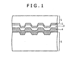
- read-only discs have recorded data formed by concave and convex pits on a transparent plastic substrate such as a polycarbonate substrate upon the manufacture of the discs, and a reflective layer mainly containing, for example, Al, Ag, or Au is arranged on the recorded data, as illustrated in FIG. 1.
- the data are read out by detecting phase difference or reflection difference of laser beam applied to the discs.
- Certain optical discs include a substrate containing recording pits and a reflective layer arranged on the recording pits, and another substrate bearing recording pits and a semi-reflective layer arranged on the recording pits. The two substrates are laminated, and the data recorded on the two layers are read out.
- FIG. 1 is a schematic view of the sectional structure of a read-only optical disc.
- the optical disc in FIG. 1 includes polycarbonate substrates 1 and 5, a semi-reflective layer (Au, Ag alloy, and Si) 2, an adhesive layer 3, and a total-reflective layer (Ag alloy) 4.
- read-only optical discs are produced in quantities, and information is recorded upon production of the discs by pressing with stampers havingpatterns of the information. Thus, IDs cannot be significantly given to individual discs.
- read-only optical discs individually having IDs formed using a dedicated system such as a label gate system or a burst cutting area (BCA) system after the preparation of the discs are being standardized typically for preventing unauthorized copying, improving traceability in distribution of products, and increasing added values of products.
- the ID marking (recording) is mainly carried out by a method of applying laser beam to discs after production to melt an Al alloy in the reflective film and to form holes therein.
- Aluminum alloys such as Al-Mg alloys according to Japanese Industrial Standards (JIS) 6061, are distributed in quantities as general construction materials, are inexpensive and are thereby widely used as reflective films of read-only optical discs.
- Ag alloys having higher reflectivities are widely used in recordable (write-once and rewritable) optical discs.
- JP-A No. 1992-252440 discloses a method for reducing the thermal conductivity of an Ag alloy by incorporating Ge, Si, Sn, Pb, Ga, In, Tl, Sb, or Bi into Ag.
- JP-A No. 1992-28032 discloses a method for reducing the thermal conductivity of an Ag alloy by incorporating Cr, Ti, Si, Ta, Nb, Pt, Ir, Fe, Re, Sb, Zr, Sn, or Ni into Ag.
- the resulting reflective films obtained according to these techniques are not intended to be melted and removed by laser irradiation, and some of them show increasing melting temperatures with decreasing thermal conductivities thereof.
- Silver alloys (Ag alloys) satisfying requirements as Ag alloys for laser marking have not yet been provided.
- the present inventors have developed Ag alloys which have improved thermal conductivities, laser-beam absorptivities, and corrosion resistance and are suitable for laser making, by incorporating, for example, Nd, Sn, Gd, and/or In intoAg ( Japanese Patent Applications No. 2004-208686 and No. 2005-67262 ). Thin films using these materials, however, show decreased light stabilities with increasing contents of added elements, although they show reduced thermal conductivities and increased laser-beam absorptivities. Accordingly, demands still have been made to provide materials having both excellent laser marking capabilities and higher resistance to weathering and light.
- the laser-beam absorptivity, light resistance, and weather resistance are properties of reflective films acting as follows. Specifically, anincreasedlaser-beamabsorptivityenableseasier marking of the reflective films by laser beam, i.e., it improves laser marking capability. An increased light resistance inhibits the reduction in reflectivity and the coloring as a result of exposure to sunlight or fluorescent light. An increased weather resistance prevents the reduction in reflectivity due to corrosion or cohesion of Ag under conditions of high temperatures and high humidity. Therefore, Ag alloy reflective films provided for laser marking should have low thermal conductivities, high laser-beam absorptivities, excellent weather resistance, and excellent light resistance.
- Ag alloy thin films provided for laser marking must have low thermal conductivities, high laser-beam absorptivities,excellent weather resistance,and excellentlight resistance.
- an object of the present invention is to provide an Ag alloy reflective film for optical information recording media which can be easily marked by laser beam when used in read-only optical discs.
- Another object of the present invention is to provide an optical information recording medium having the reflective film, and a sputtering target for the deposition of the reflective film.
- an Ag alloy thin film containing Ag and specific contents of specific alloying elements has a low thermal conductivity and high resistance to weathering and light and serves as a reflective thin layer (thin metal layer) suitable as a reflective film for optical information recording media that can satisfactorily undergo laser marking.
- the present invention has been accomplished based on these findings and has achieved the above objects.
- the present invention relates to Ag alloy reflective films for optical information recordingmedia, optical information recording media, and Ag alloy sputtering targets for the deposition of the Ag alloy reflective films and provides Ag alloy reflective films for optical information recording media in a first aspect, optical information recording media in a second aspect, and Ag alloy sputtering targets for the deposition of the Ag alloy reflective films in a third aspect.
- the present invention provides, in the first aspect, an Ag alloy reflective film for optical information recording media, containing Ag as a main component, a total of 1 to 10 atomic percent of at least one selected from the group consisting of Nd, Gd, Y, Sm, La, and Ce, and a total of 2 to 10 atomic percent of at least one selected from the group consisting of Li, Mg, Al, Zn, Cu, Pt, Au, Pd, Ru, and Rh.
- the Ag alloy reflective film can further contain 0.01 to 3 atomic percent of at least one of Bi and Sb.
- the Ag alloy reflective film can also contain 2 to 10 atomic percent of at least one selected from the group consisting of In, Sn, and Pb, instead of or in addition to the at least one of Bi and Sb.
- the present invention also provides, in the second aspect, an optical information recording medium containing the Ag alloy reflective film according to the first aspect.
- the Ag alloy reflective film can have an identifying mark formed by the action of laser beam.
- the optical information recording medium can contain two or more layers of the Ag alloy reflective film, and the two or more layers can have the same composition.
- the present invention provides, in the third aspect, an Ag alloy sputtering target for the deposition of Ag alloy reflective films for optical information recording media, containing Ag as a main component, a total of 1 to 10 atomic percent of at least one selected from the group consisting of Nd, Gd, Y, Sm, La, and Ce, and a total of 2 to 10 atomic percent of at least one selected from the group consisting of Li, Mg, Al, Zn, Cu, Pt, Au, Pd, Ru, and Rh.
- the Ag alloy sputtering target can further contain 0.01 to 3 atomic percent of Sb.
- the Ag alloy sputtering target can further contain 0.03 to 10 atomic percent of Bi.
- the Ag alloy sputtering target can further contain 2 to 10 atomic percent of at least one selected from the group consisting of In, Sn, and Pb, instead of or in addition to Sb and/or Bi.
- the Ag alloy reflective films for optical information recording media according to the present invention can be easily marked by laser beam when used in read-only optical discs.
- the optical information recording media according to the present invention include the Ag alloy reflective films and can be suitably marked by laser beam when used as read-only optical discs.
- the Ag alloy sputtering targets according to the present invention the Ag alloy reflective films can be deposited.
- FIG. 1 is a schematic view of the sectional structure of a read-only optical disc.
- Ag alloy thin films provided for laser marking must have low thermal conductivities, high laser-beam absorptivity, and excellent resistance to light and weathering.
- the present inventors made Ag alloy sputtering targets containing Ag and a variety of elements, produced Ag alloy thin films having various compositions by sputtering using these targets, determined the compositions and properties of the thin films as reflective thin layers, and found the following findings (1) to (5).
- the present invention has been achieved based on these findings and provides Ag alloy reflective films for optical recording media, optical information recording media using the reflective films, and Ag alloy sputtering targets for the deposition of the Ag alloy reflective films which have the above-mentioned configurations.
- the Ag alloy reflective films for optical recording media comprise Ag as a main component, a total of 1 to 10 atomic percent of at least one selected from the group consisting of Nd, Gd, Y, Sm, La, and Ce, and a total of 2 to 10 atomic percent of at least one selected from the group consisting of Li, Mg, Al, Zn, Cu, Pt, Au, Pd, Ru, and Rh.
- the Ag alloy reflective films for optical information recording media have low thermal conductivities, low melting temperatures (liquidus temperatures), and high laser-beam absorptivities. They can therefore be marked by laser beam at a lower power. In addition, they are excellent in laser marking capability and can be easily marked by laser beam. They are less decreased in reflectivity under conditions of high temperatures and high humidity, i.e., they are excellent in weather resistance. In addition, they are less decreased in reflectivity upon exposure to sunlight or fluorescent light, i.e., they are excellent in light resistance.
- the Ag alloy reflective films according to the present invention can be satisfactorily marked by laser beam, and are advantageously used as reflective films for optical information recording media. Specifically, they can be easily marked by laser beam at a lower power, and the reduction of reflectivity thereof under conditions of high temperatures and high humidity or upon exposure to sunlight or fluorescent light can be inhibited.
- the reduction in reflectivity of the reflective films under conditions of high temperatures and high humidity can further be inhibited by incorporating 0.01% to 3% of at least one of Bi and Sb, as is obvious from the finding (3).
- the thermal conductivities of the Ag alloy reflective films can further significantly be reduced by incorporating 2% to 10% of at least one selected from the group consisting of In, Sn, and Pb, as is obvious from the finding (4).
- the thickness of the Ag alloy reflective films is preferably 10 nm to 100 nm and more preferably 12 nm to 50 nm. The reasons for specifying the range will be described below. Laser marking can be carried out more easily with a decreasing thickness of the reflective film. However, if the thickness is as small as less than 10 nm, the reflective film may transmit the laser beam excessively and thereby have a reduced reflectivity. Thus, the thickness is preferably 10 nm or more, and more preferably 12 nm or more. In contrast, if the Ag alloy reflective film has an excessively large thickness as large as exceeding 100 nm, the laser power to melt the reflective film must be increased, and marks become difficult to form.
- the thickness is preferably 100 nm or less, and more preferably 50 nm or less. Additionally, the surface smoothness of the film decreases and the laser beam may become susceptible to scattering with an increasing thickness of the film, to fail to yield high signal output. Thus, the thickness is preferably 100 nm or less and more preferably 50 nm or less.
- Laser beams with wavelengths of 800 to 810 nm are generally used for laser marking, but those with wavelengths of 320 to 800 nm can also be used herein.
- the contents of alloying elements can be reduced, because the Ag alloy reflective films according to the present invention show increasing laser-beam absorptivities with decreasing wavelengths of laser beams.
- the optical information recording media according to the present invention comprise any of the Ag alloy reflective films according to the present invention. They can be satisfactorily marked by laser beam and avoid thermal damages of constitutional components of discs, such as polycarbonate substrates and adhesive layers, due to excessive laser power. They are resistant to the reduction in reflectivity due to corrosion or cohesion under conditions of high temperatures and high humidity or upon exposure to sunlight or fluorescent light.
- optical information recording media according to the present invention have the above-mentioned excellent properties and can be advantageously marked by laser beam. By subjecting them to laser marking, the optical information recording media can have identifying marks on their Ag alloy reflective films formed by laser marking.
- the optical information recording media according to the present invention can each have one or more layers of the Ag alloy reflective films.
- the layers can have fully or partially different compositions from each other or the same composition with each other.
- the Ag alloy sputtering targets according to the third aspect of the present invention each comprise Ag as a main component, a total of 1% to 10% of at least one selected from the group cons is ting of Nd, Gd, Y, Sm, La, and Ce, and a total of 2% to 10% of at least one selected from the group consisting of Li, Mg, Al, Zn, Cu, Pt, Au, Pd, Ru, and Rh.
- These Ag alloy sputtering targets can yield the Ag alloy reflective films for optical recording media according to the present invention.
- the Ag alloy sputtering targets according to the present invention can further comprise 0.01% to 3% of Sb.
- the resulting Ag alloy sputtering targets can yield , of the Ag alloy reflective films for optical information recording media according to the present invention, those further comprising 0.01% to 3% of Sb.
- the Ag alloy sputtering targets can further comprise 0.03% to 10% of Bi.
- the resulting Ag alloy sputtering targets can yield, of the Ag alloy reflective films for optical information recording media according to the present invention, those further comprising 0.01% to 3% of Bi.
- the contents of Nd, Gd, Y, Sm, La, Ce, Li, Mg, Al, Zn, Cu, Pt, Au, Pd, Ru, Rh, and Sb in the sputtering targets are reflected to the contents of the elements in the resulting reflective films, but the Bi content of the reflective film decreases to several tens of percent of the Bi content of the sputtering targets. Therefore, the Ag alloy sputtering targets have the above-specified composition (contents of elements).
- the Ag alloy sputtering targets according to the present invention can further comprise 2% to 10% of at least one selected from the group consisting of In, Sn, and Pb.
- the resulting sputtering targets can yield, of the Ag alloy reflective film for optical recording media according to the present invention, those further 2% to 10% of at least one selected from the group consisting of In, Sn, and Pb.
- the contents of In, Sn, and Pb in the sputtering targets are reflected to the contents of the elements in the resulting reflective films.
- an Ag alloy comprising elements M 1 and M 2 is indicated as Ag-M 1 -M 2 alloy
- an Ag alloy comprising elements M 1 , M 2 and M 3 is indicated as Ag-M 1 -M 2 -M 3 alloy.
- Ag-xM 1 -yM 2 alloy means an Ag alloy comprising "x" atomic percent of M 1 and "y” atomic percent of M 2
- Ag-xM 1 -yM 2 -zM 3 alloy means an Ag alloy comprising "x" atomic percent of M 1 , "y” atomic percent of M 2 , and "z” atomic percent of M 3 .
- the thermal conductivities, laser-beam absorptivities, reflectivities, weather resistance, light resistance, and laser marking capabilities of the thin films were determined.
- the thin films were deposited in the following manner. On a polycarbonate substrate having a diameter of 120 mm and a thickness of 0.6 mm were deposited Ag-Nd-In alloy thin films, Ag-Gd-In alloy thin films, and Ag-Y-In alloy thin films, respectively, by DC magnetron sputtering. The deposition was carried out at a substrate temperature of 22°C, an Ar gas pressure of 3 mTorr, a deposition rate of 30 nm/sec, and a back pressure of 5x 10 -6 Torr or less.
- the sputtering targets used herein were composite targets each comprising a pure Ag target on which chips of alloying elements were placed.
- the thermal conductivity was converted from the electrical resistance of a sample Ag alloy thin film deposited to a thickness of 100 nm.
- the reflectivity of a sample Ag alloy thin film was measured using the V-570 Ultraviolet and Visible Ray Spectrometer (JASCO Corporation) and this was defined as the reflectivity.
- the laser-beam absorptivity was measured using laser beam at a wavelength of 810 nm, which laser beam is generally used for recording according to the burst cutting area (BCA) specifications.
- the weather resistance of a sample thin film was evaluated by how the reflectivity decreased after a test in which the thin film was held under conditions of high temperatures of 80°C and high humidity of 90% relative humidity (RH) for 100 hours, as compared with before the test.
- the reflectivities of the sample thin film before and after the test were determined at a wavelength of 405 nm.
- the light resistance of a sample thin film was evaluated by how the reflectivity decreased after an exposure test in which the thin film was exposed to sunlight in sunny weather for a total of 40 hours, as compared with before the test.
- the reflectivities of the sample thin film before and after the exposure test were determined at a wavelength of 405 nm.
- the laser marking capability was evaluated as follows. A sample thin film was marked by laser beam using the POP-120-8R (Hitachi Computer Peripherals Co., Ltd.) at a beam speed of 10 meters per second and a duty ratio of 40%. The laser power necessary for the marking was determined within the range of 1.5 to 4 W in steps of 0.5 W. The laser marking capability was evaluated according to the three criteria. Specifically, a sample that was marked at a laser power of 1. 5Wor less was evaluated as "Excellent”, one that was marked at a laser power of 2 to 3 W was evaluated as "Good”, and one that was marked at a laser power of 3.5 W or more was evaluated as "Poor".
- the Li content was fixed at 5% and the Nd content was varied.
- these thin films satisfy, of the requirements according to the present invention, the requirement of the total content of at least one selected from the group consisting of Li, Mg, Al, Zn, Cu, Pt, Au, Pd, Ru, and Rh of 2% to 10%. Some of them satisfy the requirement of the total content of at least one selected from the group consisting of Nd, Gd, Y, Sm, La, and Ce of 1% to 10%, but the others do not.
- the Ag-(Y, Ce, Gd, Sm, La) - (Li, Mg, Al, Zn, Cu, Pt, Pd, Ru, Rh) alloy thin films satisfy all the requirements according to the present invention.
- Table 1 demonstrates that, of the Ag-3Nd- (Li, Au) alloy thin films [Nos. 1 to 10], one having a Li content less than 2% [No. 1] and one having an Au content less than 2% [No. 6] have poor light resistance, thereby show significantly decreased reflectivities after the light resistance tests (exposure tests), and are poor in laser marking capability (Poor).
- One having a Li content exceeding 10% [No. 5] and one having an Au content exceeding 10% [No. 10] havelowreflectivities.
- those having a Li content of 2% to 10% [Nos. 2 to 4] and those having an Au content of 2% to 10% [Nos. 7 to 9] have excellent light resistance, thereby show less reduction in reflectivity after the light resistance tests (exposure tests), and have good laser marking capability (Good).
- the Ag-(Y, Ce, Gd, Sm, La)-(Li, Mg, Al, Zn, Cu, Pt, Pd, Ru, Rh) alloy thin films [Nos. 15 to 27] each have a content of one of Y, Ce, Gd, Sm, and La of 5% and a content of one of Li, Mg, Al, Zn, Cu, Pt, Pd, Ru, and Rh of 5%.
- Ag alloy thin films must satisfy the requirement of the total content of at least one selected from the group consisting of Nd, Gd, Y, Sm, La, and Ce of 1% to 10% and the requirement of the total content of at least one selected from the group consisting of Li, Mg, Al, Zn, Cu, Pt, Au, Pd, Ru, and Rh of 2% to 10%, namely, they must satisfy the requirements according to the present invention.
- Ag alloy thin films having the compositions in Table 2, i.e., Ag-3Nd-5Li- (Bi, Sb) alloy thin films [Nos. 1a to 8a] were deposited, and their thermal conductivities, laser-beam absorptivities, reflectivities, weather resistance, light resistance, and laser marking capabilities were determined, by the procedures of
- the results are shown in Table 2.
- the Ag alloy thin films have compositions satisfying the requirements according to the present invention while their Bi and Sb contents are varied. Consequently, some of them satisfy the preferred requirement in the present invention, i.e., the content of at least one of Bi and Sb of 0.01% to 3%, and the others do not.
- Table 2 demonstrates that the weather resistance increases with an increasing Bi content, which prevents the reduction in reflectivity under conditions of high temperatures and high humidity.
- Ag alloy thin films having the compositions in Table 3, i. e., Ag-3Nd-5Li- (Sn, Pb) alloy thin films [Nos. 1b to 10b] were deposited, and their thermal conductivities, laser-beam absorptivities, reflectivities, weather resistance, light resistance, and laser marking capabilities were determined, by the procedures of
- the results are shown in Table 3.
- the Ag alloy thin films have compositions satisfying the requirements according to the present invention while their Sn and Pb contents are varied. Consequently, some of them satisfy the preferred requirement in the present invention, i.e., the content of at least one selected from the group consisting of In, Sn, and Pb of 2% to 10%, and the others do not.
- Table 3 demonstrates that the thermal conductivity decreases and the laser-beam absorptivity increases with an increasing Sn or Pb content, indicating that these elements act to further improve the laser marking capability.
- Table 1 No. Composition Electrical resistivity ( ⁇ cm) Thermal conductivity [W/ (cm ⁇ K)] Reflectivity (%) Laser-beam absorptivity (%) Laser marking capability Before test After weather resistance test After light resistance test 1 Ag-3Nd-0.5Li 20.8 0.37 77.3 72.4 66.9 9.6 Poor 2 Ag-3Nd-2Li 21.6 0.36 75.2 70.7 68.8 10.5 Good 3 Ag-3Nd-5Li 23.8 0.32 74.8 69.7 69.2 12.4 Good 4 Ag-3Nd-10Li 25.1 0.31 70.1 66.2 68.3 14.9 Good 5 Ag-3Nd-12Li 27.9 0.28 68.1 53.2 65.1 15.3 Excellent 6 Ag-3Nd-1Au 20.1 0.38 77.3 73.1 68.9 8.1 Poor 7 Ag-3Nd-2Au
- the Ag alloy reflective films for optical information recording media according to the present invention can be easily marked by laser beam when used in read-only optical discs and are useful and advantageous as reflective films for optical information recording media such as read-only optical discs.
Landscapes
- Engineering & Computer Science (AREA)
- Manufacturing & Machinery (AREA)
- Optical Record Carriers And Manufacture Thereof (AREA)
- Physical Vapour Deposition (AREA)
- Manufacturing Optical Record Carriers (AREA)
- Thermal Transfer Or Thermal Recording In General (AREA)
Applications Claiming Priority (1)
| Application Number | Priority Date | Filing Date | Title |
|---|---|---|---|
| JP2005213203A JP2007035104A (ja) | 2005-07-22 | 2005-07-22 | 光情報記録媒体用Ag合金反射膜、光情報記録媒体および光情報記録媒体用Ag合金反射膜の形成用のAg合金スパッタリングターゲット |
Publications (3)
| Publication Number | Publication Date |
|---|---|
| EP1746591A2 true EP1746591A2 (de) | 2007-01-24 |
| EP1746591A3 EP1746591A3 (de) | 2007-02-28 |
| EP1746591B1 EP1746591B1 (de) | 2008-09-24 |
Family
ID=37188788
Family Applications (1)
| Application Number | Title | Priority Date | Filing Date |
|---|---|---|---|
| EP06012281A Not-in-force EP1746591B1 (de) | 2005-07-22 | 2006-06-14 | Spiegelschichten aus Silberlegierung für ein optisches Aufzeichnungsmedium, Zerstäubungskathoden aus Silberlegierung hierfür und optisches Aufzeichnungsmedium |
Country Status (9)
| Country | Link |
|---|---|
| US (1) | US7713608B2 (de) |
| EP (1) | EP1746591B1 (de) |
| JP (1) | JP2007035104A (de) |
| CN (1) | CN1901054B (de) |
| AT (1) | ATE409341T1 (de) |
| BR (1) | BRPI0602888A (de) |
| DE (1) | DE602006002847D1 (de) |
| SG (1) | SG129404A1 (de) |
| TW (1) | TWI336888B (de) |
Cited By (1)
| Publication number | Priority date | Publication date | Assignee | Title |
|---|---|---|---|---|
| EP2410368A1 (de) * | 2010-07-23 | 2012-01-25 | Seiko Epson Corporation | Interferenzfilter, optisches Modul und Analysevorrichtung |
Families Citing this family (22)
| Publication number | Priority date | Publication date | Assignee | Title |
|---|---|---|---|---|
| WO2004001093A1 (ja) * | 2002-06-24 | 2003-12-31 | Kobelco Research Institute, Inc. | 銀合金スパッタリングターゲットとその製造方法 |
| US7514037B2 (en) | 2002-08-08 | 2009-04-07 | Kobe Steel, Ltd. | AG base alloy thin film and sputtering target for forming AG base alloy thin film |
| JP3993530B2 (ja) * | 2003-05-16 | 2007-10-17 | 株式会社神戸製鋼所 | Ag−Bi系合金スパッタリングターゲットおよびその製造方法 |
| JP2006294195A (ja) * | 2005-04-14 | 2006-10-26 | Kobe Steel Ltd | 光情報記録用Ag合金反射膜、光情報記録媒体および光情報記録用Ag合金反射膜の形成用のAg合金スパッタリングターゲット |
| JP4864538B2 (ja) * | 2006-05-19 | 2012-02-01 | 三菱マテリアル株式会社 | 光記録媒体用半透明反射膜およびこの半透明反射膜を形成するためのAg合金スパッタリングターゲット |
| CN101346491A (zh) | 2005-12-29 | 2009-01-14 | 三菱麻铁里亚尔株式会社 | 光记录介质用半透明反射膜和反射膜、以及用于形成这些半透明反射膜和反射膜的Ag合金溅射靶 |
| JP2007335061A (ja) * | 2006-05-16 | 2007-12-27 | Sony Corp | 光情報記録媒体とそのBCA(BurstCuttingArea)マーキング方法 |
| WO2008026601A1 (en) * | 2006-08-28 | 2008-03-06 | Kabushiki Kaisha Kobe Seiko Sho | Ag ALLOY REFLECTION FILM FOR OPTICAL INFORMATION RECORDING MEDIUM, OPTICAL INFORMATION RECORDING MEDIUM, AND SPUTTERING TARGET FOR Ag ALLOY REFLECTION FILM FOR OPTICAL INFORMATION RECORDING MEDIUM FORMATION |
| JP2008117470A (ja) * | 2006-11-02 | 2008-05-22 | Sony Corp | 光情報記録媒体および光情報記録媒体の製造方法、BCA(BurstCuttingArea)マーキング方法 |
| JP4540687B2 (ja) * | 2007-04-13 | 2010-09-08 | 株式会社ソニー・ディスクアンドデジタルソリューションズ | 読み出し専用の光情報記録媒体 |
| JP4694543B2 (ja) * | 2007-08-29 | 2011-06-08 | 株式会社コベルコ科研 | Ag基合金スパッタリングターゲット、およびその製造方法 |
| JP4833942B2 (ja) * | 2007-08-29 | 2011-12-07 | 株式会社コベルコ科研 | Ag基合金スパッタリングターゲット |
| JP2009076129A (ja) * | 2007-09-19 | 2009-04-09 | Kobe Steel Ltd | 読み出し専用の光情報記録媒体 |
| JP5046890B2 (ja) * | 2007-11-29 | 2012-10-10 | 株式会社コベルコ科研 | Ag系スパッタリングターゲット |
| JP2009187642A (ja) * | 2008-02-08 | 2009-08-20 | Kobe Steel Ltd | 光情報記録媒体の反射膜および半透過反射膜、これらを製造するためのスパッタリングターゲット、並びに光情報記録媒体 |
| JP5331420B2 (ja) | 2008-09-11 | 2013-10-30 | 株式会社神戸製鋼所 | 読み出し専用の光情報記録媒体および該光情報記録媒体の半透過反射膜形成用スパッタリングターゲット |
| JP2010225572A (ja) * | 2008-11-10 | 2010-10-07 | Kobe Steel Ltd | 有機elディスプレイ用の反射アノード電極および配線膜 |
| KR20110128198A (ko) | 2009-04-14 | 2011-11-28 | 가부시키가이샤 고베 세이코쇼 | 광 정보 기록 매체, 광 정보 기록 매체의 반사막 형성용 스퍼터링 타깃 |
| JP2012042651A (ja) * | 2010-08-18 | 2012-03-01 | Seiko Epson Corp | 干渉フィルター、光モジュール、及び分析装置 |
| WO2014150653A1 (en) * | 2013-03-15 | 2014-09-25 | Materion Corporation | Reflective coating for a light emitting diode, light emitting diode, and method of manufacturing the same |
| WO2014208341A1 (ja) | 2013-06-26 | 2014-12-31 | 株式会社神戸製鋼所 | 反射電極用または配線電極用Ag合金膜、反射電極または配線電極、およびAg合金スパッタリングターゲット |
| CN109306414A (zh) * | 2018-10-24 | 2019-02-05 | 吉晟光电(深圳)有限公司 | 银合金靶材、薄膜及其制备方法 |
Citations (4)
| Publication number | Priority date | Publication date | Assignee | Title |
|---|---|---|---|---|
| JPH0428032A (ja) | 1990-05-24 | 1992-01-30 | Daicel Chem Ind Ltd | 光情報記録媒体 |
| JPH04252440A (ja) | 1991-01-28 | 1992-09-08 | Hitachi Maxell Ltd | 光情報記録媒体 |
| JP2004208686A (ja) | 2002-12-17 | 2004-07-29 | Yamazaki Baking Co Ltd | シート状食品用抜き型装置 |
| JP2005067262A (ja) | 2003-08-28 | 2005-03-17 | Nissan Motor Co Ltd | 電動パワーステアリング制御装置 |
Family Cites Families (56)
| Publication number | Priority date | Publication date | Assignee | Title |
|---|---|---|---|---|
| US3021219A (en) * | 1959-11-27 | 1962-02-13 | Corn Products Co | Process for preserving baked products |
| US3655404A (en) * | 1969-04-03 | 1972-04-11 | Gen Foods Corp | Shelf stable french toast |
| JPS61110737A (ja) * | 1984-11-02 | 1986-05-29 | Hitachi Ltd | 分光反射率可変合金及び記録材料 |
| US4998239A (en) * | 1987-10-07 | 1991-03-05 | The Dow Chemical Company | Optical information recording medium containing a metal alloy as a reflective material |
| US4863751A (en) * | 1987-12-31 | 1989-09-05 | Baker's Bright Inc. | Ready to use liquid bakery wash |
| DE68908201T2 (de) * | 1988-02-19 | 1994-03-03 | Philips & Du Pont Optical | Verfahren zur Befestigung von Informationen an einer optischen Scheibe, die ausschliesslich zum Lesen vorbereitet ist. |
| JPH03142728A (ja) | 1989-10-30 | 1991-06-18 | Teijin Ltd | 光記録媒体 |
| US5225222A (en) * | 1990-10-10 | 1993-07-06 | Kraft General Foods, Inc. | Surface-coating for producing microbiologically-stable baked goods |
| JPH05258363A (ja) | 1992-03-10 | 1993-10-08 | Sumitomo Metal Mining Co Ltd | 光磁気記録媒体 |
| US5328813A (en) | 1992-06-30 | 1994-07-12 | The Dow Chemical Company | Method for the preparation of optical recording media containing overcoat |
| US5948497A (en) | 1992-10-19 | 1999-09-07 | Eastman Kodak Company | High stability silver based alloy reflectors for use in a writable compact disk |
| US5409717A (en) * | 1993-03-31 | 1995-04-25 | Kraft Foods, Inc. | Process for preparing extended shelf-life bagel |
| JP3142728B2 (ja) | 1994-11-17 | 2001-03-07 | シャープ株式会社 | 1ビットアナログ/デジタル変換器用信号入力回路 |
| US5895680A (en) * | 1996-06-19 | 1999-04-20 | Thomas J. Lipton | Foodstuff preservation |
| WO1998009823A1 (en) | 1996-09-09 | 1998-03-12 | Matsushita Electric Industrial Co., Ltd. | Optical information recording medium, its manufacturing method, optical information recording/reproducing method and optical information recorder/reproducer |
| DE69731705T2 (de) * | 1996-09-24 | 2005-04-07 | Fuji Photo Film Co., Ltd., Minami-Ashigara | Optische Informationsaufzeichnungsplatte |
| US6132787A (en) * | 1997-04-25 | 2000-10-17 | The Procter & Gamble Company | Antimicrobial combinations of a sorbate preservative natamycin and a dialkyl dicarbonate useful in treating beverages and other food products and process of making |
| WO1999002039A1 (en) * | 1997-07-09 | 1999-01-21 | Kraft Foods, Inc. | Dough enrobed cheese filling |
| US6544616B2 (en) * | 2000-07-21 | 2003-04-08 | Target Technology Company, Llc | Metal alloys for the reflective or the semi-reflective layer of an optical storage medium |
| US6007889A (en) * | 1998-06-22 | 1999-12-28 | Target Technology, Llc | Metal alloys for the reflective or the semi-reflective layer of an optical storage medium |
| JP2000057627A (ja) | 1998-08-04 | 2000-02-25 | Mitsui Chemicals Inc | 光反射膜及びそれを用いた光記録媒体 |
| US6146675A (en) * | 1998-10-30 | 2000-11-14 | Lipton, Division Of Conopco, Inc. | Foodstuff preservation |
| US6156362A (en) * | 1998-11-02 | 2000-12-05 | Lipton, Division Of Conopco, Inc. | Natamycin and chemical preservatives in foods and method of making |
| US6177186B1 (en) * | 1999-04-30 | 2001-01-23 | General Electric Company | Heat reflective, erosion and wear resistant coating mixture, method and coated article |
| AU777695B2 (en) * | 1999-07-22 | 2004-10-28 | Sony Corporation | Optical recording medium, optical recording method, optical reproducing method, optical recording device, optical reproducing device, and optical recording/reproducing device |
| JP2001184725A (ja) | 1999-12-21 | 2001-07-06 | Victor Co Of Japan Ltd | 光学的情報記録媒体 |
| JP3365762B2 (ja) | 2000-04-28 | 2003-01-14 | 株式会社神戸製鋼所 | 光情報記録媒体用の反射層または半透明反射層、光情報記録媒体及び光情報記録媒体用スパッタリングターゲット |
| US6426102B1 (en) * | 2000-07-18 | 2002-07-30 | Kraft Foods Holdings, Inc. | Shredded cheese |
| SG116432A1 (en) * | 2000-12-26 | 2005-11-28 | Kobe Steel Ltd | Reflective layer or semi-transparent reflective layer for use in optical information recording media, optical information recording media and sputtering target for use in the optical information recording media. |
| US6846611B2 (en) * | 2001-02-28 | 2005-01-25 | Ricoh Company, Ltd. | Phase-change optical recording medium |
| JP2002319185A (ja) * | 2001-04-23 | 2002-10-31 | Sumitomo Metal Mining Co Ltd | 光記録ディスク反射膜用銀合金 |
| JP3772972B2 (ja) | 2001-11-26 | 2006-05-10 | 三菱マテリアル株式会社 | 光記録媒体の反射層形成用銀合金スパッタリングターゲット |
| KR100491931B1 (ko) * | 2002-01-25 | 2005-05-30 | 가부시키가이샤 고베 세이코쇼 | 반사 필름, 반사형 액정 표시소자 및 상기 반사 필름을형성하기 위한 스퍼터링 타겟 |
| KR100506474B1 (ko) * | 2002-03-25 | 2005-08-03 | 히타치 긴조쿠 가부시키가이샤 | Ag 합금막 및 Ag 합금막 형성용 스퍼터링 타겟재 |
| WO2004001093A1 (ja) * | 2002-06-24 | 2003-12-31 | Kobelco Research Institute, Inc. | 銀合金スパッタリングターゲットとその製造方法 |
| ATE327553T1 (de) * | 2002-06-28 | 2006-06-15 | Williams Advanced Materials In | Korrosionsbeständige silbermetalllegierungen für optisches aufzeichnen und beschreibbare optische aufzeichnungsmedien welche diese legierung enthalten |
| US20040005432A1 (en) | 2002-07-08 | 2004-01-08 | Ridout James W. | Reflective or semi-reflective metal alloy coatings |
| US7014878B2 (en) * | 2002-07-18 | 2006-03-21 | Kraft Foods Holdings, Inc. | Refrigerated extended shelf-life bread products |
| US7514037B2 (en) | 2002-08-08 | 2009-04-07 | Kobe Steel, Ltd. | AG base alloy thin film and sputtering target for forming AG base alloy thin film |
| JP3655907B2 (ja) | 2002-08-20 | 2005-06-02 | 株式会社神戸製鋼所 | 光情報記録媒体用反射膜と半透過反射膜、および光情報記録媒体 |
| JP2004158145A (ja) | 2002-11-08 | 2004-06-03 | Tdk Corp | 光記録媒体 |
| JP2004192702A (ja) | 2002-12-10 | 2004-07-08 | Tanaka Kikinzoku Kogyo Kk | 光記録媒体の反射膜用の銀合金 |
| AU2003289079A1 (en) * | 2002-12-20 | 2004-07-14 | Mitsubishi Chemical Corporation | Optical recording medium, method recording optical recording medium, and recorder |
| JP3765540B2 (ja) * | 2003-01-14 | 2006-04-12 | 田中貴金属工業株式会社 | 光記録媒体の反射膜用の銀合金 |
| EP1603129A4 (de) * | 2003-03-13 | 2008-03-26 | Mitsubishi Materials Corp | Sputtertarget aus silberlegierung zur bildung einer reflektierenden schicht auf einem optischen aufzeichnungsmedium |
| EP1560704B1 (de) * | 2003-04-18 | 2012-06-13 | Target Technology Company, LLC. | Metalllegierungen für die reflektierende oder semireflektierende schicht eines optischen speichermediums |
| JP3993530B2 (ja) * | 2003-05-16 | 2007-10-17 | 株式会社神戸製鋼所 | Ag−Bi系合金スパッタリングターゲットおよびその製造方法 |
| JP4009564B2 (ja) * | 2003-06-27 | 2007-11-14 | 株式会社神戸製鋼所 | リフレクター用Ag合金反射膜、及び、このAg合金反射膜を用いたリフレクター、並びに、このAg合金反射膜のAg合金薄膜の形成用のAg合金スパッタリングターゲット |
| JP2005029849A (ja) * | 2003-07-07 | 2005-02-03 | Kobe Steel Ltd | リフレクター用Ag合金反射膜、及び、このAg合金反射膜を用いたリフレクター、並びに、このAg合金反射膜の形成用のAg合金スパッタリングターゲット |
| US20050112019A1 (en) * | 2003-10-30 | 2005-05-26 | Kabushiki Kaisha Kobe Seiko Sho(Kobe Steel, Ltd.) | Aluminum-alloy reflection film for optical information-recording, optical information-recording medium, and aluminum-alloy sputtering target for formation of the aluminum-alloy reflection film for optical information-recording |
| US20050153162A1 (en) * | 2003-12-04 | 2005-07-14 | Kabushiki Kaisha Kobe Seiko Sho (Kobe Steel, Ltd.) | Ag-base interconnecting film for flat panel display, Ag-base sputtering target and flat panel display |
| US20070020138A1 (en) * | 2003-12-10 | 2007-01-25 | Tomokazu Obata | Silver alloy excellent inreflectance maintenance property |
| JP4252440B2 (ja) | 2003-12-22 | 2009-04-08 | エヌ・ティ・ティ・コムウェア株式会社 | 展示物解説システム、展示物解説情報管理サーバ、及び展示物解説方法 |
| TWI325134B (en) * | 2004-04-21 | 2010-05-21 | Kobe Steel Ltd | Semi-reflective film and reflective film for optical information recording medium, optical information recording medium, and sputtering target |
| EP1612784B1 (de) * | 2004-06-29 | 2007-11-28 | Kabushiki Kaisha Kobe Seiko Sho | Halbreflektierende und reflektierende Schicht für ein optisches Informationsaufzeichnungsmedium, Informationsaufzeichnungsmedium, und Sputter Target |
| JP3907666B2 (ja) * | 2004-07-15 | 2007-04-18 | 株式会社神戸製鋼所 | レーザーマーキング用再生専用光情報記録媒体 |
-
2005
- 2005-07-22 JP JP2005213203A patent/JP2007035104A/ja active Pending
-
2006
- 2006-06-14 DE DE602006002847T patent/DE602006002847D1/de active Active
- 2006-06-14 EP EP06012281A patent/EP1746591B1/de not_active Not-in-force
- 2006-06-14 AT AT06012281T patent/ATE409341T1/de active
- 2006-06-19 US US11/425,068 patent/US7713608B2/en not_active Expired - Fee Related
- 2006-06-20 TW TW095122065A patent/TWI336888B/zh not_active IP Right Cessation
- 2006-07-11 CN CN200610101952.8A patent/CN1901054B/zh not_active Expired - Fee Related
- 2006-07-13 SG SG200604808A patent/SG129404A1/en unknown
- 2006-07-24 BR BRPI0602888-8A patent/BRPI0602888A/pt not_active IP Right Cessation
Patent Citations (4)
| Publication number | Priority date | Publication date | Assignee | Title |
|---|---|---|---|---|
| JPH0428032A (ja) | 1990-05-24 | 1992-01-30 | Daicel Chem Ind Ltd | 光情報記録媒体 |
| JPH04252440A (ja) | 1991-01-28 | 1992-09-08 | Hitachi Maxell Ltd | 光情報記録媒体 |
| JP2004208686A (ja) | 2002-12-17 | 2004-07-29 | Yamazaki Baking Co Ltd | シート状食品用抜き型装置 |
| JP2005067262A (ja) | 2003-08-28 | 2005-03-17 | Nissan Motor Co Ltd | 電動パワーステアリング制御装置 |
Cited By (1)
| Publication number | Priority date | Publication date | Assignee | Title |
|---|---|---|---|---|
| EP2410368A1 (de) * | 2010-07-23 | 2012-01-25 | Seiko Epson Corporation | Interferenzfilter, optisches Modul und Analysevorrichtung |
Also Published As
| Publication number | Publication date |
|---|---|
| US7713608B2 (en) | 2010-05-11 |
| TW200705437A (en) | 2007-02-01 |
| SG129404A1 (en) | 2007-02-26 |
| EP1746591A3 (de) | 2007-02-28 |
| DE602006002847D1 (de) | 2008-11-06 |
| JP2007035104A (ja) | 2007-02-08 |
| ATE409341T1 (de) | 2008-10-15 |
| TWI336888B (en) | 2011-02-01 |
| CN1901054A (zh) | 2007-01-24 |
| EP1746591B1 (de) | 2008-09-24 |
| CN1901054B (zh) | 2010-11-24 |
| US20070020426A1 (en) | 2007-01-25 |
| BRPI0602888A (pt) | 2007-03-13 |
Similar Documents
| Publication | Publication Date | Title |
|---|---|---|
| EP1746591B1 (de) | Spiegelschichten aus Silberlegierung für ein optisches Aufzeichnungsmedium, Zerstäubungskathoden aus Silberlegierung hierfür und optisches Aufzeichnungsmedium | |
| US7754307B2 (en) | Silver alloy reflective films for optical information recording media, silver alloy sputtering targets therefor, and optical information recording media | |
| EP1617427B1 (de) | Reflexionsschicht aus einer Silberlegierung, Sputter Target dafür, und optischer Datenträger mit einer solchen Schicht | |
| US7695792B2 (en) | Silver alloy reflective films for optical information recording media, silver alloy sputtering targets therefor, and optical information recording media | |
| US6689444B2 (en) | Reflection layer or semi-transparent reflection layer for use in optical information recording media, optical information recording media and sputtering target for use in the optical information recording media | |
| US7517575B2 (en) | Optical information recording media and silver alloy reflective films for the same | |
| US7871686B2 (en) | Ag base alloy thin film and sputtering target for forming Ag base alloy thin film | |
| US7833604B2 (en) | Ag alloy reflective layer for optical information recording medium, optical information recording medium, and sputtering target for forming Ag alloy reflective layer for optical information recording medium | |
| EP1518235B9 (de) | Korrosionsbeständige silbermetalllegierungen für optisches aufzeichnen und beschreibbare optische aufzeichnungsmedien welche diese legierung enthalten | |
| EP1978516A1 (de) | Aufzeichnungsfilm zum Einsatz in einem optischen Informationsaufzeichnungsmedium, optisches Informationsaufzeichnungsmedium und Sputtertarget | |
| JP3655907B2 (ja) | 光情報記録媒体用反射膜と半透過反射膜、および光情報記録媒体 | |
| US7790263B2 (en) | Ag alloy reflective film for optical information recording medium, optical information recording medium and Ag alloy sputtering target for forming Ag alloy reflective film for optical information recording medium | |
| US20050048251A1 (en) | Silver alloys for optical data storage and optical media containing same | |
| JP4153484B2 (ja) | 光情報記録媒体用Ag基合金スパッタリングターゲット | |
| JP2001357559A (ja) | 光情報記録媒体用反射層、光情報記録媒体及び光情報記録媒体の反射層用スパッタリングターゲット | |
| EP2088594A1 (de) | Aufzeichnungsmedium für optische informationen |
Legal Events
| Date | Code | Title | Description |
|---|---|---|---|
| PUAI | Public reference made under article 153(3) epc to a published international application that has entered the european phase |
Free format text: ORIGINAL CODE: 0009012 |
|
| AK | Designated contracting states |
Kind code of ref document: A2 Designated state(s): AT BE BG CH CY CZ DE DK EE ES FI FR GB GR HU IE IS IT LI LT LU LV MC NL PL PT RO SE SI SK TR |
|
| AX | Request for extension of the european patent |
Extension state: AL BA HR MK YU |
|
| PUAL | Search report despatched |
Free format text: ORIGINAL CODE: 0009013 |
|
| AK | Designated contracting states |
Kind code of ref document: A3 Designated state(s): AT BE BG CH CY CZ DE DK EE ES FI FR GB GR HU IE IS IT LI LT LU LV MC NL PL PT RO SE SI SK TR |
|
| AX | Request for extension of the european patent |
Extension state: AL BA HR MK YU |
|
| 17P | Request for examination filed |
Effective date: 20070712 |
|
| 17Q | First examination report despatched |
Effective date: 20070817 |
|
| AKX | Designation fees paid |
Designated state(s): AT BE BG CH CY CZ DE DK EE ES FI FR GB GR HU IE IS IT LI LT LU LV MC NL PL PT RO SE SI SK TR |
|
| GRAP | Despatch of communication of intention to grant a patent |
Free format text: ORIGINAL CODE: EPIDOSNIGR1 |
|
| GRAS | Grant fee paid |
Free format text: ORIGINAL CODE: EPIDOSNIGR3 |
|
| GRAA | (expected) grant |
Free format text: ORIGINAL CODE: 0009210 |
|
| AK | Designated contracting states |
Kind code of ref document: B1 Designated state(s): AT BE BG CH CY CZ DE DK EE ES FI FR GB GR HU IE IS IT LI LT LU LV MC NL PL PT RO SE SI SK TR |
|
| REG | Reference to a national code |
Ref country code: GB Ref legal event code: FG4D |
|
| REG | Reference to a national code |
Ref country code: CH Ref legal event code: EP |
|
| REG | Reference to a national code |
Ref country code: IE Ref legal event code: FG4D |
|
| REF | Corresponds to: |
Ref document number: 602006002847 Country of ref document: DE Date of ref document: 20081106 Kind code of ref document: P |
|
| PG25 | Lapsed in a contracting state [announced via postgrant information from national office to epo] |
Ref country code: LT Free format text: LAPSE BECAUSE OF FAILURE TO SUBMIT A TRANSLATION OF THE DESCRIPTION OR TO PAY THE FEE WITHIN THE PRESCRIBED TIME-LIMIT Effective date: 20080924 |
|
| PG25 | Lapsed in a contracting state [announced via postgrant information from national office to epo] |
Ref country code: SI Free format text: LAPSE BECAUSE OF FAILURE TO SUBMIT A TRANSLATION OF THE DESCRIPTION OR TO PAY THE FEE WITHIN THE PRESCRIBED TIME-LIMIT Effective date: 20080924 Ref country code: FI Free format text: LAPSE BECAUSE OF FAILURE TO SUBMIT A TRANSLATION OF THE DESCRIPTION OR TO PAY THE FEE WITHIN THE PRESCRIBED TIME-LIMIT Effective date: 20080924 Ref country code: LV Free format text: LAPSE BECAUSE OF FAILURE TO SUBMIT A TRANSLATION OF THE DESCRIPTION OR TO PAY THE FEE WITHIN THE PRESCRIBED TIME-LIMIT Effective date: 20080924 |
|
| NLV1 | Nl: lapsed or annulled due to failure to fulfill the requirements of art. 29p and 29m of the patents act | ||
| PG25 | Lapsed in a contracting state [announced via postgrant information from national office to epo] |
Ref country code: BE Free format text: LAPSE BECAUSE OF FAILURE TO SUBMIT A TRANSLATION OF THE DESCRIPTION OR TO PAY THE FEE WITHIN THE PRESCRIBED TIME-LIMIT Effective date: 20080924 |
|
| PG25 | Lapsed in a contracting state [announced via postgrant information from national office to epo] |
Ref country code: ES Free format text: LAPSE BECAUSE OF FAILURE TO SUBMIT A TRANSLATION OF THE DESCRIPTION OR TO PAY THE FEE WITHIN THE PRESCRIBED TIME-LIMIT Effective date: 20090104 Ref country code: BG Free format text: LAPSE BECAUSE OF FAILURE TO SUBMIT A TRANSLATION OF THE DESCRIPTION OR TO PAY THE FEE WITHIN THE PRESCRIBED TIME-LIMIT Effective date: 20081224 |
|
| PG25 | Lapsed in a contracting state [announced via postgrant information from national office to epo] |
Ref country code: PT Free format text: LAPSE BECAUSE OF FAILURE TO SUBMIT A TRANSLATION OF THE DESCRIPTION OR TO PAY THE FEE WITHIN THE PRESCRIBED TIME-LIMIT Effective date: 20090224 Ref country code: NL Free format text: LAPSE BECAUSE OF FAILURE TO SUBMIT A TRANSLATION OF THE DESCRIPTION OR TO PAY THE FEE WITHIN THE PRESCRIBED TIME-LIMIT Effective date: 20080924 Ref country code: CZ Free format text: LAPSE BECAUSE OF FAILURE TO SUBMIT A TRANSLATION OF THE DESCRIPTION OR TO PAY THE FEE WITHIN THE PRESCRIBED TIME-LIMIT Effective date: 20080924 Ref country code: IS Free format text: LAPSE BECAUSE OF FAILURE TO SUBMIT A TRANSLATION OF THE DESCRIPTION OR TO PAY THE FEE WITHIN THE PRESCRIBED TIME-LIMIT Effective date: 20090124 Ref country code: SK Free format text: LAPSE BECAUSE OF FAILURE TO SUBMIT A TRANSLATION OF THE DESCRIPTION OR TO PAY THE FEE WITHIN THE PRESCRIBED TIME-LIMIT Effective date: 20080924 Ref country code: RO Free format text: LAPSE BECAUSE OF FAILURE TO SUBMIT A TRANSLATION OF THE DESCRIPTION OR TO PAY THE FEE WITHIN THE PRESCRIBED TIME-LIMIT Effective date: 20080924 |
|
| PG25 | Lapsed in a contracting state [announced via postgrant information from national office to epo] |
Ref country code: EE Free format text: LAPSE BECAUSE OF FAILURE TO SUBMIT A TRANSLATION OF THE DESCRIPTION OR TO PAY THE FEE WITHIN THE PRESCRIBED TIME-LIMIT Effective date: 20080924 Ref country code: DK Free format text: LAPSE BECAUSE OF FAILURE TO SUBMIT A TRANSLATION OF THE DESCRIPTION OR TO PAY THE FEE WITHIN THE PRESCRIBED TIME-LIMIT Effective date: 20080924 |
|
| PLBE | No opposition filed within time limit |
Free format text: ORIGINAL CODE: 0009261 |
|
| STAA | Information on the status of an ep patent application or granted ep patent |
Free format text: STATUS: NO OPPOSITION FILED WITHIN TIME LIMIT |
|
| PG25 | Lapsed in a contracting state [announced via postgrant information from national office to epo] |
Ref country code: IT Free format text: LAPSE BECAUSE OF FAILURE TO SUBMIT A TRANSLATION OF THE DESCRIPTION OR TO PAY THE FEE WITHIN THE PRESCRIBED TIME-LIMIT Effective date: 20080924 |
|
| 26N | No opposition filed |
Effective date: 20090625 |
|
| PG25 | Lapsed in a contracting state [announced via postgrant information from national office to epo] |
Ref country code: MC Free format text: LAPSE BECAUSE OF NON-PAYMENT OF DUE FEES Effective date: 20090630 Ref country code: SE Free format text: LAPSE BECAUSE OF FAILURE TO SUBMIT A TRANSLATION OF THE DESCRIPTION OR TO PAY THE FEE WITHIN THE PRESCRIBED TIME-LIMIT Effective date: 20081224 |
|
| REG | Reference to a national code |
Ref country code: IE Ref legal event code: MM4A |
|
| PG25 | Lapsed in a contracting state [announced via postgrant information from national office to epo] |
Ref country code: IE Free format text: LAPSE BECAUSE OF NON-PAYMENT OF DUE FEES Effective date: 20090614 |
|
| PG25 | Lapsed in a contracting state [announced via postgrant information from national office to epo] |
Ref country code: PL Free format text: LAPSE BECAUSE OF FAILURE TO SUBMIT A TRANSLATION OF THE DESCRIPTION OR TO PAY THE FEE WITHIN THE PRESCRIBED TIME-LIMIT Effective date: 20080924 |
|
| PG25 | Lapsed in a contracting state [announced via postgrant information from national office to epo] |
Ref country code: GR Free format text: LAPSE BECAUSE OF FAILURE TO SUBMIT A TRANSLATION OF THE DESCRIPTION OR TO PAY THE FEE WITHIN THE PRESCRIBED TIME-LIMIT Effective date: 20081225 |
|
| REG | Reference to a national code |
Ref country code: CH Ref legal event code: PL |
|
| PG25 | Lapsed in a contracting state [announced via postgrant information from national office to epo] |
Ref country code: CH Free format text: LAPSE BECAUSE OF NON-PAYMENT OF DUE FEES Effective date: 20090630 Ref country code: LI Free format text: LAPSE BECAUSE OF NON-PAYMENT OF DUE FEES Effective date: 20090630 |
|
| PG25 | Lapsed in a contracting state [announced via postgrant information from national office to epo] |
Ref country code: LI Free format text: LAPSE BECAUSE OF NON-PAYMENT OF DUE FEES Effective date: 20100630 Ref country code: CH Free format text: LAPSE BECAUSE OF NON-PAYMENT OF DUE FEES Effective date: 20100630 Ref country code: LU Free format text: LAPSE BECAUSE OF NON-PAYMENT OF DUE FEES Effective date: 20090614 |
|
| PG25 | Lapsed in a contracting state [announced via postgrant information from national office to epo] |
Ref country code: HU Free format text: LAPSE BECAUSE OF FAILURE TO SUBMIT A TRANSLATION OF THE DESCRIPTION OR TO PAY THE FEE WITHIN THE PRESCRIBED TIME-LIMIT Effective date: 20090325 |
|
| PGFP | Annual fee paid to national office [announced via postgrant information from national office to epo] |
Ref country code: FR Payment date: 20110621 Year of fee payment: 6 |
|
| PG25 | Lapsed in a contracting state [announced via postgrant information from national office to epo] |
Ref country code: TR Free format text: LAPSE BECAUSE OF FAILURE TO SUBMIT A TRANSLATION OF THE DESCRIPTION OR TO PAY THE FEE WITHIN THE PRESCRIBED TIME-LIMIT Effective date: 20080924 |
|
| PGFP | Annual fee paid to national office [announced via postgrant information from national office to epo] |
Ref country code: GB Payment date: 20110608 Year of fee payment: 6 |
|
| PG25 | Lapsed in a contracting state [announced via postgrant information from national office to epo] |
Ref country code: CY Free format text: LAPSE BECAUSE OF FAILURE TO SUBMIT A TRANSLATION OF THE DESCRIPTION OR TO PAY THE FEE WITHIN THE PRESCRIBED TIME-LIMIT Effective date: 20080924 |
|
| GBPC | Gb: european patent ceased through non-payment of renewal fee |
Effective date: 20120614 |
|
| PGFP | Annual fee paid to national office [announced via postgrant information from national office to epo] |
Ref country code: AT Payment date: 20120529 Year of fee payment: 7 |
|
| REG | Reference to a national code |
Ref country code: FR Ref legal event code: ST Effective date: 20130228 |
|
| PG25 | Lapsed in a contracting state [announced via postgrant information from national office to epo] |
Ref country code: FR Free format text: LAPSE BECAUSE OF NON-PAYMENT OF DUE FEES Effective date: 20120702 Ref country code: GB Free format text: LAPSE BECAUSE OF NON-PAYMENT OF DUE FEES Effective date: 20120614 |
|
| REG | Reference to a national code |
Ref country code: AT Ref legal event code: MM01 Ref document number: 409341 Country of ref document: AT Kind code of ref document: T Effective date: 20130614 |
|
| PG25 | Lapsed in a contracting state [announced via postgrant information from national office to epo] |
Ref country code: AT Free format text: LAPSE BECAUSE OF NON-PAYMENT OF DUE FEES Effective date: 20130614 |
|
| PGFP | Annual fee paid to national office [announced via postgrant information from national office to epo] |
Ref country code: DE Payment date: 20150609 Year of fee payment: 10 |
|
| REG | Reference to a national code |
Ref country code: DE Ref legal event code: R119 Ref document number: 602006002847 Country of ref document: DE |
|
| PG25 | Lapsed in a contracting state [announced via postgrant information from national office to epo] |
Ref country code: DE Free format text: LAPSE BECAUSE OF NON-PAYMENT OF DUE FEES Effective date: 20170103 |