EP1742256B1 - Agent de gravure alcalin pour le contrôle de la rugosité de surface d'une plaquette semi-conductrice - Google Patents
Agent de gravure alcalin pour le contrôle de la rugosité de surface d'une plaquette semi-conductrice Download PDFInfo
- Publication number
- EP1742256B1 EP1742256B1 EP05726977.1A EP05726977A EP1742256B1 EP 1742256 B1 EP1742256 B1 EP 1742256B1 EP 05726977 A EP05726977 A EP 05726977A EP 1742256 B1 EP1742256 B1 EP 1742256B1
- Authority
- EP
- European Patent Office
- Prior art keywords
- wafer
- sodium hydroxide
- etching
- hydroxide solution
- silicon wafer
- Prior art date
- Legal status (The legal status is an assumption and is not a legal conclusion. Google has not performed a legal analysis and makes no representation as to the accuracy of the status listed.)
- Active
Links
- 239000004065 semiconductor Substances 0.000 title description 8
- 230000003746 surface roughness Effects 0.000 title description 3
- HEMHJVSKTPXQMS-UHFFFAOYSA-M Sodium hydroxide Chemical compound [OH-].[Na+] HEMHJVSKTPXQMS-UHFFFAOYSA-M 0.000 claims description 171
- 238000005530 etching Methods 0.000 claims description 43
- XUIMIQQOPSSXEZ-UHFFFAOYSA-N Silicon Chemical compound [Si] XUIMIQQOPSSXEZ-UHFFFAOYSA-N 0.000 claims description 37
- 229910052710 silicon Inorganic materials 0.000 claims description 37
- 239000010703 silicon Substances 0.000 claims description 37
- XLYOFNOQVPJJNP-UHFFFAOYSA-N water Substances O XLYOFNOQVPJJNP-UHFFFAOYSA-N 0.000 claims description 21
- 239000002253 acid Substances 0.000 claims description 15
- 238000004519 manufacturing process Methods 0.000 claims description 11
- 230000003472 neutralizing effect Effects 0.000 claims description 11
- CBENFWSGALASAD-UHFFFAOYSA-N Ozone Chemical compound [O-][O+]=O CBENFWSGALASAD-UHFFFAOYSA-N 0.000 claims description 8
- 238000001035 drying Methods 0.000 claims description 7
- 235000012431 wafers Nutrition 0.000 description 92
- 235000011121 sodium hydroxide Nutrition 0.000 description 55
- 239000000243 solution Substances 0.000 description 51
- 239000003513 alkali Substances 0.000 description 41
- 238000012545 processing Methods 0.000 description 34
- 230000000052 comparative effect Effects 0.000 description 26
- 238000005498 polishing Methods 0.000 description 15
- KWYUFKZDYYNOTN-UHFFFAOYSA-M Potassium hydroxide Chemical compound [OH-].[K+] KWYUFKZDYYNOTN-UHFFFAOYSA-M 0.000 description 8
- 238000005406 washing Methods 0.000 description 8
- 238000000034 method Methods 0.000 description 7
- QTBSBXVTEAMEQO-UHFFFAOYSA-N Acetic acid Chemical compound CC(O)=O QTBSBXVTEAMEQO-UHFFFAOYSA-N 0.000 description 5
- GRYLNZFGIOXLOG-UHFFFAOYSA-N Nitric acid Chemical compound O[N+]([O-])=O GRYLNZFGIOXLOG-UHFFFAOYSA-N 0.000 description 4
- VYPSYNLAJGMNEJ-UHFFFAOYSA-N Silicium dioxide Chemical compound O=[Si]=O VYPSYNLAJGMNEJ-UHFFFAOYSA-N 0.000 description 4
- 229910017604 nitric acid Inorganic materials 0.000 description 4
- 238000003486 chemical etching Methods 0.000 description 3
- 230000006866 deterioration Effects 0.000 description 3
- 238000005259 measurement Methods 0.000 description 3
- 238000012876 topography Methods 0.000 description 3
- 230000004075 alteration Effects 0.000 description 2
- 239000003518 caustics Substances 0.000 description 2
- 239000003795 chemical substances by application Substances 0.000 description 2
- 229910052681 coesite Inorganic materials 0.000 description 2
- 229910052906 cristobalite Inorganic materials 0.000 description 2
- 239000004744 fabric Substances 0.000 description 2
- 238000007689 inspection Methods 0.000 description 2
- 238000007254 oxidation reaction Methods 0.000 description 2
- 239000000377 silicon dioxide Substances 0.000 description 2
- 238000005507 spraying Methods 0.000 description 2
- 229910052682 stishovite Inorganic materials 0.000 description 2
- 238000012360 testing method Methods 0.000 description 2
- 229910052905 tridymite Inorganic materials 0.000 description 2
- 239000006061 abrasive grain Substances 0.000 description 1
- 150000007513 acids Chemical class 0.000 description 1
- PNEYBMLMFCGWSK-UHFFFAOYSA-N aluminium oxide Inorganic materials [O-2].[O-2].[O-2].[Al+3].[Al+3] PNEYBMLMFCGWSK-UHFFFAOYSA-N 0.000 description 1
- 239000007864 aqueous solution Substances 0.000 description 1
- 238000004140 cleaning Methods 0.000 description 1
- 238000012790 confirmation Methods 0.000 description 1
- 238000011109 contamination Methods 0.000 description 1
- 238000005520 cutting process Methods 0.000 description 1
- 230000002950 deficient Effects 0.000 description 1
- 238000013461 design Methods 0.000 description 1
- 230000002542 deteriorative effect Effects 0.000 description 1
- 238000007865 diluting Methods 0.000 description 1
- 239000002270 dispersing agent Substances 0.000 description 1
- 230000000694 effects Effects 0.000 description 1
- 239000012530 fluid Substances 0.000 description 1
- 238000000227 grinding Methods 0.000 description 1
- -1 hydroxide ions Chemical class 0.000 description 1
- 239000012535 impurity Substances 0.000 description 1
- 238000012886 linear function Methods 0.000 description 1
- 229910052751 metal Inorganic materials 0.000 description 1
- 239000002184 metal Substances 0.000 description 1
- 238000002156 mixing Methods 0.000 description 1
- 239000000203 mixture Substances 0.000 description 1
- 238000012986 modification Methods 0.000 description 1
- 230000004048 modification Effects 0.000 description 1
- 238000006386 neutralization reaction Methods 0.000 description 1
- 239000002245 particle Substances 0.000 description 1
- 238000009877 rendering Methods 0.000 description 1
- 238000007788 roughening Methods 0.000 description 1
- 239000002002 slurry Substances 0.000 description 1
- 239000004575 stone Substances 0.000 description 1
Images
Classifications
-
- H—ELECTRICITY
- H01—ELECTRIC ELEMENTS
- H01L—SEMICONDUCTOR DEVICES NOT COVERED BY CLASS H10
- H01L21/00—Processes or apparatus adapted for the manufacture or treatment of semiconductor or solid state devices or of parts thereof
- H01L21/02—Manufacture or treatment of semiconductor devices or of parts thereof
- H01L21/04—Manufacture or treatment of semiconductor devices or of parts thereof the devices having potential barriers, e.g. a PN junction, depletion layer or carrier concentration layer
- H01L21/18—Manufacture or treatment of semiconductor devices or of parts thereof the devices having potential barriers, e.g. a PN junction, depletion layer or carrier concentration layer the devices having semiconductor bodies comprising elements of Group IV of the Periodic Table or AIIIBV compounds with or without impurities, e.g. doping materials
- H01L21/30—Treatment of semiconductor bodies using processes or apparatus not provided for in groups H01L21/20 - H01L21/26
- H01L21/302—Treatment of semiconductor bodies using processes or apparatus not provided for in groups H01L21/20 - H01L21/26 to change their surface-physical characteristics or shape, e.g. etching, polishing, cutting
- H01L21/304—Mechanical treatment, e.g. grinding, polishing, cutting
-
- C—CHEMISTRY; METALLURGY
- C09—DYES; PAINTS; POLISHES; NATURAL RESINS; ADHESIVES; COMPOSITIONS NOT OTHERWISE PROVIDED FOR; APPLICATIONS OF MATERIALS NOT OTHERWISE PROVIDED FOR
- C09K—MATERIALS FOR MISCELLANEOUS APPLICATIONS, NOT PROVIDED FOR ELSEWHERE
- C09K13/00—Etching, surface-brightening or pickling compositions
- C09K13/02—Etching, surface-brightening or pickling compositions containing an alkali metal hydroxide
-
- H—ELECTRICITY
- H01—ELECTRIC ELEMENTS
- H01L—SEMICONDUCTOR DEVICES NOT COVERED BY CLASS H10
- H01L21/00—Processes or apparatus adapted for the manufacture or treatment of semiconductor or solid state devices or of parts thereof
- H01L21/02—Manufacture or treatment of semiconductor devices or of parts thereof
- H01L21/02002—Preparing wafers
- H01L21/02005—Preparing bulk and homogeneous wafers
- H01L21/02008—Multistep processes
- H01L21/0201—Specific process step
- H01L21/02019—Chemical etching
-
- H—ELECTRICITY
- H01—ELECTRIC ELEMENTS
- H01L—SEMICONDUCTOR DEVICES NOT COVERED BY CLASS H10
- H01L21/00—Processes or apparatus adapted for the manufacture or treatment of semiconductor or solid state devices or of parts thereof
- H01L21/02—Manufacture or treatment of semiconductor devices or of parts thereof
- H01L21/04—Manufacture or treatment of semiconductor devices or of parts thereof the devices having potential barriers, e.g. a PN junction, depletion layer or carrier concentration layer
- H01L21/18—Manufacture or treatment of semiconductor devices or of parts thereof the devices having potential barriers, e.g. a PN junction, depletion layer or carrier concentration layer the devices having semiconductor bodies comprising elements of Group IV of the Periodic Table or AIIIBV compounds with or without impurities, e.g. doping materials
- H01L21/30—Treatment of semiconductor bodies using processes or apparatus not provided for in groups H01L21/20 - H01L21/26
- H01L21/302—Treatment of semiconductor bodies using processes or apparatus not provided for in groups H01L21/20 - H01L21/26 to change their surface-physical characteristics or shape, e.g. etching, polishing, cutting
- H01L21/306—Chemical or electrical treatment, e.g. electrolytic etching
- H01L21/30604—Chemical etching
- H01L21/30608—Anisotropic liquid etching
Definitions
- the present invention relates to a production method of a silicon wafer comprising the step of etching with an etchant (etching solution) for controlling surface roughness of a semiconductor wafer, and being particularly capable of suppressing deterioration of global flatness of a semiconductor wafer to lower the gloss level.
- etching solution etchant
- Chemical etching of a silicon wafer is performed for removing a damage layer (alteration layer due to processing) on a surface of the silicon wafer caused mainly by a mechanical processing step, such as block cutting, outer layer grinding, slicing and wrapping, and is also performed on the back surface in some cases, so that front and back of a silicon wafer, wherein both sides are mirror polished, can be identified.
- a mechanical processing step such as block cutting, outer layer grinding, slicing and wrapping
- an acid etchant or an alkali etchant is used as the etchant.
- the former is an etchant formed by three components, wherein mixed acids of fluorinated acid (HF) and nitric acid (HNO 3 ) is diluted by water (H 2 O) or by acetic acid (CH 3 COOH). Silicon Si is oxidized by the nitric acid to generate SiO 2 , then, the SiO 2 is dissolved by fluorinated acid and removed.
- the latter etchant is an etchant obtained by diluting potassium hydroxide (KOH) or caustic soda (NaOH), etc. by water.
- KOH potassium hydroxide
- NaOH caustic soda
- the conventional etchant as explained above has not been able to uniformly lower the gloss level of a mirror surface of a mirror finished silicon wafer while maintaining a global flatness level, for example, TTV (total thickness variation: a difference ( ⁇ m) of a maximum value and a minimum value of wafer surface height when fixing the wafer back surface by suction; GBIR of the SEMI standard).
- TTV total thickness variation: a difference ( ⁇ m) of a maximum value and a minimum value of wafer surface height when fixing the wafer back surface by suction; GBIR of the SEMI standard).
- JP-A-2003229392 and JP-A-01132126 both relate to a manufacturing process for a silicon wafer, but they are silent about treatment of a mirror-polished wafer.
- WO 2004/027840 relates to an etching process for removing silicon from the surface of a silicon wafer, the process comprising contacting the surface of the silicon wafer with a caustic etchant in the form of an aqueous solution comprising water and a source of hydroxide ions, the concentration of water in the caustic etchant being less than 45% by weight.
- EP 1 205 968 A2 relates to a silicon wafer reclaiming process, which comprises the following sequential steps: a) procuring a semiconductor silicon wafer having two major surfaces disposed generally parallel to one another and edge surface portions extending between said major surfaces, at least one of the major surfaces having had films of foreign matter removed therefrom by etching; b) supplying polishing fluid between the major surfaces of the wafer and contra-rotating polishing means, said polishing means rotating about an axis at least substantially normal to the major surfaces of the wafer so as to simultaneously polish both the major surfaces of the wafer; c) rendering matt at least a portion of one only of the major surfaces of the wafer; d) cleaning the surfaces of the wafer; and e) drying the cleaned wafer.
- An object of the present invention is to provide a production method of a silicon wafer capable of suppressing deterioration of a global flatness level and sufficiently lowering a gloss level of a wafer.
- a production method of a semiconductor wafer comprising the step of etching a main surface of a both-side mirror finished silicon wafer so as to lower the gloss level of said main silicon surface while maintaining a global flatness level, the etching step consisting in bringing the main surface into contact either with a sodium hydroxide solution being kept at a temperature of 80°C to 90°C and having a weight concentration of 60 wt% to 70 wt%, or with a sodium hydroxide solution being kept at a temperature of 85°C to 90°C and having a weight concentration of 55 wt% to 60 wt%.
- a mirror surface of a wafer is etched by using an alkali etchant having an anisotropic etching property, that an etching speed in the depth direction is larger than that in the horizontal direction. Therefore, the etching speed is slow, yet roughness of the surface can be increased, consequently, deterioration of the global flatness level can be suppressed. Furthermore, at this time, the gloss level can be lowered by setting weight concentration of sodium hydroxide to 55 wt% to 70 wt%.
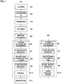
- a silicon wafer is produced through steps of slicing, chamfering, etching, mirror polishing, etching (clouding or roughening processing), pure water washing, neutralizing, pure water washing, drying and inspection. Below, the respective steps will be explained in detail.
- a silicon ingot grown by the CZ method is sliced to, for example, an 8-inch silicon wafer having a thickness of 860 ⁇ m or so in a slicing step in a step S1.
- edges of the sliced silicon wafer is chamfered to be a predetermined shape by a chamfering grind stone in a chamfering step in a step S2.
- edges of the silicon wafer are shaped to be rounded as prescribed (for example, a MOS type chamfered shape).
- the chamfered silicon wafer is wrapped by a wrapping step in a step S3.
- the silicon wafer is placed between a pair of wrapping boards being in parallel with each other, then, a mixture of alumina abrasive grains, and a dispersant and water is poured as a wrapping solution between the wrapping boards, and rotation and rubbing are performed under applying a pressure, so that both of the front and back surfaces of the wafer are mechanically wrapped.
- a wrapping amount of the silicon wafer is, for example, 30 to 80 ⁇ m or so for both of the back and front surfaces of the wafer.
- a step S4 the wrapped wafer after the wrapping is etched. Specifically, by immersing the silicon wafer in a mixed acid solution obtained by mixing fluorinated acid and nitric acid (from normal temperature to 50°C), etching of, for example, 20 ⁇ m for one surface and 40 ⁇ m or so for both surfaces is performed. As a result, distortion in the wrapping step and distortion in the chamfering step, etc. are removed.
- a mixed acid solution obtained by mixing fluorinated acid and nitric acid (from normal temperature to 50°C)
- both surfaces of the silicon wafer are mirror polished in a step S5.
- This step is performed by using a polishing apparatus having a rotating upper polishing board and a rotating lower polishing board arranged to face to each other.
- a polishing cloth is attached to each of the upper polishing board and the lower polishing board, and the silicon wafer is pressed against the upper and lower polishing cloth, so that the both surfaces are mirror polished at a time.
- a polishing allowance at this time is, for example, 10 ⁇ m.
- Predetermined slurry is supplied when performing the mirror polishing.
- the silicon wafer is taken out from the polishing apparatus and, in a step S6, clouding processing is performed by etching only the back surface of the wafer, wherein both surfaces are mirror finished.
- the alkali etchant according to the process of the present invention is used.
- the alkali etchant is for enabling easier identification of front and back with eyes by lowering a gloss level of the back surface of the wafer and has a characteristic of reducing gloss without deteriorating global flatness level of the back surface.
- a solution including sodium hydroxide NaOH as the main component wherein weight concentration (volume mole concentration) of sodium hydroxide is 55 wt% (22.3 mol/L) to 70 wt% (31.3 mol/L), may be selected.
- weight concentration of the sodium hydroxide is lower than 55 wt%, etching progresses, but reducing of the gloss is not observed and identification of front and back surfaces with eyes becomes impossible.
- an etchant including sodium hydroxide having weight concentration of exceeding 70 wt% is not suitable in terms of an etching processing temperature because it does not dissolve unless a temperature of the etchant is heightened to 100°C or so.
- a temperature of the etchant is set to 80°C to 90°C in the etching step in the step S6.
- a back surface of the wafer to be subjected to clouding processing is etched, for example, by 20 to 30 ⁇ m.
- a potassium hydroxide solution may be also used instead of the sodium hydroxide solution.
- a potassium hydroxide solution if a potassium hydroxide solution having a volume mole concentration in the same range as that of the volume mole concentration of the sodium hydroxide solution explained above is used, the same etching effect as that obtained by the sodium hydroxide solution is obtained. Note that when comparing a sodium hydroxide solution with a potassium hydroxide solution having the same volume mole concentration, the potassium hydroxide has a larger molecular weight, so that an absolute value in a weight concentration range also becomes large and it becomes harder to obtain a solution thereof. Accordingly, a sodium hydroxide solution is used as an alkali etchant according to the invention since the required solution can be easily made.
- the wafer is washed by immersing it in pure water or by spraying pure water thereon (pure water washing in a step S7), and neutralizing processing is performed for neutralizing the residual alkali etching solution on the wafer (a step S8).
- the neutralization processing the wafer is immersed in a fluorinated acid solution in a weight concentration of 10 wt% or lower at a normal temperature for 5 minutes. At this time, by adding ozone to the fluorinated acid solution, an oxidization film is formed on the wafer surface. Due to this, the silicon wafer surface is not exposed and it is possible to prevent contamination by metal impurities and adhesion of particles.
- the wafer attached with a fluorinated acid solution is washed by immersing it in pure water or spraying pure water thereon (pure water washing in the step S9) and, after that, spin drying, for example, at a rotation speed of 1500 rpm is performed for 120 seconds to dry the wafer (a step S10).
- wafer flatness level is inspected in a step S11.
- a flatness measurement device having a capacitance type distance sensor is used and, for example, wafers having GBIR(TTV) of 1.5 ⁇ m or less is determined to have a flatness level and those which do not satisfy that are determined to be defective in the flatness level.
- a fluorinated acid solution not added with ozone may be used in the neutralizing step and, for example, an ozone solution of 10ppm or more may be sprayed on the wafer immediately before the spin drying in a step S10'.
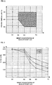
- FIG. 2 is a graph showing whether front and back can be identified or not in combinations of weight concentration of the alkali etchant and the etching (clouding processing) temperature: wherein a "o" mark in the graph indicates a point that identification is possible, while a " ⁇ " mark indicates a point that identification is not possible. Also, a hatched field in the figure indicates a range that identification is possible.
- FIG. 3 is a graph showing a gloss level (%) with respect to weight concentration (wt%) of the alkali etchant.
- Example 1 Weight Concentration of Sodium Hydroxide (wt%) Clouding Processing Temperature (°C) Lowering Rate of Gloss Level Before and After Clouding Processing Capability of Identifying Front and Back Example 1 70 90 81 ⁇ Example 2 70 85 70 ⁇ Example 3 70 80 55 ⁇ Example 4 60 90 70 ⁇ Example 5 60 85 55 ⁇ Example 6 60 80 40 ⁇ Example 7 55 90 50 ⁇ Example 8 55 85 40 ⁇ Comparative Example 1 50 90 15 ⁇ Comparative Example 2 50 85 5 ⁇ Comparative Example 3 50 80 0 ⁇ Comparative Example 4 40 90 0 ⁇ Comparative Example 5 40 85 0 ⁇ Comparative Example 6 40 80 0 ⁇ Comparative Example 7 55 80 31 ⁇
- a lowering rate of the gloss level has to be at least 40% or so for enabling to identify front and back of the mirror finished wafer with eyes, but it was confirmed that identifying of front and back of the mirror finished wafer with eyes becomes possible when the weight concentration of the alkali etchant is 60 wt% to 70 wt% and the etching temperature is 80°C to 90°C. Also, it was confirmed that when the weight concentration of the alkali etchant was 55 wt%, identifying of front and back of the mirror finished wafer with eyes becomes possible if the etching temperature is 85°C to 90°C.
- a slope has a relation of a minus linear function in a range that the etching temperature is 80 to 85°C when the weight concentration of the alkali etchant is 55 to 60 wt% as shown in FIG. 2 .
- Global flatness level GBIR(TTV) of a wafer before etching (clouding processing) and GBIR after the etching were respectively measured and a change rate thereof was also calculated.
- a thickness/flatness measurement apparatus made by Japan ADE Ltd. having a capacitance type distance sensor was used for measuring flatness level GBIR.
- the site flatness SFQR and nano-topography were measured.
Landscapes
- Engineering & Computer Science (AREA)
- Chemical & Material Sciences (AREA)
- General Physics & Mathematics (AREA)
- Physics & Mathematics (AREA)
- Condensed Matter Physics & Semiconductors (AREA)
- Manufacturing & Machinery (AREA)
- Computer Hardware Design (AREA)
- Microelectronics & Electronic Packaging (AREA)
- Power Engineering (AREA)
- General Chemical & Material Sciences (AREA)
- Chemical Kinetics & Catalysis (AREA)
- Materials Engineering (AREA)
- Organic Chemistry (AREA)
- Weting (AREA)
- Mechanical Treatment Of Semiconductor (AREA)
Claims (4)
- Procédé de production d'une tranche de silicium comprenant l'étape de gravage d'une surface principale d'une tranche de silicium polie miroir des deux côtés de façon à diminuer le niveau de brillance de ladite surface de silicium principale tout en maintenant un niveau de planéité globale, l'étape de gravage consistant à amener la surface principale en contact soit avec une solution d'hydroxyde de sodium conservée à une température de 80 °C à 90 °C et ayant une concentration en poids de 60 % en poids à 70 % en poids, soit avec une solution d'hydroxyde de sodium conservée à une température de 85 °C à 90 °C et ayant une concentration en poids de 55 % en poids à 60 % en poids.
- Procédé de production d'une tranche de silicium selon la revendication 1, comprenant en outre, après ladite étape de gravage, l'étape de rinçage de la tranche avec de l'eau pure, suivie de l'étape de neutralisation par une solution acide fluorée de la surface principale de la tranche mise en contact avec ledit agent de gravage.
- Procédé de production d'une tranche de silicium selon la revendication 2, dans lequel ladite solution acide contient de l'ozone.
- Procédé de production d'une tranche de silicium selon la revendication 2, dans lequel, après une étape supplémentaire de rinçage de la tranche avec de l'eau pure suivie de l'étape de neutralisation, une solution d'ozone de 10 ppm ou plus est pulvérisée sur la tranche immédiatement avant une étape d'essorage centrifuge.
Applications Claiming Priority (2)
| Application Number | Priority Date | Filing Date | Title |
|---|---|---|---|
| JP2004109870A JP4424039B2 (ja) | 2004-04-02 | 2004-04-02 | 半導体ウェーハの製造方法 |
| PCT/JP2005/005527 WO2005098921A1 (fr) | 2004-04-02 | 2005-03-25 | Réactif d'attaque alcalin pour contrôler la rugosité de surface d’une plaquette semi-conductrice |
Publications (3)
| Publication Number | Publication Date |
|---|---|
| EP1742256A1 EP1742256A1 (fr) | 2007-01-10 |
| EP1742256A4 EP1742256A4 (fr) | 2007-06-06 |
| EP1742256B1 true EP1742256B1 (fr) | 2018-08-15 |
Family
ID=35125357
Family Applications (1)
| Application Number | Title | Priority Date | Filing Date |
|---|---|---|---|
| EP05726977.1A Active EP1742256B1 (fr) | 2004-04-02 | 2005-03-25 | Agent de gravure alcalin pour le contrôle de la rugosité de surface d'une plaquette semi-conductrice |
Country Status (6)
| Country | Link |
|---|---|
| US (1) | US7851375B2 (fr) |
| EP (1) | EP1742256B1 (fr) |
| JP (1) | JP4424039B2 (fr) |
| KR (1) | KR100858774B1 (fr) |
| TW (1) | TW200539274A (fr) |
| WO (1) | WO2005098921A1 (fr) |
Families Citing this family (12)
| Publication number | Priority date | Publication date | Assignee | Title |
|---|---|---|---|---|
| JP4517867B2 (ja) * | 2005-01-31 | 2010-08-04 | 株式会社Sumco | シリコンウェーハ表面形状制御用エッチング液及び該エッチング液を用いたシリコンウェーハの製造方法 |
| US20080206992A1 (en) * | 2006-12-29 | 2008-08-28 | Siltron Inc. | Method for manufacturing high flatness silicon wafer |
| JP5261960B2 (ja) * | 2007-04-03 | 2013-08-14 | 株式会社Sumco | 半導体基板の製造方法 |
| JP2009004675A (ja) * | 2007-06-25 | 2009-01-08 | Shin Etsu Handotai Co Ltd | シリコンウエーハのエッチング方法及び装置 |
| DE102008014166B3 (de) * | 2008-03-14 | 2009-11-26 | Rena Gmbh | Verfahren zur Herstellung einer Siliziumoberfläche mit pyramidaler Textur |
| JP2009283616A (ja) * | 2008-05-21 | 2009-12-03 | Sumco Corp | 半導体ウェーハ |
| JP2009289877A (ja) * | 2008-05-28 | 2009-12-10 | Sumco Corp | 半導体ウェーハ |
| JP2009298680A (ja) * | 2008-06-17 | 2009-12-24 | Sumco Corp | 半導体ウェーハ |
| CN102356454B (zh) * | 2009-03-31 | 2014-03-26 | 栗田工业株式会社 | 蚀刻液的处理装置以及处理方法 |
| KR101024927B1 (ko) | 2009-07-30 | 2011-03-31 | 노바테크인더스트리 주식회사 | 에칭 공정에서의 세정 방법 |
| KR20120091371A (ko) * | 2010-02-26 | 2012-08-17 | 가부시키가이샤 사무코 | 반도체 웨이퍼의 제조 방법 |
| JP7023211B2 (ja) * | 2018-10-23 | 2022-02-21 | Sumco Techxiv株式会社 | ポリッシュドシリコンウェーハのエッチング条件調整方法及びそれを用いたポリッシュドシリコンウェーハの製造方法 |
Family Cites Families (23)
| Publication number | Priority date | Publication date | Assignee | Title |
|---|---|---|---|---|
| JPS4111011Y1 (fr) | 1964-10-20 | 1966-05-23 | ||
| JPS63221967A (ja) | 1987-03-10 | 1988-09-14 | Fujitsu Ltd | 研磨加工後のリンス方法 |
| JP2711389B2 (ja) | 1987-08-28 | 1998-02-10 | ユー,エス,フィルター/アローヘッド、インコーポレイテッド | 集積回路製作方法 |
| JPH02178919A (ja) * | 1988-12-29 | 1990-07-11 | Matsushita Electron Corp | シリコン基板への不純物拡散方法 |
| JP2830706B2 (ja) | 1993-07-24 | 1998-12-02 | 信越半導体株式会社 | シリコンウエーハのエッチング方法 |
| JP3678505B2 (ja) | 1995-08-29 | 2005-08-03 | 信越半導体株式会社 | 半導体ウェーハをエッチングするためのアルカリ溶液の純化方法及び半導体ウェーハのエッチング方法 |
| JP3522475B2 (ja) * | 1996-03-11 | 2004-04-26 | 三菱住友シリコン株式会社 | シリコンウェーハ表面粗さ制御用のエッチャント |
| JPH09270396A (ja) | 1996-03-29 | 1997-10-14 | Komatsu Electron Metals Co Ltd | 半導体ウェハの製法 |
| JP3658454B2 (ja) | 1996-03-29 | 2005-06-08 | コマツ電子金属株式会社 | 半導体ウェハの製造方法 |
| JP3686910B2 (ja) * | 1997-09-29 | 2005-08-24 | 三菱住友シリコン株式会社 | シリコンウェーハのエッチング方法 |
| MY119304A (en) | 1997-12-11 | 2005-04-30 | Shinetsu Handotai Kk | Silicon wafer etching method and silicon wafer etchant |
| DE19953152C1 (de) | 1999-11-04 | 2001-02-15 | Wacker Siltronic Halbleitermat | Verfahren zur naßchemischen Oberflächenbehandlung einer Halbleiterscheibe |
| JP3943869B2 (ja) | 2000-06-29 | 2007-07-11 | 信越半導体株式会社 | 半導体ウエーハの加工方法および半導体ウエーハ |
| GB2368971B (en) | 2000-11-11 | 2005-01-05 | Pure Wafer Ltd | Process for Reclaimimg Wafer Substrates |
| JP3413726B2 (ja) * | 2000-12-28 | 2003-06-09 | 株式会社スーパーシリコン研究所 | ウエハ洗浄方法 |
| JP2003007672A (ja) | 2001-06-25 | 2003-01-10 | Toshiba Ceramics Co Ltd | シリコン半導体ウェーハのエッチング方法 |
| JP2003229392A (ja) * | 2001-11-28 | 2003-08-15 | Shin Etsu Handotai Co Ltd | シリコンウエーハの製造方法及びシリコンウエーハ並びにsoiウエーハ |
| JP3890981B2 (ja) * | 2002-01-07 | 2007-03-07 | 株式会社Sumco | アルカリエッチング液及びこのエッチング液を用いたシリコンウェーハのエッチング方法並びにこの方法を用いたシリコンウェーハの表裏面差別化方法 |
| TW200411759A (en) * | 2002-09-18 | 2004-07-01 | Memc Electronic Materials | Process for etching silicon wafers |
| JP4426192B2 (ja) | 2003-02-14 | 2010-03-03 | ニッタ・ハース株式会社 | 研磨用組成物の製造方法 |
| JPWO2005055302A1 (ja) | 2003-12-05 | 2007-06-28 | 株式会社Sumco | 片面鏡面ウェーハの製造方法 |
| KR20050065312A (ko) * | 2003-12-25 | 2005-06-29 | 마츠시타 덴끼 산교 가부시키가이샤 | 반도체웨이퍼의 세정방법 |
| JP4517867B2 (ja) | 2005-01-31 | 2010-08-04 | 株式会社Sumco | シリコンウェーハ表面形状制御用エッチング液及び該エッチング液を用いたシリコンウェーハの製造方法 |
-
2004
- 2004-04-02 JP JP2004109870A patent/JP4424039B2/ja not_active Expired - Lifetime
-
2005
- 2005-03-25 WO PCT/JP2005/005527 patent/WO2005098921A1/fr active Application Filing
- 2005-03-25 EP EP05726977.1A patent/EP1742256B1/fr active Active
- 2005-03-25 KR KR1020067022989A patent/KR100858774B1/ko active IP Right Grant
- 2005-03-25 US US10/599,576 patent/US7851375B2/en active Active
- 2005-03-31 TW TW094110355A patent/TW200539274A/zh unknown
Non-Patent Citations (1)
| Title |
|---|
| None * |
Also Published As
| Publication number | Publication date |
|---|---|
| JP2005294682A (ja) | 2005-10-20 |
| WO2005098921A1 (fr) | 2005-10-20 |
| EP1742256A4 (fr) | 2007-06-06 |
| KR20060133082A (ko) | 2006-12-22 |
| US20070298618A1 (en) | 2007-12-27 |
| TW200539274A (en) | 2005-12-01 |
| EP1742256A1 (fr) | 2007-01-10 |
| US7851375B2 (en) | 2010-12-14 |
| TWI292586B (fr) | 2008-01-11 |
| KR100858774B1 (ko) | 2008-09-16 |
| JP4424039B2 (ja) | 2010-03-03 |
Similar Documents
| Publication | Publication Date | Title |
|---|---|---|
| EP1742256B1 (fr) | Agent de gravure alcalin pour le contrôle de la rugosité de surface d'une plaquette semi-conductrice | |
| US7829467B2 (en) | Method for producing a polished semiconductor | |
| US6482749B1 (en) | Method for etching a wafer edge using a potassium-based chemical oxidizer in the presence of hydrofluoric acid | |
| KR100792774B1 (ko) | 반도체 웨이퍼의 가공방법 및 반도체 웨이퍼 | |
| EP2260507B1 (fr) | Procédés pour graver le bord d'une tranche de silicium, tranche de silicium, appareil de gravure | |
| JP3004891B2 (ja) | 表面粗さを減少させるための半導体ウエハの粗研磨法 | |
| EP3605590B1 (fr) | Composition de solution de nettoyage | |
| US6376335B1 (en) | Semiconductor wafer manufacturing process | |
| KR20000017512A (ko) | 웨이퍼 기판 재생방법 및 웨이퍼 기판 재생을 위한 연마액 조성물 | |
| EP1693887A1 (fr) | Procede de traitement de plaquette au silicium | |
| JP3066750B2 (ja) | 半導体ウェーハの製造方法 | |
| JP3943869B2 (ja) | 半導体ウエーハの加工方法および半導体ウエーハ | |
| WO2001049450A1 (fr) | Procede de polissage chimico-mecanique pour la fabrication de plaquettes de silicium sans striations dues au dopant | |
| EP0813931B1 (fr) | Procédé pour la fabrication de tranches de semi-conducteur | |
| US5904568A (en) | Method of manufacturing a semiconductor wafer | |
| TWI515782B (zh) | Silicon wafer grinding method and abrasive | |
| JP3906688B2 (ja) | 半導体ウエーハ用研磨布及び研磨方法 | |
| US20240203745A1 (en) | Silicon wafer manufacturing method | |
| KR20110036990A (ko) | 균일 산화막 형성 방법 및 세정 방법 | |
| JP3651440B2 (ja) | シリコンウェーハの評価方法及びそのエッチング液 | |
| JP3551300B2 (ja) | 高平坦度ウェーハの製造方法 | |
| US20020175143A1 (en) | Processes for polishing wafers | |
| JP2007150196A (ja) | 半導体ウエーハの洗浄方法および製造方法 | |
| WO2014055752A1 (fr) | Traitement par ultraviolets de tranches polies | |
| WO2001034877A1 (fr) | Solution alcaline de gravure et procede permettant de graver des plaquettes de semi-conducteurs |
Legal Events
| Date | Code | Title | Description |
|---|---|---|---|
| PUAI | Public reference made under article 153(3) epc to a published international application that has entered the european phase |
Free format text: ORIGINAL CODE: 0009012 |
|
| 17P | Request for examination filed |
Effective date: 20061031 |
|
| AK | Designated contracting states |
Kind code of ref document: A1 Designated state(s): DE |
|
| RIN1 | Information on inventor provided before grant (corrected) |
Inventor name: TAKAISHI, KAZUSHIGE,C/O SUMCO CORPORATION Inventor name: KOYATA, SAKAE,C/O SUMCO CORPORATION |
|
| A4 | Supplementary search report drawn up and despatched |
Effective date: 20070508 |
|
| RIC1 | Information provided on ipc code assigned before grant |
Ipc: H01L 21/306 20060101AFI20061117BHEP |
|
| DAX | Request for extension of the european patent (deleted) | ||
| RBV | Designated contracting states (corrected) |
Designated state(s): DE |
|
| 17Q | First examination report despatched |
Effective date: 20070824 |
|
| GRAP | Despatch of communication of intention to grant a patent |
Free format text: ORIGINAL CODE: EPIDOSNIGR1 |
|
| RIC1 | Information provided on ipc code assigned before grant |
Ipc: H01L 21/02 20060101ALI20180301BHEP Ipc: H01L 21/306 20060101AFI20180301BHEP Ipc: C09K 13/02 20060101ALI20180301BHEP |
|
| INTG | Intention to grant announced |
Effective date: 20180315 |
|
| RAP1 | Party data changed (applicant data changed or rights of an application transferred) |
Owner name: SUMCO CORPORATION |
|
| RIN1 | Information on inventor provided before grant (corrected) |
Inventor name: TAKAISHI, KAZUSHIGE Inventor name: KOYATA, SAKAE |
|
| GRAS | Grant fee paid |
Free format text: ORIGINAL CODE: EPIDOSNIGR3 |
|
| GRAA | (expected) grant |
Free format text: ORIGINAL CODE: 0009210 |
|
| AK | Designated contracting states |
Kind code of ref document: B1 Designated state(s): DE |
|
| REG | Reference to a national code |
Ref country code: DE Ref legal event code: R096 Ref document number: 602005054418 Country of ref document: DE |
|
| REG | Reference to a national code |
Ref country code: DE Ref legal event code: R097 Ref document number: 602005054418 Country of ref document: DE |
|
| PLBE | No opposition filed within time limit |
Free format text: ORIGINAL CODE: 0009261 |
|
| STAA | Information on the status of an ep patent application or granted ep patent |
Free format text: STATUS: NO OPPOSITION FILED WITHIN TIME LIMIT |
|
| 26N | No opposition filed |
Effective date: 20190516 |
|
| PGFP | Annual fee paid to national office [announced via postgrant information from national office to epo] |
Ref country code: DE Payment date: 20240320 Year of fee payment: 20 |