EP1686628A2 - Bildaufnahmesensorverpackung und ihr Herstellungsverfahren - Google Patents
Bildaufnahmesensorverpackung und ihr Herstellungsverfahren Download PDFInfo
- Publication number
- EP1686628A2 EP1686628A2 EP05257576A EP05257576A EP1686628A2 EP 1686628 A2 EP1686628 A2 EP 1686628A2 EP 05257576 A EP05257576 A EP 05257576A EP 05257576 A EP05257576 A EP 05257576A EP 1686628 A2 EP1686628 A2 EP 1686628A2
- Authority
- EP
- European Patent Office
- Prior art keywords
- image sensor
- sensor module
- chip scale
- scale image
- glass
- Prior art date
- Legal status (The legal status is an assumption and is not a legal conclusion. Google has not performed a legal analysis and makes no representation as to the accuracy of the status listed.)
- Withdrawn
Links
Images


Classifications
-
- H—ELECTRICITY
- H10—SEMICONDUCTOR DEVICES; ELECTRIC SOLID-STATE DEVICES NOT OTHERWISE PROVIDED FOR
- H10F—INORGANIC SEMICONDUCTOR DEVICES SENSITIVE TO INFRARED RADIATION, LIGHT, ELECTROMAGNETIC RADIATION OF SHORTER WAVELENGTH OR CORPUSCULAR RADIATION
- H10F39/00—Integrated devices, or assemblies of multiple devices, comprising at least one element covered by group H10F30/00, e.g. radiation detectors comprising photodiode arrays
- H10F39/80—Constructional details of image sensors
- H10F39/806—Optical elements or arrangements associated with the image sensors
-
- H—ELECTRICITY
- H10—SEMICONDUCTOR DEVICES; ELECTRIC SOLID-STATE DEVICES NOT OTHERWISE PROVIDED FOR
- H10F—INORGANIC SEMICONDUCTOR DEVICES SENSITIVE TO INFRARED RADIATION, LIGHT, ELECTROMAGNETIC RADIATION OF SHORTER WAVELENGTH OR CORPUSCULAR RADIATION
- H10F39/00—Integrated devices, or assemblies of multiple devices, comprising at least one element covered by group H10F30/00, e.g. radiation detectors comprising photodiode arrays
- H10F39/10—Integrated devices
- H10F39/12—Image sensors
-
- H—ELECTRICITY
- H04—ELECTRIC COMMUNICATION TECHNIQUE
- H04N—PICTORIAL COMMUNICATION, e.g. TELEVISION
- H04N23/00—Cameras or camera modules comprising electronic image sensors; Control thereof
- H04N23/57—Mechanical or electrical details of cameras or camera modules specially adapted for being embedded in other devices
-
- H—ELECTRICITY
- H10—SEMICONDUCTOR DEVICES; ELECTRIC SOLID-STATE DEVICES NOT OTHERWISE PROVIDED FOR
- H10F—INORGANIC SEMICONDUCTOR DEVICES SENSITIVE TO INFRARED RADIATION, LIGHT, ELECTROMAGNETIC RADIATION OF SHORTER WAVELENGTH OR CORPUSCULAR RADIATION
- H10F39/00—Integrated devices, or assemblies of multiple devices, comprising at least one element covered by group H10F30/00, e.g. radiation detectors comprising photodiode arrays
- H10F39/011—Manufacture or treatment of image sensors covered by group H10F39/12
-
- H—ELECTRICITY
- H10—SEMICONDUCTOR DEVICES; ELECTRIC SOLID-STATE DEVICES NOT OTHERWISE PROVIDED FOR
- H10F—INORGANIC SEMICONDUCTOR DEVICES SENSITIVE TO INFRARED RADIATION, LIGHT, ELECTROMAGNETIC RADIATION OF SHORTER WAVELENGTH OR CORPUSCULAR RADIATION
- H10F39/00—Integrated devices, or assemblies of multiple devices, comprising at least one element covered by group H10F30/00, e.g. radiation detectors comprising photodiode arrays
- H10F39/80—Constructional details of image sensors
- H10F39/804—Containers or encapsulations
-
- H—ELECTRICITY
- H10—SEMICONDUCTOR DEVICES; ELECTRIC SOLID-STATE DEVICES NOT OTHERWISE PROVIDED FOR
- H10F—INORGANIC SEMICONDUCTOR DEVICES SENSITIVE TO INFRARED RADIATION, LIGHT, ELECTROMAGNETIC RADIATION OF SHORTER WAVELENGTH OR CORPUSCULAR RADIATION
- H10F77/00—Constructional details of devices covered by this subclass
- H10F77/40—Optical elements or arrangements
- H10F77/407—Optical elements or arrangements indirectly associated with the devices
-
- H—ELECTRICITY
- H10—SEMICONDUCTOR DEVICES; ELECTRIC SOLID-STATE DEVICES NOT OTHERWISE PROVIDED FOR
- H10F—INORGANIC SEMICONDUCTOR DEVICES SENSITIVE TO INFRARED RADIATION, LIGHT, ELECTROMAGNETIC RADIATION OF SHORTER WAVELENGTH OR CORPUSCULAR RADIATION
- H10F77/00—Constructional details of devices covered by this subclass
- H10F77/50—Encapsulations or containers
-
- H—ELECTRICITY
- H10—SEMICONDUCTOR DEVICES; ELECTRIC SOLID-STATE DEVICES NOT OTHERWISE PROVIDED FOR
- H10W—GENERIC PACKAGES, INTERCONNECTIONS, CONNECTORS OR OTHER CONSTRUCTIONAL DETAILS OF DEVICES COVERED BY CLASS H10
- H10W72/00—Interconnections or connectors in packages
-
- H—ELECTRICITY
- H10—SEMICONDUCTOR DEVICES; ELECTRIC SOLID-STATE DEVICES NOT OTHERWISE PROVIDED FOR
- H10W—GENERIC PACKAGES, INTERCONNECTIONS, CONNECTORS OR OTHER CONSTRUCTIONAL DETAILS OF DEVICES COVERED BY CLASS H10
- H10W72/00—Interconnections or connectors in packages
- H10W72/071—Connecting or disconnecting
- H10W72/072—Connecting or disconnecting of bump connectors
- H10W72/07251—Connecting or disconnecting of bump connectors characterised by changes in properties of the bump connectors during connecting
-
- H—ELECTRICITY
- H10—SEMICONDUCTOR DEVICES; ELECTRIC SOLID-STATE DEVICES NOT OTHERWISE PROVIDED FOR
- H10W—GENERIC PACKAGES, INTERCONNECTIONS, CONNECTORS OR OTHER CONSTRUCTIONAL DETAILS OF DEVICES COVERED BY CLASS H10
- H10W72/00—Interconnections or connectors in packages
- H10W72/20—Bump connectors, e.g. solder bumps or copper pillars; Dummy bumps; Thermal bumps
-
- H—ELECTRICITY
- H10—SEMICONDUCTOR DEVICES; ELECTRIC SOLID-STATE DEVICES NOT OTHERWISE PROVIDED FOR
- H10W—GENERIC PACKAGES, INTERCONNECTIONS, CONNECTORS OR OTHER CONSTRUCTIONAL DETAILS OF DEVICES COVERED BY CLASS H10
- H10W72/00—Interconnections or connectors in packages
- H10W72/90—Bond pads, in general
- H10W72/921—Structures or relative sizes of bond pads
- H10W72/922—Bond pads being integral with underlying chip-level interconnections
-
- H—ELECTRICITY
- H10—SEMICONDUCTOR DEVICES; ELECTRIC SOLID-STATE DEVICES NOT OTHERWISE PROVIDED FOR
- H10W—GENERIC PACKAGES, INTERCONNECTIONS, CONNECTORS OR OTHER CONSTRUCTIONAL DETAILS OF DEVICES COVERED BY CLASS H10
- H10W72/00—Interconnections or connectors in packages
- H10W72/90—Bond pads, in general
- H10W72/921—Structures or relative sizes of bond pads
- H10W72/923—Bond pads having multiple stacked layers
-
- H—ELECTRICITY
- H10—SEMICONDUCTOR DEVICES; ELECTRIC SOLID-STATE DEVICES NOT OTHERWISE PROVIDED FOR
- H10W—GENERIC PACKAGES, INTERCONNECTIONS, CONNECTORS OR OTHER CONSTRUCTIONAL DETAILS OF DEVICES COVERED BY CLASS H10
- H10W72/00—Interconnections or connectors in packages
- H10W72/90—Bond pads, in general
- H10W72/941—Dispositions of bond pads
- H10W72/9415—Dispositions of bond pads relative to the surface, e.g. recessed, protruding
-
- H—ELECTRICITY
- H10—SEMICONDUCTOR DEVICES; ELECTRIC SOLID-STATE DEVICES NOT OTHERWISE PROVIDED FOR
- H10W—GENERIC PACKAGES, INTERCONNECTIONS, CONNECTORS OR OTHER CONSTRUCTIONAL DETAILS OF DEVICES COVERED BY CLASS H10
- H10W90/00—Package configurations
- H10W90/701—Package configurations characterised by the relative positions of pads or connectors relative to package parts
- H10W90/721—Package configurations characterised by the relative positions of pads or connectors relative to package parts of bump connectors
- H10W90/724—Package configurations characterised by the relative positions of pads or connectors relative to package parts of bump connectors between a chip and a stacked insulating package substrate, interposer or RDL
Definitions
- the present invention relates to a chip scale image sensor module used in digital optical devices and the fabrication method of the same. More particularly, the present invention relates to a chip scale image sensor module and the fabrication method of the same which minimizes the size of an image sensor referred to as a complementary metal oxide semiconductor (CMOS) or a charge coupled device (CCD), capable of screening and using good quality image sensors to fabricate good quality packages, thereby saving the manufacturing costs and having an advantage in mass production.
- CMOS complementary metal oxide semiconductor
- CCD charge coupled device
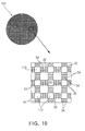
- FIG. 1 illustrates a front side of an image sensor module 300 according to the prior art.
- the image sensor module 300 is of a basic structure which can be applied to a camera module of a mobile phone in the following three forms: Chip on Board (COB) using gold wire bonding technique, Chip on FPC (COF) using Anisotropic Conductive Film (ACF) or Non-conductive Paste (NCP), and Chip Scale Package (CSP).
- COB Chip on Board
- COF Chip on FPC
- ACF Anisotropic Conductive Film
- NCP Non-conductive Paste
- CSP Chip Scale Package
- FIG. 1 illustrates the chip scale image sensor module 300 produced by the conventional Shell-OPC, which is published in PCT application WO 99/40624.
- This conventional chip scale image sensor module 300 having a thin, dense structure, is well-protected from outside environment, mechanically strengthened, and plated with a plurality of electrical contacts 312 along edge surfaces 314.
- the contacts 312 extend over the entire edge surfaces 314 onto a planar surface 316 of the image sensor module. With this arrangement of the contacts, the image sensor module 300 and the edge can be attached by the planar surface to the circuit board.
- the above described conventional image sensor module 300 includes fusible bumps 317 disposed at the end of each contact 312. These fusible bumps 317 are arranged in an array.
- FIG. 2 illustrates another conventional chip scale image sensor module 350 similar to the above description, which is published in PCT application WO 99/40624.
- This conventional chip scale image sensor module 350 has a light emitter and/or light receiver, with the upper and lower surfaces formed of electric insulation and mechanical protective material. At least one of the upper and lower surfaces includes an integrated circuit die 372 having a protective film 357 transmitting light, and pads are mounted on electrically insulated edge surfaces 364.
- the conventional chip scale image sensor module 350 has a structure in which a plurality of electric contacts 382 are plated along the edge surfaces 364, and screening filter and/or reflection prevention coating film 395 is formed on the outer contact surface 356 of a transparent protective film 357.
- FIG. 3 illustrates another conventional chip scale image sensor module 400, which is published in PCT application WO 01/43181.
- This conventional chip scale image sensor module 400 has a micro-lens array 410 formed on a crystalline silicon substrate. Underlying the silicon substrate 412, a package layer 416 formed typically of glass is sealed with epoxy 414. Along the edges of the package layer 416, electric contacts 428, which typically form bumps 430 thereon, are formed. Also, conductive pads 432 connect the silicon substrate 412 with the electric contacts 428.
- a glass layer 444 and spacer elements 436 related thereto are sealed by an adhesive such as epoxy 438 in the upper part of the silicon substrate 412 to form a space 446 between the micro-lens array 410 and the glass layer 444.
- the package layer 444 is preferably transparent.
- FIG. 4 illustrates a chip scale image sensor module 450 of a different type from the above described ones, published in Japanese Patent Application No. 2002-274807.
- This conventional chip scale image sensor module 450 has a transparent adhesive layer 458 attached to a glass substrate 459 corresponding to a plurality of image sensor modules.
- silicon substrates 451 having photoelectric device regions 452 are attached at a regular interval.
- connecting wires 457 are connected to connection pads 453 of the silicon substrate 451 near the bottom surface of the silicon substrate 451.
- FIG. 5 illustrates another conventional chip scale image sensor module 500, which is published in Japanese Laid-open Patent Application No. 2004-153260.
- This conventional chip scale image sensor module 500 has pad electrode 511 formed on the semiconductor tip 510, and supporting substrate 513 attached to the surface of the semiconductor tip 510. Also, vias 517 extend from the bottom surface of the semiconductor tip 510 to reach the surface of the pad electrode 511, and inside each via 517, columnar terminal 520 is formed, connected to the pad electrode 511.
- the columnar terminal 520 forms rerouting pad layer 521, with solder masks 522 coated thereon, and bumps 523 thereon electrically connected to the rerouting pad layer 521.
- the prior art described above is aimed to provide a chip scale image sensor module with highly reliable Ball Grid Array (BGA), whose unique structure is capable of preventing disconnection or deterioration of step coverage.
- BGA Ball Grid Array
- the conventional image sensor modules are faced with a problem when the yield of the image sensors is particularly low.
- the problem occurs due to the fact that defective image sensors are also packaged in the manufacturing process, resulting in the packaging costs of good quality image sensors burdened with the packaging costs of defective image sensors, which in turn, increases the costs of production.
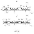
- FIG. 6 (a) and (b) illustrate another conventional chip scale image sensor module 600, which uses glass for glass substrate 605 having metal wires 610 and insulation films 612 protecting the metal wires 610 thereon. Also, image sensor chips 620 are electrically connected to the glass substrate 605 using solder ball joints 630.
- outer solder balls 640 are formed on the metal wires 610 to be electrically connected to the outside PCB substrate (not shown).
- the electric signals from the image sensor chips 620 are transmitted to the outside PCB substrate via the metal wires 610 and the outer solder balls 640 on the glass substrate 605.
- the above described conventional chip scale image sensor modules receive light whose wavelength not only includes infrared ray region, visible ray region, ultraviolet ray region, and other regions, but also includes a visible ray region of the wavelength in which humans see and perceive objects.
- each of the camera modules installed with the above described conventional image sensor modules has an optical filter. If the optical filter is an IR filter, it can lower transmission rate of the infrared rays.
- the optical filter lowers the transmission rate of the infrared rays while increasing reflection rate to protect the image sensor receiving the light, and also increasing the transmission rate of the visible ray region perceived by humans.
- the optical filter is coated on a rectangular glass and cut into individual units which are then attached to each image sensor module. Therefore, in the prior art, the installation of the optical filter was conducted separately from the installation of the image sensor module, requiring so many steps in the manufacturing process.
- the present invention has been made to solve the foregoing problems of the prior art and it is therefore an object of the present invention to provide a chip scale image sensor module and the fabrication method of the same which enables packaging only the good quality image sensors, tremendously increasing the yield of the image sensor module, thereby saving the manufacturing costs and having an advantage in mass production.
- the invention provides a chip scale image sensor module used in digital devices including: an optical filter removing specific wavelength from the light incident onto the image sensor; a glass layer attached to the optical filter to protect the coating layer, with pad electrodes formed on the backside thereof; an image sensor attached to the pad electrodes of the glass layer, with redistribution pads formed from the pad electrodes to the backside thereof; and solder balls provided on the backside of the image sensor, electrically connected to the pad electrodes.
- the present invention provides a fabrication method of a chip scale image sensor module used in digital devices, the method including steps of: forming a glass wafer by attaching a wafer-type glass layer to a wafer-type optical filter removing specific wavelength from the light incident onto the image sensor; forming pad electrodes on the glass layer of the glass wafer; bonding the pad electrodes with bumps to attach a plurality of image sensors on the glass wafer; forming redistribution pads connected to the pad electrodes of the glass wafer in the backside of each image sensor; providing solder balls on each redistribution pad of the image sensor; and dicing the glass wafer into a plurality of image sensor modules.
- FIG. 1 is a block diagram illustrating a chip scale image sensor module according to the prior art in which: (a) is a front side view, (b) is a rear side view, and (c) is a perspective view with solder balls;
- FIG. 2 is a longitudinal sectional view illustrating another structure of the chip scale image sensor module according to the prior art
- FIG. 3 is a longitudinal sectional view illustrating another structure of the chip scale image sensor module according to the prior art
- FIG. 4 is a longitudinal sectional view illustrating another chip scale image sensor module having solder balls according to the prior art
- FIG. 5 is a longitudinal sectional view illustrating another chip scale sensor module having vias
- FIG. 6 (a) and (b) are longitudinal sectional views illustrating another chip scale image sensor module according to the prior art
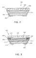
- FIG. 7 is a sectional view illustrating a chip scale image sensor module according to the present invention.
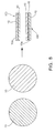
- FIG. 8 is a view illustrating the process of forming a glass wafer by binding the glass layer with the optical filter in the fabrication method of the chip scale image sensor module according to the present invention
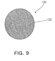
- FIG. 9 is a view illustrating the process of forming metal layer on the glass wafer in the fabrication method of the chip scale image sensor module according to the present invention.
- FIG. 10 is a view illustrating the process of forming pad electrodes on the metal layer of the glass wafer in the fabrication method of the chip scale image sensor module according to the present invention.
- FIG. 11 is a view illustrating the process of attaching the image sensor to the pad electrodes on the glass wafer in the fabrication method of the chip scale image sensor module according to the present invention
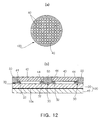
- FIG. 12 is a view illustrating the process of forming resin layers between the image sensors on the glass wafer in the fabrication method of the chip scale image sensor module according to the present invention.
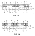
- FIG. 13 is a view illustrating the process of forming vias in the resin layers on the glass wafer in the fabrication method of the chip scale image sensor module according to the present invention
- FIG. 14 is a view illustrating the process of forming redistribution pads through the vias in the resin layers in the fabrication method of the chip scale image sensor module according to the present invention.
- FIG. 15 is a view illustrating the process of providing solder balls on the redistribution pads in the fabrication method of the chip scale image sensor module according to the present invention.
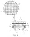
- FIG. 16 is a view illustrating the process of dicing the glass wafer obtained from the fabrication method of the scale chip image sensor module into a plurality of chip scale image sensor modules, according to the present invention.
- the image sensor module 1 integrally includes an optical filter 10 which removes specific wavelength from the light incident onto the image sensor.
- the optical filter 10 may be, but not limited to, a general IR filter.
- the optical filter 10 may have its coating layer 10a on both upper and lower surfaces, but preferably, the coating layer 10a is formed to face the glass layer 20.
- the image sensor module 1 of the present invention has a glass layer 20 attached to the optical filter 10 to protect the coating layer 10a, with pad electrodes 30 formed on the backside thereof.
- the glass layer 20 may be formed by adhesively attaching the optical filter 10 with a transparent adhesive or by conducting a fusion bonding of H and OH groups using the moisture in the air.
- the latter fusion bonding guarantees 100% of transmission rate of light since the glass layer 20 and the optical filter 10 can be bonded with nothing in between. Therefore, superior transmission characteristics of light can be obtained with fusion boding to using a transparent adhesive.
- the coating layer 10a of the optical filter is formed between the optical filter 10 and the glass layer 20.
- the glass layer 20 has pad electrodes 30 formed on its outer surface thereof.
- the seed metal of the pad electrodes 30 may include TiW, Al, Cu and Ni when using PVD sputtering, and also may include Pd when using electroless plating.
- a main metal part of the pad electrodes 30 on the seed metal is generally Au/Ni, Au on Ni, and also includes plating of Cu, Sn and alloys of Sn.
- the pad electrodes 30 are obtained from patterning the metal coated on the glass layer 20.
- the resultant pad electrodes 30 includes flip-chip pads which are flip-chip bonded to the image sensor 40 described hereinbelow, and expansion pads 34 for redistribution.
- the chip scale image sensor module 1 includes an image sensor 40 which is attached to the pad electrodes 30 of the glass layer 20, with redistribution pads 42 formed from the pad electrodes 30 to the backside of the image sensor 40.
- the flip-chip bonded image sensors 40 are only the ones with good quality.
- the flip-chip image sensor 40 is provided with Au bumps 44, and bonded with Anisotropic Conductive Film (ACF) .
- the ACF may be substituted with Anisotropic Conductive Paste (ACP), Non-Conductive Paste (NCP) and Non-Conductive Film (NCF).
- the bumps 44 of the image sensor 40 may include solder ball bumps rather than Au bumps.
- the chip scale image sensor module 1 includes redistribution pads 42 formed in the backside of the image sensor 40, electrically connected to the expansion pads 34 of the pad electrodes 30 formed on the glass layer 20. Further, the image sensor module 1 includes insular resin layer 50 formed between the expansion pads 34 and the redistribution pads 42, and vias 52 perforated through the resin layer 50. The vias 52 are plated with metal to have the expansion pads 34 electrically connected to the redistribution pads 42.
- the present invention includes solder balls 70 provided on the backside of the image sensor 40, and electrically connected to the pad electrodes 30.
- the chip scale image sensor module 1 can solve the foregoing problems with conventional methods. That is, in the conventional method, when the image sensor is completed into a wafer form, a low yield of image sensor wafers including a great number of defective image sensors is manufactured to constitute the image sensor modules, resulting in defective image sensor modules. As a result, the defective image sensor modules are discarded and the costs incurred thereby are entirely burdened on the manufacturing costs of the good quality image sensor modules.
- the fabrication method of the chip scale image sensor module starts with the step of attaching the wafer-type glass layer 20 to the wafer-type optical filter 10 which removes specific wavelength from the light incident onto the image sensor 40 to form a glass wafer 100.
- glass is processed into a wafer-type to form a glass layer 20 while an optical filter coating layer 10a is formed on the other wafer-type glass to form a wafer-type optical filter 10, and then the two are bonded to form a glass wafer 100.
- a coating layer is formed on a rectangular glass, cut into individual optical filters, which are then attached to the camera modules.
- the present invention provides the optical filter 10 in a wafer form, producing a glass wafer 100. Then, the resultant glass wafer 100 is packaged with the fabrication steps at a wafer level, diced into individual parts having an image sensor 40 to obtain a plurality of chip scale image sensor modules 1.
- the step of forming the glass wafer 100 includes attaching the wafer-type glass layer 20 and the wafer-type optical filter 10, which may be conducted using a transparent adhesive 16, as shown in FIG. 8, and also via fusion bonding of H and OH groups using the moisture in the air.
- the latter fusion bonding allows bonding with nothing in between the glass layer 20 and the optical filter 10, guaranteeing 100% of light transmission rate. Therefore, better light transmission characteristics can be obtained with fusion bonding than with the transparent adhesive 16.
- the glass layer 20 and the wafer-type optical filter 10 are attached to each other to form a glass wafer 100.
- the fabrication method of the chip scale image sensor module includes forming pad electrodes 30 on the glass layer 20 of the glass wafer 100.
- This step includes covering the glass wafer 100 with metal to form a pattern thereon.
- the step of forming metal 102 on the glass layer 20 of the glass wafer 100 includes covering the glass layer 20 with seed metal and then covering with main metal.
- the seed metal may include TiW, Al, Cu, and Ni when using sputtering of PVD. Pd may be used in electroless plating.
- a main metal part on the seed metal generally includes Au/Ni, Au on Ni, and also may include plating of Cu, Sn and alloys of Sn.
- the plating method may adopt PVD sputtering, as with seed metal, but electric plating is more appropriate in terms of mass production.
- the step of forming pad electrodes 30 on the glass layer 20 of the glass wafer 100 includes patterning the metal coated on the glass layer 20 of the glass wafer 100. As shown in FIG. 10, this patterning step includes forming a pattern on the metal 102 formed on the glass layer 20 to form flip-chip pads which is to be flip-chip bonded with the image sensor 40 so as to mount the image sensor 40. This patterning step further includes forming expansion pads 34 for forming redistribution pads 42 described hereinbelow.
- image sensor regions 110 are formed, with flip-chip pads 32 and expansion pads 34 surrounding the image sensor regions 110.
- the fabrication method of the chip scale image sensor module according to the present invention includes bonding the bumps 44 with the pad electrodes 30 to attach a plurality of image sensors 40 on the glass wafer 100.
- This step involves flip-chip bonding only the good quality image sensors to the glass wafer 100. As shown in FIG. 11, this step bonds the bumps 44 formed on the good quality image sensors 40 with the flip-chip pads 32 of the glass wafer 100 formed in advance.
- the flip-chip image sensor 40 is provided with Au bumps 44, and bonded with ACF.
- the present invention is not limited to the above, and the ACF may be substituted with ACP, NCP and NCF.
- the bumps 44 of the image sensor 40 may be substituted with solder ball bumps.
- the present invention is able to remove defective image sensors 40 while screening and mounting only good quality image sensors 40, obtaining good quality chip scale image sensor modules 1.
- the fabrication method of the chip scale image sensor module according to the present invention includes forming redistribution pads 42 on the backside of the image sensor 40 connected to the pad electrodes 30 of the glass wafer 100.
- this step of forming redistribution pads 42 includes filling with resin layer 50 the space between the image sensors 40 flip-chip bonded on the glass wafer 100.
- the space between the image sensors 40 is filled with resin, and then the resultant structure is baked to be hardened.
- the resin includes epoxy, Benzocyclobutene (BCB), etc.
- the above step includes etching the vias 52 in the hardened resin.
- etching the vias 52 There may be several methods for etching the vias 52.
- the vias 52 can be etched in a photolithography step using a mask, including exposure to light and development.
- the vias 52 can also be etched by laser or dry etching.
- the above step includes coating or filling with metal inside the vias 52 formed in the hardened resin layer 50 to form redistribution pads 42 on the backside of the image sensor 40 to be electrically connected to the expansion pads 34.
- this step extends the expansion pads 34 to the backside of the image sensor 40 to form the redistribution pads 42.
- This can be conducted by forming the seed metal via PVD, Chemical Vapor Deposition (CVD) or electroless method, then by coating or filling with metal inside the vias 52 by means of PVD, electric plating, conducting material, etc.
- CVD Chemical Vapor Deposition
- etching the resin layer 50 is easier to conduct, ensuring a better quality than etching the silicon wafer.
- the fabrication method of the chip scale image sensor module according to the present invention includes providing solder balls 70 on each redistribution pad 42 of the image sensor 40.
- this step provides solder balls 70 on the redistribution pads 42 formed in the backside of the image sensor 40. More specifically, this step can be carried out by providing solder balls 70 on the redistribution pads 42 via printing. A mask can be used if the pitch of the solder balls 70 is large or photo-resist film can be used if the pitch is minute.
- photo-resist film is used since the pitch of the solder balls 70 is becoming smaller with the current trend of the electric devices becoming slim and light.
- solder balls 70 are not described further in details as they are in a variety, and already known widely.
- the fabrication method of the chip scale image sensor module according to the present invention includes dicing the glass wafer 100, produced by the above described steps, into a plurality of chip scale image sensor modules 1.
- this step dices the glass wafer 100, completed by the above described fabrication steps, into a plurality of individual chip scale image sensor modules 1. This step dices between the expansion pads 34 formed for each image sensor 40 to produce a plurality of good quality chip scale image sensor modules 1.
- the separated individual chip scale image sensor modules 1 are already provided with solder balls 70 on the backside of the image sensor 40, they are easily assembled into the camera module via a general reflow process, thus omitting so many steps in the manufacturing process of the camera module.
- the chip scale image sensor module 1 integrally constitutes the optical filter 10 as well as the image sensor 40, preparation steps for the optical filter 10 such as individual cutting of the optical filter 10, examination after cutting, bond dispensing, attachment of the optical filter 10, and UV hardening can be omitted or eliminated, compared with the conventional fabrication method of a camera module.
- the present invention as set forth above has been made to substitute flip-chip bump connection which uses wire bonding of COB, Anisotropic Conductive Film (ACF) of COF or Non-Conductive Paste (NCP). Also, unlike the conventional methods, the present invention provides a chip scale image sensor module 1 in which pad electrodes 30 of the image sensor 40 are redistributed to form the bumps for attaching the solder balls 70 thereon.
- ACF Anisotropic Conductive Film
- NCP Non-Conductive Paste
- the present invention adopts the image sensor module using a glass wafer 100, selecting only good quality image sensors 40 to flip-chip bond onto the glass wafer 100. Therefore, according to the present invention, only good quality image sensors 40 are mounted, solving the problematic manufacture of defective chip scale image sensor modules 1 due to the defective quality image sensors 40.
- the present invention uses a glass wafer 100, with a wafer-type glass layer 20 attached to an optical filter 10, bonded with image sensors 40 and filled with resin to be completely sealed. Also, vias 52 are formed in resin to provide solder bumps. Therefore, when the chip scale image sensor module 1 of the present invention is assembled into a camera module, there is no need to attach a separate optical filter 10. Accordingly, the assembly process of the camera module can be simplified and advantageous in mass production, saving the manufacturing costs.
- the present invention minimizes the size of the chip scale image sensor 40 to considerably reduce the size of the camera module, and conducts the fabrication of chip scale image sensor module 1 at a wafer level, which is advantageous in mass production and saves the manufacturing costs.
- the present invention uses the backside of the image sensor 40, the overall size of the package is considerably reduced.
- the connection lid takes the form of solder balls 70, the image sensor module can be conveniently packaged into PCB via general reflow packaging techniques to constitute a slim and light camera module, without using ACF or an adhesive.
Landscapes
- Engineering & Computer Science (AREA)
- Multimedia (AREA)
- Signal Processing (AREA)
- Solid State Image Pick-Up Elements (AREA)
- Transforming Light Signals Into Electric Signals (AREA)
Applications Claiming Priority (1)
| Application Number | Priority Date | Filing Date | Title |
|---|---|---|---|
| KR1020050008990A KR100616670B1 (ko) | 2005-02-01 | 2005-02-01 | 웨이퍼 레벨의 이미지 센서 모듈 및 그 제조방법 |
Publications (2)
| Publication Number | Publication Date |
|---|---|
| EP1686628A2 true EP1686628A2 (de) | 2006-08-02 |
| EP1686628A3 EP1686628A3 (de) | 2009-12-16 |
Family
ID=36354141
Family Applications (1)
| Application Number | Title | Priority Date | Filing Date |
|---|---|---|---|
| EP05257576A Withdrawn EP1686628A3 (de) | 2005-02-01 | 2005-12-09 | Bildaufnahmesensorverpackung und ihr Herstellungsverfahren |
Country Status (4)
| Country | Link |
|---|---|
| US (1) | US20060171698A1 (de) |
| EP (1) | EP1686628A3 (de) |
| JP (1) | JP2006216935A (de) |
| KR (1) | KR100616670B1 (de) |
Cited By (7)
| Publication number | Priority date | Publication date | Assignee | Title |
|---|---|---|---|---|
| WO2009055390A1 (en) * | 2007-10-23 | 2009-04-30 | Aptina Imaging Corporation | Packaged semiconductor assemblies and associated systems and methods |
| CN101897175A (zh) * | 2007-12-18 | 2010-11-24 | 豪威科技有限公司 | 焊接连接可靠性改进的可回焊相机模块 |
| CN103309006A (zh) * | 2012-03-15 | 2013-09-18 | 奇景光电股份有限公司 | 镜头片的制作方法 |
| WO2019168576A1 (en) * | 2018-02-27 | 2019-09-06 | Ball Aerospace & Technologies Corp. | Pin flexure array |
| US10714402B2 (en) | 2016-06-20 | 2020-07-14 | Sony Corporation | Semiconductor chip package for improving freedom of arrangement of external terminals |
| US11094605B2 (en) | 2018-02-27 | 2021-08-17 | Ball Aerospace & Technologies Corp. | Systems and methods for supporting a component |
| US11245863B2 (en) | 2018-06-13 | 2022-02-08 | Sony Semiconductor Solutions Corporation | Imaging device for connection with a circuit element |
Families Citing this family (35)
| Publication number | Priority date | Publication date | Assignee | Title |
|---|---|---|---|---|
| TWI311356B (en) * | 2006-01-02 | 2009-06-21 | Advanced Semiconductor Eng | Package structure and fabricating method thereof |
| JP2007288755A (ja) * | 2006-04-14 | 2007-11-01 | Optopac Co Ltd | カメラモジュール |
| KR100790996B1 (ko) * | 2006-08-30 | 2008-01-03 | 삼성전자주식회사 | 이미지 센서 패키지, 그 제조 방법 및 이를 포함하는이미지 센서 모듈 |
| CN100539100C (zh) * | 2006-12-08 | 2009-09-09 | 日月光半导体制造股份有限公司 | 封装结构及其制造方法 |
| KR100838491B1 (ko) * | 2006-12-27 | 2008-06-16 | 동부일렉트로닉스 주식회사 | 반도체 소자 제조방법 |
| JP4926787B2 (ja) * | 2007-03-30 | 2012-05-09 | アオイ電子株式会社 | 半導体装置の製造方法 |
| KR100909322B1 (ko) * | 2007-07-02 | 2009-07-24 | 주식회사 네패스 | 초박형 반도체 패키지 및 그 제조방법 |
| US20090032925A1 (en) * | 2007-07-31 | 2009-02-05 | England Luke G | Packaging with a connection structure |
| KR100909970B1 (ko) * | 2007-11-01 | 2009-07-29 | 삼성전자주식회사 | 카메라 모듈 |
| US8536692B2 (en) * | 2007-12-12 | 2013-09-17 | Stats Chippac Ltd. | Mountable integrated circuit package system with mountable integrated circuit die |
| TWI382753B (zh) * | 2007-12-17 | 2013-01-11 | Omnivision Tech Inc | 具有整合式閃光燈之可回銲相機模組 |
| US20090243069A1 (en) * | 2008-03-26 | 2009-10-01 | Zigmund Ramirez Camacho | Integrated circuit package system with redistribution |
| TW200947638A (en) * | 2008-05-02 | 2009-11-16 | Azurewave Technologies Inc | Image-sensing chip package module with reduced thickness |
| CN101582435B (zh) * | 2008-05-16 | 2012-03-14 | 鸿富锦精密工业(深圳)有限公司 | 一种影像感测晶片封装结构及其应用的相机模组 |
| KR101020876B1 (ko) | 2008-07-07 | 2011-03-09 | 박태석 | 관통홀 상호 연결에 의한 반도체 소자의 웨이퍼 레벨 칩스케일 패키지 및 제조방법 |
| US9293385B2 (en) * | 2008-07-30 | 2016-03-22 | Stats Chippac Ltd. | RDL patterning with package on package system |
| KR100982270B1 (ko) | 2008-08-08 | 2010-09-15 | 삼성전기주식회사 | 카메라 모듈 및 이의 제조 방법 |
| US8169070B2 (en) * | 2009-05-15 | 2012-05-01 | Infineon Technologies Ag | Semiconductor device |
| TWI406379B (zh) * | 2010-02-25 | 2013-08-21 | 佳邦科技股份有限公司 | 晶粒尺寸半導體元件封裝及其製造方法 |
| KR101128546B1 (ko) * | 2010-09-06 | 2012-03-27 | 삼성전기주식회사 | 태양전지 모듈 및 그 제조 방법, 그리고 상기 태양전지 모듈을 구비하는 모바일 장치 |
| JP2012256675A (ja) * | 2011-06-08 | 2012-12-27 | Shinko Electric Ind Co Ltd | 配線基板、半導体装置及びその製造方法 |
| US20130128106A1 (en) * | 2011-11-23 | 2013-05-23 | Flextronics Ap, Llc | Camera module housing having molded tape substrate with folded leads |
| TWI466282B (zh) * | 2011-11-23 | 2014-12-21 | 同欣電子工業股份有限公司 | 一種影像感測模組封裝結構及製造方法 |
| TWI576617B (zh) | 2012-07-16 | 2017-04-01 | 唯亞威方案公司 | 光學濾波器及感測器系統 |
| US9232122B2 (en) * | 2012-09-19 | 2016-01-05 | Lg Innotek Co., Ltd. | Camera module having an array sensor |
| JP2016027586A (ja) * | 2012-11-29 | 2016-02-18 | パナソニック株式会社 | 光学装置および光学装置の製造方法 |
| JP6102941B2 (ja) * | 2012-11-30 | 2017-03-29 | パナソニック株式会社 | 光学装置及びその製造方法 |
| TWI553841B (zh) * | 2013-01-31 | 2016-10-11 | 原相科技股份有限公司 | 晶片封裝及其製造方法 |
| US9935148B2 (en) * | 2015-07-13 | 2018-04-03 | Xintec Inc. | Method for forming chip package having chip connected to sensing device with redistribution layer in insulator layer |
| DE102017210379A1 (de) * | 2017-06-21 | 2018-12-27 | Robert Bosch Gmbh | Bildsensormodul |
| JP2019040893A (ja) | 2017-08-22 | 2019-03-14 | ソニーセミコンダクタソリューションズ株式会社 | 固体撮像装置およびその製造方法、並びに電子機器 |
| CN110890335A (zh) * | 2019-11-25 | 2020-03-17 | 华进半导体封装先导技术研发中心有限公司 | 一种晶圆级的封装结构及封装方法 |
| JP2024098510A (ja) * | 2021-03-29 | 2024-07-24 | ソニーセミコンダクタソリューションズ株式会社 | 半導体装置 |
| KR102904450B1 (ko) | 2021-06-17 | 2025-12-26 | 삼성전자주식회사 | 센서 패키지 및 센서 패키지의 제조방법 |
| CN116190336B (zh) * | 2023-02-15 | 2026-02-03 | 湖北九峰山实验室 | 一种射频集成化设备及其制备方法 |
Citations (4)
| Publication number | Priority date | Publication date | Assignee | Title |
|---|---|---|---|---|
| WO1999040624A1 (en) | 1998-02-06 | 1999-08-12 | Shellcase Ltd. | Integrated circuit device |
| WO2001043181A1 (en) | 1999-12-10 | 2001-06-14 | Shellcase Ltd. | Methods for producing packaged integrated circuit devices & packaged integrated circuit devices produced thereby |
| JP2002274807A (ja) | 2001-03-14 | 2002-09-25 | Osaka Gas Co Ltd | 多管式反応装置 |
| JP2004153260A (ja) | 2002-10-11 | 2004-05-27 | Sanyo Electric Co Ltd | 半導体装置及びその製造方法 |
Family Cites Families (8)
| Publication number | Priority date | Publication date | Assignee | Title |
|---|---|---|---|---|
| JP2001118967A (ja) * | 1999-10-19 | 2001-04-27 | Sanyo Electric Co Ltd | 固体撮像素子のパッケージ構造 |
| JP2001339055A (ja) * | 2000-05-29 | 2001-12-07 | Asahi Optical Co Ltd | 固体撮像装置のカバー部材と固体撮像装置 |
| KR100370116B1 (ko) * | 2001-01-15 | 2003-01-30 | 앰코 테크놀로지 코리아 주식회사 | 반도체 패키지 및 그 제조방법 |
| JP4271909B2 (ja) | 2002-07-29 | 2009-06-03 | 富士フイルム株式会社 | 固体撮像装置およびその製造方法 |
| JP4126389B2 (ja) * | 2002-09-20 | 2008-07-30 | カシオ計算機株式会社 | 半導体パッケージの製造方法 |
| US6917090B2 (en) * | 2003-04-07 | 2005-07-12 | Micron Technology, Inc. | Chip scale image sensor package |
| JP2005026314A (ja) * | 2003-06-30 | 2005-01-27 | Sanyo Electric Co Ltd | 固体撮像素子の製造方法 |
| US7141884B2 (en) * | 2003-07-03 | 2006-11-28 | Matsushita Electric Industrial Co., Ltd. | Module with a built-in semiconductor and method for producing the same |
-
2005
- 2005-02-01 KR KR1020050008990A patent/KR100616670B1/ko not_active Expired - Fee Related
- 2005-12-06 JP JP2005351388A patent/JP2006216935A/ja active Pending
- 2005-12-09 EP EP05257576A patent/EP1686628A3/de not_active Withdrawn
- 2005-12-13 US US11/299,755 patent/US20060171698A1/en not_active Abandoned
Patent Citations (4)
| Publication number | Priority date | Publication date | Assignee | Title |
|---|---|---|---|---|
| WO1999040624A1 (en) | 1998-02-06 | 1999-08-12 | Shellcase Ltd. | Integrated circuit device |
| WO2001043181A1 (en) | 1999-12-10 | 2001-06-14 | Shellcase Ltd. | Methods for producing packaged integrated circuit devices & packaged integrated circuit devices produced thereby |
| JP2002274807A (ja) | 2001-03-14 | 2002-09-25 | Osaka Gas Co Ltd | 多管式反応装置 |
| JP2004153260A (ja) | 2002-10-11 | 2004-05-27 | Sanyo Electric Co Ltd | 半導体装置及びその製造方法 |
Cited By (10)
| Publication number | Priority date | Publication date | Assignee | Title |
|---|---|---|---|---|
| WO2009055390A1 (en) * | 2007-10-23 | 2009-04-30 | Aptina Imaging Corporation | Packaged semiconductor assemblies and associated systems and methods |
| CN101897175A (zh) * | 2007-12-18 | 2010-11-24 | 豪威科技有限公司 | 焊接连接可靠性改进的可回焊相机模块 |
| CN103309006A (zh) * | 2012-03-15 | 2013-09-18 | 奇景光电股份有限公司 | 镜头片的制作方法 |
| CN103309006B (zh) * | 2012-03-15 | 2015-06-03 | 奇景光电股份有限公司 | 镜头片的制作方法 |
| US10714402B2 (en) | 2016-06-20 | 2020-07-14 | Sony Corporation | Semiconductor chip package for improving freedom of arrangement of external terminals |
| WO2019168576A1 (en) * | 2018-02-27 | 2019-09-06 | Ball Aerospace & Technologies Corp. | Pin flexure array |
| US10658262B2 (en) | 2018-02-27 | 2020-05-19 | Ball Aerospace & Technologies Corp. | Pin flexure array |
| US11094605B2 (en) | 2018-02-27 | 2021-08-17 | Ball Aerospace & Technologies Corp. | Systems and methods for supporting a component |
| US11245863B2 (en) | 2018-06-13 | 2022-02-08 | Sony Semiconductor Solutions Corporation | Imaging device for connection with a circuit element |
| US11800249B2 (en) | 2018-06-13 | 2023-10-24 | Sony Semiconductor Solutions Corporation | Imaging device for connection with a circuit element |
Also Published As
| Publication number | Publication date |
|---|---|
| EP1686628A3 (de) | 2009-12-16 |
| US20060171698A1 (en) | 2006-08-03 |
| JP2006216935A (ja) | 2006-08-17 |
| KR100616670B1 (ko) | 2006-08-28 |
| KR20060088189A (ko) | 2006-08-04 |
Similar Documents
| Publication | Publication Date | Title |
|---|---|---|
| EP1686628A2 (de) | Bildaufnahmesensorverpackung und ihr Herstellungsverfahren | |
| US9502455B2 (en) | Optical apparatus having resin encased stacked optical and semiconductor devices | |
| US7341881B2 (en) | Methods of packaging and testing microelectronic imaging devices | |
| CN102403325B (zh) | 半导体封装和半导体封装的制造方法以及光学模块 | |
| JP2006210888A (ja) | 半導体パッケージ及びその製造方法 | |
| US9455358B2 (en) | Image pickup module and image pickup unit | |
| JP6993726B2 (ja) | 撮像アセンブリ及びそのパッケージング方法、レンズモジュール、電子機器 | |
| TW200837902A (en) | Image sensor module having build-in package cavity and the method of the same | |
| KR100785488B1 (ko) | 이미지 센서 모듈 및 이의 제조 방법 | |
| CN101232033A (zh) | 影像感测器模块与其方法 | |
| JP2001128072A (ja) | 撮像素子、撮像装置、カメラモジュール及びカメラシステム | |
| US7576402B2 (en) | Semiconductor device, method of manufacturing the same, and camera module | |
| JP2008205429A (ja) | イメージセンサパッケージおよびその形成方法 | |
| KR100790996B1 (ko) | 이미지 센서 패키지, 그 제조 방법 및 이를 포함하는이미지 센서 모듈 | |
| US7605404B2 (en) | Image pickup device and method of manufacturing the same | |
| JP7004335B2 (ja) | 撮像アセンブリ及びそのパッケージング方法、レンズモジュール、電子機器 | |
| WO2008143461A2 (en) | Wafer level chip scale package of an image sensor by means of through hole interconnection and method for manufacturing the same | |
| US20060138579A1 (en) | Image sensor package, solid state imaging device, and fabrication methods thereof | |
| KR100572487B1 (ko) | 이미지 센서 패키지 및 그 제조방법 | |
| JP2006191126A (ja) | 半導体装置の製造方法 | |
| WO2022044567A1 (ja) | 半導体装置の製造方法、半導体装置、および電子機器 | |
| KR100634419B1 (ko) | 이미지 센서 및 그 제조방법 | |
| KR100640336B1 (ko) | 이미지 센서 조립체 | |
| JP2011091147A (ja) | 撮像ユニットの実装構造 |
Legal Events
| Date | Code | Title | Description |
|---|---|---|---|
| PUAI | Public reference made under article 153(3) epc to a published international application that has entered the european phase |
Free format text: ORIGINAL CODE: 0009012 |
|
| AK | Designated contracting states |
Kind code of ref document: A2 Designated state(s): AT BE BG CH CY CZ DE DK EE ES FI FR GB GR HU IE IS IT LI LT LU LV MC NL PL PT RO SE SI SK TR |
|
| AX | Request for extension of the european patent |
Extension state: AL BA HR MK YU |
|
| PUAL | Search report despatched |
Free format text: ORIGINAL CODE: 0009013 |
|
| AK | Designated contracting states |
Kind code of ref document: A3 Designated state(s): AT BE BG CH CY CZ DE DK EE ES FI FR GB GR HU IE IS IT LI LT LU LV MC NL PL PT RO SE SI SK TR |
|
| AX | Request for extension of the european patent |
Extension state: AL BA HR MK YU |
|
| AKX | Designation fees paid |
Designated state(s): ES FI FR GB |
|
| REG | Reference to a national code |
Ref country code: DE Ref legal event code: 8566 |
|
| STAA | Information on the status of an ep patent application or granted ep patent |
Free format text: STATUS: THE APPLICATION IS DEEMED TO BE WITHDRAWN |
|
| 18D | Application deemed to be withdrawn |
Effective date: 20100617 |